JP2006190884A - Semiconductor device and manufacturing method of semiconductor device - Google Patents
Semiconductor device and manufacturing method of semiconductor device Download PDFInfo
- Publication number
- JP2006190884A JP2006190884A JP2005002637A JP2005002637A JP2006190884A JP 2006190884 A JP2006190884 A JP 2006190884A JP 2005002637 A JP2005002637 A JP 2005002637A JP 2005002637 A JP2005002637 A JP 2005002637A JP 2006190884 A JP2006190884 A JP 2006190884A
- Authority
- JP
- Japan
- Prior art keywords
- barrier metal
- metal layer
- insulating film
- film
- porous insulating
- Prior art date
- Legal status (The legal status is an assumption and is not a legal conclusion. Google has not performed a legal analysis and makes no representation as to the accuracy of the status listed.)
- Abandoned
Links
Images


Classifications
-
- H—ELECTRICITY
- H10—SEMICONDUCTOR DEVICES; ELECTRIC SOLID-STATE DEVICES NOT OTHERWISE PROVIDED FOR
- H10W—GENERIC PACKAGES, INTERCONNECTIONS, CONNECTORS OR OTHER CONSTRUCTIONAL DETAILS OF DEVICES COVERED BY CLASS H10
- H10W20/00—Interconnections in chips, wafers or substrates
- H10W20/01—Manufacture or treatment
- H10W20/031—Manufacture or treatment of conductive parts of the interconnections
- H10W20/032—Manufacture or treatment of conductive parts of the interconnections of conductive barrier, adhesion or liner layers
- H10W20/033—Manufacture or treatment of conductive parts of the interconnections of conductive barrier, adhesion or liner layers in openings in dielectrics
- H10W20/034—Manufacture or treatment of conductive parts of the interconnections of conductive barrier, adhesion or liner layers in openings in dielectrics bottomless barrier, adhesion or liner layers
-
- H—ELECTRICITY
- H10—SEMICONDUCTOR DEVICES; ELECTRIC SOLID-STATE DEVICES NOT OTHERWISE PROVIDED FOR
- H10W—GENERIC PACKAGES, INTERCONNECTIONS, CONNECTORS OR OTHER CONSTRUCTIONAL DETAILS OF DEVICES COVERED BY CLASS H10
- H10W20/00—Interconnections in chips, wafers or substrates
- H10W20/01—Manufacture or treatment
- H10W20/031—Manufacture or treatment of conductive parts of the interconnections
- H10W20/032—Manufacture or treatment of conductive parts of the interconnections of conductive barrier, adhesion or liner layers
- H10W20/033—Manufacture or treatment of conductive parts of the interconnections of conductive barrier, adhesion or liner layers in openings in dielectrics
- H10W20/035—Manufacture or treatment of conductive parts of the interconnections of conductive barrier, adhesion or liner layers in openings in dielectrics combinations of barrier, adhesion or liner layers, e.g. multi-layered barrier layers
-
- H—ELECTRICITY
- H10—SEMICONDUCTOR DEVICES; ELECTRIC SOLID-STATE DEVICES NOT OTHERWISE PROVIDED FOR
- H10W—GENERIC PACKAGES, INTERCONNECTIONS, CONNECTORS OR OTHER CONSTRUCTIONAL DETAILS OF DEVICES COVERED BY CLASS H10
- H10W20/00—Interconnections in chips, wafers or substrates
- H10W20/01—Manufacture or treatment
- H10W20/031—Manufacture or treatment of conductive parts of the interconnections
- H10W20/032—Manufacture or treatment of conductive parts of the interconnections of conductive barrier, adhesion or liner layers
- H10W20/055—Manufacture or treatment of conductive parts of the interconnections of conductive barrier, adhesion or liner layers by formation methods other than physical vapour deposition [PVD], chemical vapour deposition [CVD] or liquid deposition
-
- H—ELECTRICITY
- H10—SEMICONDUCTOR DEVICES; ELECTRIC SOLID-STATE DEVICES NOT OTHERWISE PROVIDED FOR
- H10W—GENERIC PACKAGES, INTERCONNECTIONS, CONNECTORS OR OTHER CONSTRUCTIONAL DETAILS OF DEVICES COVERED BY CLASS H10
- H10W20/00—Interconnections in chips, wafers or substrates
- H10W20/01—Manufacture or treatment
- H10W20/071—Manufacture or treatment of dielectric parts thereof
-
- H—ELECTRICITY
- H10—SEMICONDUCTOR DEVICES; ELECTRIC SOLID-STATE DEVICES NOT OTHERWISE PROVIDED FOR
- H10W—GENERIC PACKAGES, INTERCONNECTIONS, CONNECTORS OR OTHER CONSTRUCTIONAL DETAILS OF DEVICES COVERED BY CLASS H10
- H10W20/00—Interconnections in chips, wafers or substrates
- H10W20/40—Interconnections external to wafers or substrates, e.g. back-end-of-line [BEOL] metallisations or vias connecting to gate electrodes
- H10W20/41—Interconnections external to wafers or substrates, e.g. back-end-of-line [BEOL] metallisations or vias connecting to gate electrodes characterised by their conductive parts
- H10W20/425—Barrier, adhesion or liner layers
-
- H—ELECTRICITY
- H10—SEMICONDUCTOR DEVICES; ELECTRIC SOLID-STATE DEVICES NOT OTHERWISE PROVIDED FOR
- H10W—GENERIC PACKAGES, INTERCONNECTIONS, CONNECTORS OR OTHER CONSTRUCTIONAL DETAILS OF DEVICES COVERED BY CLASS H10
- H10W20/00—Interconnections in chips, wafers or substrates
- H10W20/40—Interconnections external to wafers or substrates, e.g. back-end-of-line [BEOL] metallisations or vias connecting to gate electrodes
- H10W20/45—Interconnections external to wafers or substrates, e.g. back-end-of-line [BEOL] metallisations or vias connecting to gate electrodes characterised by their insulating parts
- H10W20/47—Interconnections external to wafers or substrates, e.g. back-end-of-line [BEOL] metallisations or vias connecting to gate electrodes characterised by their insulating parts comprising two or more dielectric layers having different properties, e.g. different dielectric constants
-
- H—ELECTRICITY
- H10—SEMICONDUCTOR DEVICES; ELECTRIC SOLID-STATE DEVICES NOT OTHERWISE PROVIDED FOR
- H10W—GENERIC PACKAGES, INTERCONNECTIONS, CONNECTORS OR OTHER CONSTRUCTIONAL DETAILS OF DEVICES COVERED BY CLASS H10
- H10W20/00—Interconnections in chips, wafers or substrates
- H10W20/40—Interconnections external to wafers or substrates, e.g. back-end-of-line [BEOL] metallisations or vias connecting to gate electrodes
- H10W20/495—Capacitive arrangements or effects of, or between wiring layers
Landscapes
- Internal Circuitry In Semiconductor Integrated Circuit Devices (AREA)
Abstract
【課題】 多孔質絶縁膜中の成膜ガス等の侵入による配線容量の増加を抑制し、多孔質絶縁膜とバリアメタルとの密着性を向上させた半導体装置及び半導体装置の製造方法を提供する
【解決手段】 配線溝4a,4bを有し、比誘電率が3以下の多孔質絶縁膜2と、配線溝4a,4b表面の膜密度の異なる複数の膜を有するバリアメタル層5a,5bと、バリアメタル層5a,5bと多孔質絶縁膜2との間に形成された金属浸透領域6a,6bと、バリアメタル層5a,5bを介して配線溝4a,4bの中に埋め込まれた金属配線7a,7bとを備える。
【選択図】 図1
PROBLEM TO BE SOLVED: To provide a semiconductor device and a semiconductor device manufacturing method in which an increase in wiring capacity due to intrusion of a deposition gas or the like in a porous insulating film is suppressed and adhesion between a porous insulating film and a barrier metal is improved. SOLUTION: A porous insulating film 2 having wiring grooves 4a and 4b and having a relative dielectric constant of 3 or less, and barrier metal layers 5a and 5b having a plurality of films having different film densities on the surfaces of the wiring grooves 4a and 4b, Metal penetration regions 6a and 6b formed between the barrier metal layers 5a and 5b and the porous insulating film 2, and metal wiring buried in the wiring grooves 4a and 4b via the barrier metal layers 5a and 5b 7a, 7b.
[Selection] Figure 1
Description
本発明は半導体装置に係り、特に、層間絶縁膜に多孔質の低誘電率絶縁膜を使用した半導体装置及び半導体装置の製造方法に関する。 The present invention relates to a semiconductor device, and more particularly, to a semiconductor device using a porous low dielectric constant insulating film as an interlayer insulating film and a method for manufacturing the semiconductor device.
半導体装置の微細化に伴い、配線技術においては、伝送遅延や隣接する配線間のクロストークによる信号妨害が検討課題となっている。金属配線は、アルミニウム(Al)からより抵抗の低い銅(Cu)が採用され、配線抵抗を30%低く抑える手法がとられている。層間絶縁膜は、シリコン酸化膜(SiO2膜)より比誘電率の低い低誘電率絶縁膜(low-k膜)が採用され、配線間の電気容量を小さくする手法が検討されている。更に近年は、絶縁膜中に数nmの微細な空孔を持つ多孔質絶縁膜(porous-low-k膜)の実用化要求が強まっている。 Along with miniaturization of semiconductor devices, signal interference due to transmission delay and crosstalk between adjacent wirings has become a subject of study in wiring technology. As the metal wiring, copper (Cu) having a lower resistance is adopted from aluminum (Al), and a technique of suppressing the wiring resistance by 30% is employed. As the interlayer insulating film, a low dielectric constant insulating film (low-k film) having a relative dielectric constant lower than that of the silicon oxide film (SiO 2 film) is adopted, and a technique for reducing the electric capacitance between the wirings has been studied. Furthermore, in recent years, there has been an increasing demand for practical use of a porous insulating film (porous-low-k film) having fine pores of several nm in the insulating film.
現在のCu配線プロセスは、絶縁膜中の配線溝の表面に銅拡散防止膜(バリアメタル)を成膜し、その後、バリアメタルの表面にCu層をめっき法等により成長させる手法が一般的である。バリアメタルの成膜は、スパッタ法等の物理気相成長法(PVD法)により行われていた。 In the current Cu wiring process, a copper diffusion prevention film (barrier metal) is formed on the surface of the wiring groove in the insulating film, and then a Cu layer is grown on the surface of the barrier metal by plating or the like. is there. The barrier metal film has been formed by a physical vapor deposition method (PVD method) such as a sputtering method.
しかし、配線の微細化に伴い、スパッタ法を用いて配線溝側壁に均一な膜を成膜することが困難となってきている。このため、スパッタ法の代わりに、優れた膜厚均一性と膜厚制御性を有する化学気相成長法(CVD法)或いは原子層堆積法(ALD法)を用いたバリアメタル技術が注目されている。 However, with the miniaturization of wiring, it has become difficult to form a uniform film on the side wall of the wiring groove by using a sputtering method. For this reason, instead of sputtering, barrier metal technology using chemical vapor deposition (CVD) or atomic layer deposition (ALD) with excellent film thickness uniformity and film thickness control is attracting attention. Yes.
しかし、微細な空孔を多量に含む多孔質絶縁膜は、膜密度が低く、外気の影響を受けやすい。このため、CVD法又はALD法を用いて多孔質絶縁膜表面にバリアメタルを成膜すると、多孔質絶縁膜中に成膜ガスや金属原子が細孔中に侵入し、配線のリークや容量増加を起こす問題がある。 However, a porous insulating film containing a large amount of fine pores has a low film density and is easily influenced by outside air. For this reason, when a barrier metal film is formed on the surface of the porous insulating film using the CVD method or the ALD method, the deposition gas and metal atoms enter the pores in the porous insulating film, increasing the leakage and capacity of the wiring. There is a problem that causes.
成膜ガス等の侵入を防止し、多孔質絶縁膜中の微細な配線溝に均一なバリアメタルを成膜する方法として、CVD法等により多孔質絶縁膜の表面に化学的処理を施した後に、バリアメタルを成膜する技術が提案されている(例えば、特許文献1参照。)。 After applying chemical treatment to the surface of the porous insulating film by CVD or the like as a method of forming a uniform barrier metal in the fine wiring groove in the porous insulating film to prevent the intrusion of film forming gas etc. A technique for forming a barrier metal film has been proposed (see, for example, Patent Document 1).
しかし、CVD法やALD法により成膜されたバリアメタルは、絶縁膜との密着強度が弱いため、成膜後の工程において剥離を生じさせる場合がある。
本発明は、多孔質絶縁膜中の成膜ガス等の侵入による配線容量の増加を抑制し、多孔質絶縁膜とバリアメタルとの密着性を向上させた半導体装置及び半導体装置の製造方法を提供する。 The present invention provides a semiconductor device and a method for manufacturing the semiconductor device, in which an increase in wiring capacity due to intrusion of a film forming gas or the like into the porous insulating film is suppressed and adhesion between the porous insulating film and the barrier metal is improved. To do.
本発明の第1の特徴は、(イ)半導体基板と、(ロ)半導体基板上に配置され、配線溝を有し、比誘電率が3以下の多孔質絶縁膜と、(ハ)配線溝の表面に沿って形成され、互いに膜密度の異なる複数の膜を有するバリアメタル層と、(ニ)バリアメタル層と接する多孔質絶縁膜中に形成された金属浸透領域と、(ホ)バリアメタル層を介して配線溝中に埋め込まれた金属配線とを備える半導体装置であることを要旨とする。 The first feature of the present invention is: (a) a semiconductor substrate; (b) a porous insulating film disposed on the semiconductor substrate and having a wiring groove and having a relative dielectric constant of 3 or less; and (c) a wiring groove. A barrier metal layer having a plurality of films having different film densities, (d) a metal permeation region formed in a porous insulating film in contact with the barrier metal layer, and (e) a barrier metal. The gist of the present invention is a semiconductor device including a metal wiring embedded in a wiring groove through a layer.
第3の特徴は、(イ)半導体基板上に、比誘電率が3以下の多孔質絶縁膜を形成するステップと、(ロ)多孔質絶縁膜中に配線溝を形成するステップと、(ハ)配線溝の表面に、互いに膜密度の異なる複数の膜を有するバリアメタル層を形成するステップと、(ニ)バリアメタル層と接する多孔質絶縁膜中に金属浸透領域を形成するステップと、(ホ)バリアメタル層を介して配線溝の中に金属配線を形成するステップとを備える半導体装置の製造方法であることを要旨とする。 The third feature is that (a) a porous insulating film having a relative dielectric constant of 3 or less is formed on a semiconductor substrate, (b) a wiring groove is formed in the porous insulating film, and (c) ) Forming a barrier metal layer having a plurality of films having different film densities on the surface of the wiring trench; (d) forming a metal permeation region in the porous insulating film in contact with the barrier metal layer; And (e) forming a metal wiring in a wiring groove through a barrier metal layer.
本発明によれば、多孔質絶縁膜中への成膜ガス等の侵入による配線容量の増加を抑制し、多孔質絶縁膜とバリアメタルとの密着性を向上させた半導体装置及び半導体装置の製造方法が提供できる。 ADVANTAGE OF THE INVENTION According to this invention, the increase in wiring capacity by the penetration | invasion of the film-forming gas etc. into a porous insulating film is suppressed, and manufacture of the semiconductor device which improved the adhesiveness of a porous insulating film and a barrier metal, and a semiconductor device A method can be provided.
次に、図面を参照して、第1及び第2の実施の形態を説明する。以下の図面の記載において、同一又は類似の部分には同一又は類似の符号を付している。また、図面は模式的なものであり、厚みと平均寸法の関係、各層の厚みの比率等は現実のものとは異なることに留意すべきである。また、図面相互間においても互いの寸法の関係や比率が異なる部分が含まれていることは勿論である。以下に示す実施の形態は、この発明の技術的思想を具体化するための装置や方法を例示するものであって、この発明の技術的思想は構成部品の材質、形状、構造、配置等を下記のものに特定するものではない。この発明の技術的思想は、特許請求の範囲において種々の変更を加えることができる。 Next, first and second embodiments will be described with reference to the drawings. In the following description of the drawings, the same or similar parts are denoted by the same or similar reference numerals. In addition, it should be noted that the drawings are schematic, and the relationship between the thickness and the average dimension, the ratio of the thickness of each layer, and the like are different from the actual ones. Moreover, it is a matter of course that portions having different dimensional relationships and ratios are included between the drawings. The following embodiments exemplify apparatuses and methods for embodying the technical idea of the present invention, and the technical idea of the present invention includes the material, shape, structure, arrangement, etc. of the components. It is not specific to the following. The technical idea of the present invention can be variously modified within the scope of the claims.
(第1の実施の形態)
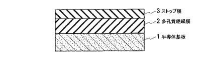
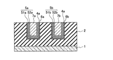
第1の実施の形態に係る半導体装置は、図1(a)に示すように、配線溝4a,4bを有し、比誘電率が3以下の多孔質絶縁膜2と、配線溝4a,4bの表面に沿って形成されたバリアメタル層5a,5bと、バリアメタル層5a,5bに接する多孔質絶縁膜2中に形成された金属浸透領域6a,6bと、バリアメタル層5a,5bを介して配線溝4a,4b中に埋め込まれた金属配線7a,7bとを備える。
(First embodiment)
As shown in FIG. 1A, the semiconductor device according to the first embodiment includes
多孔質絶縁膜2、配線溝4a,4b,バリアメタル層5a,5b,及び金属浸透領域6a,6bの下面には、半導体基板1が配置されている。多孔質絶縁膜2の上には、絶縁性の膜からなるストップ膜3が配置されている。バリアメタル層5a,5b及び金属配線7a,7bの一部は、ストップ膜3の中に形成されている。
The
図1(a)においては、第1の実施の形態に係る半導体装置の一例として、ダマシンプロセスにより製造可能な半導体装置を示している。図1(a)に示す半導体装置は、半導体基板1に形成されるトランジスタや素子分離領域、及び上層の配線等の説明を省略している。
FIG. 1A shows a semiconductor device that can be manufactured by a damascene process as an example of the semiconductor device according to the first embodiment. In the semiconductor device shown in FIG. 1A, description of transistors, element isolation regions, upper layer wirings, and the like formed on the
多孔質絶縁膜2としては、比誘電率が3以下のミクロな空孔を有する膜(porous-low-k膜)が好適である。多孔質絶縁膜2の材料は特に限定されないが、例えば、空孔率が10%以上、好ましくは10〜35%程度、比誘電率が1.5〜3.0程度、好ましくは2.0〜2.5程度の絶縁膜が好適である。
The porous
多孔質絶縁膜2の材料は、SiO2膜の密度を下げることにより比誘電率を3.9以下に制御した材料等が好適である。例えば、メチルシルセスオキサンポリマー(MSQ:CH3SiO1.5)、水シルセスオキサンポリマー(HSQ:H−SiO1.5)、ポーラスHSQ(H−SiOx)、ポーラスMSQ(CH3−SiO1.5)、又は有機シリカ(CH3−SiOx)が利用可能である。また、低い分極率を有する有機膜を用いた低誘電率絶縁膜も好適である。例えば、ポリテトラフルオロエチレン(PTFE)、ポリアリルエーテル(PAE)、ポーラスPAE、又はベンゾシクロブテン(BCB)等が利用可能である。
The material of the porous
多孔質絶縁膜2の配線溝4a,4bの表面に形成されたバリアメタル層5a,5bは、互いに膜密度の異なる2層以上の膜を有している。図1に示すバリアメタル層5a,5bは、配線溝4a,4b表面に形成された第1バリアメタル層51a,51b及び第1バリアメタル層51a,51b表面に形成された第2バリアメタル層52a,52bを有する。
The
第1バリアメタル層51a,51bは、表面に微細な凹凸を有する導電性の薄膜である。図1(b)は、図1(a)の点線部分の拡大図を示しているが、図1(b)に示すように、配線溝4aの側壁に接する第1バリアメタル層51aの膜厚tmは、1〜3nm程度である。配線溝4bの側壁に接する第1バリアメタル層51bの膜厚tnは、1〜3nm程度である。第1バリアメタル層51a,51bの材料としては、チタン(Ti)、ニオブ(Nb)、タンタル(Ta)、ルビジウム(Ru)、タングステン(W)、これら2種以上からなる合金、及びこれらの窒化物、酸化物、炭化物等の化合物が好適である。
The first
第2バリアメタル層52a,52bは、第1バリアメタル層51a,51bに比べて緻密質な膜である。第1バリアメタル層51aの側壁に接する第2バリアメタル層52aの膜厚tsは、1〜10nm程度である。第1バリアメタル層51bの側壁に接する第2バリアメタル層52aの膜厚ttは、1〜10nm程度である。第2バリアメタル層52a,52bの材料としては、Ti,Ta,Ru,W,Al、及びこれら2種以上からなる合金、これらの窒化物、酸化物、炭化物等の化合物が好適である。
The second
金属浸透領域6a,6bは、バリアメタル層5a,5bの成膜時のガスが多孔質絶縁膜2内に浸透することにより、多孔質絶縁膜2の細孔中に金属原子が固着した導電性領域である。金属浸透領域6aは、多孔質絶縁膜2と第1バリアメタル層51aとの間に配置されている。金属浸透領域6bは、多孔質絶縁膜2と第1バリアメタル層51bとの間に配置されている。
The
第1バリアメタル層51a、51bと多孔質絶縁膜2に接する金属浸透領域6a,6bの膜厚ta,tbは、金属配線7aと金属配線7bとの配線間最小距離(最小スペース)Lの1/20以下である。金属浸透領域6a,6bの膜厚ta,tbは、半導体装置の世代により異なるが、図1に半導体装置においては、膜厚ta,tbはそれぞれ1〜3.5nm程度である。
The film thicknesses t a and t b of the
金属配線7a,7bは、溝配線であっても、半導体基板1に形成されている(図示省略)不純物拡散層とのコンタクトプラグであってもよい。また、コンタクトプラグと溝配線とを一体化した構造であってもよい。金属配線7a,7bの材料としては、Al,Al−Cu合金、Cu等が利用可能である。
The
ストップ膜3は、複数の膜を含んでいてもよい。ストップ膜3の材料としては、炭化珪素(SiC)、窒化炭化珪素(SiCN)、窒化珪素(SiN)、炭化酸化珪素(SiOC),SiO2等の絶縁性の膜が利用可能である。
The
第1の実施の形態に係る半導体装置によれば、バリアメタル層5a,5bと多孔質絶縁膜2との間に金属浸透領域6a,6bが配置される。金属浸透領域6a,6bは、プロセス処理中の成膜ガス、水分等を多孔質絶縁膜2中へ過浸透させないための防壁として機能するため、金属、水分、ガス等の多孔質絶縁膜2中の拡散を抑制できる。この結果、配線のリーク等による配線容量の増大を抑制した半導体装置が提供できる。さらに、多孔質絶縁膜2とバリアメタル層5a,5bとの間に金属浸透領域6a,6bが存在することにより、多孔質絶縁膜2とバリアメタル層5a,5bとの密着性を向上させることができる。このため、多孔質絶縁膜2とバリアメタル層5a,5bとの間の剥離を防ぎ、歩留まりの高い半導体装置を提供することができる。
In the semiconductor device according to the first embodiment, the
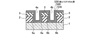
次に、図2〜図6を用いて、第1の実施の形態に係る半導体装置の製造方法を説明する。なお、以下に述べる半導体装置の製造方法は一例であり、この変形例を含めて、これ以外の種々の方法により実現可能であることは勿論である。 Next, a method for manufacturing the semiconductor device according to the first embodiment will be described with reference to FIGS. The semiconductor device manufacturing method described below is merely an example, and it is needless to say that the semiconductor device can be realized by various other methods including this modification.
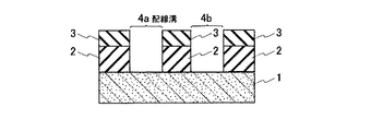
(a)図2に示すように、半導体基板1上に、CVD法等により、空孔率が10%以上、好ましくは10〜35%程度、比誘電率が1.5〜3.0程度、好ましくは2.0〜2.5程度の多孔質絶縁膜2を成膜する。この多孔質絶縁膜2の上に、CVD法等により、SiO2膜等のストップ膜3を成膜する。ストップ膜3の表面にフォトレジスト膜を塗布し、フォトリソグラフィ技術を用いてパターニングする。反応性イオンエッチング(RIE)法等により、パターニングされたフォトレジスト膜をマスクとして多孔質絶縁膜2及びストップ膜3の一部を選択的に除去し、図3に示すように、多孔質絶縁膜2及びストップ膜3を貫通する配線溝4a,4bを形成する。
(A) As shown in FIG. 2, the porosity is 10% or more on the
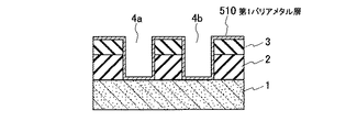
(b)図4に示すように、多孔質絶縁膜2、ストップ膜3、配線溝4a,4b上に、表面に凹凸を有する第1バリアメタル層510を成膜する。第1バリアメタル層510の成膜は、例えば、温度を300℃以下とし、Ti、Nb、Ta、Ru、W、これら2種以上からなる合金、及びこれらの窒化物、酸化物、炭化物等の化合物を用いて、スパッタ法により、配線溝4a,4bの側壁と接する部分の膜厚が1〜3nmとなるように制御しながら行う。
(B) As shown in FIG. 4, a first
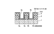
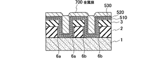
(c)引き続き、図5に示すように、第1バリアメタル層510の表面に、第1バリアメタル層510より膜密度の高い第2バリアメタル層520を形成する。第2バリアメタル層520の成膜は、例えば、温度を400℃以下とし、Ti,Ta,Ru,W,Al、これら2種以上からなる合金、及びこれらの窒化物、酸化物、炭化物等の化合物を用いて、CVD法或いはALD法等により、第1バリアメタル層510の側壁に接する部分の膜厚が1〜10nmとなるように制御しながら行う。この時、第2バリアメタル層52a,52bを成膜するための成膜ガスは、第1バリアメタル層510を介して多孔質絶縁膜2へ浸透する。この結果、成膜ガスに含まれる金属原子が多孔質絶縁膜2の細孔に固着され、導電性の金属浸透領域6a,6bが形成される。
(C) Subsequently, as shown in FIG. 5, a second
(d)図6に示すように、第2バリアメタル層520の表面に、電界めっき法等により金属膜700を堆積する。CMP法により、金属膜700をストップ膜3の表面が露出されるまで研磨すれば、図1(a)に示すような半導体装置が完成する。
(D) As shown in FIG. 6, a metal film 700 is deposited on the surface of the second
第1の実施の形態に係る半導体装置の製造方法によれば、CVD法又はALD法等により緻密な膜質の第2バリアメタル層52a,52bを成膜する前に、スパッタ法により第1バリアメタル層51a,51bを配線溝4a,4b表面に形成する。スパッタ法により形成された第1バリアメタル層51a,51bは、第2バリアメタル層52a,52bより膜密度が低く、表面に表面に微小な凹凸を有する。このため、第1バリアメタル層51a,51bと第2バリアメタル層52a、52bとの濡れ性を向上させ、剥離を防止することができる。
According to the method of manufacturing a semiconductor device according to the first embodiment, the first barrier metal is formed by sputtering before the dense second
また、膜密度の低い第1バリアメタル層51a,51bを形成した後に、CVD法又はALD法を用いて膜密度の高い第2バリアメタル層52a,52bを形成することにより、第2バリアメタル層52a,52bの成膜時のガスの多孔質絶縁膜2中への浸透量を調節できる。このため、外気や金属等の多孔質絶縁膜2中へ拡散を防止するための金属浸透領域6a,6bを、所望の膜厚に制御し、配線容量の増大を更に抑制することが可能となる。
In addition, after the first
なお、図2〜図6に例示する半導体装置の製造方法では、第1バリアメタル層51a、51bの膜厚tm,tnを1〜3nmに制御し、第2バリアメタル層52a,52bの膜厚ts,ttを1〜10nmに制御することで、金属浸透領域6a,6bの膜厚ta,tbを、金属配線7a,7bの配線間最小距離Lの1/20以下に制御している。
2 to 6, the film thicknesses t m and t n of the first
ここで、第1バリアメタル層51a,51bの膜厚tm,tnを1nm以上としたのは、スパッタ法により1nm堆積させた場合に、金属原子を10原子層程度に堆積させることができ、所望の量の成膜ガスを原子層の隙間から多孔質絶縁膜2に浸透させることができるからである。一方、第1バリアメタル層51a,51bの膜厚tm,tnを3nm以下としたのは、3nm以上堆積させることにより膜密度が高くなるとともに原子間の隙間が小さくなるため、多孔質絶縁膜2中に所望量の成膜ガスを浸透させにくくなるからである。
Here, the reason why the film thicknesses t m and t n of the first
また、金属浸透領域6a,6bの膜厚を、配線間最小距離Lの1/20以下となるように制御することにより、動作上、隣接する配線間のリークの問題や、多孔質絶縁膜2中への金属材料の拡散による配線容量増大の問題やリークの問題が顕在化しない程度に抑制できる。この結果、信頼性の高い半導体装置が製造できる。
Further, by controlling the film thickness of the
例えば、被誘電率が2.2で空孔率が30%の多孔質絶縁膜2に対し、配線間最小距離を70nmとして、配線溝4a,4bを形成する。引き続き、室温において、Tiを用いて配線溝4a,4bの側壁部分を1nm程度、底面部分を3nm程度となるように、スパッタ法により第1バリアメタル層51a,51bを形成する。その後、ALD法により、250℃でTaNを用いて膜厚1nm程度に第2バリアメタル層52a,52bを成膜する。この結果、金属浸透領域6a,6bの膜厚の合計を配線間最小距離(70nm)の10分の1以下である、6.9nm程度に制御することが可能となる。
For example, the
(第2の実施の形態)
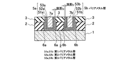
本発明の第2の実施の形態に係る半導体装置は、図7に示すように、バリアメタル層5a,5bのそれぞれが、第1バリアメタル層51a,51b,第2バリアメタル層52a,52b,及び第3バリアメタル層53a,53bの3層構造を備える点が、図1に示す半導体装置と異なる。
(Second Embodiment)
As shown in FIG. 7, in the semiconductor device according to the second embodiment of the present invention, each of the
第3バリアメタル層53a,53bは、第2バリアメタル層52a,52bの表面にそれぞれ配置された、第2バリアメタル層52a,52bより膜密度の低い導電性膜である。第3バリアメタル層53a,53bは、表面に微細な凹凸を有している。第2バリアメタル層52a,52bの側壁に接する第3バリアメタル層53a,53bの膜厚tu,tvは、それぞれ1〜3nm程度である。第3バリアメタル層53a,53bの材料としては、Ti、Nb、Ta、Ru、W、これら2種以上からなる合金、及びこれらの窒化物、酸化物、炭化物等の化合物が利用可能である。他は、第1の実施の形態に示す半導体装置と実質的に同様であるので、説明を省略する。
The third
図7に示す半導体装置によれば、表面が平坦で緻密質な膜質の第2バリアメタル層52a,52bの表面に、第2バリアメタル層52a,52bより膜密度の低い第3バリアメタル層53a,53bが配置される。第3バリアメタル層53a,53bは、表面に微細な凹凸を有するため、表面が平坦な第2バリアメタル層52a,52bに比べて、バリアメタル層5a,5bと金属配線7a,7bとの密着性を向上させることができる。この結果、バリアメタル層5a,5bと金属配線7a,7bとの間の剥離を防止でき、信頼性が更に向上する。
According to the semiconductor device shown in FIG. 7, the third
次に、図8及び図9を用いて、第2の実施の形態に係る半導体装置の製造方法を説明する。第1バリアメタル層51a,51bの表面に第2バリアメタル層52a,52bを成膜するまでの工程は、図2〜図5に示す工程と同様である。
Next, a method for manufacturing the semiconductor device according to the second embodiment will be described with reference to FIGS. The steps until the second
図8に示すように、第2バリアメタル層520の表面に、スパッタ法により第3バリアメタル層530を成膜する。第3バリアメタル層530の成膜は、例えば、温度を300℃以下とし、Ti、Nb、Ta、Ru、W及びこれら2種以上からなる合金、これらの窒化物、酸化物、炭化物等の化合物を用いて、スパッタ法により第2バリアメタル層52a,52b表面の側壁に接する部分の膜厚tu,tvが1〜3nm程度となるように制御しながら行う。
As shown in FIG. 8, a third
図9に示すように、第3バリアメタル層530の表面に、電界めっき法等により金属膜700を堆積する。CMP法により、金属膜700をストップ膜3の表面が露出されるまで研磨すれば、図7に示すような半導体装置が完成する。
As shown in FIG. 9, a metal film 700 is deposited on the surface of the third
第2の実施の形態に係る半導体装置の製造方法によれば、第2バリアメタル層52a,52bの表面に、表面に凹凸を有する第3バリアメタル層53a,53bを蒸着させることで、バリアメタル層5a,5bと金属配線7a,7bとの濡れ性を向上できる。この結果、バリアメタル層5a,5bと金属配線7a,7bとの剥離を防止でき、信頼性をより向上させることができる。
(その他の実施の形態)
上記のように、本発明は第1及び第2の実施の形態によって記載したが、この開示の一部をなす論述及び図面はこの発明を限定するものであると理解すべきではない。この開示から当業者には様々な代替実施の形態、実施例及び運用技術が明らかとなろう。
According to the method of manufacturing a semiconductor device according to the second embodiment, the third
(Other embodiments)
As described above, the present invention has been described according to the first and second embodiments. However, it should not be understood that the description and drawings constituting a part of this disclosure limit the present invention. From this disclosure, various alternative embodiments, examples and operational techniques will be apparent to those skilled in the art.
第1及び第2の実施の形態に係る半導体装置は、上述した構造に限られず、他にも様々な配線構造に採用可能である。例えば、図10に示すように、多孔質絶縁膜2の一部に配線溝4a、4bを形成し、配線溝4a,4bと多孔質絶縁膜2との間に沿って金属浸透領域6a,6bが形成されていても構わない。
The semiconductor devices according to the first and second embodiments are not limited to the structures described above, and can be applied to various other wiring structures. For example, as shown in FIG. 10,
また、図11に示すように、図1に示す半導体装置上に複数の絶縁膜を配置して、多層配線構造を構成することもできる。図11に示す半導体装置は、半導体基板1A上に配置された下層多孔質絶縁膜2A及び下層ストップ膜3Aに下層配線溝4A,4Bが形成され、この下層配線溝4A,4Bにそれぞれ下層バリアメタル層5A,5Bが堆積される。下層バリアメタル層5A,5Bは、第1下層バリアメタル層51A,51B及び第2下層バリアメタル層52A,52Bを有する。第1下層バリアメタル層51A,51Bと下層多孔質絶縁膜2Aとの接触面には、下層配線溝4A,4Bに接する部分に沿って膜厚が1〜3.5nmに制御された下層金属浸透領域6A,6Bが配置される。
In addition, as shown in FIG. 11, a multilayer wiring structure can be configured by arranging a plurality of insulating films on the semiconductor device shown in FIG. In the semiconductor device shown in FIG. 11,
下層ストップ膜3A上には、上層多孔質絶縁膜12A及び上層多孔質絶縁膜12上の上層ストップ膜13Aが形成される。上層多孔質絶縁膜12A及び上層ストップ膜13Aの中には、ダマシン法等により形成された上層金属配線17A,17B及び上層金属配線17A,17Bの周囲を取り巻く上層バリアメタル層15A,15Bが配置される。上層バリアメタル層15A,15Bは、第1上層バリアメタル層151A,151B及び第2上層バリアメタル層152A,152Bを有する。第1上層バリアメタル層151A,151Bと上層多孔質絶縁膜12Aとの接触面には、上層配線溝14A,14Bの側壁に接する部分の膜厚が1〜3.5nmに制御された上層金属浸透領域16A,16Bが配置される。
On the lower stop film 3A, an upper porous insulating film 12A and an upper stop film 13A on the upper porous insulating film 12 are formed. In the upper porous insulating film 12A and the upper stop film 13A, upper
また、上述した半導体装置の配線構造は、ロジックLSI、DRAM、SRAMに代表されるメモリLSIの他、ダイオード、IGBT、電界効果トランジスタ(FET)、静電誘導トランジスタ(SIT)、バイポーラトランジスタ(BJT)、静電誘導サイリスタ(SI)、GTOサイリスタ等の半導体素子上の多層配線構造に好適である。しかし、上述した半導体装置の構造及び製造方法は、半導体装置に限定されず,例えば液晶装置,磁気記録媒体,光記録媒体,薄膜磁気ヘッド,超伝導素子等の電子装置に利用可能であることは勿論である。例えば,薄膜磁気ヘッドの製造工程は,工程数は少ないものの,半導体集積回路と同様なCVD工程,フォトリソグラフィ工程,エッチング工程等の繰り返しからなるものであり,本発明の構造及び製造方法が適用できることは容易に理解できるであろう。 The wiring structure of the semiconductor device described above includes a memory LSI represented by a logic LSI, DRAM, and SRAM, as well as a diode, IGBT, a field effect transistor (FET), a static induction transistor (SIT), and a bipolar transistor (BJT). It is suitable for multilayer wiring structures on semiconductor elements such as electrostatic induction thyristors (SI) and GTO thyristors. However, the structure and manufacturing method of the semiconductor device described above are not limited to the semiconductor device, and can be used for electronic devices such as liquid crystal devices, magnetic recording media, optical recording media, thin film magnetic heads, superconducting elements, and the like. Of course. For example, the manufacturing process of a thin film magnetic head is composed of repetition of the CVD process, the photolithography process, the etching process and the like similar to the semiconductor integrated circuit, although the number of processes is small, and the structure and the manufacturing method of the present invention can be applied. Will be easily understood.
このように、本発明はここでは記載していない様々な実施の形態等を含むことは勿論である。したがって、本発明の技術的範囲は上記の説明から妥当な特許請求の範囲に係る発明特定事項によってのみ定められるものである。 As described above, the present invention naturally includes various embodiments not described herein. Therefore, the technical scope of the present invention is defined only by the invention specifying matters according to the scope of claims reasonable from the above description.
1…半導体基板
2…多孔質絶縁膜
3…ストップ膜
4a,4b…配線溝
5a,5b…バリアメタル層
6a,6b…金属浸透領域
7a,7b…金属配線
51a,51b…第1バリアメタル層
52a,52b…第2バリアメタル層
53a,53b…第3バリアメタル層
DESCRIPTION OF
Claims (5)
前記半導体基板上に配置され、配線溝を有し、比誘電率が3以下の多孔質絶縁膜と、
前記配線溝の表面に沿って形成され、互いに膜密度の異なる複数の膜を有するバリアメタル層と、
前記バリアメタル層と接する前記多孔質絶縁膜中に形成された金属浸透領域と、
前記バリアメタル層を介して前記配線溝中に埋め込まれた金属配線
とを備えることを特徴とする半導体装置。 A semiconductor substrate;
A porous insulating film disposed on the semiconductor substrate, having a wiring groove, and having a relative dielectric constant of 3 or less;
A barrier metal layer formed along the surface of the wiring trench and having a plurality of films having different film densities;
A metal permeation region formed in the porous insulating film in contact with the barrier metal layer;
And a metal wiring embedded in the wiring groove through the barrier metal layer.
前記配線溝の表面に形成された第1バリアメタル層と、
前記第1バリアメタル層の表面に形成された前記第1バリアメタル層より緻密質の第2バリアメタル層
とを含むことを特徴とする請求項1に記載の半導体装置。 The barrier metal layer is
A first barrier metal layer formed on a surface of the wiring groove;
2. The semiconductor device according to claim 1, further comprising a second barrier metal layer denser than the first barrier metal layer formed on a surface of the first barrier metal layer.
前記多孔質絶縁膜中に配線溝を形成するステップと、
前記配線溝の表面に、互いに膜密度の異なる複数の膜を有するバリアメタル層を形成するステップと、
前記バリアメタル層と接する前記多孔質絶縁膜中に金属浸透領域を形成するステップと、
前記バリアメタル層を介して前記配線溝の中に金属配線を形成するステップ
とを備えることを特徴とする半導体装置の製造方法。 Forming a porous insulating film having a relative dielectric constant of 3 or less on a semiconductor substrate;
Forming a wiring groove in the porous insulating film;
Forming a barrier metal layer having a plurality of films having different film densities on the surface of the wiring trench;
Forming a metal permeation region in the porous insulating film in contact with the barrier metal layer;
Forming a metal wiring in the wiring groove through the barrier metal layer. A method for manufacturing a semiconductor device, comprising:
5. The semiconductor according to claim 4, wherein the first barrier metal layer is formed by sputtering, and the second barrier metal layer is formed by one of a chemical vapor deposition method and an atomic layer deposition method. Device manufacturing method.
Priority Applications (2)
| Application Number | Priority Date | Filing Date | Title |
|---|---|---|---|
| JP2005002637A JP2006190884A (en) | 2005-01-07 | 2005-01-07 | Semiconductor device and manufacturing method of semiconductor device |
| US11/218,722 US20060154464A1 (en) | 2005-01-07 | 2005-09-06 | Semiconductor device and a method of fabricating a semiconductor device |
Applications Claiming Priority (1)
| Application Number | Priority Date | Filing Date | Title |
|---|---|---|---|
| JP2005002637A JP2006190884A (en) | 2005-01-07 | 2005-01-07 | Semiconductor device and manufacturing method of semiconductor device |
Publications (1)
| Publication Number | Publication Date |
|---|---|
| JP2006190884A true JP2006190884A (en) | 2006-07-20 |
Family
ID=36653821
Family Applications (1)
| Application Number | Title | Priority Date | Filing Date |
|---|---|---|---|
| JP2005002637A Abandoned JP2006190884A (en) | 2005-01-07 | 2005-01-07 | Semiconductor device and manufacturing method of semiconductor device |
Country Status (2)
| Country | Link |
|---|---|
| US (1) | US20060154464A1 (en) |
| JP (1) | JP2006190884A (en) |
Cited By (3)
| Publication number | Priority date | Publication date | Assignee | Title |
|---|---|---|---|---|
| JP2010177305A (en) * | 2009-01-28 | 2010-08-12 | Fujitsu Semiconductor Ltd | Semiconductor device and manufacturing method thereof |
| US9006900B2 (en) | 2013-03-11 | 2015-04-14 | Taiwan Semiconductor Manufacturing Co., Ltd. | Semiconductor device with advanced pad structure resistant to plasma damage and method for forming the same |
| KR20160124001A (en) | 2015-04-16 | 2016-10-26 | 르네사스 일렉트로닉스 가부시키가이샤 | Semiconductor device and method of manufacturing same |
Families Citing this family (9)
| Publication number | Priority date | Publication date | Assignee | Title |
|---|---|---|---|---|
| US20070126120A1 (en) * | 2005-12-06 | 2007-06-07 | Taiwan Semiconductor Manufacturing Co., Ltd. | Semiconductor device |
| US7417321B2 (en) * | 2005-12-30 | 2008-08-26 | Taiwan Semiconductor Manufacturing Co., Ltd | Via structure and process for forming the same |
| US20070189067A1 (en) * | 2006-02-15 | 2007-08-16 | Francis Goodwin | Dynamic memory |
| US20070278682A1 (en) * | 2006-05-31 | 2007-12-06 | Chung-Chi Ko | Self-assembled mono-layer liner for cu/porous low-k interconnections |
| JP5194393B2 (en) * | 2006-06-23 | 2013-05-08 | 東京エレクトロン株式会社 | Manufacturing method of semiconductor device |
| KR100782487B1 (en) * | 2006-08-21 | 2007-12-05 | 삼성전자주식회사 | Void confinement structures, semiconductor devices having the void confinement structures and methods of forming them |
| US7466027B2 (en) * | 2006-09-13 | 2008-12-16 | Taiwan Semiconductor Manufacturing Co., Ltd. | Interconnect structures with surfaces roughness improving liner and methods for fabricating the same |
| KR100808601B1 (en) * | 2006-12-28 | 2008-02-29 | 주식회사 하이닉스반도체 | Multi-layer metallization method of semiconductor device using damascene process |
| US7704884B2 (en) * | 2008-04-11 | 2010-04-27 | Micron Technology, Inc. | Semiconductor processing methods |
Family Cites Families (8)
| Publication number | Priority date | Publication date | Assignee | Title |
|---|---|---|---|---|
| US6482733B2 (en) * | 2000-05-15 | 2002-11-19 | Asm Microchemistry Oy | Protective layers prior to alternating layer deposition |
| US6586334B2 (en) * | 2000-11-09 | 2003-07-01 | Texas Instruments Incorporated | Reducing copper line resistivity by smoothing trench and via sidewalls |
| US6537896B1 (en) * | 2001-12-04 | 2003-03-25 | Lsi Logic Corporation | Process for treating porous low k dielectric material in damascene structure to form a non-porous dielectric diffusion barrier on etched via and trench surfaces in the porous low k dielectric material |
| US6528409B1 (en) * | 2002-04-29 | 2003-03-04 | Advanced Micro Devices, Inc. | Interconnect structure formed in porous dielectric material with minimized degradation and electromigration |
| KR100465058B1 (en) * | 2002-12-26 | 2005-01-05 | 매그나칩 반도체 유한회사 | Method of forming a barrier metal in a semiconductor device |
| US6952052B1 (en) * | 2004-03-30 | 2005-10-04 | Advanced Micro Devices, Inc. | Cu interconnects with composite barrier layers for wafer-to-wafer uniformity |
| KR100590386B1 (en) * | 2004-04-20 | 2006-06-19 | 매그나칩 반도체 유한회사 | Metal wiring formation method of semiconductor device |
| US7015150B2 (en) * | 2004-05-26 | 2006-03-21 | International Business Machines Corporation | Exposed pore sealing post patterning |
-
2005
- 2005-01-07 JP JP2005002637A patent/JP2006190884A/en not_active Abandoned
- 2005-09-06 US US11/218,722 patent/US20060154464A1/en not_active Abandoned
Cited By (7)
| Publication number | Priority date | Publication date | Assignee | Title |
|---|---|---|---|---|
| JP2010177305A (en) * | 2009-01-28 | 2010-08-12 | Fujitsu Semiconductor Ltd | Semiconductor device and manufacturing method thereof |
| US9006900B2 (en) | 2013-03-11 | 2015-04-14 | Taiwan Semiconductor Manufacturing Co., Ltd. | Semiconductor device with advanced pad structure resistant to plasma damage and method for forming the same |
| KR101524920B1 (en) * | 2013-03-11 | 2015-06-01 | 타이완 세미콘덕터 매뉴팩쳐링 컴퍼니 리미티드 | Semiconductor device with advanced pad structure resistant to plasma damage and method for forming the same |
| US9385081B2 (en) | 2013-03-11 | 2016-07-05 | Taiwan Semiconductor Manufacturing Co., Ltd. | Semiconductor device with advanced pad structure resistant to plasma damage and method for forming the same |
| US9666545B2 (en) | 2013-03-11 | 2017-05-30 | Taiwan Semiconductor Manufacturing Co., Ltd. | Semiconductor device with advanced pad structure resistant to plasma damage and metnod for forming same |
| KR20160124001A (en) | 2015-04-16 | 2016-10-26 | 르네사스 일렉트로닉스 가부시키가이샤 | Semiconductor device and method of manufacturing same |
| JP2016207722A (en) * | 2015-04-16 | 2016-12-08 | ルネサスエレクトロニクス株式会社 | Semiconductor device and manufacturing method thereof |
Also Published As
| Publication number | Publication date |
|---|---|
| US20060154464A1 (en) | 2006-07-13 |
Similar Documents
| Publication | Publication Date | Title |
|---|---|---|
| US8178437B2 (en) | Barrier material and process for Cu interconnect | |
| JP3778487B2 (en) | Method for forming metal capacitor | |
| US7052990B2 (en) | Sealed pores in low-k material damascene conductive structures | |
| KR101456780B1 (en) | Capping layer for improved deposition selectivity | |
| JP3031301B2 (en) | Copper wiring structure and method of manufacturing the same | |
| KR20050106504A (en) | Method for manufacturing a semiconductor component having a barrier-lined opening | |
| JP5385610B2 (en) | Method for forming an interconnect structure | |
| JP2006190884A (en) | Semiconductor device and manufacturing method of semiconductor device | |
| US20080054454A1 (en) | Semiconductor device and method for manufacturing semiconductor device | |
| EP1610376A1 (en) | Semiconductor device | |
| JPWO2006046487A1 (en) | Semiconductor device and manufacturing method of semiconductor device | |
| US20060261483A1 (en) | Semiconductor device and method for manufacturing the same | |
| JP2005005383A (en) | Semiconductor device and manufacturing method of semiconductor device | |
| JP2008147562A (en) | Semiconductor device manufacturing method and semiconductor device | |
| US10825720B2 (en) | Single trench damascene interconnect using TiN HMO | |
| JP2005203568A (en) | Fabrication process of semiconductor device, and semiconductor device | |
| US12400875B2 (en) | Film deposition for patterning process | |
| JP2005129937A (en) | Low K integrated circuit interconnection structure | |
| JP4447433B2 (en) | Semiconductor device manufacturing method and semiconductor device | |
| US7026225B1 (en) | Semiconductor component and method for precluding stress-induced void formation in the semiconductor component | |
| US12438039B2 (en) | Air gap in beol interconnect | |
| CN100481383C (en) | Method for manufacturing semiconductor device and semiconductor device | |
| US20240153864A1 (en) | Metallization levels with skip via and dielectric layer | |
| JP2011109036A (en) | Semiconductor device, and method for manufacturing the same | |
| KR100483838B1 (en) | Dual damascene process of metal wire |
Legal Events
| Date | Code | Title | Description |
|---|---|---|---|
| A621 | Written request for application examination |
Free format text: JAPANESE INTERMEDIATE CODE: A621 Effective date: 20071012 |
|
| A762 | Written abandonment of application |
Free format text: JAPANESE INTERMEDIATE CODE: A762 Effective date: 20080307 |