JP2006145992A - Liquid crystal display and its manufacturing method - Google Patents
Liquid crystal display and its manufacturing method Download PDFInfo
- Publication number
- JP2006145992A JP2006145992A JP2004337916A JP2004337916A JP2006145992A JP 2006145992 A JP2006145992 A JP 2006145992A JP 2004337916 A JP2004337916 A JP 2004337916A JP 2004337916 A JP2004337916 A JP 2004337916A JP 2006145992 A JP2006145992 A JP 2006145992A
- Authority
- JP
- Japan
- Prior art keywords
- liquid crystal
- crystal display
- display device
- photoinitiator
- substrates
- Prior art date
- Legal status (The legal status is an assumption and is not a legal conclusion. Google has not performed a legal analysis and makes no representation as to the accuracy of the status listed.)
- Pending
Links
Images


Classifications
-
- C—CHEMISTRY; METALLURGY
- C09—DYES; PAINTS; POLISHES; NATURAL RESINS; ADHESIVES; COMPOSITIONS NOT OTHERWISE PROVIDED FOR; APPLICATIONS OF MATERIALS NOT OTHERWISE PROVIDED FOR
- C09K—MATERIALS FOR MISCELLANEOUS APPLICATIONS, NOT PROVIDED FOR ELSEWHERE
- C09K19/00—Liquid crystal materials
- C09K19/52—Liquid crystal materials characterised by components which are not liquid crystals, e.g. additives with special physical aspect: solvents, solid particles
- C09K19/54—Additives having no specific mesophase characterised by their chemical composition
- C09K19/56—Aligning agents
-
- G—PHYSICS
- G02—OPTICS
- G02F—OPTICAL DEVICES OR ARRANGEMENTS FOR THE CONTROL OF LIGHT BY MODIFICATION OF THE OPTICAL PROPERTIES OF THE MEDIA OF THE ELEMENTS INVOLVED THEREIN; NON-LINEAR OPTICS; FREQUENCY-CHANGING OF LIGHT; OPTICAL LOGIC ELEMENTS; OPTICAL ANALOGUE/DIGITAL CONVERTERS
- G02F1/00—Devices or arrangements for the control of the intensity, colour, phase, polarisation or direction of light arriving from an independent light source, e.g. switching, gating or modulating; Non-linear optics
- G02F1/01—Devices or arrangements for the control of the intensity, colour, phase, polarisation or direction of light arriving from an independent light source, e.g. switching, gating or modulating; Non-linear optics for the control of the intensity, phase, polarisation or colour
- G02F1/13—Devices or arrangements for the control of the intensity, colour, phase, polarisation or direction of light arriving from an independent light source, e.g. switching, gating or modulating; Non-linear optics for the control of the intensity, phase, polarisation or colour based on liquid crystals, e.g. single liquid crystal display cells
- G02F1/133—Constructional arrangements; Operation of liquid crystal cells; Circuit arrangements
- G02F1/1333—Constructional arrangements; Manufacturing methods
- G02F1/1337—Surface-induced orientation of the liquid crystal molecules, e.g. by alignment layers
- G02F1/133707—Structures for producing distorted electric fields, e.g. bumps, protrusions, recesses, slits in pixel electrodes
-
- G—PHYSICS
- G02—OPTICS
- G02F—OPTICAL DEVICES OR ARRANGEMENTS FOR THE CONTROL OF LIGHT BY MODIFICATION OF THE OPTICAL PROPERTIES OF THE MEDIA OF THE ELEMENTS INVOLVED THEREIN; NON-LINEAR OPTICS; FREQUENCY-CHANGING OF LIGHT; OPTICAL LOGIC ELEMENTS; OPTICAL ANALOGUE/DIGITAL CONVERTERS
- G02F1/00—Devices or arrangements for the control of the intensity, colour, phase, polarisation or direction of light arriving from an independent light source, e.g. switching, gating or modulating; Non-linear optics
- G02F1/01—Devices or arrangements for the control of the intensity, colour, phase, polarisation or direction of light arriving from an independent light source, e.g. switching, gating or modulating; Non-linear optics for the control of the intensity, phase, polarisation or colour
- G02F1/13—Devices or arrangements for the control of the intensity, colour, phase, polarisation or direction of light arriving from an independent light source, e.g. switching, gating or modulating; Non-linear optics for the control of the intensity, phase, polarisation or colour based on liquid crystals, e.g. single liquid crystal display cells
- G02F1/133—Constructional arrangements; Operation of liquid crystal cells; Circuit arrangements
- G02F1/1333—Constructional arrangements; Manufacturing methods
- G02F1/1337—Surface-induced orientation of the liquid crystal molecules, e.g. by alignment layers
- G02F1/133753—Surface-induced orientation of the liquid crystal molecules, e.g. by alignment layers with different alignment orientations or pretilt angles on a same surface, e.g. for grey scale or improved viewing angle
-
- G—PHYSICS
- G02—OPTICS
- G02F—OPTICAL DEVICES OR ARRANGEMENTS FOR THE CONTROL OF LIGHT BY MODIFICATION OF THE OPTICAL PROPERTIES OF THE MEDIA OF THE ELEMENTS INVOLVED THEREIN; NON-LINEAR OPTICS; FREQUENCY-CHANGING OF LIGHT; OPTICAL LOGIC ELEMENTS; OPTICAL ANALOGUE/DIGITAL CONVERTERS
- G02F1/00—Devices or arrangements for the control of the intensity, colour, phase, polarisation or direction of light arriving from an independent light source, e.g. switching, gating or modulating; Non-linear optics
- G02F1/01—Devices or arrangements for the control of the intensity, colour, phase, polarisation or direction of light arriving from an independent light source, e.g. switching, gating or modulating; Non-linear optics for the control of the intensity, phase, polarisation or colour
- G02F1/13—Devices or arrangements for the control of the intensity, colour, phase, polarisation or direction of light arriving from an independent light source, e.g. switching, gating or modulating; Non-linear optics for the control of the intensity, phase, polarisation or colour based on liquid crystals, e.g. single liquid crystal display cells
- G02F1/137—Devices or arrangements for the control of the intensity, colour, phase, polarisation or direction of light arriving from an independent light source, e.g. switching, gating or modulating; Non-linear optics for the control of the intensity, phase, polarisation or colour based on liquid crystals, e.g. single liquid crystal display cells characterised by the electro-optical or magneto-optical effect, e.g. field-induced phase transition, orientation effect, guest-host interaction or dynamic scattering
- G02F1/139—Devices or arrangements for the control of the intensity, colour, phase, polarisation or direction of light arriving from an independent light source, e.g. switching, gating or modulating; Non-linear optics for the control of the intensity, phase, polarisation or colour based on liquid crystals, e.g. single liquid crystal display cells characterised by the electro-optical or magneto-optical effect, e.g. field-induced phase transition, orientation effect, guest-host interaction or dynamic scattering based on orientation effects in which the liquid crystal remains transparent
- G02F1/1393—Devices or arrangements for the control of the intensity, colour, phase, polarisation or direction of light arriving from an independent light source, e.g. switching, gating or modulating; Non-linear optics for the control of the intensity, phase, polarisation or colour based on liquid crystals, e.g. single liquid crystal display cells characterised by the electro-optical or magneto-optical effect, e.g. field-induced phase transition, orientation effect, guest-host interaction or dynamic scattering based on orientation effects in which the liquid crystal remains transparent the birefringence of the liquid crystal being electrically controlled, e.g. ECB-, DAP-, HAN-, PI-LC cells
-
- G—PHYSICS
- G02—OPTICS
- G02F—OPTICAL DEVICES OR ARRANGEMENTS FOR THE CONTROL OF LIGHT BY MODIFICATION OF THE OPTICAL PROPERTIES OF THE MEDIA OF THE ELEMENTS INVOLVED THEREIN; NON-LINEAR OPTICS; FREQUENCY-CHANGING OF LIGHT; OPTICAL LOGIC ELEMENTS; OPTICAL ANALOGUE/DIGITAL CONVERTERS
- G02F1/00—Devices or arrangements for the control of the intensity, colour, phase, polarisation or direction of light arriving from an independent light source, e.g. switching, gating or modulating; Non-linear optics
- G02F1/01—Devices or arrangements for the control of the intensity, colour, phase, polarisation or direction of light arriving from an independent light source, e.g. switching, gating or modulating; Non-linear optics for the control of the intensity, phase, polarisation or colour
- G02F1/13—Devices or arrangements for the control of the intensity, colour, phase, polarisation or direction of light arriving from an independent light source, e.g. switching, gating or modulating; Non-linear optics for the control of the intensity, phase, polarisation or colour based on liquid crystals, e.g. single liquid crystal display cells
- G02F1/133—Constructional arrangements; Operation of liquid crystal cells; Circuit arrangements
- G02F1/1333—Constructional arrangements; Manufacturing methods
- G02F1/1337—Surface-induced orientation of the liquid crystal molecules, e.g. by alignment layers
- G02F1/133776—Surface-induced orientation of the liquid crystal molecules, e.g. by alignment layers having structures locally influencing the alignment, e.g. unevenness
Landscapes
- Physics & Mathematics (AREA)
- Nonlinear Science (AREA)
- Chemical & Material Sciences (AREA)
- Crystallography & Structural Chemistry (AREA)
- General Physics & Mathematics (AREA)
- Optics & Photonics (AREA)
- Mathematical Physics (AREA)
- Spectroscopy & Molecular Physics (AREA)
- Engineering & Computer Science (AREA)
- Materials Engineering (AREA)
- Organic Chemistry (AREA)
- Liquid Crystal (AREA)
- Polymerisation Methods In General (AREA)
Abstract
Description
本発明は、液晶表示装置及びその製造方法に関し、特に、液晶分子が電圧無印加時に基板面にほぼ垂直に配向する垂直配向型の液晶表示装置及びその製造方法に関する。 The present invention relates to a liquid crystal display device and a manufacturing method thereof, and more particularly to a vertical alignment type liquid crystal display device in which liquid crystal molecules are aligned substantially perpendicular to a substrate surface when no voltage is applied, and a manufacturing method thereof.
従来、アクティブマトリクス型の液晶表示装置(LCD)としては、正の誘電率異方性を持つ液晶材料を基板面に水平に、かつ対向する基板間で90度ツイストするように配向させたTN(Twisted Nematic)モードの液晶表示装置が広く用いられている。しかし、TNモードの液晶表示装置は視角特性が悪いという問題を有しているため、視角特性を改善すべく種々の検討が行われている。 Conventionally, as an active matrix type liquid crystal display device (LCD), a liquid crystal material having a positive dielectric anisotropy is aligned TN (horizontal to the substrate surface) and twisted by 90 degrees between opposing substrates. A liquid crystal display device in a Twisted Nematic mode is widely used. However, since the TN mode liquid crystal display device has a problem of poor viewing angle characteristics, various studies have been made to improve the viewing angle characteristics.
TNモードに替わる方式として、負の誘電率異方性を持つ液晶材料を垂直配向させ、かつ基板表面に設けた突起やスリットにより電圧印加時の液晶分子の傾斜方向を規制するMVA(Multi−domain Vertical Alignment)方式の液晶表示装置が開発されている。MVA方式の液晶表示装置では、視角特性の大幅な改善に成功している。 As an alternative to the TN mode, an MVA (Multi-domain) that vertically aligns a liquid crystal material having negative dielectric anisotropy and regulates the tilt direction of liquid crystal molecules when a voltage is applied by projections and slits provided on the substrate surface. A vertical alignment type liquid crystal display device has been developed. The MVA liquid crystal display device has succeeded in greatly improving the viewing angle characteristics.
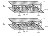
一般的なMVA方式の液晶表示装置について図9及び図10を用いて説明する。図9は、MVA方式の液晶表示装置の断面を斜めから見た概念図である。図10は、MVA方式の液晶表示装置の3画素分の構成及び液晶分子の配向方向を示す概念図である。図9(a)、(b)に示すように、MVA方式の液晶表示装置では、負の誘電率異方性を有する液晶材料の液晶分子108が、2枚のガラス基板110、111の間で基板面にほぼ垂直に配向している。図示していないが、一方のガラス基板110上には薄膜トランジスタ(TFT)に接続された画素電極が画素領域毎に形成されており、他方のガラス基板111上の全面には共通電極が形成されている。画素電極上には突起120が形成され、共通電極上には突起121が形成されている。突起120、121は交互に配列するように配置されている。画素電極、共通電極及び突起120、121上には、不図示の垂直配向膜が塗布形成されている。
A general MVA liquid crystal display device will be described with reference to FIGS. FIG. 9 is a conceptual view of a cross section of an MVA liquid crystal display device as viewed from an oblique direction. FIG. 10 is a conceptual diagram showing the configuration of three pixels of the MVA liquid crystal display device and the alignment direction of liquid crystal molecules. As shown in FIGS. 9A and 9B, in the MVA liquid crystal display device, the
TFTがオフ状態で液晶分子108に電圧が印加されていない場合には、図9(a)に示すように、液晶分子108は基板界面にほぼ垂直に配向している。そして、TFTをオン状態にした場合には、液晶分子108に所定の電圧が印加され、突起120、121の形成構造によって液晶分子108の傾斜方向が規制される。これにより液晶分子108は、図9(b)に示すように複数の方向に配向する。例えば、図10のように突起120、121が形成されている場合には、液晶分子108は一画素内でA、B、C及びDの4方向にそれぞれ配向する。このようにMVA方式の液晶表示装置では、TFTをオン状態にした際に液晶分子108が一画素内で複数の方向に配向するので、良好な視角特性が得られる。
When the TFT is off and no voltage is applied to the
MVA方式の液晶表示装置では、液晶分子108の傾斜方向は配向膜により規制されている訳ではない。したがってMVA方式は、TNモードを代表とする水平配向方式では必須であるラビング等の配向処理工程を必要としない。これにより、ラビングにより生じる静電気やゴミの問題をなくし、配向処理後の洗浄工程も不要であるというプロセス上の利点がある。また、プレティルトのばらつきによる表示むらが生じないという表示品質上の利点もある。上記のようにMVA方式の液晶表示装置は、製造プロセスの簡略化及び製造歩留りの向上により低コスト化が可能であり、また高い表示品質が得られるという特徴を有している。
In the MVA liquid crystal display device, the tilt direction of the
しかしながら、ラビングが不要なMVA方式の液晶表示装置といえども配向膜の塗布形成は必要である。このため、配向膜印刷工程で生じる膜厚むらや異物の混入などによって製造歩留りが低下し、部材費やタクトタイムが増加してしまう。このように、従来のMVA方式の液晶表示装置には、配向膜印刷工程に起因して製造コストが増加してしまうという問題が依然として存在する。 However, even with an MVA liquid crystal display device that does not require rubbing, it is necessary to apply and form an alignment film. For this reason, the manufacturing yield decreases due to film thickness unevenness or foreign matter mixed in the alignment film printing process, and the member cost and tact time increase. As described above, the conventional MVA liquid crystal display device still has a problem that the manufacturing cost increases due to the alignment film printing process.
また、近年は液晶表示装置の大型化等に対応してマザーガラスの超大型化が進んでいる。ところが配向膜印刷装置は、超大型化が進むマザーガラスに対応していくことが困難である。さらに近年は、薄型で柔軟なフィルム状の基板や、平面ではなく屈曲した形状の基板なども用いられるようになっている。これらの基板に配向膜を印刷するのは極めて困難である。このため、大型のマザーガラスや特殊な形状の基板を用いた液晶表示装置は、良好な液晶配向を得るのが困難であるという問題を有している。 In recent years, the mother glass has been increased in size in response to an increase in the size of liquid crystal display devices. However, it is difficult for the alignment film printing apparatus to cope with the mother glass whose size is increasing. Further, in recent years, a thin and flexible film-like substrate, a bent substrate instead of a flat surface, and the like have been used. It is extremely difficult to print alignment films on these substrates. For this reason, a liquid crystal display device using a large mother glass or a specially shaped substrate has a problem that it is difficult to obtain good liquid crystal alignment.
本発明の目的は、製造コストをさらに低減できる液晶表示装置及びその製造方法を提供することにある。 An object of the present invention is to provide a liquid crystal display device and a manufacturing method thereof that can further reduce manufacturing costs.
また本発明の目的は、大型のマザーガラスや特殊な形状の基板を用いても良好な液晶配向の得られる液晶表示装置及びその製造方法を提供することにある。 Another object of the present invention is to provide a liquid crystal display device and a method for manufacturing the liquid crystal display device which can obtain good liquid crystal alignment even when a large mother glass or a specially shaped substrate is used.
上記目的は、対向配置された一対の基板と、前記一対の基板間に封止された液晶と、前記液晶に混入された重合性成分が、塩素原子を含まない光開始剤により反応が促進されて重合し、前記一対の基板との界面近傍に形成され、前記液晶を配向制御する光硬化物とを有することを特徴とする液晶表示装置によって達成される。 The above-described object is that the reaction between a pair of substrates opposed to each other, a liquid crystal sealed between the pair of substrates, and a polymerizable component mixed in the liquid crystal is accelerated by a photoinitiator that does not contain a chlorine atom. And a photocured material that is formed in the vicinity of the interface between the pair of substrates and that controls the alignment of the liquid crystal.
本発明によれば、製造コストをさらに低減できる液晶表示装置を実現できる。また、本発明によれば、大型のマザーガラスや特殊な形状の基板を用いても良好な液晶配向の得られる液晶表示装置を実現できる。 According to the present invention, a liquid crystal display device that can further reduce the manufacturing cost can be realized. Further, according to the present invention, it is possible to realize a liquid crystal display device capable of obtaining good liquid crystal alignment even when a large mother glass or a specially shaped substrate is used.
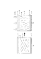
本発明の一実施の形態による液晶表示装置及びその製造方法について図1乃至図8を用いて説明する。図1は、本実施の形態による液晶表示装置の概略構成及びその製造方法を示している。まず、図1(a)に示すように、重合性成分と塩素原子を含まない光開始剤とが混入され、負の誘電率異方性を有する液晶6を一対の基板2、4間に封止する。本実施の形態では基板2、4上に垂直配向膜を塗布形成していないため、この段階の液晶分子8は基板面にほぼ平行に配向する。次に、図1(b)に示すように、紫外線(又は可視光)を液晶6に照射し、光開始剤により反応を促進させて重合性成分を重合させる。これにより、紫外線硬化物(光硬化物)30が、基板2、4との界面近傍に形成される。紫外線硬化物30は液晶6を配向規制する機能を有し、液晶分子8は基板面にほぼ垂直に配向する。
A liquid crystal display device and a manufacturing method thereof according to an embodiment of the present invention will be described with reference to FIGS. FIG. 1 shows a schematic configuration of a liquid crystal display device according to the present embodiment and a manufacturing method thereof. First, as shown in FIG. 1A, a liquid crystal 6 having a negative dielectric anisotropy mixed with a polymerizable component and a photoinitiator containing no chlorine atom is sealed between a pair of
本願出願人による日本国特許出願(特願2003−85220号、及び特願2003−420578号)では、配向膜を塗布形成せずに良好な液晶配向を得るための紫外線硬化物の構造及び形成方法が提案されている。これらの特許出願には、配向膜を塗布形成した液晶表示装置と同レベルの初期特性が得られる液晶表示装置が記載されている。しかしながら、鋭意試行の結果、液晶の良好な垂直配向性と長期的な信頼性とを両立させるためには、紫外線硬化物の形成条件のより一層の最適化が必要であることが分かった。 In the Japanese patent applications (Japanese Patent Application Nos. 2003-85220 and 2003-420578) filed by the applicant of the present application, the structure and forming method of an ultraviolet cured product for obtaining good liquid crystal alignment without coating and forming an alignment film. Has been proposed. These patent applications describe a liquid crystal display device that can obtain the same initial characteristics as a liquid crystal display device formed by applying an alignment film. However, as a result of diligent trials, it has been found that in order to achieve both good vertical alignment of liquid crystals and long-term reliability, it is necessary to further optimize the formation conditions of the ultraviolet cured product.
液晶の劣化による電圧保持率の低下を考慮すると、液晶に照射できる紫外線の照射強度および照射量には上限がある。このため、光開始剤を液晶に添加していない場合、紫外線照射後の液晶中のモノマー残存率は一般に40%以上であり、かなり高くなっている。このように高い残存率でモノマーが残存していても、配向膜が塗布形成された従来の液晶表示装置と同レベルの初期特性(電圧保持率、残留DC値等)を得ることは可能である。しかし、長期放置試験での特性劣化が大きいこと、及びMVA方式の液晶表示装置に適用した場合にはコモン電圧が時間により変動すること等の問題が生じるため、配向膜が塗布形成された従来の液晶表示装置と真に同レベルの特性が得られるとは言えない。 Considering a decrease in voltage holding ratio due to deterioration of the liquid crystal, there is an upper limit to the irradiation intensity and irradiation amount of ultraviolet rays that can be irradiated to the liquid crystal. For this reason, when the photoinitiator is not added to the liquid crystal, the residual ratio of the monomer in the liquid crystal after ultraviolet irradiation is generally 40% or more, which is considerably high. Even if the monomer remains in such a high residual ratio, it is possible to obtain initial characteristics (voltage holding ratio, residual DC value, etc.) of the same level as those of a conventional liquid crystal display device coated with an alignment film. . However, problems such as large deterioration of characteristics in the long-term standing test and fluctuation of the common voltage with time when applied to an MVA type liquid crystal display device occur. It cannot be said that the same level of characteristics as a liquid crystal display device can be obtained.
これに対し、液晶を劣化させることなく、できる限り多くのモノマーを反応させるためには、波長310nm以上の光でラジカルを発生させる光開始剤を添加する必要がある。このような光開始材を液晶に添加することにより、モノマーの残存率を10%前後に低減できることが分かった。しかし、不純物を液晶中に放出するような光開始剤を添加してしまうと、反応性が高まるものの電圧保持率は低下してしまう。塩素原子がラジカルとして作用する光開始剤は極めて高い反応性を有するが、上記の点からこの光開始剤を用いることはできないことが分かった。 On the other hand, in order to react as many monomers as possible without deteriorating the liquid crystal, it is necessary to add a photoinitiator that generates radicals with light having a wavelength of 310 nm or more. It has been found that the monomer residual ratio can be reduced to around 10% by adding such a photoinitiator to the liquid crystal. However, if a photoinitiator that releases impurities into the liquid crystal is added, the reactivity increases, but the voltage holding ratio decreases. Although the photoinitiator in which a chlorine atom acts as a radical has extremely high reactivity, it was found that this photoinitiator cannot be used from the above points.
さらに試行を重ねた結果、塩素原子ほど小さくなく、ある程度分子量の大きい分子がラジカルとして作用する光開始剤を添加した場合であっても、電圧保持率が低下してしまうことが多いことが分かった。そして、良好な電圧保持率を得るためには、開裂後に生成されるラジカルがいずれも環構造を有するような光開始剤を用いることが重要であることが見出された。また、開裂することにより信頼性を低下させる要因が生じるため、開裂せずにラジカルを生成する光開始剤、すなわち分子間水素引抜き型の光開始剤を用いればよいことが分かった。これらの光開始剤を用いて紫外線硬化物を形成することにより、初期の電圧保持率が向上するとともに長期信頼性が大幅に改善される。 Furthermore, as a result of repeated trials, it was found that the voltage holding ratio often decreases even when a photoinitiator is added in which a molecule whose molecular weight is not as small as a chlorine atom and which has a certain molecular weight acts as a radical. . In order to obtain a good voltage holding ratio, it has been found that it is important to use a photoinitiator in which all radicals generated after cleavage have a ring structure. Moreover, since the factor which reduces reliability arises by cleaving, it turned out that it is sufficient to use the photoinitiator which produces | generates a radical without being cleaved, ie, the intermolecular hydrogen abstraction type photoinitiator. By forming an ultraviolet cured product using these photoinitiators, the initial voltage holding ratio is improved and the long-term reliability is greatly improved.
また、従来の配向膜と同レベルの電気的特性面での信頼性(初期の電圧保持率及び残留DC値の大きさや、これらの特性の長期間放置での劣化度)を得るためには、モノマー(多官能モノマー)の構造の対称性が極めて重要であることが見出されている。このことを光開始剤にも応用した結果、優れた特性が得られることが分かった。すなわち、キサントン(xanthone)構造を有し、かつ対称構造を有する光開始剤を液晶に添加して紫外線硬化物を形成することにより、配向膜の塗布形成された液晶表示装置より良好な電圧保持率が得られ、長期信頼性の極めて高い液晶表示装置が得られる。ここで、「対称構造を有する」とは、その分子(原子)配列において、線対称もしくは点対称といった対称性を有することをいう。例えば原子もしくは分子A、B、Cからなる化学式1

ここで、紫外線硬化物30を形成する際に照射する光の波長領域が問題となる。電気的に安定した紫外線硬化物30を形成できたとしても、その形成段階で液晶6そのものが劣化してしまっては表示装置としての信頼性を得ることはできない。液晶6を劣化させないためには、フィルタを用いて310nm未満の短波長領域をカットした紫外線を照射した方がよく、さらに紫外線の波長310nmでの強度が0.1mW/cm2以下であることが望ましいことが分かった。ただし、波長310nmでの強度が完全にゼロである紫外線を用いると所望の液晶配向が得難くなる。そのため、波長310nmでの強度が0.02〜0.05mW/cm2程度である紫外線を照射するのが望ましい。したがって、光開始剤としても、上記の条件下でラジカル発生が可能な構造を有している必要がある。
Here, the wavelength region of the light irradiated when forming the ultraviolet cured
また、上記のような光開始剤を用いて基板界面に紫外線硬化物を形成したとしても、全ての条件において信頼性に優れた液晶表示装置を実現できる訳ではない。紫外線硬化物形成後の液晶の電気的特性及び長期信頼性は、モノマーの反応量に大きく依存するためである。具体的には、紫外線硬化物形成後の液晶中に含まれる未反応モノマーの総量が、液晶に対し重量比で1.0%以下であることが望ましい。さらには、モノマーの反応量に飽和が見られ始めた時点で紫外線硬化物形成プロセスを止めることが望ましい。紫外線の照射を一定以上続けると、照射エネルギーがモノマーの重合反応にではなく液晶に対するダメージの蓄積に寄与し、特性の劣化が始まってしまうためである。 Further, even if an ultraviolet cured product is formed on the substrate interface using the photoinitiator as described above, a liquid crystal display device having excellent reliability under all conditions cannot be realized. This is because the electrical characteristics and long-term reliability of the liquid crystal after the UV cured product is formed depend greatly on the reaction amount of the monomer. Specifically, it is desirable that the total amount of unreacted monomers contained in the liquid crystal after the ultraviolet cured product is formed is 1.0% or less by weight with respect to the liquid crystal. Furthermore, it is desirable to stop the ultraviolet cured product forming process when saturation starts to appear in the reaction amount of the monomer. This is because, if the ultraviolet irradiation is continued for a certain level or more, the irradiation energy contributes to the accumulation of damage to the liquid crystal rather than to the polymerization reaction of the monomer, and the deterioration of the characteristics starts.
また本実施の形態は、滴下注入(ODF)法と組み合わせることで利点を最大限に発揮する。モノマーを混合した液晶を従来のようなディップ式の真空注入により大型パネルに注入すると、液晶注入口に対向する端部にモノマーの分布に起因する配向異常が生じ、表示むらとして視認されてしまう。 In addition, this embodiment exhibits the advantage to the maximum by combining with the dropping injection (ODF) method. When a liquid crystal mixed with a monomer is injected into a large panel by dip-type vacuum injection as in the prior art, an alignment abnormality due to the distribution of the monomer occurs at an end facing the liquid crystal injection port, and is visually recognized as display unevenness.
一方、滴下注入法を用い、配向膜を形成した基板上に液晶を滴下して作製した液晶表示パネルでは、図2に示すような表示むら(滴下痕)50が、表示領域52内の液晶を滴下した箇所に視認され易いという問題がある。ところが、本実施の形態では基板上に配向膜が形成されていないので、滴下注入法を用いても滴下痕50が極めて視認され難い。
On the other hand, in a liquid crystal display panel manufactured by dropping a liquid crystal on a substrate on which an alignment film is formed using a dropping injection method, display unevenness (drop marks) 50 as shown in FIG. There exists a problem that it is easy to be visually recognized in the dripped location. However, in this embodiment, since the alignment film is not formed on the substrate, even if the dropping injection method is used, the dropping
従来のパネル工程では、配向膜印刷装置、基板貼合せ装置、及び液晶注入装置の3つの装置を設置した生産ラインを構築する必要があった。しかし、本実施の形態を滴下注入法と組み合わせることによって、上記の3つの装置を滴下注入装置1台のみに置き換えることができる。したがって、簡素な生産ラインで信頼性に優れた液晶表示装置を低コストで製造できる。 In the conventional panel process, it was necessary to construct a production line in which three devices, an alignment film printing device, a substrate laminating device, and a liquid crystal injection device were installed. However, by combining this embodiment with the dropping injection method, the above three devices can be replaced with only one dropping injection device. Therefore, a liquid crystal display device excellent in reliability can be manufactured at a low cost with a simple production line.
ところで滴下注入法では、一般に紫外線硬化型のシール材を一方の基板の外周部に切れ目なく塗布し、他方の基板と貼り合わせた後に紫外線を照射してシール材を硬化させる。ところが、滴下注入法では基板貼合せと同時に液晶が充填されるので、シール材近傍の液晶にも紫外線が照射されることになる。このため、液晶中のモノマーの重合反応が局所的に進行してしまう。重合反応の局所的な進行を防ぐためには、可視光により硬化可能なシール材を用い、シール材を可視光により硬化させるのが望ましい。こうすることにより、シール材近傍の液晶に照射されるのが可視光になるため、モノマーの重合が開始されることはない。なお、ディップ式の真空注入を用いる場合であっても、上記と同様の理由により、可視光により硬化可能な封止材を用いて液晶を封止するのが望ましい。 By the way, in the dropping injection method, an ultraviolet curable sealing material is generally applied to the outer peripheral portion of one substrate without any break, and after being bonded to the other substrate, the sealing material is cured by irradiating ultraviolet rays. However, in the dropping injection method, the liquid crystal is filled simultaneously with the bonding of the substrates, so that the liquid crystal near the sealing material is also irradiated with ultraviolet rays. For this reason, the polymerization reaction of the monomer in the liquid crystal proceeds locally. In order to prevent the local progress of the polymerization reaction, it is desirable to use a sealing material that can be cured by visible light, and to cure the sealing material by visible light. By doing so, the liquid crystal in the vicinity of the sealing material is irradiated with visible light, so that the polymerization of the monomer is not started. Even when dip-type vacuum injection is used, for the same reason as described above, it is desirable to seal the liquid crystal using a sealing material that can be cured by visible light.
また、本実施の形態では配向膜を印刷する必要がないため、大型のマザーガラスや、薄型で柔軟なフィルム状の基板、平面ではなく屈曲した形状の基板などを用いて作製される液晶表示装置でも良好な液晶配向が容易に得られる。
以下、本実施の形態による液晶表示装置及びその製造方法について、実施例を用いてより具体的に説明する。
In addition, since it is not necessary to print an alignment film in this embodiment mode, a liquid crystal display device manufactured using a large mother glass, a thin and flexible film-like substrate, a bent substrate instead of a flat surface, or the like However, good liquid crystal alignment can be easily obtained.
Hereinafter, the liquid crystal display device according to the present embodiment and the manufacturing method thereof will be described more specifically with reference to examples.
(実施例1)
メルク社製のネガ型液晶Aにラウリルアクリレートを質量モル濃度1.3×10⁻⁴mol/gで溶かした。次に、ラウリルアクリレートを溶かした液晶に、図3に示す二官能モノマーaを上記の1/10の質量モル濃度にあたる1.3×10−5mol/gで溶かし、混合液晶を作製した。続いて、上記の混合液晶を4つに分け、そのうち1つには光開始剤を添加せず、他の3つには図4(a)〜(c)に示す3種類の光開始剤A〜Cをモノマーに対して2.0mol%となるようにそれぞれ添加した。ここで、光開始剤A〜Cはいずれもアセトフェノン構造を有している。光開始剤A、Bは塩素原子を含んでおり、光開始剤Cは塩素原子を含んでいない。
Example 1
Lauryl acrylate was dissolved in negative-type liquid crystal A manufactured by Merck Co. at a molar concentration of 1.3 × 10 −4 mol / g. Next, the bifunctional monomer a shown in FIG. 3 was dissolved in the liquid crystal in which lauryl acrylate was dissolved at 1.3 × 10 −5 mol / g corresponding to the above-mentioned 1/10 mass molar concentration to prepare a mixed liquid crystal. Subsequently, the mixed liquid crystal is divided into four, one of which is not added with a photoinitiator, and the other three are three types of photoinitiators A shown in FIGS. -C was added so that it might become 2.0 mol% with respect to a monomer. Here, all of the photoinitiators A to C have an acetophenone structure. Photoinitiators A and B contain chlorine atoms, and photoinitiator C does not contain chlorine atoms.
ITOからなる電極がそれぞれ形成された一対のガラス基板をセル厚4.25μmとなるように貼り合わせ、4つの空セルを作製した。両ガラス基板には配向膜を塗布形成しなかった。次に、4種類の混合液晶を各空セルに注入して封止し、4種類の評価セルを作製した。次に、無偏光の紫外線を各評価セルの混合液晶に照射した。紫外線の照射強度は1mW/cm2とし、照射エネルギーは9000mJ/cm2とした。 A pair of glass substrates each formed with an electrode made of ITO were bonded so as to have a cell thickness of 4.25 μm, and four empty cells were produced. No alignment film was formed on both glass substrates. Next, four types of mixed liquid crystals were injected into each empty cell and sealed to prepare four types of evaluation cells. Next, non-polarized ultraviolet rays were irradiated to the mixed liquid crystal of each evaluation cell. The irradiation intensity of ultraviolet rays was 1 mW / cm 2 and the irradiation energy was 9000 mJ / cm 2 .
4種類の評価セルに対して液晶の配向状態の観察と電圧保持率等の測定とを行った。その結果を表1に示す。 Observation of the alignment state of the liquid crystal and measurement of voltage holding ratio, etc. were performed on the four types of evaluation cells. The results are shown in Table 1.
紫外線を照射する前は、全ての評価セルの液晶は方位角方向にランダムな水平配向であったが、紫外線を照射した後には、表1に示すように全ての評価セルの液晶で垂直配向が得られた。ガスクロマトグラフィを用い、各評価セルのモノマーの残存率(紫外線照射後のモノマー量/紫外線照射前のモノマー量)を測定した。光開始剤を添加した3種類の評価セルのモノマー残存率は、光開始剤を添加していない評価セルのモノマー残存率の半分以下である30%前後にまで低減されていた。光開始剤を添加した評価セルのモノマーの総量は、液晶に対して重量比で1.0%以下であった。初期電圧保持率については高い評価セルと低い評価セルとに2分された。塩素原子を含む光開始材A、Bを添加した評価セルでは、初期電圧保持率が極めて低くなってしまうことが分かった。光開始剤Cを添加した評価セルと光開始剤を添加していない評価セルとを比較すると、光開始剤を添加していない評価セルの方が初期電圧保持率は高かった。しかし、70℃で1000時間放置した後の電圧保持率を比較したところ、光開始剤Cを添加した評価セルの電圧保持率(91.4%(=0.954×(1−0.042)))の方が、光開始剤を添加していない評価セルの電圧保持率(89.3%(=0.969×(1−0.078)))よりも高かった。 Before irradiation with ultraviolet rays, the liquid crystals in all evaluation cells were randomly oriented horizontally in the azimuth direction. However, after irradiation with ultraviolet rays, the liquid crystals in all evaluation cells had vertical alignments as shown in Table 1. Obtained. Using gas chromatography, the residual ratio of the monomer in each evaluation cell (monomer amount after ultraviolet irradiation / monomer amount before ultraviolet irradiation) was measured. The monomer residual ratio of the three types of evaluation cells to which the photoinitiator was added was reduced to around 30%, which is less than half the monomer residual ratio of the evaluation cell to which no photoinitiator was added. The total amount of monomers in the evaluation cell to which the photoinitiator was added was 1.0% or less by weight with respect to the liquid crystal. The initial voltage holding ratio was divided into a high evaluation cell and a low evaluation cell. It was found that the initial voltage holding ratio was extremely low in the evaluation cell to which the photoinitiators A and B containing chlorine atoms were added. When the evaluation cell to which the photoinitiator C was added and the evaluation cell to which the photoinitiator was not added were compared, the evaluation cell to which the photoinitiator was not added had a higher initial voltage holding ratio. However, when the voltage holding ratio after being left at 70 ° C. for 1000 hours was compared, the voltage holding ratio of the evaluation cell to which the photoinitiator C was added (91.4% (= 0.904 × (1-0.042) )) Was higher than the voltage holding ratio (89.3% (= 0.969 × (1-0.078))) of the evaluation cell to which no photoinitiator was added.
(実施例2)
メルク社製のネガ型液晶Aにラウリルアクリレートを質量モル濃度1.3×10⁻⁴mol/gで溶かした。次に、ラウリルアクリレートを溶かした液晶に、図3に示した二官能モノマーaを上記の1/10の質量モル濃度にあたる1.3×10−5mol/gで溶かし、混合液晶を作製した。続いて、上記の混合液晶を3つに分け、そのうち1つには光開始剤を添加せず、他の2つには図5(a)、(b)に示す2種類の光開始剤D、Eをモノマーに対して2.0mol%となるようにそれぞれ添加した。ここで、光開始剤D、Eはいずれも2つの環構造を有し、光により開裂したときにいずれも環構造を有するラジカルを生成する。
(Example 2)
Lauryl acrylate was dissolved in negative-type liquid crystal A manufactured by Merck Co. at a molar concentration of 1.3 × 10 −4 mol / g. Next, the bifunctional monomer a shown in FIG. 3 was dissolved in the liquid crystal in which lauryl acrylate was dissolved at 1.3 × 10 −5 mol / g corresponding to the above-mentioned 1/10 mass molar concentration to prepare a mixed liquid crystal. Subsequently, the mixed liquid crystal is divided into three, one of which is not added with a photoinitiator and the other two are two types of photoinitiators D shown in FIGS. 5 (a) and 5 (b). , E was added so that it might become 2.0 mol% with respect to a monomer. Here, both photoinitiators D and E have two ring structures, and when they are cleaved by light, both generate radicals having a ring structure.
ITOからなる電極がそれぞれ形成された一対のガラス基板をセル厚4.25μmとなるように貼り合わせ、3つの空セルを作製した。両ガラス基板には配向膜を塗布形成しなかった。次に、3種類の混合液晶を各空セルに注入して封止し、3種類の評価セルを作製した。次に、無偏光の紫外線を各評価セルの混合液晶に照射した。紫外線の照射強度は1mW/cm2とし、照射エネルギーは9000mJ/cm2とした。 A pair of glass substrates each formed with an electrode made of ITO was bonded so as to have a cell thickness of 4.25 μm, and three empty cells were produced. No alignment film was formed on both glass substrates. Next, three types of mixed liquid crystals were injected into each empty cell and sealed to prepare three types of evaluation cells. Next, non-polarized ultraviolet rays were irradiated to the mixed liquid crystal of each evaluation cell. The irradiation intensity of ultraviolet rays was 1 mW / cm 2 and the irradiation energy was 9000 mJ / cm 2 .
3種類の評価セルに対して液晶の配向状態の観察と電圧保持率等の測定とを行った。その結果を表2に示す。 Observation of the alignment state of the liquid crystal and measurement of voltage holding ratio, etc. were performed on the three types of evaluation cells. The results are shown in Table 2.
実施例1と同様に、紫外線を照射する前は、全ての評価セルの液晶は方位角方向にランダムな水平配向であったが、紫外線を照射した後には、表2に示すように全ての評価セルの液晶で垂直配向が得られた。ガスクロマトグラフィを用い、各評価セルのモノマーの残存率を測定した。光開始剤を添加した2種類の評価セルのモノマー残存率は、どちらも30%未満にまで低減されていた。光開始剤を添加した評価セルのモノマーの総量は、液晶に対して重量比で1.0%以下であった。初期電圧保持率を比較すると、光開始剤を添加した評価セルの電圧保持率の方が、光開始剤を添加していない評価セルの電圧保持率より高かった。また、70℃で1000時間放置した後の電圧保持率を比較しても、光開始剤Dを添加した評価セルの電圧保持率(93.4%(=0.972×(1−0.039)))及び光開始剤Eを添加した評価セルの電圧保持率(94.8%(=0.981×(1−0.034)))の方が、光開始剤を添加していない評価セルの電圧保持率(89.3%)より高かった。光開始剤D、Eを比較すると、光開始剤Eを添加した評価セルの方が優れた結果を示した。 As in Example 1, the liquid crystals in all evaluation cells were randomly oriented in the azimuth direction before being irradiated with ultraviolet rays. However, after irradiation with ultraviolet rays, all evaluations were performed as shown in Table 2. Vertical alignment was obtained in the cell liquid crystal. The residual ratio of the monomer in each evaluation cell was measured using gas chromatography. Both monomer residual ratios of the two types of evaluation cells to which the photoinitiator was added were reduced to less than 30%. The total amount of monomers in the evaluation cell to which the photoinitiator was added was 1.0% or less by weight with respect to the liquid crystal. When comparing the initial voltage holding ratio, the voltage holding ratio of the evaluation cell to which the photoinitiator was added was higher than the voltage holding ratio of the evaluation cell to which no photoinitiator was added. Further, even when the voltage holding ratio after being left at 70 ° C. for 1000 hours was compared, the voltage holding ratio of the evaluation cell to which the photoinitiator D was added (93.4% (= 0.972 × (1-0.039 ))) And the voltage holding ratio (94.8% (= 0.981 × (1-0.034))) of the evaluation cell to which the photoinitiator E is added is an evaluation in which the photoinitiator is not added. It was higher than the voltage holding ratio of the cell (89.3%). When comparing the photoinitiators D and E, the evaluation cell to which the photoinitiator E was added showed better results.
(実施例3)
メルク社製のネガ型液晶Aに、図6に示す単官能モノマーを質量モル濃度1.3×10⁻⁴mol/gで溶かした。次に、単官能モノマーを溶かした液晶に、図3に示した二官能モノマーaを上記の1/10の質量モル濃度にあたる1.3×10−5mol/gで溶かし、混合液晶を作製した。続いて、上記の混合液晶を5つに分け、そのうち1つには光開始剤を添加せず、他の4つには図7(a)〜(d)に示す4種類の光開始剤F〜Iをモノマーに対して2.0mol%となるようにそれぞれ添加した。ここで、光開始剤F〜Iは、開裂せずに水素引抜きにより分子間水素引抜き型のラジカルを生成する。また、光開始剤F〜Iはいずれもキサントン構造を有し、そのうち光開始剤F、Hは対称構造を有している。
(Example 3)
The monofunctional monomer shown in FIG. 6 was dissolved at a molar concentration of 1.3 × 10 −4 mol / g in the negative type liquid crystal A manufactured by Merck. Next, the bifunctional monomer a shown in FIG. 3 was dissolved in the liquid crystal in which the monofunctional monomer was dissolved at 1.3 × 10 −5 mol / g corresponding to the above-mentioned 1/10 mass molar concentration to prepare a mixed liquid crystal. . Subsequently, the above mixed liquid crystal is divided into five, one of which is not added with a photoinitiator, and the other four are four kinds of photoinitiators F shown in FIGS. 7A to 7D. ˜I was added so as to be 2.0 mol% with respect to the monomer. Here, the photoinitiators F to I generate intermolecular hydrogen abstraction type radicals by hydrogen abstraction without cleavage. In addition, the photoinitiators F to I all have a xanthone structure, of which the photoinitiators F and H have a symmetric structure.
ITOからなる電極がそれぞれ形成された一対のガラス基板をセル厚4.25μmとなるように貼り合わせ、5つの空セルを作製した。両ガラス基板には配向膜を塗布形成しなかった。次に、5種類の混合液晶を各空セルに注入して封止し、5種類の評価セルを作製した。次に、無偏光の紫外線を各評価セルの混合液晶に照射した。紫外線の照射強度は1mW/cm2とし、照射エネルギーは8000mJ/cm2とした。 A pair of glass substrates each formed with an electrode made of ITO were bonded so that the cell thickness was 4.25 μm, and five empty cells were produced. No alignment film was formed on both glass substrates. Next, five types of mixed liquid crystals were injected into each empty cell and sealed to prepare five types of evaluation cells. Next, non-polarized ultraviolet rays were irradiated to the mixed liquid crystal of each evaluation cell. The irradiation intensity of ultraviolet rays was 1 mW / cm 2 and the irradiation energy was 8000 mJ / cm 2 .
5種類の評価セルに対して液晶の配向状態の観察と電圧保持率等の測定とを行った。その結果を表3に示す。 Observation of the alignment state of the liquid crystal and measurement of the voltage holding ratio and the like were performed on five types of evaluation cells. The results are shown in Table 3.
実施例1及び2と同様に、紫外線を照射する前は、全ての評価セルの液晶は方位角方向にランダムな水平配向であったが、紫外線を照射した後には、表3に示すように全ての評価セルの液晶で垂直配向が得られた。ガスクロマトグラフィを用い、各評価セルのモノマーの残存率を測定した。光開始剤を添加した4種類の評価セルのモノマー残存率は、いずれも20%前後にまで低減されていた。初期電圧保持率を比較すると、光開始剤を添加した評価セルの電圧保持率の方が、光開始剤を添加していない評価セルの電圧保持率より大幅に高かった。光開始剤F〜Iを比較すると、対称構造を有する光開始剤F、Hを添加した評価セルの方が優れた結果を示した。 As in Examples 1 and 2, the liquid crystals in all evaluation cells were randomly oriented in the azimuth direction before being irradiated with ultraviolet rays. Vertical alignment was obtained with the liquid crystal of the evaluation cell. The residual ratio of the monomer in each evaluation cell was measured using gas chromatography. The monomer residual ratios of the four types of evaluation cells to which the photoinitiator was added were all reduced to around 20%. When comparing the initial voltage holding ratio, the voltage holding ratio of the evaluation cell to which the photoinitiator was added was significantly higher than the voltage holding ratio of the evaluation cell to which no photoinitiator was added. When comparing the photoinitiators F to I, the evaluation cell to which the photoinitiators F and H having a symmetric structure were added showed better results.
(実施例4)
ガラス基板111側の突起121に代えてスリットを形成したこと以外は図9及び図10に示した構成と同様の4つの空セルを作製した。突起120の形成材料として、フォトレジストを用いた。突起120の幅は10μmとし、高さは1.5μmとした。空セルの1つには、JSR社製ポリイミド材料Xをガラス基板110、111の対向面に塗布して配向膜を形成した。他の3つの空セルには配向膜を形成しなかった。空セルのセル厚は全て4.25μmとした。
Example 4
Four empty cells similar to the configuration shown in FIGS. 9 and 10 were produced except that slits were formed instead of the
メルク社製のネガ型液晶Aに、図6に示した単官能モノマーを質量モル濃度1.3×10⁻⁴mol/gで溶かした。次に、単官能モノマーを溶かした液晶に、図3に示した二官能モノマーaを上記の1/10の質量モル濃度にあたる1.3×10−5mol/gで溶かし、混合液晶を作製した。続いて、上記の混合液晶を3つに分け、そのうち1つには光開始剤を添加せず、他の2つには図5(b)に示した光開始剤E、及び図7(a)に示した光開始剤Fをモノマーに対して2.0mol%となるようにそれぞれ添加した。配向膜の形成された空セルにはモノマーや光開始剤を添加していないネガ型液晶Aを注入し、配向膜の形成されていない3つの空セルには3種類の混合液晶をそれぞれ注入した。これにより、MVA方式の4種類の評価セルを作製した。次に、モノマーの添加された3種類の評価セルの混合液晶に、スリットの形成されたガラス基板111側から無偏光の紫外線を照射した。紫外線の照射強度は1mW/cm2とし、照射エネルギーは8000mJ/cm2とした。
The monofunctional monomer shown in FIG. 6 was dissolved in a negative molar liquid crystal A manufactured by Merck Co. at a molar concentration of 1.3 × 10 −4 mol / g. Next, the bifunctional monomer a shown in FIG. 3 was dissolved in the liquid crystal in which the monofunctional monomer was dissolved at 1.3 × 10 −5 mol / g corresponding to the above-mentioned 1/10 mass molar concentration to prepare a mixed liquid crystal. . Subsequently, the mixed liquid crystal is divided into three, one of which is not added with a photoinitiator, and the other two are the photoinitiator E shown in FIG. 5B and FIG. ) Was added so as to be 2.0 mol% with respect to the monomer. A negative liquid crystal A to which no monomer or photoinitiator was added was injected into the empty cell in which the alignment film was formed, and three types of mixed liquid crystals were injected into the three empty cells in which the alignment film was not formed. . As a result, four types of evaluation cells of the MVA method were produced. Next, unpolarized ultraviolet rays were irradiated to the mixed liquid crystal of the three types of evaluation cells to which the monomer had been added from the
4種類の評価セルを用いて、電圧保持率(保持期間16.67ms)の経時変化を比較した。図8(a)は配向膜の形成された評価セル(標準MVAセル)の電圧保持率の経時変化を示すグラフであり、図8(b)は光開始剤の添加されていない評価セルの電圧保持率の経時変化を示すグラフである。図8(c)は光開始剤Eの添加された評価セルの電圧保持率の経時変化を示すグラフであり、図8(d)は光開始剤Fの添加された評価セルの電圧保持率の経時変化を示すグラフである。図8(a)〜(d)の横軸は測定時間(分)を表し、縦軸は電圧保持率(%)を表している。また、◆印を結ぶ線は、スリットの形成されたガラス基板111側が+電位になった状態(Upper)での電圧保持率の変化を示し、■印を結ぶ線は、スリットの形成されたガラス基板111側が−電位になった状態(Lower)での電圧保持率の変化を示している。▲印を結ぶ線は、両状態での電圧保持率の平均値を示している。
Using the four types of evaluation cells, changes over time in the voltage holding ratio (holding period 16.67 ms) were compared. FIG. 8A is a graph showing the change over time in the voltage holding ratio of the evaluation cell (standard MVA cell) on which the alignment film is formed, and FIG. 8B is the voltage of the evaluation cell to which no photoinitiator is added. It is a graph which shows a time-dependent change of a retention rate. FIG. 8C is a graph showing the change over time of the voltage holding ratio of the evaluation cell to which the photoinitiator E is added, and FIG. 8D is a graph of the voltage holding ratio of the evaluation cell to which the photoinitiator F is added. It is a graph which shows a time-dependent change. 8A to 8D, the horizontal axis represents the measurement time (minutes), and the vertical axis represents the voltage holding ratio (%). The line connecting the ◆ marks indicates the change in the voltage holding ratio when the
図8(a)に示すように、標準MVAセルでは、時間の経過とともに電圧保持率の極性依存が強まり、平均値も低下していった。図8(b)に示すように、光開始剤の添加されていない評価セルでは、標準MVAセルと比較すると電圧保持率の極性差が若干少なく、平均値の低下も抑えられているが、標準MVAセルとほとんど同様の結果であった。これに対し、図8(c)に示すように光開始剤Eの添加された評価セルでは、電圧保持率の平均値の変化がほとんど見られず、極性依存もかなり抑えられることが確認できた。さらに、図8(d)に示すように光開始剤Fの添加された評価セルでは、電圧保持率の平均値が標準MVAセルよりも高く、しかも極性依存がほとんど生じない、極めて優れた特性が得られた。 As shown in FIG. 8 (a), in the standard MVA cell, the polarity dependency of the voltage holding ratio increased with the passage of time, and the average value also decreased. As shown in FIG. 8B, in the evaluation cell to which no photoinitiator was added, the polarity difference of the voltage holding ratio was slightly smaller than that of the standard MVA cell, and the decrease in the average value was suppressed. The result was almost the same as that of the MVA cell. On the other hand, as shown in FIG. 8 (c), in the evaluation cell to which the photoinitiator E was added, it was confirmed that the average value of the voltage holding ratio was hardly changed and the polarity dependence was considerably suppressed. . Furthermore, as shown in FIG. 8 (d), the evaluation cell to which the photoinitiator F is added has an extremely excellent characteristic in which the average value of the voltage holding ratio is higher than that of the standard MVA cell and the polarity dependence hardly occurs. Obtained.
(実施例5)
配向膜を両基板に印刷し、メルク社製のネガ型液晶Aを滴下注入法により充填して、MVA方式の17インチワイド(1280×768ドット)TFT液晶表示パネルを作製した。中間調表示を行った結果、液晶を滴下した位置に図2に示したような滴下痕50が観察された。
(Example 5)
The alignment films were printed on both substrates, and negative type liquid crystal A manufactured by Merck was filled by the dropping injection method to produce an MVA type 17-inch wide (1280 × 768 dots) TFT liquid crystal display panel. As a result of halftone display, a
次に、配向膜を印刷することなく、ネガ型液晶Aに単官能モノマー及び二官能モノマーを溶かして光開始剤Fを添加した混合液晶を滴下注入法により充填して、上記と同様にMVA方式の17インチワイドTFT液晶表示パネルを作製した。モノマーの種類や濃度、光開始剤Fの添加量等は、実施例4と同様とした。初期状態での液晶は全面で水平配向であった。液晶を滴下した位置には、電圧無印加の状態で滴下痕が観察された。次に、この液晶表示パネルに対し、無偏光の紫外線を1mW/cm2で9000mJ/cm2だけ照射した。これにより、液晶は全面で垂直配向となった。中間調表示を行ったところ、全階調で滴下痕は観察されず、極めて良好な液晶配向を得ることができた。 Next, without printing the alignment film, the mixed liquid crystal in which the monofunctional monomer and the bifunctional monomer are dissolved in the negative liquid crystal A and the photoinitiator F is added is filled by the dropping injection method, and the MVA method is used as described above. A 17-inch wide TFT liquid crystal display panel was prepared. The kind and concentration of the monomer, the addition amount of the photoinitiator F, and the like were the same as in Example 4. The liquid crystal in the initial state was horizontally aligned over the entire surface. At the position where the liquid crystal was dropped, dropping marks were observed in the state where no voltage was applied. Next, this liquid crystal display panel was irradiated with 9000 mJ / cm 2 of non-polarized ultraviolet rays at 1 mW / cm 2 . As a result, the liquid crystal was vertically aligned over the entire surface. When halftone display was performed, dripping marks were not observed in all gradations, and extremely good liquid crystal alignment could be obtained.
以上説明したように、本実施の形態によれば、液晶表示装置、特にMVA方式に代表される垂直配向型の液晶表示装置において、配向膜形成工程が不要となるため、製造コストを大幅に削減できる。また、同時に長期信頼性に優れた液晶表示装置が実現可能である。さらに、従来方式の配向膜印刷装置では対応し切れない超大型のマザーガラスを用いても、その大きさに影響を受けることなく、液晶を配向制御する紫外線硬化物を容易に形成できる。同様に、凹凸の大きな基板や、平面状ではなく曲面状の基板などの配向膜印刷が困難な基板を用いても、液晶を配向制御する紫外線硬化物を容易に形成できる。したがって本実施の形態によれば、大型のマザーガラスや特殊な形状の基板を用いても良好な液晶配向の得られる液晶表示装置を実現できる。 As described above, according to the present embodiment, the liquid crystal display device, particularly the vertical alignment type liquid crystal display device typified by the MVA method, eliminates the need for the alignment film forming step, thereby greatly reducing the manufacturing cost. it can. At the same time, a liquid crystal display device with excellent long-term reliability can be realized. Furthermore, even when an extremely large mother glass that cannot be handled by the conventional alignment film printing apparatus is used, an ultraviolet cured product that controls the alignment of liquid crystals can be easily formed without being affected by the size. Similarly, an ultraviolet cured product that controls the alignment of liquid crystal can be easily formed even when a substrate that is difficult to print an alignment film, such as a substrate with large irregularities or a curved substrate instead of a flat one, is used. Therefore, according to the present embodiment, it is possible to realize a liquid crystal display device that can obtain good liquid crystal alignment even when a large mother glass or a specially shaped substrate is used.
本発明は、上記実施の形態に限らず種々の変形が可能である。
例えば、上記実施の形態では透過型の液晶表示装置を例に挙げたが、本発明はこれに限らず、反射型や半透過型等の他の液晶表示装置にも適用できる。
The present invention is not limited to the above embodiment, and various modifications can be made.
For example, although the transmissive liquid crystal display device has been described as an example in the above embodiment, the present invention is not limited to this and can be applied to other liquid crystal display devices such as a reflective type and a transflective type.
また、上記実施の形態ではアクティブマトリクス型の液晶表示装置を例に挙げたが、本発明はこれに限らず、単純マトリクス型の液晶表示装置にも適用できる。 In the above embodiment, an active matrix liquid crystal display device has been described as an example. However, the present invention is not limited to this, and can be applied to a simple matrix liquid crystal display device.
以上説明した実施の形態による液晶表示装置及びその製造方法は、以下のようにまとめられる。
(付記1)
対向配置された一対の基板と、
前記一対の基板間に封止された液晶と、
前記液晶に混入された重合性成分が、塩素原子を含まない光開始剤により反応が促進されて重合し、前記一対の基板との界面近傍に形成され、前記液晶を配向制御する光硬化物と
を有することを特徴とする液晶表示装置。
(付記2)
付記1記載の液晶表示装置において、
前記光開始剤は光により開裂し、いずれも環構造を有するラジカルを生成すること
を特徴とする液晶表示装置。
(付記3)
付記1記載の液晶表示装置において、
前記光開始剤は、光により分子間水素引抜き型のラジカルを生成すること
を特徴とする液晶表示装置。
(付記4)
付記3記載の液晶表示装置において、
前記光開始剤はキサントン構造を有すること
を特徴とする液晶表示装置。
(付記5)
付記4記載の液晶表示装置において、
前記光開始剤は対称構造を有すること
を特徴とする液晶表示装置。
(付記6)
付記1乃至5のいずれか1項に記載の液晶表示装置において、
前記液晶中に残存する未反応の前記重合性成分の総量は、前記液晶に対し重量比で1.0%以下であること
を特徴とする液晶表示装置。
(付記7)
付記1乃至6のいずれか1項に記載の液晶表示装置において、
前記一対の基板と前記液晶との界面近傍に、前記液晶を配向制御する配向膜が塗布形成されていないこと
を特徴とする液晶表示装置。
(付記8)
付記1乃至7のいずれか1項に記載の液晶表示装置において、
前記液晶は、滴下注入法を用いて封止されていること
を特徴とする液晶表示装置。
(付記9)
付記8記載の液晶表示装置において、
前記一対の基板は、可視光により硬化可能なシール材を用いて互いに貼り合わされていること
を特徴とする液晶表示装置。
(付記10)
付記1乃至7のいずれか1項に記載の液晶表示装置において、
前記液晶は、可視光により硬化可能な封止材を用いて封止されていること
を特徴とする液晶表示装置。
(付記11)
付記1乃至10のいずれか1項に記載の液晶表示装置において、
前記液晶は、負の誘電率異方性を有するとともに電圧無印加時に前記基板面に対してほぼ垂直に配向し、
電圧印加時の前記液晶の配向方向を規制する配向規制用構造物が前記一対の基板の少なくとも一方に形成されていること
を特徴とする液晶表示装置。
(付記12)
重合性成分と、塩素原子を含まない光開始剤とが混入された液晶を一対の基板間に封止し、
前記液晶に光を照射して、前記光開始剤により反応を促進させて前記重合性成分を重合し、
光硬化物を前記一対の基板との界面近傍に形成すること
を特徴とする液晶表示装置の製造方法。
The liquid crystal display device and the manufacturing method thereof according to the embodiment described above are summarized as follows.
(Appendix 1)
A pair of opposed substrates;
Liquid crystal sealed between the pair of substrates;
A polymerizable component mixed in the liquid crystal is polymerized by the reaction being accelerated by a photoinitiator that does not contain a chlorine atom, and is formed in the vicinity of an interface between the pair of substrates, and a photocured product that controls the alignment of the liquid crystal; A liquid crystal display device comprising:
(Appendix 2)
In the liquid crystal display device according to
The liquid crystal display device, wherein the photoinitiator is cleaved by light and all generate radicals having a ring structure.
(Appendix 3)
In the liquid crystal display device according to
The liquid crystal display device, wherein the photoinitiator generates an intermolecular hydrogen abstraction type radical by light.
(Appendix 4)
In the liquid crystal display device according to
The liquid crystal display device, wherein the photoinitiator has a xanthone structure.
(Appendix 5)
In the liquid crystal display device according to
The liquid crystal display device, wherein the photoinitiator has a symmetrical structure.
(Appendix 6)
In the liquid crystal display device according to any one of
The total amount of the unreacted polymerizable component remaining in the liquid crystal is 1.0% or less by weight with respect to the liquid crystal.
(Appendix 7)
In the liquid crystal display device according to any one of
An alignment film for controlling the alignment of the liquid crystal is not formed in the vicinity of the interface between the pair of substrates and the liquid crystal.
(Appendix 8)
In the liquid crystal display device according to any one of
The liquid crystal is sealed using a dropping injection method.
(Appendix 9)
In the liquid crystal display device according to
The liquid crystal display device, wherein the pair of substrates are bonded to each other using a sealing material that can be cured by visible light.
(Appendix 10)
In the liquid crystal display device according to any one of
The liquid crystal is sealed with a sealing material that can be cured by visible light.
(Appendix 11)
In the liquid crystal display device according to any one of
The liquid crystal has a negative dielectric anisotropy and is aligned substantially perpendicular to the substrate surface when no voltage is applied,
An alignment regulating structure that regulates the alignment direction of the liquid crystal when a voltage is applied is formed on at least one of the pair of substrates.
(Appendix 12)
A liquid crystal mixed with a polymerizable component and a photoinitiator not containing a chlorine atom is sealed between a pair of substrates,
The liquid crystal is irradiated with light, the reaction is promoted by the photoinitiator to polymerize the polymerizable component,
A method of manufacturing a liquid crystal display device, comprising forming a photocured product in the vicinity of an interface between the pair of substrates.
2、4 基板
6 液晶
8 液晶分子
30 紫外線硬化物
50 滴下痕
52 表示領域
2, 4 Substrate 6
Claims (10)
前記一対の基板間に封止された液晶と、
前記液晶に混入された重合性成分が、塩素原子を含まない光開始剤により反応が促進されて重合し、前記一対の基板との界面近傍に形成され、前記液晶を配向制御する光硬化物と
を有することを特徴とする液晶表示装置。 A pair of opposed substrates;
Liquid crystal sealed between the pair of substrates;
The polymerizable component mixed in the liquid crystal is polymerized by the reaction being accelerated by a photoinitiator not containing chlorine atoms, and is formed in the vicinity of the interface with the pair of substrates, and a photocured product that controls the alignment of the liquid crystal; A liquid crystal display device comprising:
前記光開始剤は光により開裂し、いずれも環構造を有するラジカルを生成すること
を特徴とする液晶表示装置。 The liquid crystal display device according to claim 1.
The liquid crystal display device, wherein the photoinitiator is cleaved by light and all generate radicals having a ring structure.
前記光開始剤は、光により分子間水素引抜き型のラジカルを生成すること
を特徴とする液晶表示装置。 The liquid crystal display device according to claim 1.
The liquid crystal display device, wherein the photoinitiator generates an intermolecular hydrogen abstraction type radical by light.
前記光開始剤はキサントン構造を有すること
を特徴とする液晶表示装置。 The liquid crystal display device according to claim 3.
The liquid crystal display device, wherein the photoinitiator has a xanthone structure.
前記光開始剤は対称構造を有すること
を特徴とする液晶表示装置。 The liquid crystal display device according to claim 4.
The liquid crystal display device, wherein the photoinitiator has a symmetrical structure.
前記液晶中に残存する未反応の前記重合性成分の総量は、前記液晶に対し重量比で1.0%以下であること
を特徴とする液晶表示装置。 The liquid crystal display device according to any one of claims 1 to 5,
The total amount of the unreacted polymerizable component remaining in the liquid crystal is 1.0% or less by weight with respect to the liquid crystal.
前記液晶は、滴下注入法を用いて封止されていること
を特徴とする液晶表示装置。 The liquid crystal display device according to any one of claims 1 to 6,
The liquid crystal is sealed using a dropping injection method.
前記一対の基板は、可視光により硬化可能なシール材を用いて互いに貼り合わされていること
を特徴とする液晶表示装置。 The liquid crystal display device according to claim 7.
The liquid crystal display device, wherein the pair of substrates are bonded to each other using a sealing material that can be cured by visible light.
前記液晶は、可視光により硬化可能な封止材を用いて封止されていること
を特徴とする液晶表示装置。 The liquid crystal display device according to any one of claims 1 to 6,
The liquid crystal is sealed with a sealing material that can be cured by visible light.
前記液晶に光を照射して、前記光開始剤により反応を促進させて前記重合性成分を重合し、
光硬化物を前記一対の基板との界面近傍に形成すること
を特徴とする液晶表示装置の製造方法。 A liquid crystal mixed with a polymerizable component and a photoinitiator not containing a chlorine atom is sealed between a pair of substrates,
The liquid crystal is irradiated with light, the reaction is promoted by the photoinitiator to polymerize the polymerizable component,
A method of manufacturing a liquid crystal display device, comprising forming a photocured product in the vicinity of an interface between the pair of substrates.
Priority Applications (4)
| Application Number | Priority Date | Filing Date | Title |
|---|---|---|---|
| JP2004337916A JP2006145992A (en) | 2004-11-22 | 2004-11-22 | Liquid crystal display and its manufacturing method |
| TW094139615A TWI346237B (en) | 2004-11-22 | 2005-11-11 | Liquid crystal display and method of manufacturing the same |
| US11/280,982 US8218114B2 (en) | 2004-11-22 | 2005-11-16 | Liquid crystal display and method of manufacturing the same |
| KR1020050111312A KR100722349B1 (en) | 2004-11-22 | 2005-11-21 | Liquid Crystal Display and Method of Manufacturing the Same |
Applications Claiming Priority (1)
| Application Number | Priority Date | Filing Date | Title |
|---|---|---|---|
| JP2004337916A JP2006145992A (en) | 2004-11-22 | 2004-11-22 | Liquid crystal display and its manufacturing method |
Related Child Applications (1)
| Application Number | Title | Priority Date | Filing Date |
|---|---|---|---|
| JP2010050398A Division JP2010122712A (en) | 2010-03-08 | 2010-03-08 | Liquid crystal display and method for manufacturing same |
Publications (1)
| Publication Number | Publication Date |
|---|---|
| JP2006145992A true JP2006145992A (en) | 2006-06-08 |
Family
ID=36625746
Family Applications (1)
| Application Number | Title | Priority Date | Filing Date |
|---|---|---|---|
| JP2004337916A Pending JP2006145992A (en) | 2004-11-22 | 2004-11-22 | Liquid crystal display and its manufacturing method |
Country Status (4)
| Country | Link |
|---|---|
| US (1) | US8218114B2 (en) |
| JP (1) | JP2006145992A (en) |
| KR (1) | KR100722349B1 (en) |
| TW (1) | TWI346237B (en) |
Cited By (13)
| Publication number | Priority date | Publication date | Assignee | Title |
|---|---|---|---|---|
| US7771613B2 (en) | 2007-04-24 | 2010-08-10 | Samsung Electronics Co., Ltd. | Liquid crystal display and method for manufacturing the same |
| CN101872088A (en) * | 2009-04-23 | 2010-10-27 | 优志旺电机株式会社 | The manufacture method of liquid crystal panel |
| JP2010256904A (en) * | 2009-04-23 | 2010-11-11 | Merck Patent Gmbh | Liquid crystal display |
| JP5620006B2 (en) * | 2011-08-25 | 2014-11-05 | シャープ株式会社 | Manufacturing method of liquid crystal display device |
| JP2015031961A (en) * | 2013-08-02 | 2015-02-16 | 三星ディスプレイ株式會社Samsung Display Co.,Ltd. | Liquid crystal display |
| US8999465B2 (en) | 2010-10-07 | 2015-04-07 | Sharp Kabushiki Kaisha | Liquid crystal display device |
| US9151987B2 (en) | 2011-03-09 | 2015-10-06 | Sharp Kabushiki Kaisha | Liquid crystal display device and production method for liquid crystal display device |
| US9207495B2 (en) | 2011-03-09 | 2015-12-08 | Sharp Kabushiki Kaisha | Liquid crystal display device |
| US9316867B2 (en) | 2011-02-09 | 2016-04-19 | Sharp Kabushiki Kaisha | Liquid crystal display device and method for producing liquid crystal display device |
| WO2016148041A1 (en) * | 2015-03-18 | 2016-09-22 | シャープ株式会社 | Liquid crystal display device |
| WO2017026479A1 (en) * | 2015-08-11 | 2017-02-16 | Dic株式会社 | Liquid crystal display element |
| US10344216B2 (en) | 2012-03-05 | 2019-07-09 | Merck Patent Gmbh | Liquid crystal display device and method for manufacturing liquid crystal display device |
| US10690952B2 (en) | 2015-08-11 | 2020-06-23 | Dic Corporation | Liquid crystal display element |
Families Citing this family (1)
| Publication number | Priority date | Publication date | Assignee | Title |
|---|---|---|---|---|
| WO2021039219A1 (en) * | 2019-08-23 | 2021-03-04 | Jsr株式会社 | Liquid crystal display device |
Citations (6)
| Publication number | Priority date | Publication date | Assignee | Title |
|---|---|---|---|---|
| JPH04350822A (en) * | 1991-05-29 | 1992-12-04 | Nec Corp | Liquid crystal oriented film and production thereof and liquid crystal optical element |
| JPH08114804A (en) * | 1994-10-14 | 1996-05-07 | Sharp Corp | Liquid crystal display element and its production |
| JPH11109388A (en) * | 1997-10-03 | 1999-04-23 | Hitachi Ltd | Production of liquid crystal display device |
| JP2001083529A (en) * | 1999-09-16 | 2001-03-30 | Hitachi Ltd | Liquid crystal display device and its production |
| JP2004294605A (en) * | 2003-03-26 | 2004-10-21 | Fujitsu Display Technologies Corp | Liquid crystal panel |
| JP2004294648A (en) * | 2003-03-26 | 2004-10-21 | Fujitsu Display Technologies Corp | Liquid crystal panel and its manufacturing method |
Family Cites Families (16)
| Publication number | Priority date | Publication date | Assignee | Title |
|---|---|---|---|---|
| US4548891A (en) * | 1983-02-11 | 1985-10-22 | Ciba Geigy Corporation | Photopolymerizable compositions containing prepolymers with olefin double bonds and titanium metallocene photoinitiators |
| US5216531A (en) * | 1990-08-28 | 1993-06-01 | Asahi Glass Company Ltd. | Projection type active matrix polymer dispersed liquid crystal display apparatus with particles of liquid crystal material randomly oriented |
| JPH05249471A (en) | 1992-03-05 | 1993-09-28 | Agency Of Ind Science & Technol | Liquid crystal display element |
| US6015507A (en) * | 1994-11-08 | 2000-01-18 | Minolta Co., Ltd. | Liquid crystal element having composite layer |
| US5898041A (en) * | 1995-03-01 | 1999-04-27 | Matsushita Electric Industrial Co., Ltd. | Production process of liquid crystal display panel, seal material for liquid crystal cell and liquid crystal display |
| JPH1195221A (en) | 1997-09-22 | 1999-04-09 | Toshiba Corp | Liquid crystal display element and production of the liquid crystal display element |
| US6108064A (en) * | 1997-11-06 | 2000-08-22 | Sharp Kabushiki Kaisha | Reflective-type liquid crystal display device including a single polarizer plate |
| JP3431476B2 (en) * | 1997-12-22 | 2003-07-28 | シャープ株式会社 | Photopolymerization initiator, photopolymerizable resin material composition, polymer, and liquid crystal display |
| TWI255378B (en) * | 2000-06-30 | 2006-05-21 | Hannstar Display Corp | Wide view-angle multi domain vertical alignment (MVA) liquid crystal display (LCD) device |
| US6733958B2 (en) * | 2000-08-30 | 2004-05-11 | Dainippon Ink And Chemicals, Inc. | Material for photo-alignment layer, photo-alignment layer and method of manufacturing the same |
| KR100673265B1 (en) * | 2000-10-04 | 2007-01-22 | 엘지.필립스 엘시디 주식회사 | Liquid crystal display device |
| KR100783698B1 (en) * | 2001-04-11 | 2007-12-07 | 삼성전자주식회사 | Liquid crystal display including method manufacturing the same |
| JP3921360B2 (en) | 2001-06-01 | 2007-05-30 | 富士フイルムエレクトロニクスマテリアルズ株式会社 | Color filter curable composition for transflective liquid crystal display device, color filter and liquid crystal display device |
| US7399574B2 (en) * | 2001-09-28 | 2008-07-15 | Dai Nippon Printing Co., Ltd. | Curable resin for photo-patterning, process for producing the same, curable resin composition, color filter, liquid crystal panel substrate, and liquid crystal panel |
| JP2004133096A (en) | 2002-10-09 | 2004-04-30 | Sharp Corp | Liquid crystal optical element and method for manufacturing liquid crystal optical element |
| JP4184050B2 (en) * | 2002-11-26 | 2008-11-19 | 隆史 加藤 | Liquid crystal composition, liquid crystal display element, manufacturing method thereof and control method thereof |
-
2004
- 2004-11-22 JP JP2004337916A patent/JP2006145992A/en active Pending
-
2005
- 2005-11-11 TW TW094139615A patent/TWI346237B/en not_active IP Right Cessation
- 2005-11-16 US US11/280,982 patent/US8218114B2/en active Active
- 2005-11-21 KR KR1020050111312A patent/KR100722349B1/en not_active IP Right Cessation
Patent Citations (6)
| Publication number | Priority date | Publication date | Assignee | Title |
|---|---|---|---|---|
| JPH04350822A (en) * | 1991-05-29 | 1992-12-04 | Nec Corp | Liquid crystal oriented film and production thereof and liquid crystal optical element |
| JPH08114804A (en) * | 1994-10-14 | 1996-05-07 | Sharp Corp | Liquid crystal display element and its production |
| JPH11109388A (en) * | 1997-10-03 | 1999-04-23 | Hitachi Ltd | Production of liquid crystal display device |
| JP2001083529A (en) * | 1999-09-16 | 2001-03-30 | Hitachi Ltd | Liquid crystal display device and its production |
| JP2004294605A (en) * | 2003-03-26 | 2004-10-21 | Fujitsu Display Technologies Corp | Liquid crystal panel |
| JP2004294648A (en) * | 2003-03-26 | 2004-10-21 | Fujitsu Display Technologies Corp | Liquid crystal panel and its manufacturing method |
Cited By (19)
| Publication number | Priority date | Publication date | Assignee | Title |
|---|---|---|---|---|
| US7968002B2 (en) | 2007-04-24 | 2011-06-28 | Samsung Electronics Co., Ltd. | Liquid crystal display and method for manufacturing the same |
| US7771613B2 (en) | 2007-04-24 | 2010-08-10 | Samsung Electronics Co., Ltd. | Liquid crystal display and method for manufacturing the same |
| CN101872088A (en) * | 2009-04-23 | 2010-10-27 | 优志旺电机株式会社 | The manufacture method of liquid crystal panel |
| JP2010256515A (en) * | 2009-04-23 | 2010-11-11 | Ushio Inc | Method for manufacturing liquid crystal panel |
| JP2010256904A (en) * | 2009-04-23 | 2010-11-11 | Merck Patent Gmbh | Liquid crystal display |
| KR101374006B1 (en) * | 2009-04-23 | 2014-03-12 | 우시오덴키 가부시키가이샤 | Method of manufacturing liquid crystal panel |
| US8999465B2 (en) | 2010-10-07 | 2015-04-07 | Sharp Kabushiki Kaisha | Liquid crystal display device |
| US9316867B2 (en) | 2011-02-09 | 2016-04-19 | Sharp Kabushiki Kaisha | Liquid crystal display device and method for producing liquid crystal display device |
| US9151987B2 (en) | 2011-03-09 | 2015-10-06 | Sharp Kabushiki Kaisha | Liquid crystal display device and production method for liquid crystal display device |
| US9207495B2 (en) | 2011-03-09 | 2015-12-08 | Sharp Kabushiki Kaisha | Liquid crystal display device |
| JPWO2013027548A1 (en) * | 2011-08-25 | 2015-03-19 | シャープ株式会社 | Manufacturing method of liquid crystal display device |
| JP5620006B2 (en) * | 2011-08-25 | 2014-11-05 | シャープ株式会社 | Manufacturing method of liquid crystal display device |
| US9405153B2 (en) | 2011-08-25 | 2016-08-02 | Sharp Kabushiki Kaisha | Method for manufacturing liquid crystal display device |
| US10344216B2 (en) | 2012-03-05 | 2019-07-09 | Merck Patent Gmbh | Liquid crystal display device and method for manufacturing liquid crystal display device |
| JP2015031961A (en) * | 2013-08-02 | 2015-02-16 | 三星ディスプレイ株式會社Samsung Display Co.,Ltd. | Liquid crystal display |
| US10712596B2 (en) | 2013-08-02 | 2020-07-14 | Samsung Display Co., Ltd. | Liquid crystal display |
| WO2016148041A1 (en) * | 2015-03-18 | 2016-09-22 | シャープ株式会社 | Liquid crystal display device |
| WO2017026479A1 (en) * | 2015-08-11 | 2017-02-16 | Dic株式会社 | Liquid crystal display element |
| US10690952B2 (en) | 2015-08-11 | 2020-06-23 | Dic Corporation | Liquid crystal display element |
Also Published As
| Publication number | Publication date |
|---|---|
| TWI346237B (en) | 2011-08-01 |
| KR20060056868A (en) | 2006-05-25 |
| TW200632481A (en) | 2006-09-16 |
| KR100722349B1 (en) | 2007-05-29 |
| US8218114B2 (en) | 2012-07-10 |
| US20060209240A1 (en) | 2006-09-21 |
Similar Documents
| Publication | Publication Date | Title |
|---|---|---|
| JP4477421B2 (en) | Liquid crystal display device and manufacturing method thereof | |
| KR100722349B1 (en) | Liquid Crystal Display and Method of Manufacturing the Same | |
| JP5165667B2 (en) | Liquid crystal display device and manufacturing method thereof | |
| KR100926206B1 (en) | Liquid crystal display device and manufacturing method thereof | |
| KR100928758B1 (en) | Liquid Crystal Display and Manufacturing Method Thereof | |
| JP6317582B2 (en) | Liquid crystal display and manufacturing method thereof | |
| US20110102720A1 (en) | Liquid crystal display device and manufacturing method therefor | |
| KR100734462B1 (en) | Liquid crystal display | |
| US20060038936A1 (en) | Liquid crystal display device and manufacturing method therefor | |
| JP2006139047A (en) | Liquid crystal display device and method for manufacturing the same | |
| JP2004318077A (en) | Liquid crystal display device and manufacturing method therefor | |
| US20120169980A1 (en) | Method for fabricating polymer stabilized alignment liquid crystal display panel | |
| US9207495B2 (en) | Liquid crystal display device | |
| WO2014045923A1 (en) | Liquid crystal display device and method for manufacturing same | |
| US20110310339A1 (en) | Liquid crystal display device | |
| JP2010122712A (en) | Liquid crystal display and method for manufacturing same | |
| US20110299018A1 (en) | Liquid crystal display device and manufacturing method therefor | |
| JP5229766B2 (en) | Vertical alignment type super twist liquid crystal display element and manufacturing method thereof | |
| JP4527507B2 (en) | Liquid crystal display | |
| JP2017215366A (en) | Method for manufacturing liquid crystal display | |
| JP2009122255A (en) | Method of manufacturing liquid crystal display device | |
| JP2009122254A (en) | Method of manufacturing liquid crystal display device |
Legal Events
| Date | Code | Title | Description |
|---|---|---|---|
| A621 | Written request for application examination |
Free format text: JAPANESE INTERMEDIATE CODE: A621 Effective date: 20070302 |
|
| A977 | Report on retrieval |
Free format text: JAPANESE INTERMEDIATE CODE: A971007 Effective date: 20090910 |
|
| A131 | Notification of reasons for refusal |
Free format text: JAPANESE INTERMEDIATE CODE: A131 Effective date: 20090929 |
|
| A521 | Written amendment |
Free format text: JAPANESE INTERMEDIATE CODE: A523 Effective date: 20091125 |
|
| A131 | Notification of reasons for refusal |
Free format text: JAPANESE INTERMEDIATE CODE: A131 Effective date: 20100105 |
|
| A521 | Written amendment |
Free format text: JAPANESE INTERMEDIATE CODE: A523 Effective date: 20100308 |
|
| A02 | Decision of refusal |
Free format text: JAPANESE INTERMEDIATE CODE: A02 Effective date: 20110201 |