JP2006114759A - Organic electroluminescent element and its manufacturing method - Google Patents
Organic electroluminescent element and its manufacturing method Download PDFInfo
- Publication number
- JP2006114759A JP2006114759A JP2004301621A JP2004301621A JP2006114759A JP 2006114759 A JP2006114759 A JP 2006114759A JP 2004301621 A JP2004301621 A JP 2004301621A JP 2004301621 A JP2004301621 A JP 2004301621A JP 2006114759 A JP2006114759 A JP 2006114759A
- Authority
- JP
- Japan
- Prior art keywords
- organic electroluminescent
- layer
- electroluminescent device
- light emitting
- charge injection
- Prior art date
- Legal status (The legal status is an assumption and is not a legal conclusion. Google has not performed a legal analysis and makes no representation as to the accuracy of the status listed.)
- Withdrawn
Links
- 238000004519 manufacturing process Methods 0.000 title claims description 11
- 239000010410 layer Substances 0.000 claims abstract description 272
- 238000002347 injection Methods 0.000 claims abstract description 91
- 239000007924 injection Substances 0.000 claims abstract description 91
- 229920000642 polymer Polymers 0.000 claims abstract description 48
- 239000002346 layers by function Substances 0.000 claims abstract description 20
- 239000000126 substance Substances 0.000 claims abstract description 19
- 229910052809 inorganic oxide Inorganic materials 0.000 claims abstract description 11
- 239000000243 solution Substances 0.000 claims abstract description 9
- 238000000034 method Methods 0.000 claims description 46
- 239000000758 substrate Substances 0.000 claims description 34
- 150000001875 compounds Chemical class 0.000 claims description 29
- -1 phenylene vinylene group Chemical group 0.000 claims description 16
- 229920002098 polyfluorene Polymers 0.000 claims description 11
- 229920000553 poly(phenylenevinylene) Polymers 0.000 claims description 8
- ZOKXTWBITQBERF-UHFFFAOYSA-N Molybdenum Chemical compound [Mo] ZOKXTWBITQBERF-UHFFFAOYSA-N 0.000 claims description 6
- 229910052750 molybdenum Inorganic materials 0.000 claims description 6
- 239000011733 molybdenum Substances 0.000 claims description 6
- VYPSYNLAJGMNEJ-UHFFFAOYSA-N Silicium dioxide Chemical compound O=[Si]=O VYPSYNLAJGMNEJ-UHFFFAOYSA-N 0.000 claims description 5
- 238000000576 coating method Methods 0.000 claims description 5
- 229910052782 aluminium Inorganic materials 0.000 claims description 4
- XAGFODPZIPBFFR-UHFFFAOYSA-N aluminium Chemical compound [Al] XAGFODPZIPBFFR-UHFFFAOYSA-N 0.000 claims description 4
- 125000003983 fluorenyl group Chemical group C1(=CC=CC=2C3=CC=CC=C3CC12)* 0.000 claims description 4
- 229910052746 lanthanum Inorganic materials 0.000 claims description 4
- FZLIPJUXYLNCLC-UHFFFAOYSA-N lanthanum atom Chemical compound [La] FZLIPJUXYLNCLC-UHFFFAOYSA-N 0.000 claims description 4
- 229910052814 silicon oxide Inorganic materials 0.000 claims description 4
- 125000001424 substituent group Chemical group 0.000 claims description 4
- 229910052723 transition metal Inorganic materials 0.000 claims description 4
- 229910052720 vanadium Inorganic materials 0.000 claims description 4
- GPPXJZIENCGNKB-UHFFFAOYSA-N vanadium Chemical compound [V]#[V] GPPXJZIENCGNKB-UHFFFAOYSA-N 0.000 claims description 4
- QPLDLSVMHZLSFG-UHFFFAOYSA-N Copper oxide Chemical compound [Cu]=O QPLDLSVMHZLSFG-UHFFFAOYSA-N 0.000 claims description 3
- 230000015572 biosynthetic process Effects 0.000 claims description 3
- 229910052761 rare earth metal Inorganic materials 0.000 claims description 3
- 150000003624 transition metals Chemical class 0.000 claims description 3
- 239000005751 Copper oxide Substances 0.000 claims description 2
- 229910000431 copper oxide Inorganic materials 0.000 claims description 2
- 239000003960 organic solvent Substances 0.000 claims description 2
- 235000019557 luminance Nutrition 0.000 abstract 3
- 229910000476 molybdenum oxide Inorganic materials 0.000 description 61
- 229920001609 Poly(3,4-ethylenedioxythiophene) Polymers 0.000 description 60
- PQQKPALAQIIWST-UHFFFAOYSA-N oxomolybdenum Chemical compound [Mo]=O PQQKPALAQIIWST-UHFFFAOYSA-N 0.000 description 60
- 239000010409 thin film Substances 0.000 description 47
- 239000000463 material Substances 0.000 description 43
- 230000006870 function Effects 0.000 description 40
- 239000010408 film Substances 0.000 description 27
- 239000002861 polymer material Substances 0.000 description 19
- 239000011521 glass Substances 0.000 description 14
- 230000000052 comparative effect Effects 0.000 description 13
- 230000008859 change Effects 0.000 description 12
- 230000006866 deterioration Effects 0.000 description 12
- 230000000903 blocking effect Effects 0.000 description 11
- PXHVJJICTQNCMI-UHFFFAOYSA-N Nickel Chemical compound [Ni] PXHVJJICTQNCMI-UHFFFAOYSA-N 0.000 description 9
- 238000001771 vacuum deposition Methods 0.000 description 9
- 230000000694 effects Effects 0.000 description 8
- 230000008569 process Effects 0.000 description 8
- 238000010586 diagram Methods 0.000 description 7
- 238000011156 evaluation Methods 0.000 description 7
- 229910052751 metal Inorganic materials 0.000 description 7
- 239000002184 metal Substances 0.000 description 7
- 239000000203 mixture Substances 0.000 description 7
- 238000004528 spin coating Methods 0.000 description 7
- 239000010949 copper Substances 0.000 description 6
- 229910044991 metal oxide Inorganic materials 0.000 description 6
- 150000004706 metal oxides Chemical class 0.000 description 6
- 230000007704 transition Effects 0.000 description 6
- 239000011575 calcium Substances 0.000 description 5
- 230000003993 interaction Effects 0.000 description 5
- 239000010936 titanium Substances 0.000 description 5
- 229910052788 barium Inorganic materials 0.000 description 4
- 230000004888 barrier function Effects 0.000 description 4
- 239000011651 chromium Substances 0.000 description 4
- 238000002425 crystallisation Methods 0.000 description 4
- 230000008025 crystallization Effects 0.000 description 4
- 230000007423 decrease Effects 0.000 description 4
- 230000005684 electric field Effects 0.000 description 4
- 238000005191 phase separation Methods 0.000 description 4
- RYGMFSIKBFXOCR-UHFFFAOYSA-N Copper Chemical compound [Cu] RYGMFSIKBFXOCR-UHFFFAOYSA-N 0.000 description 3
- KJTLSVCANCCWHF-UHFFFAOYSA-N Ruthenium Chemical compound [Ru] KJTLSVCANCCWHF-UHFFFAOYSA-N 0.000 description 3
- XLOMVQKBTHCTTD-UHFFFAOYSA-N Zinc monoxide Chemical compound [Zn]=O XLOMVQKBTHCTTD-UHFFFAOYSA-N 0.000 description 3
- 230000009471 action Effects 0.000 description 3
- 229910045601 alloy Inorganic materials 0.000 description 3
- 239000000956 alloy Substances 0.000 description 3
- DSAJWYNOEDNPEQ-UHFFFAOYSA-N barium atom Chemical compound [Ba] DSAJWYNOEDNPEQ-UHFFFAOYSA-N 0.000 description 3
- 229910052791 calcium Inorganic materials 0.000 description 3
- 229910052802 copper Inorganic materials 0.000 description 3
- 238000004770 highest occupied molecular orbital Methods 0.000 description 3
- 230000005525 hole transport Effects 0.000 description 3
- 239000007769 metal material Substances 0.000 description 3
- 229910052759 nickel Inorganic materials 0.000 description 3
- 150000004767 nitrides Chemical class 0.000 description 3
- 150000002894 organic compounds Chemical class 0.000 description 3
- 230000006798 recombination Effects 0.000 description 3
- 238000005215 recombination Methods 0.000 description 3
- 229910052707 ruthenium Inorganic materials 0.000 description 3
- 238000004544 sputter deposition Methods 0.000 description 3
- 229910052719 titanium Inorganic materials 0.000 description 3
- WFKWXMTUELFFGS-UHFFFAOYSA-N tungsten Chemical compound [W] WFKWXMTUELFFGS-UHFFFAOYSA-N 0.000 description 3
- 229910052721 tungsten Inorganic materials 0.000 description 3
- 239000010937 tungsten Substances 0.000 description 3
- OYPRJOBELJOOCE-UHFFFAOYSA-N Calcium Chemical compound [Ca] OYPRJOBELJOOCE-UHFFFAOYSA-N 0.000 description 2
- VYZAMTAEIAYCRO-UHFFFAOYSA-N Chromium Chemical compound [Cr] VYZAMTAEIAYCRO-UHFFFAOYSA-N 0.000 description 2
- ATJFFYVFTNAWJD-UHFFFAOYSA-N Tin Chemical compound [Sn] ATJFFYVFTNAWJD-UHFFFAOYSA-N 0.000 description 2
- RTAQQCXQSZGOHL-UHFFFAOYSA-N Titanium Chemical compound [Ti] RTAQQCXQSZGOHL-UHFFFAOYSA-N 0.000 description 2
- 239000005388 borosilicate glass Substances 0.000 description 2
- 238000006243 chemical reaction Methods 0.000 description 2
- 229910052804 chromium Inorganic materials 0.000 description 2
- 238000004040 coloring Methods 0.000 description 2
- 229920000547 conjugated polymer Polymers 0.000 description 2
- 230000008878 coupling Effects 0.000 description 2
- 238000010168 coupling process Methods 0.000 description 2
- 238000005859 coupling reaction Methods 0.000 description 2
- 238000005401 electroluminescence Methods 0.000 description 2
- 238000000605 extraction Methods 0.000 description 2
- 229910052732 germanium Inorganic materials 0.000 description 2
- GNPVGFCGXDBREM-UHFFFAOYSA-N germanium atom Chemical compound [Ge] GNPVGFCGXDBREM-UHFFFAOYSA-N 0.000 description 2
- 230000009477 glass transition Effects 0.000 description 2
- 239000010931 gold Substances 0.000 description 2
- 229910052738 indium Inorganic materials 0.000 description 2
- AMGQUBHHOARCQH-UHFFFAOYSA-N indium;oxotin Chemical compound [In].[Sn]=O AMGQUBHHOARCQH-UHFFFAOYSA-N 0.000 description 2
- 229910010272 inorganic material Inorganic materials 0.000 description 2
- 238000010030 laminating Methods 0.000 description 2
- 238000004768 lowest unoccupied molecular orbital Methods 0.000 description 2
- 239000011572 manganese Substances 0.000 description 2
- 150000002739 metals Chemical class 0.000 description 2
- 239000010955 niobium Substances 0.000 description 2
- 230000003647 oxidation Effects 0.000 description 2
- 238000007254 oxidation reaction Methods 0.000 description 2
- TWNQGVIAIRXVLR-UHFFFAOYSA-N oxo(oxoalumanyloxy)alumane Chemical compound O=[Al]O[Al]=O TWNQGVIAIRXVLR-UHFFFAOYSA-N 0.000 description 2
- 238000000206 photolithography Methods 0.000 description 2
- 239000004033 plastic Substances 0.000 description 2
- 229920003023 plastic Polymers 0.000 description 2
- 229920000172 poly(styrenesulfonic acid) Polymers 0.000 description 2
- 229920000515 polycarbonate Polymers 0.000 description 2
- 239000004417 polycarbonate Substances 0.000 description 2
- 229940005642 polystyrene sulfonic acid Drugs 0.000 description 2
- 229920000123 polythiophene Polymers 0.000 description 2
- VSZWPYCFIRKVQL-UHFFFAOYSA-N selanylidenegallium;selenium Chemical compound [Se].[Se]=[Ga].[Se]=[Ga] VSZWPYCFIRKVQL-UHFFFAOYSA-N 0.000 description 2
- 238000003980 solgel method Methods 0.000 description 2
- LEONUFNNVUYDNQ-UHFFFAOYSA-N vanadium atom Chemical compound [V] LEONUFNNVUYDNQ-UHFFFAOYSA-N 0.000 description 2
- 229910052727 yttrium Inorganic materials 0.000 description 2
- VWQVUPCCIRVNHF-UHFFFAOYSA-N yttrium atom Chemical compound [Y] VWQVUPCCIRVNHF-UHFFFAOYSA-N 0.000 description 2
- ZSLUVFAKFWKJRC-IGMARMGPSA-N 232Th Chemical compound [232Th] ZSLUVFAKFWKJRC-IGMARMGPSA-N 0.000 description 1
- 229910000838 Al alloy Inorganic materials 0.000 description 1
- 229910001148 Al-Li alloy Inorganic materials 0.000 description 1
- JBRZTFJDHDCESZ-UHFFFAOYSA-N AsGa Chemical compound [As]#[Ga] JBRZTFJDHDCESZ-UHFFFAOYSA-N 0.000 description 1
- 229910000600 Ba alloy Inorganic materials 0.000 description 1
- 229910002601 GaN Inorganic materials 0.000 description 1
- GYHNNYVSQQEPJS-UHFFFAOYSA-N Gallium Chemical compound [Ga] GYHNNYVSQQEPJS-UHFFFAOYSA-N 0.000 description 1
- 229910001218 Gallium arsenide Inorganic materials 0.000 description 1
- JMASRVWKEDWRBT-UHFFFAOYSA-N Gallium nitride Chemical compound [Ga]#N JMASRVWKEDWRBT-UHFFFAOYSA-N 0.000 description 1
- 229910000846 In alloy Inorganic materials 0.000 description 1
- XEEYBQQBJWHFJM-UHFFFAOYSA-N Iron Chemical compound [Fe] XEEYBQQBJWHFJM-UHFFFAOYSA-N 0.000 description 1
- 229910052765 Lutetium Inorganic materials 0.000 description 1
- PWHULOQIROXLJO-UHFFFAOYSA-N Manganese Chemical compound [Mn] PWHULOQIROXLJO-UHFFFAOYSA-N 0.000 description 1
- 229910000861 Mg alloy Inorganic materials 0.000 description 1
- 229910019015 Mg-Ag Inorganic materials 0.000 description 1
- 229920000144 PEDOT:PSS Polymers 0.000 description 1
- 239000004695 Polyether sulfone Substances 0.000 description 1
- 239000004698 Polyethylene Substances 0.000 description 1
- 239000004743 Polypropylene Substances 0.000 description 1
- 239000004793 Polystyrene Substances 0.000 description 1
- 229910004298 SiO 2 Inorganic materials 0.000 description 1
- XUIMIQQOPSSXEZ-UHFFFAOYSA-N Silicon Chemical compound [Si] XUIMIQQOPSSXEZ-UHFFFAOYSA-N 0.000 description 1
- 229910006404 SnO 2 Inorganic materials 0.000 description 1
- 229910001278 Sr alloy Inorganic materials 0.000 description 1
- 229910052776 Thorium Inorganic materials 0.000 description 1
- 229910010413 TiO 2 Inorganic materials 0.000 description 1
- 230000001133 acceleration Effects 0.000 description 1
- 230000004913 activation Effects 0.000 description 1
- 239000005354 aluminosilicate glass Substances 0.000 description 1
- 229920006125 amorphous polymer Polymers 0.000 description 1
- 239000010405 anode material Substances 0.000 description 1
- 229910052787 antimony Inorganic materials 0.000 description 1
- WATWJIUSRGPENY-UHFFFAOYSA-N antimony atom Chemical compound [Sb] WATWJIUSRGPENY-UHFFFAOYSA-N 0.000 description 1
- 230000008901 benefit Effects 0.000 description 1
- 230000005540 biological transmission Effects 0.000 description 1
- 229910052797 bismuth Inorganic materials 0.000 description 1
- JCXGWMGPZLAOME-UHFFFAOYSA-N bismuth atom Chemical compound [Bi] JCXGWMGPZLAOME-UHFFFAOYSA-N 0.000 description 1
- 229910052793 cadmium Inorganic materials 0.000 description 1
- BDOSMKKIYDKNTQ-UHFFFAOYSA-N cadmium atom Chemical compound [Cd] BDOSMKKIYDKNTQ-UHFFFAOYSA-N 0.000 description 1
- 239000000969 carrier Substances 0.000 description 1
- 238000005266 casting Methods 0.000 description 1
- 230000015556 catabolic process Effects 0.000 description 1
- 239000010406 cathode material Substances 0.000 description 1
- 239000000919 ceramic Substances 0.000 description 1
- 230000009194 climbing Effects 0.000 description 1
- 229910017052 cobalt Inorganic materials 0.000 description 1
- 239000010941 cobalt Substances 0.000 description 1
- GUTLYIVDDKVIGB-UHFFFAOYSA-N cobalt atom Chemical compound [Co] GUTLYIVDDKVIGB-UHFFFAOYSA-N 0.000 description 1
- 229920001577 copolymer Polymers 0.000 description 1
- 230000003247 decreasing effect Effects 0.000 description 1
- 230000007547 defect Effects 0.000 description 1
- 238000006731 degradation reaction Methods 0.000 description 1
- 238000003618 dip coating Methods 0.000 description 1
- 238000007598 dipping method Methods 0.000 description 1
- 238000001035 drying Methods 0.000 description 1
- 239000007772 electrode material Substances 0.000 description 1
- 238000000313 electron-beam-induced deposition Methods 0.000 description 1
- 238000005516 engineering process Methods 0.000 description 1
- 230000005281 excited state Effects 0.000 description 1
- 230000001747 exhibiting effect Effects 0.000 description 1
- 150000002220 fluorenes Chemical class 0.000 description 1
- 239000005383 fluoride glass Substances 0.000 description 1
- 229910052733 gallium Inorganic materials 0.000 description 1
- PCHJSUWPFVWCPO-UHFFFAOYSA-N gold Chemical compound [Au] PCHJSUWPFVWCPO-UHFFFAOYSA-N 0.000 description 1
- 229910052737 gold Inorganic materials 0.000 description 1
- 230000005283 ground state Effects 0.000 description 1
- 229910052735 hafnium Inorganic materials 0.000 description 1
- VBJZVLUMGGDVMO-UHFFFAOYSA-N hafnium atom Chemical compound [Hf] VBJZVLUMGGDVMO-UHFFFAOYSA-N 0.000 description 1
- 230000020169 heat generation Effects 0.000 description 1
- APFVFJFRJDLVQX-UHFFFAOYSA-N indium atom Chemical compound [In] APFVFJFRJDLVQX-UHFFFAOYSA-N 0.000 description 1
- 150000002484 inorganic compounds Chemical class 0.000 description 1
- 229910001506 inorganic fluoride Inorganic materials 0.000 description 1
- 239000011147 inorganic material Substances 0.000 description 1
- 238000009413 insulation Methods 0.000 description 1
- 238000007733 ion plating Methods 0.000 description 1
- 230000002427 irreversible effect Effects 0.000 description 1
- 238000000608 laser ablation Methods 0.000 description 1
- 239000005355 lead glass Substances 0.000 description 1
- OHSVLFRHMCKCQY-UHFFFAOYSA-N lutetium atom Chemical compound [Lu] OHSVLFRHMCKCQY-UHFFFAOYSA-N 0.000 description 1
- 229910052749 magnesium Inorganic materials 0.000 description 1
- 238000012423 maintenance Methods 0.000 description 1
- 229910052748 manganese Inorganic materials 0.000 description 1
- 230000007246 mechanism Effects 0.000 description 1
- 238000002488 metal-organic chemical vapour deposition Methods 0.000 description 1
- 238000001451 molecular beam epitaxy Methods 0.000 description 1
- 229910052758 niobium Inorganic materials 0.000 description 1
- GUCVJGMIXFAOAE-UHFFFAOYSA-N niobium atom Chemical compound [Nb] GUCVJGMIXFAOAE-UHFFFAOYSA-N 0.000 description 1
- 239000011368 organic material Substances 0.000 description 1
- 229910052762 osmium Inorganic materials 0.000 description 1
- SYQBFIAQOQZEGI-UHFFFAOYSA-N osmium atom Chemical compound [Os] SYQBFIAQOQZEGI-UHFFFAOYSA-N 0.000 description 1
- 230000000704 physical effect Effects 0.000 description 1
- 239000000049 pigment Substances 0.000 description 1
- 238000005268 plasma chemical vapour deposition Methods 0.000 description 1
- 229920006255 plastic film Polymers 0.000 description 1
- 239000002985 plastic film Substances 0.000 description 1
- 229920003229 poly(methyl methacrylate) Polymers 0.000 description 1
- 229920000058 polyacrylate Polymers 0.000 description 1
- 229920006393 polyether sulfone Polymers 0.000 description 1
- 229920000573 polyethylene Polymers 0.000 description 1
- 229920000139 polyethylene terephthalate Polymers 0.000 description 1
- 239000005020 polyethylene terephthalate Substances 0.000 description 1
- 239000004926 polymethyl methacrylate Substances 0.000 description 1
- 229920000098 polyolefin Polymers 0.000 description 1
- 229920001155 polypropylene Polymers 0.000 description 1
- 229920002223 polystyrene Polymers 0.000 description 1
- 229920002620 polyvinyl fluoride Polymers 0.000 description 1
- 238000005381 potential energy Methods 0.000 description 1
- 238000002360 preparation method Methods 0.000 description 1
- 238000007639 printing Methods 0.000 description 1
- 238000005546 reactive sputtering Methods 0.000 description 1
- 230000009467 reduction Effects 0.000 description 1
- 230000004044 response Effects 0.000 description 1
- 229910052706 scandium Inorganic materials 0.000 description 1
- SIXSYDAISGFNSX-UHFFFAOYSA-N scandium atom Chemical compound [Sc] SIXSYDAISGFNSX-UHFFFAOYSA-N 0.000 description 1
- 239000004065 semiconductor Substances 0.000 description 1
- 229910052710 silicon Inorganic materials 0.000 description 1
- 239000010703 silicon Substances 0.000 description 1
- HBMJWWWQQXIZIP-UHFFFAOYSA-N silicon carbide Chemical compound [Si+]#[C-] HBMJWWWQQXIZIP-UHFFFAOYSA-N 0.000 description 1
- 229910010271 silicon carbide Inorganic materials 0.000 description 1
- LIVNPJMFVYWSIS-UHFFFAOYSA-N silicon monoxide Chemical compound [Si-]#[O+] LIVNPJMFVYWSIS-UHFFFAOYSA-N 0.000 description 1
- 239000005361 soda-lime glass Substances 0.000 description 1
- 239000007787 solid Substances 0.000 description 1
- 239000002904 solvent Substances 0.000 description 1
- 239000007921 spray Substances 0.000 description 1
- 229910052712 strontium Inorganic materials 0.000 description 1
- CIOAGBVUUVVLOB-UHFFFAOYSA-N strontium atom Chemical compound [Sr] CIOAGBVUUVVLOB-UHFFFAOYSA-N 0.000 description 1
- 238000000859 sublimation Methods 0.000 description 1
- 230000008022 sublimation Effects 0.000 description 1
- 229910052715 tantalum Inorganic materials 0.000 description 1
- GUVRBAGPIYLISA-UHFFFAOYSA-N tantalum atom Chemical compound [Ta] GUVRBAGPIYLISA-UHFFFAOYSA-N 0.000 description 1
- JBQYATWDVHIOAR-UHFFFAOYSA-N tellanylidenegermanium Chemical compound [Te]=[Ge] JBQYATWDVHIOAR-UHFFFAOYSA-N 0.000 description 1
- 238000002230 thermal chemical vapour deposition Methods 0.000 description 1
- VLLMWSRANPNYQX-UHFFFAOYSA-N thiadiazole Chemical compound C1=CSN=N1.C1=CSN=N1 VLLMWSRANPNYQX-UHFFFAOYSA-N 0.000 description 1
- 230000036962 time dependent Effects 0.000 description 1
- XOLBLPGZBRYERU-UHFFFAOYSA-N tin dioxide Chemical compound O=[Sn]=O XOLBLPGZBRYERU-UHFFFAOYSA-N 0.000 description 1
- 229910001887 tin oxide Inorganic materials 0.000 description 1
- 150000003623 transition metal compounds Chemical class 0.000 description 1
- 229910000314 transition metal oxide Inorganic materials 0.000 description 1
- 238000002834 transmittance Methods 0.000 description 1
- 238000007740 vapor deposition Methods 0.000 description 1
- 230000000007 visual effect Effects 0.000 description 1
- 239000011787 zinc oxide Substances 0.000 description 1
Images


Abstract
Description
本発明は、携帯電話用のディスプレイや表示素子、各種光源などに用いられる電気的発光素子である有機エレクトロルミネッセント素子(以下「有機EL素子」と略記する)およびその製造方法に係り、特に有機薄膜に高分子発光材料を用い、表示用途等に用いられる低輝度から光源用途等の高輝度まで幅広い輝度範囲で駆動される有機EL素子に関するものである。 The present invention relates to an organic electroluminescent element (hereinafter abbreviated as “organic EL element”) which is an electroluminescent element used for a display or display element for mobile phones, various light sources, and the like, and in particular, a manufacturing method thereof. The present invention relates to an organic EL element that uses a polymer light emitting material for an organic thin film and is driven in a wide luminance range from low luminance used for display or the like to high luminance such as light source.
有機EL素子は固体蛍光性物質の電界発光現象を利用した発光デバイスであり、小型のディスプレイとして一部で実用化されている。 An organic EL element is a light-emitting device that utilizes the electroluminescence phenomenon of a solid fluorescent substance, and is partially put into practical use as a small display.
有機EL素子は発光層に用いられる材料の違いからいくつかのグループに分類することが出来る。代表的なもののひとつは発光層に低分子量の有機化合物を用いる素子で、主に真空蒸着を用いて作製される。そして今一つは本発明が関与するところの発光層に高分子化合物を用いる高分子有機EL素子である。 Organic EL elements can be classified into several groups based on the difference in materials used for the light emitting layer. One of the typical ones is an element using a low molecular weight organic compound for the light emitting layer, which is mainly produced by vacuum deposition. The other is a polymer organic EL device using a polymer compound in the light emitting layer, to which the present invention relates.
高分子有機EL素子は各機能層を構成する材料を溶解した溶液を用いることでスピンコート法やインクジェット法、印刷法等による薄膜作製が可能であり、その簡便なプロセスから低コスト化や大面積化が期待できる技術として注目されている。 Polymer organic EL devices can be made into thin films by spin coating, ink jet, printing, etc. by using a solution in which the material constituting each functional layer is dissolved. It is attracting attention as a technology that can be expected.
典型的な高分子有機EL素子は陽極及び陰極の間に電荷注入層、発光層等の複数の機能層を積層することで作製される。以下に代表的な高分子有機EL素子の構成及びその作製手順を説明する。 A typical polymer organic EL device is produced by laminating a plurality of functional layers such as a charge injection layer and a light emitting layer between an anode and a cathode. Below, the structure of the typical polymer organic EL element and its preparation procedure are demonstrated.
まず陽極としてのITO(インジウム錫酸化物)を成膜したガラス基板上に電荷注入層としてのPEDOT:PSS(ポリチオフェンとポリスチレンスルホン酸の混合物:以下PEDOTと記載する)薄膜をスピンコートなどによって成膜する。PEDOTは電荷注入層として事実上の標準となっている材料であり、陽極側に配置されることでホール注入層として機能する。 First, a PEDOT: PSS (mixture of polythiophene and polystyrenesulfonic acid: hereinafter referred to as PEDOT) thin film as a charge injection layer is formed by spin coating or the like on a glass substrate on which ITO (indium tin oxide) as an anode is formed. To do. PEDOT is a material that has become a de facto standard as a charge injection layer, and functions as a hole injection layer by being disposed on the anode side.
PEDOT層の上に発光層としてポリフェニレンビニレン(以下PPVと表す)及びその誘導体、またはポリフルオレン及びそれらの誘導体がスピンコート法などによって成膜される。そしてこれら発光層上に真空蒸着によって陰極としての金属電極が成膜され素子が完成する。 On the PEDOT layer, polyphenylene vinylene (hereinafter referred to as PPV) and a derivative thereof, or polyfluorene and a derivative thereof are formed as a light emitting layer by a spin coating method or the like. Then, a metal electrode as a cathode is formed on these light emitting layers by vacuum deposition to complete the device.
このように高分子有機ELは簡易なプロセスで作製することが出来るという優れた特徴を持っており、様々な用途への応用が期待されているが、十分に大きな発光強度を得ることが出来ない点、および長時間駆動する際、寿命が十分でない点、この2つが改善すべき課題となっている。 As described above, the polymer organic EL has an excellent feature that it can be produced by a simple process, and is expected to be applied to various uses, but it cannot obtain a sufficiently large emission intensity. These two points are problems to be improved, that is, the point that the life is not sufficient when driving for a long time.
高分子有機EL素子の発光強度の低下、すなわち劣化は通電時間と素子を流れた電流の積に比例して進行するが、その詳細については未だ明らかになっておらず鋭意研究が進められているところである。 The decrease in the emission intensity of the polymer organic EL device, that is, the deterioration proceeds in proportion to the product of the energization time and the current flowing through the device, but the details have not been clarified yet and intensive research is ongoing. By the way.
発光強度の低下の原因については様々な推測がなされているが、PEDOTの劣化はその主なものの一つとして考えられている。PEDOTは前述したようにポリスチレンスルホン酸とポリチオフェンという二つの高分子物質の混合物であって、前者はイオン性、後者は高分子鎖に局所的な極性がある。このような電荷の異方性に起因するクーロン相互作用により両者は緩やかな結合をし、それにより優れた電荷注入特性を発揮している。 Various speculations have been made about the cause of the decrease in the emission intensity, but the deterioration of PEDOT is considered as one of the main ones. As described above, PEDOT is a mixture of two polymer substances, polystyrene sulfonic acid and polythiophene, the former being ionic and the latter having local polarity in the polymer chain. Due to the Coulomb interaction resulting from such charge anisotropy, the two are loosely coupled, thereby exhibiting excellent charge injection characteristics.
PEDOTが優れた特性を発揮する為には両者の密な相互作用が不可欠であるが、一般に高分子物質の混合物は溶媒に対する微妙な溶解性の違いにより相分離を起こしやすいものである。これはPEDOTについても例外ではない(非特許文献1)。相分離を生じるということは2つの高分子の緩やかな結合は比較的容易に外れてしまうということを意味しており、PEDOTが有機EL素子中にあって駆動される際に不安定である可能性や、相分離の結果結合に寄与しなかった成分、特にイオン性の成分が通電に伴う電場によって拡散し、他の機能層に望ましくない作用を及ぼす可能性があることを示している。このようにPEDOTは優れた電荷注入特性を持っているが、決して安定な物質であるとは言えない。 In order for PEDOT to exhibit excellent properties, close interaction between the two is indispensable. In general, however, a mixture of polymer substances tends to cause phase separation due to a subtle difference in solubility in a solvent. This is no exception for PEDOT (Non-Patent Document 1). The occurrence of phase separation means that the loose bond between the two polymers can be easily removed and can be unstable when the PEDOT is driven in an organic EL device. This indicates that components that have not contributed to bonding as a result of phase separation, particularly ionic components, may be diffused by an electric field accompanying energization and have an undesirable effect on other functional layers. Thus, although PEDOT has excellent charge injection characteristics, it cannot be said that it is a stable substance.
このようなPEDOTに関連する懸念に対し、PEDOTそのものを廃してしまうという提案がなされている(非特許文献1)。この非特許文献1ではPEDOT層に代えて電子ブロック作用を有する酸化シリコン(SiO2)層が用いられており、これはITO電極と発光層の間に何も無い場合と比較すると確かに効率は向上しているが、PEDOT層を備えた素子に比較するとかえって特性は悪化している。 In response to such concerns related to PEDOT, a proposal has been made to eliminate PEDOT itself (Non-Patent Document 1). In this Non-Patent Document 1, a silicon oxide (SiO 2 ) layer having an electron blocking action is used instead of the PEDOT layer, which is certainly more efficient than the case where there is nothing between the ITO electrode and the light emitting layer. Although it is improved, the characteristics are deteriorated as compared with an element having a PEDOT layer.
また、PEDOT層を備えたままで、電子ブロック機能を持ったバッファ層をPEDOT層と発光層の間に挿入するという提案もなされている(非特許文献2)。電子ブロック層を挿入すると、発光層と電子ブロック層の界面近傍のキャリア密度が増して発光効率が向上する。発光効率の向上は投入電力に対する発光強度の増大を意味するので、同一の光量を得る為に素子を通過する電流量は減少し、その結果PEDOT層の劣化は低減され、寿命特性が改善されるというものである。しかしながら、電流密度を更に増大していくと、それ以上電流密度を増大しても発光強度の増大を得ることができない領域に入る。このため、得られる輝度に限界があり、それ以上高輝度を得ることが出来ず、十分に満足できる輝度レベルに至っているとはいえないだけでなく、寿命についても十分ではない。
特に、露光ヘッドなどにおいて露光用光源として用いられる場合には、高輝度特性が求められており、更なる高輝度化を求めて鋭意研究がなされている。
In addition, a proposal has been made to insert a buffer layer having an electronic blocking function between the PEDOT layer and the light emitting layer while the PEDOT layer is provided (Non-patent Document 2). When the electron blocking layer is inserted, the carrier density in the vicinity of the interface between the light emitting layer and the electron blocking layer is increased and the light emission efficiency is improved. An increase in luminous efficiency means an increase in emission intensity with respect to input power, so that the amount of current passing through the element is reduced in order to obtain the same amount of light, and as a result, the degradation of the PEDOT layer is reduced and the life characteristics are improved. That's it. However, when the current density is further increased, even if the current density is further increased, the light emission intensity cannot be increased. For this reason, there is a limit to the luminance that can be obtained, and it cannot be said that high luminance can be obtained any more and the luminance level is sufficiently satisfactory, and the lifetime is not sufficient.
In particular, when used as an exposure light source in an exposure head or the like, high luminance characteristics are required, and intensive research has been conducted in search of further higher luminance.
以上、高分子有機ELに対する例について説明したが、先に述べたように有機EL素子には低分子材料を発光層に使用したいわゆる低分子有機EL素子というグループがあり、こちらでも発光特性改善の為の様々な提案がなされている。 As described above, examples of polymer organic EL have been described. As described above, there is a group of so-called low molecular organic EL elements in which a low molecular material is used for a light emitting layer in organic EL elements. Various proposals have been made.
たとえば特許文献1及び非特許文献3では、ITO電極に代えてあるいはITO電極上に、バナジウム(V)、モリブデン(Mo)、ルテニウム(Ru)等の酸化物薄膜を積層することで素子の駆動電圧の低減を図っている。この例では、素子の耐久性が乏しい理由を電極とホール輸送層あるいは発光層との障壁が高く、この障壁に無理な電圧がかかることに起因するものと考えられており、仕事関数が従来の陽極材料であるITOよりも大きい金属酸化物薄膜を用いることにより、電極とホール輸送層あるいは発光層との障壁を低くし、駆動電圧の低減および耐久性の向上を図っている(特許文献1及び非特許文献3)。
For example, in Patent Document 1 and
本発明は、前記実情に鑑みてなされたもので、表示用途等に用いられる低輝度から光源用途等の高輝度まで幅広い範囲で駆動可能であって、幅広い輝度の範囲にわたって安定に動作し、かつ寿命特性に優れた有機EL素子を提供することを目的とする。
また、本発明は、安定に動作し寿命特性に優れた有機EL素子を容易に製造する方法を提供することを目的とする。
The present invention has been made in view of the above circumstances, can be driven in a wide range from low luminance used for display etc. to high luminance such as a light source, operates stably over a wide luminance range, and It aims at providing the organic EL element excellent in the lifetime characteristic.
It is another object of the present invention to provide a method for easily producing an organic EL element that operates stably and has excellent life characteristics.
本発明の有機エレクトロルミネッセント素子は、少なくとも一組の電極と、前記電極間に形成された複数の機能層とを具備し、前記機能層は少なくとも1種類の高分子物質からなる発光機能を有した層と、少なくとも1種類の無機酸化物からなる電荷注入層とを含む。 The organic electroluminescent device of the present invention comprises at least a pair of electrodes and a plurality of functional layers formed between the electrodes, and the functional layer has a light emitting function comprising at least one kind of polymer substance. And a charge injection layer made of at least one kind of inorganic oxide.
この構成によれば、電荷注入層として無機酸化物を用いることにより、発光強度が極めて大きく特性の安定な有機エレクトロルミネッセント素子を得ることができる。これは、2種類の高分子材料のクーロン相互作用による緩やかな結合が外れ易いPEDOTのように電流密度の増大に際しても、不安定となったりすることなく、安定な特性を維持することができ、発光強度を増大することができるようになったためと考えられる。このように少なくとも1種類の無機酸化物からなる電荷注入層を備えることで、広範囲の電流密度に亘って素子の発光強度および、発光効率を高レベルに維持することができ、また、寿命も向上する。従って、高輝度に至るまで、幅広い輝度範囲にわたって安定に動作し、かつ寿命特性に優れた有機エレクトロルミネッセント素子を実現することができる。ここで、発光層は共役系高分子であるのが望ましい。 According to this configuration, by using an inorganic oxide as the charge injection layer, it is possible to obtain an organic electroluminescent element having extremely large emission intensity and stable characteristics. It is possible to maintain stable characteristics without becoming unstable even when the current density is increased, such as PEDOT in which loose coupling due to Coulomb interaction between two kinds of polymer materials is easily released. This is probably because the emission intensity can be increased. By providing a charge injection layer made of at least one kind of inorganic oxide in this way, the light emission intensity and light emission efficiency of the device can be maintained at a high level over a wide range of current densities, and the lifetime is also improved. To do. Therefore, it is possible to realize an organic electroluminescent device that operates stably over a wide luminance range up to high luminance and has excellent life characteristics. Here, the light emitting layer is preferably a conjugated polymer.
また本発明の有機エレクトロルミネッセント素子は、前記機能層が少なくとも1種類のバッファ層を含むものを含む。
この構成により、少なくとも1種類のバッファ層を用いることで、例えば電子の陽極への抜けを防止することができ、発光に寄与することなく電流が流れるのを防止することができる。
The organic electroluminescent element of the present invention includes one in which the functional layer includes at least one buffer layer.
With this configuration, by using at least one type of buffer layer, for example, the escape of electrons to the anode can be prevented, and current can be prevented from flowing without contributing to light emission.
また本発明の有機エレクトロルミネッセント素子は、前記バッファ層が高分子層で構成されるものを含むものを含む。 Moreover, the organic electroluminescent element of this invention contains the thing in which the said buffer layer is comprised with a polymer layer.
また本発明の有機エレクトロルミネッセント素子は、前記バッファ層が有機溶媒を含むものを含む。 Moreover, the organic electroluminescent element of this invention contains the said buffer layer containing the organic solvent.
この構成により、バッファ層を塗布法で形成することができるため、真空工程を経ることなく形成することができる。 With this configuration, since the buffer layer can be formed by a coating method, it can be formed without going through a vacuum process.
本発明の有機エレクトロルミネッセント素子は、バッファ層が、バッファ層の電子親和力をあらわすエネルギー値の絶対値(以下電子親和力と表現する)が前記発光機能を有した層の電子親和力よりも小さい材料を使用したものを含むものを含む。 In the organic electroluminescent device of the present invention, the buffer layer is a material in which the absolute value of the energy value representing the electron affinity of the buffer layer (hereinafter referred to as electron affinity) is smaller than the electron affinity of the layer having the light emitting function. Including those using.
この構成により、電荷の抜けをブロックすることができ、電荷が発光層内で有効に発光に寄与するようにすることができる。 With this configuration, the loss of charge can be blocked, and the charge can effectively contribute to light emission in the light emitting layer.
また、本発明の有機エレクトロルミネッセント素子は、前記発光機能を有した層がフルオレン環を含む高分子化合物を含むものを含む。ここでフルオレン環を含む高分子化合物とは、フルオレン環に所望の基が結合してポリマーを構成しているものをいう。種々の基を結合した高分子化合物が市販されているが、詳細はわからないものが多いためここでは説明を省略する。 Moreover, the organic electroluminescent element of this invention contains the layer in which the said layer with the light emission function contains the high molecular compound containing a fluorene ring. Here, the polymer compound containing a fluorene ring refers to a compound in which a desired group is bonded to the fluorene ring to form a polymer. Although high molecular compounds having various groups bonded thereto are commercially available, the details are not described here because many details are not known.
また、本発明の有機エレクトロルミネッセント素子は、前記発光機能を有した層が下記一般式(I)で表されるポリフルオレン及びその誘導体(R1、R2はそれぞれ置換基を表す)を含むものを含む。

本発明の有機エレクトロルミネッセント素子は、前記発光機能を有した層がフェニレンビニレン基を含むものを含む。 The organic electroluminescent element of the present invention includes one in which the layer having the light emitting function contains a phenylene vinylene group.
本発明の有機エレクトロルミネッセント素子は、前記発光機能を有した層が下記一般式(II)で表されるポリフェニレンビニレン及びその誘導体(R3、R4はそれぞれ置換基を表す)を含むものを含む。 The organic electroluminescent device of the present invention includes those in which the layer having the light emitting function contains polyphenylene vinylene represented by the following general formula (II) and derivatives thereof (R3 and R4 each represent a substituent). .
また、本発明の有機エレクトロルミネッセント素子は、電荷注入層が、酸化物を含むものを含む。 In the organic electroluminescent device of the present invention, the charge injection layer includes an oxide.
また、本発明の有機エレクトロルミネッセント素子は、電荷注入層が、遷移金属の酸化物を含むものを含む。 The organic electroluminescent device of the present invention includes one in which the charge injection layer contains an oxide of a transition metal.
また、本発明の有機エレクトロルミネッセント素子は、電荷注入層が、モリブデンまたはバナジウムの酸化物からなるものを含むものを含む。 Moreover, the organic electroluminescent element of this invention contains what a charge injection layer contains what consists of oxides of molybdenum or vanadium.
また、本発明の有機エレクトロルミネッセント素子は、前記電荷注入層が銅酸化物を含むものを含む。 Moreover, the organic electroluminescent element of this invention contains the said charge injection layer containing a copper oxide.
また、本発明の有機エレクトロルミネッセント素子は、前記電荷注入層が希土類元素の酸化物を含むものを含む。 Moreover, the organic electroluminescent element of this invention contains the said charge injection layer containing the oxide of rare earth elements.
また、本発明の有機エレクトロルミネッセント素子は、前記電荷注入層がランタンの酸化物を含むものを含む。 The organic electroluminescent device of the present invention includes one in which the charge injection layer contains an oxide of lanthanum.
また、本発明の有機エレクトロルミネッセント素子は、前記電荷注入層がアルミニウムの酸化物を含むものを含む。 Moreover, the organic electroluminescent element of this invention contains the said charge injection layer containing the oxide of aluminum.
また、本発明の有機エレクトロルミネッセント素子は、前記電荷注入層が酸化シリコンを含むものを含む。 Moreover, the organic electroluminescent element of this invention contains the said charge injection layer containing a silicon oxide.
このように特に、電荷注入層は、モリブデン、バナジウムなどをはじめとする遷移金属の酸化物や窒化物の中から選択して使用することが出来る。
例えば遷移金属の化合物は、複数の酸化数をとるため、これにより、複数の電位レベルをとることができ、電荷注入が容易となり、駆動電圧を低減することができる。
In particular, the charge injection layer can be selected and used from oxides or nitrides of transition metals such as molybdenum and vanadium.
For example, since a transition metal compound has a plurality of oxidation numbers, it can take a plurality of potential levels, facilitate charge injection, and reduce driving voltage.
なお、ここで用いられる酸化物としては、モリブデン、バナジウムの他にクロム(Cr)、タングステン(W)、ニオブ(Nb)、タンタル(Ta)、チタン(Ti)、ジルコニウム(Zr)、ハフニウム(Hf)、スカンジウム(Sc)、イットリウム(Y)、トリウム(Tr)、マンガン(Mn)、鉄(Fe)、ルテニウム(Ru)、オスミウム(Os)、コバルト(Co)、ニッケル(Ni)、銅(Cu)、亜鉛(Zn)、カドミウム(Cd)、アルミニウム(Al)、ガリウム(Ga)、インジウム(In)、シリコン(Si)、ゲルマニウム(Ge)、錫(Sn)、鉛(Pb)、アンチモン(Sb)、ビスマス(Bi)あるいは、ランタン(La)からルテチウム(Lu)までのいわゆる希土類元素などの酸化物を挙げることができる。なかでも酸化アルミニウム(AlO)、酸化銅(CuO)、酸化シリコン(SiO)は、特に長寿命化に有効である。 In addition to molybdenum and vanadium, oxides used here include chromium (Cr), tungsten (W), niobium (Nb), tantalum (Ta), titanium (Ti), zirconium (Zr), hafnium (Hf ), Scandium (Sc), yttrium (Y), thorium (Tr), manganese (Mn), iron (Fe), ruthenium (Ru), osmium (Os), cobalt (Co), nickel (Ni), copper (Cu ), Zinc (Zn), cadmium (Cd), aluminum (Al), gallium (Ga), indium (In), silicon (Si), germanium (Ge), tin (Sn), lead (Pb), antimony (Sb) ), Bismuth (Bi), or oxides of so-called rare earth elements from lanthanum (La) to lutetium (Lu). Among these, aluminum oxide (AlO), copper oxide (CuO), and silicon oxide (SiO) are particularly effective for extending the life.
また本発明の有機エレクトロルミネッセント素子は、前記バッファ層が、ホール注入側に配置された電荷注入層と発光機能を有した層との間に配置されるものを含むものを含む。
この構成により、電子の抜けをブロックすることができ、電子が発光機能を有した層内で有効に発光に寄与するようにすることができる。
Moreover, the organic electroluminescent element of this invention contains what includes the said buffer layer arrange | positioned between the charge injection layer arrange | positioned at the hole injection side, and the layer which has a light emission function.
With this configuration, the escape of electrons can be blocked, and the electrons can effectively contribute to light emission in the layer having a light emitting function.
また本発明の有機エレクトロルミネッセント素子は、前記陽極が透光性基板上に形成されており、前記電荷注入層が、前記陽極上に形成されたホール注入層と、前記発光機能を有した層を介して前記ホール注入層に対向するように、前記発光機能を有した層の上に形成された電子注入層とで構成され、前記電子注入層上には陰極が形成されたものを含むものを含む。すなわち、本発明の有機エレクトロルミネッセント素子は、透光性基板上に形成された陽極と、前記陽極上に形成されたホール注入層と、前記ホール注入層上に形成されたバッファ層と、前記発光機能を有した層を介して前記ホール注入層に対向するように、前記発光機能を有した層上に形成された電子注入層と、陰極とで構成されたものを含む。
この構成により、電子の抜けを生じ易いホール注入層側に電子ブロック層等のバッファ層が形成されており、かつこれらの層の上に発光機能を有した層が形成されるため、発光機能を有した層がホール注入層の成膜時にダメージを受けるのを防止することができる。ここで陰極としては、電子の注入を容易にするためのカルシウム(Ca)層やバリウム(Ba)層など仕事関数の小さい層を発光層側に配した多層構造体として形成するのが望ましい。
In the organic electroluminescent device of the present invention, the anode is formed on a translucent substrate, the charge injection layer has a hole injection layer formed on the anode, and the light emitting function. Including an electron injection layer formed on the layer having a light emitting function so as to face the hole injection layer through a layer, and a cathode formed on the electron injection layer Including things. That is, the organic electroluminescent element of the present invention includes an anode formed on a translucent substrate, a hole injection layer formed on the anode, a buffer layer formed on the hole injection layer, Including those composed of an electron injection layer formed on the layer having a light emitting function and a cathode so as to face the hole injection layer through the layer having the light emitting function.
With this configuration, a buffer layer such as an electron blocking layer is formed on the hole injection layer side where electrons are likely to escape, and a layer having a light emitting function is formed on these layers. It is possible to prevent the layer having damage from being damaged during the formation of the hole injection layer. Here, the cathode is preferably formed as a multilayer structure in which a layer having a low work function such as a calcium (Ca) layer or a barium (Ba) layer for facilitating electron injection is arranged on the light emitting layer side.
また本発明の方法は、少なくとも一組の電極と、前記電極間に形成された複数の機能層とを具備し、前記機能層は少なくとも1種類の高分子物質からなる発光機能を有した層と、少なくとも1種類の無機酸化物からなる電荷注入層とを含む有機エレクトロルミネッセント素子の製造方法であって、前記発光機能を有した層は、高分子化合物溶液を供給することによって形成される。 The method of the present invention comprises at least a pair of electrodes and a plurality of functional layers formed between the electrodes, and the functional layer comprises a layer having a light emitting function composed of at least one kind of polymer substance; And a method for producing an organic electroluminescent device comprising a charge injection layer made of at least one inorganic oxide, wherein the layer having the light emitting function is formed by supplying a polymer compound solution. .
この方法によれば、発光機能を有した層の形成が、塗布法、インクジェット法、ゾルゲル法などにより溶液を供給することによって発光機能を有した層が形成されるため、真空工程を経ることなく形成することができ、設備投資が少なくかつ大面積化が容易となる。 According to this method, since a layer having a light emitting function is formed by supplying a solution by a coating method, an ink jet method, a sol-gel method or the like, a layer having a light emitting function is formed without passing through a vacuum process. It can be formed, and the capital investment is small and the area can be easily increased.
また本発明の方法は、透光性基板表面に、電極を形成する工程と、前記電極上に真空成膜法により無機酸化物層からなる電荷注入層を形成する工程と、前記電荷注入層上に高分子化合物溶液を供給することによってバッファ層を形成する工程と、前記バッファ層上に高分子化合物溶液を供給することによって少なくとも1種類の高分子物質からなる発光機能を有した層を形成する工程と、前記発光機能を有した層上に電極を形成する工程とを含むものを含む。 Further, the method of the present invention includes a step of forming an electrode on the surface of the light-transmitting substrate, a step of forming a charge injection layer made of an inorganic oxide layer on the electrode by a vacuum film forming method, Forming a buffer layer by supplying a polymer compound solution to the substrate, and forming a layer having a light emitting function of at least one polymer material by supplying the polymer compound solution on the buffer layer. Including a step and a step of forming an electrode on the layer having the light emitting function.
この方法によれば、電荷注入層が真空成膜法によって形成されるため、劣化が少なく、高輝度長寿命化に有効であり、後続工程は湿式工程で実現されるため、設備投資が少なくかつ大面積化が容易となる。 According to this method, since the charge injection layer is formed by a vacuum film forming method, there is little deterioration, and it is effective for high luminance and long life, and the subsequent process is realized by a wet process. Large area is easy.
なお、上記化合物においては価数の異なる化合物も存在し易く、例示したもの以外にも価数の異なる化合物の形をとるものも含むものとする。 In addition, in the said compound, the compound from which a valence differs easily exists, and what takes the form of the compound from which a valence differs other than what was illustrated is included.
また、発光機能を有した層とは、単に発光機能のみを有した層に限定されるものではなく、電荷輸送機能など、他の機能を有しているものを含むものとする。なお以下実施の形態では発光層と簡略化する。 Further, the layer having a light emitting function is not limited to a layer having only a light emitting function, but includes a layer having other functions such as a charge transport function. In the following embodiments, the light emitting layer is simplified.
本発明の有機エレクトロルミネッセント素子によれば、従来達成し得なかった高輝度に至るまで幅広い輝度範囲にわたって安定に動作し、かつ寿命特性に優れているため、表示用途の温和な駆動条件域から、強電界、大電流、高輝度という厳しい駆動条件下に至るまで安定した電荷注入と発光効率の維持を実現することが可能となる。 According to the organic electroluminescent device of the present invention, it operates stably over a wide luminance range up to high luminance, which could not be achieved in the past, and has excellent life characteristics. Therefore, it is possible to realize stable charge injection and maintenance of light emission efficiency even under severe driving conditions of strong electric field, large current, and high luminance.
以下、本発明の実施の形態について図面を参照しつつ詳細に説明する。 Hereinafter, embodiments of the present invention will be described in detail with reference to the drawings.
(実施の形態1)
図1に本発明の実施の形態における高分子有機EL素子の構成図を示す。
(Embodiment 1)
FIG. 1 shows a configuration diagram of a polymer organic EL element in an embodiment of the present invention.
本実施の形態では、透光性の基板1上に形成された透光性の陽極2上に、電荷注入層3として金属酸化物薄膜を形成するとともに、この上に電子ブロック機能を持つバッファ層Bとしての高分子材料層と、発光層4としての高分子材料を順次積層し、この上に陰極5を形成したことを特徴とするものである。
In this embodiment, a metal oxide thin film is formed as a
すなわち、本実施の形態の有機エレクトロルミネッセント素子は、図1に示すように、透光性のガラス材料からなる基板1と、この基板1上に形成された陽極2としてのITO(インジウム錫酸化物)、更にこの上層に形成された電荷注入層3としての金属酸化物薄膜、バッファ層Bとしての高分子材料からなる電子ブロック層と、高分子材料からなる発光層4と、金属材料で形成された陰極5とで構成される。
That is, as shown in FIG. 1, the organic electroluminescent element of this embodiment includes a substrate 1 made of a light-transmitting glass material and ITO (indium tin oxide) as an
上記有機EL素子の陽極2をプラス極として、また陰極5をマイナス極として直流電圧又は直流電流を印加すると、発光層4には、陽極2から電荷注入層3、バッファ層Bを介してホールが注入されるとともに、陰極5から電子が注入される。発光層4では、このようにして注入されたホールと電子とが再結合し、これに伴って生成される励起子が励起状態から基底状態へ移行する際に発光現象が起るというわけである。
When a direct current voltage or direct current is applied with the
本実施の形態の有機エレクトロルミネッセント素子によれば、電荷注入層3が金属酸化物薄膜で構成されており、ホールを容易に注入することができる上、バッファ層4によって電子の抜けをブロックすることができ、電子が発光機能を有した層内で有効に発光に寄与するようにすることができる。従って、良好な発光特性を得ることができ、高温下でも信頼性の高い素子を得ることができる。
According to the organic electroluminescent element of the present embodiment, the
次に本発明の有機エレクトロルミネッセント素子の製造工程について説明する。
まずガラス基板1上にスパッタリング法によりITO薄膜、続いて真空蒸着法により、金属酸化物薄膜を形成し、これらをフォトリソグラフィによりパターニングすることにより、陽極2および電荷注入層3を形成する。
この後塗布法により高分子材料からなるバッファ層Bおよび発光層4を塗布形成する。
そして最後に陰極5を形成する。
このように本発明の方法によれば、バッファ層Bおよび発光層4が高分子材料を塗布することにより形成されるため、製造が容易でかつ大面積化が可能である。
Next, the manufacturing process of the organic electroluminescent element of this invention is demonstrated.
First, an ITO thin film is formed on a glass substrate 1 by a sputtering method, and then a metal oxide thin film is formed by a vacuum deposition method, and these are patterned by photolithography to form an
Thereafter, the buffer layer B and the
Finally, the
As described above, according to the method of the present invention, since the buffer layer B and the
次に本発明の実施例について説明する。
構造としては図1に示したものと同様であり、図1を参照しつつ説明する。
本実施例1の有機エレクトロルミネッセント素子は、厚さ1mmのコーニング7029#と指称されているガラス製の基板1と、この上層に形成された厚さ20nmのITO薄膜からなる陽極2と、この陽極2の上層に形成された厚さ20nmの酸化モリブデン薄膜からなる電荷注入層3と、電荷注入層3上に形成された、厚さ20nmのポリフルオレン系化合物であるバッファ層Bとしてのポリ[(9,9-ジオクチルフルオレニル-2,7-ジイル,-アルト-コ-(N,N'-ジフェニル)-N,N’ジ(p-ブチル-オキシフェニル)-1,4-ジアミノベンゼン)]Poly[(9,9-dioctylfluorenyl-2,7-diyl)-alt-co-(N,N'-diphenyl)-N,N’di(p-butyl-oxyphenyl)-1,4-diaminobenzene)]と、厚さ80nmのポリフルオレン系化合物であるポリ[(9,9-ジオクチルフルオレニル-2,7-ジイル)-コ-1,4-ベンゾ-{2,1'-3}-チアジアゾール]Poly[(9,9-dioctylfluorenyl-2,7-diyl)-co-1,4-benzo-{2,1'-3}-thiadiazole)]からなる発光層4と、発光層4上に形成された厚さ20nmのカルシウム(Ca)層5aと厚さ100nmのアルミニウム(Al)層5bとからなる陰極5とで構成されている。
バッファ層材料及び発光材料はたとえば日本シーベルヘグナー社にて購入可能である。
Next, examples of the present invention will be described.
The structure is the same as that shown in FIG. 1, and will be described with reference to FIG.
The organic electroluminescent element of Example 1 includes a glass substrate 1 designated as Corning 7029 # having a thickness of 1 mm, an
The buffer layer material and the light emitting material can be purchased from, for example, Nippon Sebel Hegner.
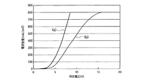
このようにして形成された電荷注入層としてモリブデン酸化物を用いた有機エレクトロルミネッセント素子(図1)(以下「モリブデン酸化物素子」とする)を直流電源に接続し、印加した電圧とその時に流れた電流値を単位面積あたりの値に換算したものの関係を表す電流密度―印加電圧曲線を図2に示す。図中縦軸は電流密度(mA/cm2)、横軸は印加電圧(V)である。またこのとき、モリブデン酸化物素子の上記電流密度と、そのときモリブデン酸化物素子から取り出された発光の強度の関係を表す発光強度―電流密度曲線を図3に示す。図中縦軸は発光強度(cd/m2)、横軸は電流密度(mA/cm2)である。図2については比較の為に図1の素子のモリブデン酸化物薄膜をPEDOTに代えた比較例1の素子(PEDOT素子とする)を同時にプロットしている。また、図3については比較の為に比較例1のPEDOT素子に加えて図1の素子からバッファ層薄膜を除いた比較例2の素子(バッファ層をもたない素子とする)を同時にプロットしている。図2、3について、図中の記号はそれぞれ、(a)及び(c)がモリブデン酸化物素子を、(b)及び(d)がPEDOT素子を、(e)がバッファ層をもたない素子を表している。 The organic electroluminescent element (FIG. 1) (hereinafter referred to as “molybdenum oxide element”) using molybdenum oxide as the charge injection layer thus formed was connected to a DC power source, the applied voltage and the time FIG. 2 shows a current density-applied voltage curve that represents the relationship between the value of the current flowing through 1 and converted to a value per unit area. In the figure, the vertical axis represents current density (mA / cm 2 ), and the horizontal axis represents applied voltage (V). At this time, FIG. 3 shows a light emission intensity-current density curve representing the relationship between the current density of the molybdenum oxide element and the intensity of light emission extracted from the molybdenum oxide element. In the figure, the vertical axis represents emission intensity (cd / m 2 ), and the horizontal axis represents current density (mA / cm 2 ). For comparison, an element of Comparative Example 1 (referred to as a PEDOT element) in which the molybdenum oxide thin film of the element of FIG. 1 is replaced with PEDOT is plotted simultaneously for comparison. For comparison, in addition to the PEDOT element of Comparative Example 1, for FIG. 3, the element of Comparative Example 2 in which the buffer layer thin film is removed from the element of FIG. 1 (the element having no buffer layer) is plotted simultaneously. ing. 2 and 3, symbols (a) and (c) are molybdenum oxide elements, (b) and (d) are PEDOT elements, and (e) is an element having no buffer layer. Represents.
図2において実施例1を示す曲線(a)と比較例1を示す曲線(b)との比較から明らかなように、本発明の実施例1のモリブデン酸化物素子の場合、立ち上がりがより早く、傾きが急峻であり、電流密度800(mA/cm2)を超えてもIV特性はほぼ直線性を維持することができることがわかる。 As apparent from the comparison between the curve (a) showing Example 1 and the curve (b) showing Comparative Example 1 in FIG. 2, in the case of the molybdenum oxide element of Example 1 of the present invention, the rise is faster, It can be seen that the slope is steep, and the IV characteristics can maintain almost linearity even if the current density exceeds 800 (mA / cm 2 ).
そして、図3において実施例1のモリブデン酸化物素子を示す曲線(c)によれば、驚くべきことに、発光強度が一桁から100000(cd/m2)まで極めて広範囲で良好な直線性を維持していることがわかる。これに対し、比較例1のPEDOT素子を示す曲線(d)によれば、比較例1の素子では発光強度―電流密度曲線が直線性を示すのはせいぜい40000(cd/m2)までであり、それ以上の発光強度を得ることはできなかった。一方比較例2のバッファ層をもたない素子では曲線(e)に示すように、電流密度に対して得られる発光強度が小さく、電流が有効に発光に寄与していないことがわかる。
これら図2および図3から、本発明の実施例1の有機エレクトロルミネッセント素子であるモリブデン酸化物素子は、幅広い発光強度範囲にわたり安定に動作し、高効率の発光強度を得ることができることがわかる。
Then, according to the curve (c) showing the molybdenum oxide element of Example 1 in FIG. 3, surprisingly, the emission intensity is extremely wide from one digit to 100,000 (cd / m 2 ) and good linearity is obtained. You can see that it is maintained. On the other hand, according to the curve (d) showing the PEDOT element of Comparative Example 1, the emission intensity-current density curve of the element of Comparative Example 1 shows linearity at most up to 40000 (cd / m 2 ). Further, the emission intensity higher than that could not be obtained. On the other hand, in the element having no buffer layer of Comparative Example 2, as shown in the curve (e), it can be seen that the emission intensity obtained with respect to the current density is small, and the current does not contribute to the emission effectively.
From these FIG. 2 and FIG. 3, the molybdenum oxide element which is the organic electroluminescent element of Example 1 of the present invention can stably operate over a wide emission intensity range and can obtain high-efficiency emission intensity. Recognize.
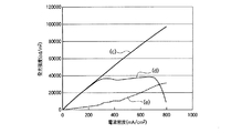
また、図4には実施例1のモリブデン酸化物素子を一定電流値(140mA/cm2)で駆動した際の発光輝度の時間変化、ならびに電流値を一定に保つ為に必要となる印加電圧の時間変化を示す。図4についても比較の為に比較例1のPEDOT素子の値を同時にプロットしている。また、両者の輝度変化の比較をより分かりやすくする為に発光輝度を評価開始時の発光輝度で規格化している。図中の記号はそれぞれ(f)が実施例1のモリブデン酸化物素子の発光輝度の変化を、(g)が比較例1のPEDOT素子の発光輝度の変化を、(h)が実施例1のモリブデン酸化物に対する印加電圧の時間変化を、(i)が比較例1のPEDOT素子に対する印加電圧の時間変化を表している。
図4においては実施例1のモリブデン酸化物素子および比較例1のPEDOT素子の経過時間と印加電圧との関係を曲線(h)、(i)で示すように、実施例1のモリブデン酸化物素子によれば長時間にわたって印加電圧の上昇もなく信頼性の高い駆動を実現することができることがあきらかである。また実施例1のモリブデン酸化物素子および比較例1のPEDOT素子の経過時間と発光強度との関係を曲線(f)、(g)で示すように、実施例1のモリブデン酸化物素子によれば長時間にわたって発光強度の低下がより少なくてすみ、より長寿命である事がわかる。
FIG. 4 shows the time variation of the emission luminance when the molybdenum oxide element of Example 1 is driven at a constant current value (140 mA / cm 2 ) and the applied voltage required to keep the current value constant. Shows time change. Also for FIG. 4, the values of the PEDOT elements of Comparative Example 1 are plotted simultaneously for comparison. In addition, in order to make the comparison of changes in luminance between the two easier to understand, the emission luminance is normalized with the emission luminance at the start of evaluation. The symbols in the figure are (f) the change in the emission brightness of the molybdenum oxide element of Example 1, (g) the change in the emission brightness of the PEDOT element of Comparative Example 1, and (h) the change in Example 1. (I) shows the time change of the applied voltage with respect to the PEDOT element of the comparative example 1, and the time change of the applied voltage with respect to molybdenum oxide.
In FIG. 4, the relationship between the elapsed time and the applied voltage of the molybdenum oxide element of Example 1 and the PEDOT element of Comparative Example 1 is shown by curves (h) and (i), and the molybdenum oxide element of Example 1 is shown. According to the above, it is apparent that highly reliable driving can be realized for a long time without increasing the applied voltage. Further, according to the molybdenum oxide element of Example 1, the relationship between the elapsed time and the emission intensity of the molybdenum oxide element of Example 1 and the PEDOT element of Comparative Example 1 is shown by curves (f) and (g). It can be seen that the emission intensity decreases less over a long time, and the life is longer.
以上のように、比較例1のPEDOT素子は比較的低い電圧から電流が流れはじめるものの、PEDOT膜の抵抗が高いために電圧を上げてもあまり電流密度が上昇しない(図2)。また、高い電圧域、即ち大電流密度の領域では飽和傾向が観察され、それ以上電流密度の増大を図ることは不可能であることがわかる。これに対して本発明の実施例1のモリブデン酸化物素子は、低い電流値から電流が流れ、かつモリブデン酸化物薄膜の抵抗が低い為にその電圧に対する上昇は速やかかつ直線的である。これはモリブデン酸化物薄膜が電荷注入層としてPEDOTを上回るきわめて良好な特性を有していることを示している。さらに、本発明の実施例1のモリブデン酸化物素子は大電流領域においてもPEDOT素子のような飽和は一切観察されない。このような特性は有機EL素子の電圧−電流密度特性として理想的なものである。モリブデン酸化物素子のこのような優れた特性は次に説明する発光強度においても同様な傾向である。 As described above, although the current starts to flow from a relatively low voltage in the PEDOT element of Comparative Example 1, the current density does not increase much even when the voltage is increased because the resistance of the PEDOT film is high (FIG. 2). In addition, a saturation tendency is observed in a high voltage region, that is, a region with a large current density, and it can be understood that the current density cannot be further increased. On the other hand, in the molybdenum oxide element of Example 1 of the present invention, the current flows from a low current value, and the resistance of the molybdenum oxide thin film is low, so the increase with respect to the voltage is quick and linear. This indicates that the molybdenum oxide thin film has very good characteristics over PEDOT as a charge injection layer. Further, the saturation of the molybdenum oxide element of Example 1 of the present invention as in the PEDOT element is not observed even in the large current region. Such characteristics are ideal as voltage-current density characteristics of the organic EL element. Such excellent characteristics of the molybdenum oxide element have the same tendency in the emission intensity described below.
図3において、PEDOT素子は、電流密度が低い領域では電流に比例して発光強度が増大していくがその傾向は速やかに頭打ちになり、図2において飽和傾向が観察された大電流領域では急激に輝度が低下している。これは高い電流密度によって劣化が急激に進行したものと考えられる。評価後の素子表面は目視でも分かる程度の変色を呈しており不可逆な変化を受けている。実際、評価後の素子を再び評価しても初期の特性は一切再現しない。また、バッファ層をもたない素子はPEDOT素子のような頭打ちの傾向こそ見られないものの、ほとんどの領域に渡ってPEDOT素子よりも発光強度が低い。これはバッファ層をもたない素子がバッファ層による電子ブロック機能を欠いているため、陰極から発光層に注入された電子の一部が発光に寄与しないままモリブデン酸化物薄膜へ抜けてしまっているためと考えられる。 In FIG. 3, in the PEDOT element, the emission intensity increases in proportion to the current in the region where the current density is low, but the tendency quickly reaches a peak, and in the large current region where the saturation tendency is observed in FIG. The brightness has dropped. This is thought to be due to the rapid progress of deterioration due to the high current density. The surface of the element after the evaluation is discolored to such an extent that it can be seen by visual observation, and has undergone an irreversible change. Actually, even if the element after evaluation is evaluated again, the initial characteristics are not reproduced at all. Moreover, although the element which does not have a buffer layer does not show the tendency of a peak like a PEDOT element, light emission intensity is lower than a PEDOT element over most areas. This is because an element that does not have a buffer layer lacks an electron blocking function by the buffer layer, so that some of the electrons injected from the cathode into the light emitting layer escape to the molybdenum oxide thin film without contributing to light emission. This is probably because of this.
これに対してモリブデン酸化物素子の優位性は明らかである、低い電流密度域でもPEDOT素子と同等、そして高い電流密度域まで電流に比例した発光強度の増大を示している。発光強度の増大は電流密度に比例しており幅広い電流域においてその発光の効率が一定であることを示している。また、評価後の素子は非常に大きな電流を流したにもかかわらずほとんど劣化は観察されず繰り返し評価を行っても同様の特性を得ることができる。 On the other hand, the superiority of the molybdenum oxide element is clear, and even in a low current density region, it is equivalent to the PEDOT element and shows an increase in emission intensity proportional to the current up to a high current density region. The increase in emission intensity is proportional to the current density, indicating that the emission efficiency is constant over a wide current range. In addition, the element after the evaluation hardly deteriorates even though a very large current flows, and the same characteristics can be obtained even if repeated evaluation is performed.
この事実は実に驚くべきことである。評価に用いられた素子の発光部分の面積は10mm2であり、その厚みは高々数百nmである。したがって、図3に示した最高輝度である800mA/cm2の時点では、この極めて小さく薄い素子に対して実に600mW以上ものエネルギーが投入されていることになる。有機EL素子は投入した電力の光への変換比率である発光効率が高いが、それでもなお熱の発生は避けられないものであって、モリブデン酸化物素子も評価後は素手では触れぬほどに高温になっている。しかも、これはガラス基板を介してのことであり、発光時の素子そのものの温度はきわめて高くなっていることが容易に推測できるものである。 This fact is amazing. The area of the light emitting portion of the element used for the evaluation is 10 mm 2 , and the thickness is at most several hundred nm. Therefore, at the time of 800 mA / cm 2 which is the maximum luminance shown in FIG. 3, energy of 600 mW or more is actually applied to this extremely small and thin element. The organic EL device has high luminous efficiency, which is the conversion ratio of input electric power to light, but heat generation is still unavoidable, and the molybdenum oxide device is too hot to be touched with bare hands after evaluation. It has become. Moreover, this is through a glass substrate, and it can be easily estimated that the temperature of the element itself during light emission is extremely high.
このように、モリブデン酸化物薄膜を電荷注入層として用いることにより優れた特性を示す理由については、明確には理解されていないが、一般的な電荷注入機構のモデルをもとに推測して解釈すると以下のようになる。以下の説明はあくまで推測に過ぎず実際の現象はまだ解明されていない。
図5はもっとも単純な有機EL素子の電荷のエネルギー状態を説明するための概略説明図である。また、図6は図5の素子構成に電荷注入層としてのPEDOT層を追加した素子の電荷のエネルギー状態を説明するための簡易説明図、図7は図5の素子構成に電荷注入層としてのモリブデン酸化物層を追加した素子の電荷のエネルギー状態を説明するための概略説明図である。
As described above, the reason why the molybdenum oxide thin film exhibits excellent characteristics by using the thin film as a charge injection layer is not clearly understood, but is presumed and interpreted based on a model of a general charge injection mechanism. Then it becomes as follows. The following explanation is only a guess, and the actual phenomenon has not been clarified yet.
FIG. 5 is a schematic explanatory diagram for explaining the energy state of the electric charge of the simplest organic EL element. 6 is a simplified explanatory diagram for explaining the energy state of the charge of the device obtained by adding a PEDOT layer as a charge injection layer to the device configuration of FIG. 5, and FIG. 7 is a diagram of the device configuration of FIG. It is a schematic explanatory drawing for demonstrating the energy state of the electric charge of the element which added the molybdenum oxide layer.
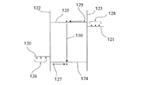
図5において、120は陽極のエネルギーレベルを示す線、121は陰極のエネルギーレベルを示す線、122は陽極と発光を司る機能層(以下発光層とする)との界面を示す線、123は陰極と発光層との界面を示す線、124は発光層の最高占有軌道(以下HOMO)、125は最低非占有軌道(以下LUMO)、126は陽極上のホール、127は発光層に注入されたホール、128は陰極上の電子、129は発光層に注入された電子、130は発光層に注入されたホール127と発光層に注入された電子129の再結合を表す線である。
In FIG. 5, 120 is a line indicating the energy level of the anode, 121 is a line indicating the energy level of the cathode, 122 is a line indicating the interface between the anode and a functional layer that controls light emission (hereinafter referred to as a light emitting layer), and 123 is the cathode. A line indicating the interface between the light emitting layer and the light emitting layer, 124 is the highest occupied orbit (hereinafter referred to as HOMO), 125 is the lowest unoccupied orbit (hereinafter referred to as LUMO), 126 is a hole on the anode, and 127 is a hole injected into the light emitting layer. , 128 are electrons on the cathode, 129 is an electron injected into the light emitting layer, and 130 is a line representing the recombination of
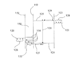
また、図6において、160は電荷注入層としてのPEDOTの部位を表し、161は陽極とPEDOT層の界面を示す線、162はPEDOT層と発光層の界面を示す線、163はPEDOT層内のホール、164はPEDOT内の準位のエネルギーレベルを示す線である。また、図7において、150は電荷注入層としてのモリブデン酸化物薄膜の部位を表し、151は陽極とモリブデン酸化物薄膜の界面を示す線、152はモリブデン酸化物薄膜と発光層の界面を示す線、153はモリブデン酸化物薄膜内のホール、154はモリブデン酸化物薄膜内の準位のエネルギーレベルを示す線である。
In FIG. 6, 160 represents a portion of PEDOT as the charge injection layer, 161 represents a line indicating the interface between the anode and the PEDOT layer, 162 represents a line indicating the interface between the PEDOT layer and the light emitting layer, and 163 represents a position in the PEDOT layer. A
説明に先立ち、図5及び6、7はあくまで簡略化、モデル化された図であることを注記する。これらは現象の説明のために最低限必要となる概念を示したものであり、実際の素子動作過程はより複雑なものであることは言うまでもない。
まず、図5を用いてもっとも単純な有機EL素子の動作について説明する。
Prior to the description, it is noted that FIGS. 5, 6 and 7 are simplified and modeled views. These show the concepts necessary for explaining the phenomenon, and it goes without saying that the actual device operation process is more complicated.
First, the simplest operation of the organic EL element will be described with reference to FIG.
有機EL素子の発光は無機LEDなどと同様にホールと電子の再結合エネルギーが光の形で解放されることで生じる。まず、図5に示すように、陽極上のホール126が発光層のHOMO124に注入され、また陰極上の電子128が発光層のLUMOに注入される。発光層に注入されたホール127及び電子129は印加された電界にしたがって発光層内を対極側に互いに逆方向に移動する。それぞれの電荷は発光層を移動する途中で一定の確率で対電荷と出会いホール-電子対、いわゆるエキシトンを生成する。エキシトンはいわばエネルギーの塊であって、このエネルギーが光の形で開放されると素子は発光を生じる。
The light emission of the organic EL element is generated when the recombination energy of holes and electrons is released in the form of light as in the case of inorganic LEDs. First, as shown in FIG. 5, holes 126 on the anode are injected into the
次に、本発明における電荷の注入について詳細に説明する。
図5において陽極のエネルギーレベルを示す線120と発光層のHOMOを示す線27に注目する。図5中におけるこれらの線の位置はそのまま電場のエネルギーを示しており、線20と線127の高さの違いはそのまま両者のエネルギーレベルの違いを示しているものとする。エネルギーレベルが異なるということはそれぞれのエネルギーレベルにあるホールは異なるエネルギーを持っていることを意味しており、一般に図5のような表現においてホールはより下方にあるものが高いエネルギーを持ち、電子はより上方にあるものが高いエネルギーを持つと定義されている。よって、発光層内のホール127は陽極上のホール126よりも高いエネルギーを持っていることになる。このとき、よりエネルギーの低い陽極上のホール126を発光層内に注入するためにはホール126とホール127の差に見合ったエネルギーを外部より与える必要があり、素子に印加される電圧の一部がこれに充当される。
Next, charge injection in the present invention will be described in detail.
In FIG. 5, attention is paid to a
上記から、キャリアの注入を行うには単にエネルギーレベルの差に相当する電圧を印加すれば良いだけであるかのように思われるが、実際には電荷注入層を用いることによって、実質的にはより低い電圧でキャリアの注入が可能になる。これは陽極、陰極いずれにおいても同様であるが、ここでは本発明に関係するところである陽極側の現象に絞ってさらに説明を加える。 From the above, it seems that it is only necessary to apply a voltage corresponding to the difference in energy level in order to inject carriers, but in practice, by using a charge injection layer, it is practically practical. Carrier injection is possible at a lower voltage. This is the same for both the anode and the cathode, but here, further explanation will be given focusing on the phenomenon on the anode side which is related to the present invention.
図6は図5に示した最も単純な有機EL素子の陽極側に電荷注入層としてのPEDOT60を設けた素子のエネルギーレベルを説明するための図である。PEDOTのもつエネルギーレベルは実質的に1つと考えてよく、それは陽極と発光層のエネルギーレベルの中間に位置するように構成されるのが一般的である。 FIG. 6 is a diagram for explaining the energy level of an element provided with PEDOT 60 as a charge injection layer on the anode side of the simplest organic EL element shown in FIG. PEDOT may be considered to have substantially one energy level, which is generally configured to be located between the energy levels of the anode and the light emitting layer.
さて、ホールの注入が行われるとき、ホールは陽極から発光層へエネルギーレベルを飛び越えて遷移するが、その遷移確率はホールの持つ平均的なエネルギーと遷移するエネルギーレベルの差に依存する。ホールの持つ平均エネルギーが大きく、エネルギーレベルの差が小さいほどより多くのホールが発光層へ注入される。このとき図5の構成の素子よりも図6の構成の素子のほうがよりホール注入が容易になるのは、PEDOTのエネルギーレベル164が陽極のエネルギーレベル120と発光層のエネルギーレベル124の中間にあるからである。図5及び6の構成の素子において同一の印加電圧、即ち同一のエネルギーがホールに与えられた場合、図6の素子では発光層のエネルギーレベル127に比較してより小さなエネルギーレベルの差のところにPEDOTのエネルギーレベル164があるためここにはきわめて容易に遷移が生じる。また、PEDOTのエネルギーレベル164に到達したホールは同様の理由で容易に発光層のエネルギーレベル124に遷移する。
Now, when holes are injected, the holes transition from the anode to the light emitting layer over the energy level, and the transition probability depends on the difference between the average energy of the holes and the transition energy level. The larger the average energy of the holes and the smaller the difference in energy level, the more holes are injected into the light emitting layer. In this case, the
この様子は擬人化して考えるとより直感的な理解を得やすいものである。即ち、人間が高い段差を登るときの様子を考えてみる。このとき、大きな段差を一気に登るよりは、中間に一段踊り場があって、二段階に分けて登ったほうが楽である。これと同じことが注入されるホールにも言えるということである。段差を登るという行為で最終的に獲得される位置エネルギーは踊場の有無にかかわらず同じであるが、そこにいたるまでの過程がより容易に行われるようになる。 This situation makes it easier to obtain a more intuitive understanding when anthropomorphic. That is, consider the situation when a human climbs a high step. At this time, it is easier to climb in two stages, with a one-step landing in the middle than to climb a large step at once. The same can be said for the injected holes. The potential energy finally obtained by the act of climbing the steps is the same regardless of the presence or absence of the landing, but the process up to that point is made easier.
さて、本実施の形態で説明しているモリブデン酸化物薄膜はPEDOTよりもより容易に電荷注入を実現できるものである。その理由を再度擬人化した類推を引用するならば、PEDOTでは踊場が設けられたのに対し、モリブデン酸化物薄膜では階段を設けたに等しくなり、より段差を登るのが楽になったと表現できる。 The molybdenum oxide thin film described in this embodiment can realize charge injection more easily than PEDOT. To quote the analogy that anthropomorphizes the reason again, it can be said that PEDOT has a dance hall, but the molybdenum oxide thin film is equivalent to a staircase, making it easier to climb the steps.
図7においてモリブデン酸化物薄膜150内には複数のエネルギーレベル154がある。これが階段として表現されたエネルギーレベルである。陽極120から発光層124にいたるエネルギーレベルがより細分化されることによりモリブデン酸化物薄膜内を移動するホール153にとって複数の互いに差の小さなエネルギーレベル153間を遷移することはきわめて容易なことになる。
In FIG. 7, there are a plurality of
では、なぜモリブデン酸化物薄膜内には、階段と表現される複数のエネルギーレベル154が生じるのであろうか。これはモリブデン酸化物薄膜の組成に由来するものと解釈できる。
So why are there
本実施の形態におけるモリブデン酸化物薄膜は、真空蒸着で作製された非晶質の薄膜である。真空蒸着時の環境は還元的雰囲気であり、その中で加熱昇華して基板上に堆積する過程でモリブデン酸化物は還元を受ける。還元を受けたモリブデン酸化物は、6価のMoO3の他に、より小さい酸化数を持ついくつかの酸化物を生じる。それらはたとえば4価のMoO2や3価のMo2O3などである。還元を受けるということは電子を受け取るということに等しいため、還元され価数が小さくなった酸化物は価数が大きな酸化物よりも電子を放しやすい状態、即ちホールを受け取りやすい状態になる。これは即ち図5から7で表現されるところのより上方のエネルギーレベルを持つということに等しい。 The molybdenum oxide thin film in this embodiment is an amorphous thin film manufactured by vacuum deposition. The environment during vacuum deposition is a reducing atmosphere, and molybdenum oxide undergoes reduction in the process of being heated and sublimated and deposited on the substrate. The reduced molybdenum oxide yields several oxides with smaller oxidation numbers in addition to hexavalent MoO 3 . They are, for example, tetravalent MoO 2 and trivalent Mo 2 O 3 . Since receiving is equivalent to receiving electrons, an oxide having a reduced valence is more likely to release electrons than an oxide having a higher valence, that is, more likely to receive holes. This is equivalent to having a higher energy level as represented in FIGS.
結果的に、図7のモリブデン酸化物のエネルギーレベル154として示しているような複数の値からなるエネルギーレベルの段状構造を生じることになる。図7のモリブデン酸化物のエネルギーレベル154は最も下方にあるエネルギーレベルが6価のものに相当し、上方に向かって価数が小さくなっていくものと解釈できる。
As a result, a step-like structure having an energy level composed of a plurality of values as shown as the
このようにして前述した階段と表現される複数のエネルギーレベル154が生じると考えられる。また、より正確には、価数の異なる酸化物によるもののほか、非晶質膜に起因するエネルギーレベルの多様化も考慮されるべきである。酸化物や窒化物で通常議論されるところのエネルギーレベルは結晶状態を基準にしたものであり、非晶質膜のようなダングリングボンドの多い複雑な構造においては、あらゆる化合物が多かれ少なかれここで説明したような複数のエネルギーレベルを持った薄膜となっていることが多い。
In this way, it is considered that a plurality of
以上説明してきたように、駆動電圧の低減をはかるとともに、後述するように陽極側での電子の抜けを防止し無効電流を低減することにより高効率化をはかることができるが、発光強度を得るためには大電流となる。大電流域においてPEDOT素子の劣化が急激に進むのは発生する熱による劣化の促進が顕著に表れることが大きな原因と考えられる。これに対し、モリブデン酸化物は無機物質であり、本質的に熱に対して非常に堅牢であることから、幅広い電流密度域にわたって安定した特性を維持しつづけるという結果が得られているものと考えられる。 As described above, the drive voltage can be reduced and, as will be described later, it is possible to achieve high efficiency by preventing the escape of electrons on the anode side and reducing the reactive current, but the emission intensity is obtained. Therefore, a large current is required. The rapid deterioration of the PEDOT element in the large current region is considered to be caused by the remarkable acceleration of the deterioration caused by the generated heat. On the other hand, molybdenum oxide is an inorganic substance and is inherently very robust to heat. Therefore, it is considered that the result of maintaining stable characteristics over a wide current density range is obtained. It is done.
このようなモリブデン酸化物の熱に対して堅牢であるという特徴は、高分子有機EL素子に応用された時にその優位性を最大限に発揮するものである。一般に低分子有機EL素子は機能層を構成する低分子有機化合物群が真空蒸着によって成膜され、基板上でアモルファス薄膜となっているという構成上、高温環境に弱い。これは、機能層が高温にさらされた時に低分子有機化合物の結晶化が進行してしまい素子の特性が劣化するからである。結晶化温度は高々百℃台であって、この結晶化温度を蒸着に必要な昇華特性を保ったままいかに高く出来るかが低分子有機EL材料の一つの課題となっている。つまり、発光層などの有機物質からなる機能層が熱に対して弱い為に、電荷注入層であるモリブデン酸化物が熱に対して堅牢であっても、その特性を活かしきれないのである。 Such a characteristic of molybdenum oxide that is robust against heat exhibits its superiority to the maximum when applied to a polymer organic EL element. In general, a low molecular organic EL element is vulnerable to a high temperature environment due to a structure in which a low molecular organic compound group constituting a functional layer is formed by vacuum deposition and is an amorphous thin film on a substrate. This is because when the functional layer is exposed to a high temperature, the crystallization of the low molecular weight organic compound proceeds and the device characteristics deteriorate. The crystallization temperature is at most 100 ° C., and how to raise the crystallization temperature while maintaining the sublimation characteristics necessary for vapor deposition is one of the problems of the low molecular organic EL material. That is, since a functional layer made of an organic material such as a light emitting layer is weak against heat, even if molybdenum oxide as a charge injection layer is robust against heat, the characteristics cannot be fully utilized.
これに対し、高分子有機EL材料は高温環境に強い。それは、高分子材料が長い分子鎖を複雑に絡み合わせることで薄膜を構成しているからである。高分子材料には明確な結晶化温度は存在せず、ガラス転移点という軟化開始温度とも言うべき指標があるのみである。さらに、多くの高分子有機EL材料では明確なガラス転移点すら観察されないことがある。つまり、別の表現をすれば、高分子有機EL材料は高温にさらされてもその絡み合った構成上、自由に動いて結晶化することが出来ないのである。このような高分子材料に一般的な特徴は、高分子材料が有機EL素子に応用される時、耐熱性という大きな優位性となって現れる。 In contrast, polymer organic EL materials are resistant to high temperature environments. This is because a polymer material forms a thin film by intertwining long molecular chains in a complicated manner. There is no clear crystallization temperature in the polymer material, and there is only an index that can be called a softening start temperature called a glass transition point. Furthermore, even a clear glass transition point may not be observed in many polymer organic EL materials. That is, in other words, the polymer organic EL material cannot move freely and crystallize due to its intertwined structure even when exposed to high temperatures. A general characteristic of such a polymer material appears as a great advantage of heat resistance when the polymer material is applied to an organic EL element.
このように、本実施例のモリブデン酸化物素子は、本質的に熱に強いモリブデン薄膜と高分子有機EL材料が組み合わさることで、大電流密度下のきわめて厳しい条件においてもなお安定な素子を構成できており、本来モリブデン酸化物に期待された良好な電荷注入特性という機能以上の大きな効果を実現している。 As described above, the molybdenum oxide element of this example is a stable element even under extremely severe conditions under a large current density by combining a heat-resistant molybdenum thin film and a polymer organic EL material. Thus, it achieves a greater effect than the function of good charge injection characteristics originally expected for molybdenum oxide.
ここで、PEDOTも高分子であるのになぜPEDOT素子は急激に劣化するのかという疑問が生じるが、これは高分子の熱に対する安定性と矛盾するものではない。 Here, although PEDOT is also a polymer, a question arises as to why the PEDOT element deteriorates rapidly. This is not inconsistent with the stability of the polymer to heat.
すでに述べたように、PEDOT素子の良好な電荷注入特性は2種類の高分子が微妙に相互作用することで得られている。大電流密度下でのPEDOT素子の急激な劣化はPEDOTを構成する高分子材料そのものが劣化しているのではなく、その物理的な構造が変化している為に生じているものである。つまり、変化は2種類の高分子材料のクーロン相互作用による緩やかな結合が外れたり、生じている相分離の状態が変化したりしているのである。PEDOTの特性はその構造によるところが大であり構造が変化するとその特性は失われてしまう。 As described above, the good charge injection characteristics of the PEDOT element are obtained by the delicate interaction of two kinds of polymers. The rapid deterioration of the PEDOT element under a large current density is caused not by the deterioration of the polymer material itself constituting PEDOT but by the change in the physical structure thereof. That is, the change is that the loose coupling due to the Coulomb interaction between the two types of polymer materials is broken, or the state of phase separation that occurs is changed. The characteristics of PEDOT depend largely on the structure. When the structure changes, the characteristics are lost.
さて、このようにモリブデン酸化物素子は優れた特性を有しているが、図2、3に示したような大電流領域での有機EL素子の駆動は現在ではまだ一般的なものではなく、一見すると実用上の意味は大きくないように思われる。しかしながら、露光ヘッドのような光源として用いる場合には高輝度のものが必要となる。また、ディスプレイで用いられるような低輝度の温和な駆動条件下においても緩慢ながら劣化が進行するのは事実であり、これは熱によって促進されることが明らかになっている。即ち、有機EL素子の劣化も他の多くの化学現象と同様活性化エネルギーに基づく反応速度論に支配されているのである。これはつまり、温和な駆動条件下での劣化は厳しい条件下で進行する現象をゆっくりと観察していることに他ならないということを示している。したがって、本実施の形態で示すところのモリブデン酸化物素子のように大電流密度という厳しい条件下でも安定でPEDOT素子よりも優れている素子は温和な駆動条件でも同様に優れた特性を持っていることは明らかである。これについては図4を用いて説明を行う。 As described above, the molybdenum oxide element has excellent characteristics, but the driving of the organic EL element in a large current region as shown in FIGS. At first glance, the practical meaning does not seem to be significant. However, when used as a light source such as an exposure head, a high-brightness one is required. Further, it is a fact that deterioration progresses slowly even under mild driving conditions with low brightness such as those used in displays, and it has become clear that this is promoted by heat. In other words, the deterioration of the organic EL element is governed by the reaction kinetics based on the activation energy as well as many other chemical phenomena. This means that deterioration under mild driving conditions is nothing but a slow observation of a phenomenon that proceeds under severe conditions. Therefore, like the molybdenum oxide element shown in the present embodiment, an element that is stable and superior to the PEDOT element even under severe conditions of high current density has excellent characteristics even under mild driving conditions. It is clear. This will be described with reference to FIG.
図4は140mA/cm2という一定の電流密度でモリブデン酸化物素子とPEDOT素子を駆動した際の発光輝度と、一定電流を流す為に必要となる印加電圧をプロットしたものである。140mA/cm2の電流を流した際には2つの素子とも15000cd/m2付近の高い輝度で発光する。この輝度はなおディスプレイなどの一般的な用途を考える際には高いものであるが、図3から分かるようにPEDOT素子も電流密度に対して比例する発光を示している領域であるので両者を比較するには好適である。
FIG. 4 is a plot of the light emission luminance when driving a molybdenum oxide element and a PEDOT element at a constant current density of 140 mA / cm 2 and the applied voltage required to flow a constant current. When a current of 140 mA / cm 2 is passed, both elements emit light with a high luminance around 15000 cd /
さて、図4からモリブデン酸化物素子がその寿命特性においてもPEDOT素子を大きく上回っていることは明らかである。また素子の状態変化の一指標となる印加電圧の時間変化もPEDOT素子と比較してモリブデン酸化物素子のそれは緩慢であり、素子の安定性を良く表しているといえる。この両者の関係はディスプレイなどで要求されるようなより温和な条件でも反転するようなことは無い。 Now, it is clear from FIG. 4 that the molybdenum oxide element greatly exceeds the PEDOT element in its life characteristics. In addition, the time change of the applied voltage, which is an index of the state change of the element, is slower than that of the PEDOT element, and it can be said that the stability of the element is well represented. The relationship between the two is not reversed even under milder conditions as required for displays and the like.
次に本発明の実施例2について説明する。
前記実施例1では発光層としてポリフルオレン系化合物を用いたが、この例では発光層4としてPPV系の材料である ポリ[2-メトキシ-5-(2-エチルヘキシロシキ)-1,4-フェンレンビニレンPoly[2-methoxy-5-(2-ethylhexyloxy)-1,4-phenylenevinylene]を用いている。この材料も実施例1と同様にたとえば日本シーベルへグナー社より購入可能である。
他の構造については前記実施例1と同様に構成した。
この場合、実施例1の場合よりもさらに発光強度を高めることができる。
Next, a second embodiment of the present invention will be described.
In Example 1, a polyfluorene compound is used as the light emitting layer. In this example, the
Other structures were the same as in Example 1.
In this case, the emission intensity can be further increased as compared with the case of Example 1.
なお前記実施例1および実施例2では、基板1としてはガラス基板を用いたが、ガラスに限定されるものではない。一般的にガラスが用いられる。本実施例でもガラス基板を採用している。基板材料としてはガラスのほかにプラスチックフィルム等をはじめとする多くの材料が提案されているが、そのいずれも本発明における基板1として採用可能である。また、光放出方向を基板と反対側の面方向とするならば、セラミック基板あるいは金属基板など遮光性の基板を用いてもよい。 In Example 1 and Example 2, a glass substrate was used as the substrate 1, but the substrate is not limited to glass. Generally, glass is used. In this embodiment, a glass substrate is also used. As the substrate material, many materials such as plastic films in addition to glass have been proposed, and any of them can be used as the substrate 1 in the present invention. Further, if the light emission direction is the surface direction opposite to the substrate, a light-shielding substrate such as a ceramic substrate or a metal substrate may be used.
基板1としては、例えば、透光性または半透光性のソーダ石灰ガラス、バリウム・ストロンチウム含有ガラス、鉛ガラス、アルミノケイ酸ガラス、ホウケイ酸ガラス、バリウムホウケイ酸ガラス、石英ガラス等の、無機酸化物ガラス、無機フッ化物ガラス、等の無機ガラス、或いは、透光性または半透光性のポリエチレンテレフタレート、ポリカーボネート、ポリメチルメタクリレート、ポリエーテルスルフォン、ポリフッ化ビニル、ポリプロピレン、ポリエチレン、ポリアクリレート、非晶質ポリオレフィン、フッ素系樹脂等の高分子フィルム等、或いは、透光性または半透光性のAs2S3、As40S10、S40Ge10等のカルコゲノイドガラス、ZnO、Nb2O、Ta2O5、SiO、Si3N4、HfO2、TiO2等の金属酸化物および窒化物等の材料、或いは、遮光性のシリコン、ゲルマニウム、炭化シリコン、ガリウム砒素、窒化ガリウム等の半導体材料、或いは、顔料等を含んだ前述の透光性基板材料、表面に絶縁処理を施した金属材料、等から適宜選択して用いることができ、複数の基板材料を積層した積層基板を用いることもできる。
Examples of the substrate 1 include inorganic oxides such as translucent or semi-translucent soda lime glass, barium / strontium-containing glass, lead glass, aluminosilicate glass, borosilicate glass, barium borosilicate glass, and quartz glass. Inorganic glass such as glass and inorganic fluoride glass, or translucent or translucent polyethylene terephthalate, polycarbonate, polymethyl methacrylate, polyether sulfone, polyvinyl fluoride, polypropylene, polyethylene, polyacrylate, amorphous Polymer films such as polyolefin and fluororesin, or translucent or semi-translucent As 2 S 3 , As 40 S 10 , S 40 Ge 10 and other chalcogenoid glasses, ZnO, Nb 2 O, ta 2 O 5, SiO, Si 3
また、陽極2としてはITOからなる電極が用いられる。ITOは導電性が高くかつ光の透過性が良い為、光取り出し側の電極として多く用いられる。前記実施例におけるITOはスパッタリングによって基板上に成膜された後、フォトリソグラフィ技術を用いて適切にパターニングされたものである。また、陽極側に光を取り出さない場合には遮光性の金属材料で構成することも可能である。電極材料としては、ITO、酸化錫(SnO2)、酸化亜鉛(ZnO)等の透明導電膜の他、クロム(Cr)、ニッケル(Ni)、銅(Cu)、錫(Sn)、タングステン(W)、金(Au)など、仕事関数の大きな金属あるいはその合金、酸化物などを用いることができる。また、安定で信頼性の高い電荷注入層を用いているため、電極としては低抵抗でかつ必要とする物性を備えた材料で構成すればよく、選択の自由度が高い。これにより電極自体の劣化を防止することができる。
As the
前記実施例において電荷注入層3として機能するモリブデン酸化物薄膜は、陽極2としてのITOがパターニングされた基板1上に真空蒸着によって成膜されている。前記実施例ではモリブデン酸化物薄膜の膜厚は20nmである。モリブデン酸化物薄膜の膜厚は特に制限は無いが、均一な膜質を得ることができれば、極端に薄いものも有効である。一般的に極端に薄い膜あるいは厚い膜は該して均一な膜質が得られなくなる場合が多いので注意が必要である。また、モリブデン酸化物薄膜は若干着色している為あまりに厚くすると光の取り出し効率が低下するが、用途によっては多少の着色はむしろ発光/非発光のコントラスト比を大きくするという効果があり好都合な場合もある。モリブデン酸化物薄膜の厚さの範囲は概ね1nmから200nmの範囲が本発明の実施に適している。
In the embodiment, the molybdenum oxide thin film functioning as the
なお、図1に示した無機酸化物からなる電荷注入層3としては前述したようにモリブデン酸化物のほかにバナジウム(V)や銅(Cu)、ニッケル(Ni)、ルテニウム(Ru)、チタン(Ti)、ジルコニウム(Zr)、タングステン(W)、イットリウム(Y)、ランタン(La)等多くの遷移金属の酸化物が同様の特性を示す。また、やや注入特性が劣るものの上記金属を含む多くの遷移金属の窒化物においても有効である。
As described above, the
また、良好な電子ブロック機能を得るために、本発明におけるバッファ層Bの電子親和力は発光層の電子親和力よりも小さいものを用いるのが望ましい。一例としてポリ[9,98-ジオクチルフルオレン−コ−N−(4-ブチルフェニル)-ジフェニルアミン)](poly[9,98−dioctylfluorene−co−N−(4−butylphenyl)−diphenylamine])などのポリフルオレン系化合物などがあげられるが、バッファ層材料は発光層材料によって制限を受けることになる。本実施例で用いられたバッファ層は発光層材料に対して十分小さな電子親和力を持っており、要件を満たしている。本実施例におけるバッファ層の膜厚は10nmであってスピンコート法によってモリブデン酸化物薄膜上に積層される。バッファ層薄膜は10nmで電子ブロックの機能を供することが出来る。バッファ層薄膜の膜厚を増すことは結果的に素子の駆動電圧を上昇させることになるため厚すぎるのは好ましいことではない。概ね50nm以下が望ましいものである。またバッファ層としては、電子ブロック機能のみならず、密着性の向上、あるいは電荷注入層と、発光層との間のエネルギー順位を持つような材料であってもよい。さらにはスピンコート法によって形成するものだけでなく、電荷注入層を真空蒸着などのドライプロセスで形成する場合にはバッファ層についても無機物で構成し、順次連続的に成膜するようにしてもよい。 In order to obtain a good electron blocking function, it is desirable to use a buffer layer B having an electron affinity smaller than that of the light emitting layer in the present invention. As an example, poly [9,98-dioctylfluorene-co-N- (4-butylphenyl) -diphenylamine)] (poly [9,98-dioctylfluorene-co-N- (4-butylphenyl) -diphenylamine]) Examples include fluorene compounds, but the buffer layer material is limited by the light emitting layer material. The buffer layer used in this example has a sufficiently small electron affinity for the light emitting layer material and satisfies the requirements. In this embodiment, the buffer layer has a thickness of 10 nm and is stacked on the molybdenum oxide thin film by a spin coating method. The buffer layer thin film can serve as an electronic block at 10 nm. Increasing the thickness of the buffer layer thin film results in an increase in the driving voltage of the device, so that it is not preferable to be too thick. A thickness of about 50 nm or less is desirable. The buffer layer may be made of a material having not only an electronic blocking function but also improved adhesion or an energy ranking between the charge injection layer and the light emitting layer. Furthermore, when the charge injection layer is formed by a dry process such as vacuum deposition as well as the one formed by spin coating, the buffer layer may also be made of an inorganic material and sequentially formed into a film. .
さらにまた、高分子有機EL材料のような特別な電気的特性を備えていない、一般にプラスチックと呼ばれているような物質、即ちポリスチレン系化合物やポリカーボネート系化合物、アクリル系化合物等を用いることも可能である。これらの物質は絶縁性が高いが、絶縁性が高いということは即ちバンドギャップが大きいということを意味し、一般にこれらプラスチックの電子親和力は小さい。もちろん絶縁性が高いので膜厚を大きくすると素子の駆動電圧が上昇することになり望ましいことではないが、膜厚を適切に設定することで本発明を実現することが出来るものである。 Furthermore, it is also possible to use a material generally called a plastic that does not have special electrical characteristics such as a polymer organic EL material, that is, a polystyrene compound, a polycarbonate compound, an acrylic compound, or the like. It is. These materials have high insulating properties, but high insulating properties mean that the band gap is large, and generally the electron affinity of these plastics is small. Of course, since the insulating property is high, increasing the film thickness increases the drive voltage of the element, which is not desirable, but the present invention can be realized by setting the film thickness appropriately.
このように、バッファ層Bとしては、高分子化合物のほか、無機物でもよく、機能としても前記実施例のように電子ブロック機能をもたなくてもよい。例えば、発光層と電荷注入層との密着性の向上を図ることのできる材料、電子のもれを抑制しうる程度にホールの注入障壁を低くするような材料であればよい。発光層がポリフルオレンのように電子輸送性の高い材料である場合には電子ブロック機能をもつバッファ層を持つことは必須であるが、PPVのように電子輸送性の低い材料である場合には、電子ブロック機能が無くてもよい場合もある。 As described above, the buffer layer B may be an inorganic substance in addition to the polymer compound, and may not have an electronic block function as in the above embodiment. For example, a material that can improve the adhesion between the light emitting layer and the charge injection layer, or a material that can lower the hole injection barrier to the extent that electron leakage can be suppressed may be used. When the light emitting layer is a material with a high electron transporting property such as polyfluorene, it is essential to have a buffer layer having an electron blocking function, but when it is a material with a low electron transporting property such as PPV. In some cases, the electronic block function may be omitted.
また、バッファ層Bについては前述したように発光層4を構成する高分子有機EL材料にあわせて適宜選択される必要がある。前記実施例では、バッファ層Bの要件は発光層4の電子親和力よりも小さな電子親和力を有することであるので、たとえば本来発光層として利用できるような化合物を用いることも可能である。したがって、化学式(I)及び化学式(II)に示したような化合物及びそれらの誘導体を含む多くの物質が選択可能である。
Further, the buffer layer B needs to be appropriately selected according to the polymer organic EL material constituting the
前記実施例1および2では、発光層4としてはスピンコートで成膜されたポリフルオレン系化合物やPPVを用い膜厚は約80nmとした。発光層4の膜厚は素子の使用条件に合わせて適宜変更されるべきものである。本発明の実施の為には50〜200nmの範囲の膜厚が適している。これについても他の薄膜と同様、あまりに膜厚が薄いと均一な膜が得られにくくなり、また膜厚が厚い場合は駆動の為に必要となる電圧が高くなりすぎるので好ましくない。
In Examples 1 and 2, as the
(実施の形態2)
図8は本発明の実施の形態2における有機EL素子の要部を示す断面図である。
(Embodiment 2)
FIG. 8 is a cross-sectional view showing the main part of the organic EL element according to
図示する有機EL素子は、前記実施の形態1と異なるのは、バッファ層Bを持たない点である。なお、他の構成について、実施の形態1において用いた図1と同様になっている。 The illustrated organic EL element is different from the first embodiment in that the buffer layer B is not provided. Other configurations are the same as those in FIG. 1 used in the first embodiment.
以上の説明において、有機EL素子は直流駆動となっているが、交流電圧または交流電流、あるいはパルス波で駆動してもよい。 In the above description, the organic EL element is driven by DC, but may be driven by AC voltage, AC current, or pulse wave.
また、有機EL素子で発光した光は基板1側から取り出すようになっているが、基板1と反対面(ここでは陰極5)側から、あるいは側面から取り出すようにしてもよい。 The light emitted from the organic EL element is extracted from the substrate 1 side, but may be extracted from the opposite surface (here, the cathode 5) side of the substrate 1 or from the side surface.
なお、本発明において、発光層としてはポリフルオレン系化合物やPPV系化合物の他にもこれらを含むコポリマー、また低分子系の発光材料を高分子骨格に化学的に結合したいわゆるペンダントタイプの高分子化合物、高分子有機EL材料と低分子有機EL材料との混合物、さらにはそれらをブレンドして用いる等適宜変更可能である。 In the present invention, as the light emitting layer, in addition to polyfluorene compounds and PPV compounds, copolymers containing these, and so-called pendant polymers in which a low molecular light emitting material is chemically bonded to a polymer skeleton are used. A compound, a mixture of a high-molecular organic EL material and a low-molecular organic EL material, or a blend of them can be used as appropriate.
ポリフルオレン及びPPVの構造はそれぞれ化学式(I)と化学式(II)に示されているが、これらを基本骨格とする誘導体はきわめて数多くのものが提案されている。たとえば、(WO9813408)あるいは(WO0228983)にPPV及びポリフルオレンの誘導体の例と詳細な説明がなされている。これらの化合物群はいずれも共役系高分子化合物といわれる物質群であり、適切なバッファ材料と組み合わせることで発光層として用いることができ、本発明の効果を実現できるものである。 The structures of polyfluorene and PPV are shown in chemical formula (I) and chemical formula (II), respectively, and a large number of derivatives having these as the basic skeleton have been proposed. For example, (WO9813408) or (WO0228983) provides examples and detailed descriptions of derivatives of PPV and polyfluorene. Any of these compound groups is a substance group called a conjugated polymer compound, and can be used as a light-emitting layer in combination with an appropriate buffer material, thereby realizing the effects of the present invention.
ここで発光層としてホール輸送性が高い材料を用いる場合はホールブロック機能を持つバッファ層を陰極側に配置することによりより発光効率を高めることができる。 Here, when a material having a high hole transport property is used as the light emitting layer, the light emission efficiency can be further increased by disposing a buffer layer having a hole blocking function on the cathode side.
いわゆるペンダント型の高分子材料は高分子骨格と従来低分子有機EL素子で用いられている発光材料を結合させることで得ることが出来、その組み合わせは膨大であるのでここでその例を一々取り上げることは現実的でない。また、高分子有機EL材料と低分子有機EL材料との混合物についてもその種類は膨大である。これらの技術の詳細は(「有機EL素子とその工業化最前線」(株)エヌティーエス)に記載されている。 The so-called pendant type polymer material can be obtained by combining a polymer skeleton and a light emitting material conventionally used in a low molecular organic EL device. Is not realistic. Moreover, the kind of the mixture of the high molecular organic EL material and the low molecular organic EL material is enormous. Details of these techniques are described in ("Organic EL devices and their industrialization front line", NTS Corporation).
なお、発光層を高分子材料(ポリマー材料)で構成することにより、大面積でも均一な膜厚で製膜できることから大面積の有機EL素子の作成が可能となる。また、発光層の熱に対する安定性が高くなるとともに、層間の界面における欠陥やピンホールの発生を抑制することができるため、安定性の高い有機EL素子を形成することができる。 In addition, since the light emitting layer is formed of a polymer material (polymer material), it is possible to form a film with a uniform film thickness even in a large area, and thus it is possible to create a large area organic EL element. In addition, the stability of the light-emitting layer to heat is increased, and defects and pinholes at the interface between layers can be suppressed, so that a highly stable organic EL element can be formed.
なお、これらの機能層(発光層、或いは、必要に応じて形成される正孔注入層、電子注入層)を高分子材料で形成する場合、スピンコーティング法や、キャスティング法や、ディッピング法や、バーコード法や、ロールコート法等の湿式成膜法であってもよい。これにより、大規模な真空装置が不要であるため、安価な設備で製膜が可能となるとともに、容易に大面積な有機EL素子の作成が可能となるとともに、有機EL素子の各層間の密着性が向上するため、素子における短絡を抑制することができ、安定性の高い有機EL素子を形成できる。 In addition, when these functional layers (light emitting layer, or hole injection layer formed as necessary, electron injection layer) are formed of a polymer material, a spin coating method, a casting method, a dipping method, A wet film forming method such as a bar code method or a roll coating method may be used. This eliminates the need for a large-scale vacuum apparatus, so that it is possible to form a film with inexpensive equipment, and it is possible to easily create a large-area organic EL element and to adhere between each layer of the organic EL element. Therefore, short circuit in the element can be suppressed, and a highly stable organic EL element can be formed.
また、カラーの表示装置などに用いる場合にはRGBの各色の発光を実現する発光層の塗り分けが必要となるが、インクジェット法などを用いることにより、容易に塗り分けを実現することができる。 In addition, when used in a color display device or the like, it is necessary to separately coat the light emitting layer that realizes light emission of each color of RGB. However, by using an ink jet method or the like, it is possible to easily realize the coloring.
また、有機エレクトロルミネッセンス素子の陰極5としては、仕事関数の低い金属もしくは合金が用いられ、Ca-Alの2層構造の他、Ba-Alの2層構造、あるいはCa、Ba、In、Mg、Ti等の金属や、Mg−Ag合金、Mg−In合金等のMg合金や、Al−Li合金、Al−Sr合金、Al−Ba合金等のAl合金等が用いられる。あるいはLiO2/AlやLiF/Al等の積層構造は陰極材料として好適である。
Further, as the
仕事関数の小さい金属を用いた光透過性の高い超薄膜を形成し、その上部に透明電極を積層することで、透明陰極を形成することもできる。この透明陰極を用いることで、いわゆるトップエミッションと呼ばれる素子構成をとることができる。 A transparent cathode can also be formed by forming an ultrathin film with high light transmittance using a metal having a small work function and laminating a transparent electrode on the ultrathin film. By using this transparent cathode, an element configuration called a so-called top emission can be taken.
このように、電荷注入層としての無機化合物とバッファ層としての高分子物質を有する高分子有機EL素子は、電流密度の広い範囲に亘って素子の発光強度、発光効率が高いレベルで維持され、また、良好な寿命特性を示す。従って、幅広い輝度の範囲にわたって安定に動作し、かつ寿命特性に優れた有機エレクトロルミネッセント素子を実現することができる。 Thus, the polymer organic EL device having the inorganic compound as the charge injection layer and the polymer material as the buffer layer is maintained at a high level of light emission intensity and light emission efficiency of the device over a wide range of current density, In addition, it exhibits good life characteristics. Therefore, it is possible to realize an organic electroluminescent device that operates stably over a wide range of luminance and has excellent lifetime characteristics.
なお、本発明の有機エレクトロルミネッセント素子を構成する各層の成膜については上記方法に限定されるものではなく、真空蒸着法、電子ビーム蒸着法、分子線エピタキシー法、スパッタリング法、反応性スパッタリング法、イオンプレーティング法、レーザーアブレーション法、熱CVD法、プラズマCVD法、MOCVD法などの真空成膜法、あるいはゾルゲル法、ラングミュア・ブロジェット法(LB法)、レイヤーバイレイヤー法、スパンコート法、インクジェット法、ディップコーティング法、スプレー法などの湿式法などから適宜選択可能であり、結果的に本発明の効果を奏効し得るように形成可能な方法であれば、いかなるものでもよいことはいうまでもない。 The film formation of each layer constituting the organic electroluminescent device of the present invention is not limited to the above method, but vacuum deposition method, electron beam deposition method, molecular beam epitaxy method, sputtering method, reactive sputtering. Method, ion plating method, laser ablation method, thermal CVD method, plasma CVD method, MOCVD method, etc., or sol-gel method, Langmuir-Blodget method (LB method), layer-by-layer method, span coat method Any method may be used as long as it can be appropriately selected from wet methods such as an inkjet method, a dip coating method, and a spray method, and can be formed so that the effects of the present invention can be obtained as a result. Not too long.
本発明にかかる有機EL素子は、幅広い輝度の範囲にわたって安定に動作し、かつ寿命特性に優れているのでフラットパネルディスプレイや表示素子、光源などを含む広範な応用において有用である。 The organic EL device according to the present invention operates stably over a wide range of luminance and has excellent life characteristics, and thus is useful in a wide range of applications including flat panel displays, display devices, light sources, and the like.
1 基板
2 陽極
3 電荷注入層
B バッファ層
4 発光層
5 陰極
DESCRIPTION OF SYMBOLS 1
Claims (21)
前記機能層は少なくとも1種類の高分子物質からなる発光機能を有した層と、少なくとも1種類の無機酸化物からなる電荷注入層とを含む有機エレクトロルミネッセント素子。 Comprising at least one set of electrodes and a plurality of functional layers formed between the electrodes;
The functional layer is an organic electroluminescent device including a layer having a light emitting function made of at least one polymer substance and a charge injection layer made of at least one inorganic oxide.
前記機能層は少なくとも1種類のバッファ層を含む有機エレクトロルミネッセント素子。 The organic electroluminescent device according to claim 1,
The functional layer is an organic electroluminescent device including at least one buffer layer.
前記バッファ層が高分子層で構成される有機エレクトロルミネッセント素子。 The organic electroluminescent device according to claim 1 or 2,
An organic electroluminescent device in which the buffer layer is composed of a polymer layer.
前記バッファ層が有機溶媒を含む有機エレクトロルミネッセント素子。 An organic electroluminescent device according to any one of claims 1 to 3,
An organic electroluminescent device in which the buffer layer contains an organic solvent.
前記バッファ層の電子親和力をあらわすエネルギー値の絶対値が前記発光機能を有した層の電子親和力をあらわすエネルギー値の絶対値よりも小さい有機エレクトロルミネッセント素子。 An organic electroluminescent device according to any one of claims 1 to 4,
An organic electroluminescent element, wherein an absolute value of an energy value representing an electron affinity of the buffer layer is smaller than an absolute value of an energy value representing an electron affinity of the layer having the light emitting function.
前記発光機能を有した層がフルオレン環を含む高分子化合物を含む有機エレクトロルミネッセント素子。 An organic electroluminescent device according to any one of claims 1 to 5,
The organic electroluminescent element in which the layer having the light emitting function contains a polymer compound containing a fluorene ring.
前記発光機能を有した層が下記一般式(I)で表されるポリフルオレン及びその誘導体(R1、R2はそれぞれ置換基を表す)を含むことを特徴とする有機エレクトロルミネッセント素子。
The organic electroluminescent element characterized in that the layer having the light emitting function contains polyfluorene represented by the following general formula (I) and derivatives thereof (R1 and R2 each represent a substituent).
前記発光機能を有した層がフェニレンビニレン基を含む有機エレクトロルミネッセント素子。 An organic electroluminescent device according to any one of claims 1 to 5,
The organic electroluminescent element in which the layer having the light emitting function contains a phenylene vinylene group.
前記発光機能を有した層が下記一般式(II)で表されるポリフェニレンビニレン及びその誘導体(R3、R4はそれぞれ置換基を表す)を含むことを特徴とする有機エレクトロルミネッセント素子。
The organic electroluminescent element characterized in that the layer having a light emitting function contains polyphenylene vinylene represented by the following general formula (II) and derivatives thereof (R3 and R4 each represent a substituent).
前記電荷注入層が遷移金属の酸化物を含む有機エレクトロルミネッセント素子。 An organic electroluminescent device according to any one of claims 1 to 9,
An organic electroluminescent device in which the charge injection layer includes an oxide of a transition metal.
前記電荷注入層がモリブデンまたはバナジウムの酸化物を含むことを特徴とする有機エレクトロルミネッセント素子。 The organic electroluminescent device according to claim 11,
An organic electroluminescent device, wherein the charge injection layer contains an oxide of molybdenum or vanadium.
前記電荷注入層が銅酸化物を含むことを特徴とする有機エレクトロルミネッセント素子。 The organic electroluminescent device according to claim 11,
The organic electroluminescent device, wherein the charge injection layer contains a copper oxide.
前記電荷注入層が希土類元素の酸化物を含むことを特徴とする有機エレクトロルミネッセント素子。 The organic electroluminescent device according to claim 1,
An organic electroluminescent device, wherein the charge injection layer contains an oxide of a rare earth element.
前記電荷注入層がランタンの酸化物を含むことを特徴とする有機エレクトロルミネッセント素子。 The organic electroluminescent device according to claim 14, wherein
The organic electroluminescent device, wherein the charge injection layer contains an oxide of lanthanum.
前記電荷注入層がアルミニウムの酸化物を含むことを特徴とする有機エレクトロルミネッセント素子。 The organic electroluminescent device according to claim 1,
The organic electroluminescent device, wherein the charge injection layer contains an oxide of aluminum.
前記電荷注入層が酸化シリコンを含むことを特徴とする有機エレクトロルミネッセント素子。 The organic electroluminescent device according to claim 1,
The organic electroluminescent device, wherein the charge injection layer contains silicon oxide.
前記バッファ層は、ホール注入側に配置された電荷注入層と発光機能を有した層との間に配置される有機エレクトロルミネッセント素子。 An organic electroluminescent device according to any one of claims 2 to 17,
The buffer layer is an organic electroluminescent device disposed between a charge injection layer disposed on the hole injection side and a layer having a light emitting function.
前記一組の電極のうちの一方の電極である陽極は透光性基板上に形成されており、
前記電荷注入層は、前記陽極上に形成されたホール注入層と、
前記発光機能を有した層を介して前記ホール注入層に対向するように、前記発光機能を有した層の上に形成された電子注入層とで構成され、
前記電子注入層上には前記一組の電極のうち他方の電極である陰極が形成された有機エレクトロルミネッセント素子。 The organic electroluminescent device according to claim 1,
The anode which is one electrode of the set of electrodes is formed on a translucent substrate,
The charge injection layer includes a hole injection layer formed on the anode;
An electron injection layer formed on the layer having the light emitting function so as to face the hole injection layer through the layer having the light emitting function;
An organic electroluminescent element in which a cathode which is the other electrode of the set of electrodes is formed on the electron injection layer.
前記機能層は少なくとも1種類の高分子物質からなる発光機能を有した層と、少なくとも1種類の無機酸化物からなる電荷注入層とを含む有機エレクトロルミネッセント素子の製造方法であって、
前記発光機能を有した層は、高分子化合物溶液を供給することによって形成される有機エレクトロルミネッセント素子の製造方法。 Comprising at least one set of electrodes and a plurality of functional layers formed between the electrodes;
The functional layer is a method for manufacturing an organic electroluminescent device including a layer having a light emitting function made of at least one polymer substance and a charge injection layer made of at least one inorganic oxide,
The layer having a light emitting function is a method for producing an organic electroluminescent element formed by supplying a polymer compound solution.
透光性基板表面に、電極を形成する工程と、
前記電極上に真空成膜法により無機酸化物層からなる電荷注入層を形成する工程と、
前記電荷注入層上に高分子化合物溶液を供給することによってバッファ層を形成する工程と、
前記バッファ層上に高分子化合物溶液を供給することによって少なくとも1種類の高分子物質からなる発光機能を有した層を形成する工程と、
前記発光機能を有した層上に電極を形成する工程とを含む有機エレクトロルミネッセント素子の製造方法。 It is a manufacturing method of the organic electroluminescent element according to claim 20,
Forming an electrode on the surface of the translucent substrate;
Forming a charge injection layer made of an inorganic oxide layer on the electrode by a vacuum film formation method;
Forming a buffer layer by supplying a polymer compound solution on the charge injection layer;
Forming a layer having a light-emitting function composed of at least one polymer substance by supplying a polymer compound solution onto the buffer layer;
Forming an electrode on the layer having a light emitting function, and a method for producing an organic electroluminescent element.
前記発光機能を有した層を形成する工程は、塗布法である有機エレクトロルミネッセント素子の製造方法。 It is a manufacturing method of the organic electroluminescent element according to claim 20,
The step of forming the layer having a light emitting function is a method for manufacturing an organic electroluminescent element, which is a coating method.
Priority Applications (1)
| Application Number | Priority Date | Filing Date | Title |
|---|---|---|---|
| JP2004301621A JP2006114759A (en) | 2004-10-15 | 2004-10-15 | Organic electroluminescent element and its manufacturing method |
Applications Claiming Priority (1)
| Application Number | Priority Date | Filing Date | Title |
|---|---|---|---|
| JP2004301621A JP2006114759A (en) | 2004-10-15 | 2004-10-15 | Organic electroluminescent element and its manufacturing method |
Publications (2)
| Publication Number | Publication Date |
|---|---|
| JP2006114759A true JP2006114759A (en) | 2006-04-27 |
| JP2006114759A5 JP2006114759A5 (en) | 2007-11-29 |
Family
ID=36383016
Family Applications (1)
| Application Number | Title | Priority Date | Filing Date |
|---|---|---|---|
| JP2004301621A Withdrawn JP2006114759A (en) | 2004-10-15 | 2004-10-15 | Organic electroluminescent element and its manufacturing method |
Country Status (1)
| Country | Link |
|---|---|
| JP (1) | JP2006114759A (en) |
Cited By (12)
| Publication number | Priority date | Publication date | Assignee | Title |
|---|---|---|---|---|
| JP2008182164A (en) * | 2007-01-26 | 2008-08-07 | Semiconductor Energy Lab Co Ltd | Light-emitting element and light-emitting device |
| JP2009021575A (en) * | 2007-06-14 | 2009-01-29 | Semiconductor Energy Lab Co Ltd | Light-emitting element, light-emitting device, electronic equipment, and light-emitting element manufacturing method |
| US7723916B2 (en) | 2007-03-23 | 2010-05-25 | Toppan Printing Co., Ltd. | Organic electroluminescence element and display using the same |
| US7990049B2 (en) | 2007-09-03 | 2011-08-02 | Canon Kabushiki Kaisha | Organic electroluminescent device and production method of the device, and display apparatus |
| US8183764B2 (en) * | 2008-03-26 | 2012-05-22 | Toppan Printing Co., Ltd. | Organic electroluminescence element, manufacturing method for an organic electroluminescence element and display unit |
| WO2013157451A1 (en) * | 2012-04-16 | 2013-10-24 | 日本放送協会 | Organic electroluminescent element and method for manufacturing same |
| JP2013239691A (en) * | 2012-04-16 | 2013-11-28 | Nippon Hoso Kyokai <Nhk> | Organic electroluminescent element and method of manufacturing the same |
| JP2014049697A (en) * | 2012-09-03 | 2014-03-17 | Nippon Hoso Kyokai <Nhk> | Organic electroluminescent element |
| CN104009167A (en) * | 2013-02-26 | 2014-08-27 | 海洋王照明科技股份有限公司 | Organic electroluminescent device and preparation method |
| JP2014168014A (en) * | 2013-02-28 | 2014-09-11 | Nippon Hoso Kyokai <Nhk> | Organic electroluminescent element |
| CN104247073A (en) * | 2012-04-16 | 2014-12-24 | 日本放送协会 | Organic electroluminescent element and method for manufacturing same |
| CN108183173A (en) * | 2017-12-14 | 2018-06-19 | 中国科学院广州能源研究所 | It is a kind of based on light emitting diode with quantum dots for mixing yttrium zinc oxide electron transfer layer and preparation method thereof |
-
2004
- 2004-10-15 JP JP2004301621A patent/JP2006114759A/en not_active Withdrawn
Cited By (14)
| Publication number | Priority date | Publication date | Assignee | Title |
|---|---|---|---|---|
| JP2008182164A (en) * | 2007-01-26 | 2008-08-07 | Semiconductor Energy Lab Co Ltd | Light-emitting element and light-emitting device |
| US7723916B2 (en) | 2007-03-23 | 2010-05-25 | Toppan Printing Co., Ltd. | Organic electroluminescence element and display using the same |
| JP2009021575A (en) * | 2007-06-14 | 2009-01-29 | Semiconductor Energy Lab Co Ltd | Light-emitting element, light-emitting device, electronic equipment, and light-emitting element manufacturing method |
| US7990049B2 (en) | 2007-09-03 | 2011-08-02 | Canon Kabushiki Kaisha | Organic electroluminescent device and production method of the device, and display apparatus |
| US8183764B2 (en) * | 2008-03-26 | 2012-05-22 | Toppan Printing Co., Ltd. | Organic electroluminescence element, manufacturing method for an organic electroluminescence element and display unit |
| JP2013239691A (en) * | 2012-04-16 | 2013-11-28 | Nippon Hoso Kyokai <Nhk> | Organic electroluminescent element and method of manufacturing the same |
| WO2013157451A1 (en) * | 2012-04-16 | 2013-10-24 | 日本放送協会 | Organic electroluminescent element and method for manufacturing same |
| CN104247073A (en) * | 2012-04-16 | 2014-12-24 | 日本放送协会 | Organic electroluminescent element and method for manufacturing same |
| KR20150008085A (en) * | 2012-04-16 | 2015-01-21 | 닛폰 호소 교카이 | Organic electroluminescent element and method for manufacturing same |
| KR102171425B1 (en) * | 2012-04-16 | 2020-10-29 | 닛폰 호소 교카이 | Organic electroluminescent element and method for manufacturing same |
| JP2014049697A (en) * | 2012-09-03 | 2014-03-17 | Nippon Hoso Kyokai <Nhk> | Organic electroluminescent element |
| CN104009167A (en) * | 2013-02-26 | 2014-08-27 | 海洋王照明科技股份有限公司 | Organic electroluminescent device and preparation method |
| JP2014168014A (en) * | 2013-02-28 | 2014-09-11 | Nippon Hoso Kyokai <Nhk> | Organic electroluminescent element |
| CN108183173A (en) * | 2017-12-14 | 2018-06-19 | 中国科学院广州能源研究所 | It is a kind of based on light emitting diode with quantum dots for mixing yttrium zinc oxide electron transfer layer and preparation method thereof |
Similar Documents
| Publication | Publication Date | Title |
|---|---|---|
| JP2005203339A (en) | Organic electroluminescent element and its manufacturing method | |
| JP2005203340A (en) | Organic electroluminescent element | |
| US7785718B2 (en) | Organic electroluminescent device and method for manufacturing the same | |
| US20090160325A1 (en) | Organic electroluminescent device and method for manufacturing the same | |
| KR101357045B1 (en) | Tunable Light Emitting Diode using Graphene conjugated Metal oxide semiconductor-Graphene core-shell Quantum dots and its fabrication process thereof | |
| KR100642431B1 (en) | Quantum Dot Light Emitting Diode Comprising Inorganic Electron Transport Layer | |
| JP4736890B2 (en) | Organic electroluminescence device | |
| JP2005251587A (en) | Organic el device | |
| KR101690806B1 (en) | Ink-jet printing ink for organic electroluminescent element, and process for production of organic electroluminescent element | |
| JP2017516317A (en) | Electroluminescence device | |
| WO2007091548A1 (en) | Organic electroluminescent element | |
| JP2009060012A (en) | Organic field-effect element and manufacturing method therefor, and display device | |
| JP5017820B2 (en) | ELECTROLUMINESCENT DEVICE AND METHOD FOR MANUFACTURING THE SAME | |
| TW200950175A (en) | Organic electroluminescence device and method of fabricating the same, and illuminator | |
| JP2006114759A (en) | Organic electroluminescent element and its manufacturing method | |
| KR100769946B1 (en) | Organic electroluminesecnt device capable of driving in low voltage | |
| JP2008016868A (en) | Organic electroluminescent element and method of manufacturing the same | |
| US20080012480A1 (en) | Organic electroluminescent device and method for manufacturing the same | |
| JP2004171951A (en) | Anode for organic semiconductor device | |
| JP4815118B2 (en) | Organic electroluminescent device and manufacturing method thereof | |
| KR100888148B1 (en) | Organic Electro luminescence Device and fabrication method of thereof | |
| JP2009088419A (en) | Electroluminescent device and its manufacturing method, and display device | |
| JP2006114743A (en) | Organic electroluminescent element and its manufacturing method | |
| JP2006114754A (en) | Organic electroluminescent element and its manufacturing method | |
| JP2006114758A (en) | Display device and its manufacturing method |
Legal Events
| Date | Code | Title | Description |
|---|---|---|---|
| A521 | Request for written amendment filed |
Free format text: JAPANESE INTERMEDIATE CODE: A523 Effective date: 20071012 |
|
| A621 | Written request for application examination |
Free format text: JAPANESE INTERMEDIATE CODE: A621 Effective date: 20071012 |
|
| RD02 | Notification of acceptance of power of attorney |
Free format text: JAPANESE INTERMEDIATE CODE: A7422 Effective date: 20071113 |
|
| RD04 | Notification of resignation of power of attorney |
Free format text: JAPANESE INTERMEDIATE CODE: A7424 Effective date: 20071120 |
|
| A761 | Written withdrawal of application |
Free format text: JAPANESE INTERMEDIATE CODE: A761 Effective date: 20090624 |