JP2006114709A - ESD protection circuit - Google Patents
ESD protection circuit Download PDFInfo
- Publication number
- JP2006114709A JP2006114709A JP2004300819A JP2004300819A JP2006114709A JP 2006114709 A JP2006114709 A JP 2006114709A JP 2004300819 A JP2004300819 A JP 2004300819A JP 2004300819 A JP2004300819 A JP 2004300819A JP 2006114709 A JP2006114709 A JP 2006114709A
- Authority
- JP
- Japan
- Prior art keywords
- power supply
- transistor
- peripheral
- output transistor
- circuit
- Prior art date
- Legal status (The legal status is an assumption and is not a legal conclusion. Google has not performed a legal analysis and makes no representation as to the accuracy of the status listed.)
- Granted
Links
Images
Landscapes
- Semiconductor Integrated Circuits (AREA)
- Metal-Oxide And Bipolar Metal-Oxide Semiconductor Integrated Circuits (AREA)
- Logic Circuits (AREA)
Abstract
【課題】 半導体装置をESD(サージ)からゲート絶縁膜を保護する保護機能を備えた半導体装置のための保護装置を提供する。
【解決手段】 分割されたGNDライン及び電源ラインを有するESD保護回路内における出力トランジスタ(6a、6b)のVCC端子13側又はGND端子12側の電極とゲート電極との間に、保護トランジスタを接続し、さらに、該保護トランジスタ(30a、30b)のゲート電極側に遅延回路(31a、31b)及び抵抗(32a、32b)を設けることにより、負方向の電圧が出力トランジスタ(6a、6b)に印加された場合であっても、出力トランジスタ(6a、6b)のゲート電極に電圧を印加し、ドレイン電流を放電し、ゲート絶縁膜の破壊を防止できる。
【選択図】 図1PROBLEM TO BE SOLVED: To provide a protection device for a semiconductor device having a protection function for protecting a gate insulating film from ESD (surge).
A protection transistor is connected between an electrode on the VCC terminal 13 side or a GND terminal 12 side and a gate electrode of an output transistor (6a, 6b) in an ESD protection circuit having a divided GND line and power supply line. Furthermore, by providing a delay circuit (31a, 31b) and a resistor (32a, 32b) on the gate electrode side of the protection transistor (30a, 30b), a negative voltage is applied to the output transistor (6a, 6b). Even in such a case, voltage can be applied to the gate electrodes of the output transistors (6a, 6b), the drain current can be discharged, and the gate insulating film can be prevented from being broken.
[Selection] Figure 1
Description
本発明は、半導体装置をサージからゲート絶縁膜を保護する保護機能を備えた半導体装置のための保護装置に関する。 The present invention relates to a protection device for a semiconductor device having a protection function for protecting a gate insulating film from a surge of the semiconductor device.
従来の半導体装置は、外部からのESD(サージ)によりゲート絶縁膜が静電気破壊されることがある。静電気破壊を防止するため、半導体装置の外部出力端子または外部入力端子のセル内に保護トランジスタが設けられている。しかし、半導体装置の微細化に伴い、外部入出力端子の静電気破壊耐性が低下し、大きな問題となってきている。 In the conventional semiconductor device, the gate insulating film may be electrostatically broken due to ESD (surge) from the outside. In order to prevent electrostatic breakdown, a protection transistor is provided in the external output terminal or the cell of the external input terminal of the semiconductor device. However, with the miniaturization of semiconductor devices, the resistance to electrostatic breakdown of external input / output terminals has been reduced, which has become a serious problem.
一般的に、保護トランジスタには、MOS形トランジスタを用い、MOS形トランジスタに電流集中させることにより、ブレークダウンを起こし、サージによるデート絶縁膜の静電気破壊を防止している。 In general, a MOS transistor is used as a protection transistor, and current is concentrated on the MOS transistor, thereby causing breakdown and preventing electrostatic breakdown of the date insulating film due to surge.
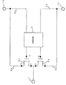
図3に従来のESD保護回路の回路図を示す。複数のFETで構成された内部回路5を有し、その出力側には、出力トランジスタ(Pチャンネル型トランジスタ)6a及び出力トランジスタ(Nチャンネル型トランジスタ)6bのゲート電極Gがそれぞれ接続されている。内部回路5は、内部回路用GNDライン9bを介してGND端子12に接続されると共に、内部回路用電源ライン8bを介して電源電圧VDD印可用の電源端子13に接続されている。出力トランジスタ6bのドレイン電極Dは、外部出力端子7に接続され、そのソース電極Sが周辺GNDライン9aに接続され、該周辺GNDライン9aはGND端子12に接続されている。出力トランジスタ6aのドレイン電極Dは、外部出力端子7に接続され、そのソース電極Sが周辺電源ライン8aに接続され、該周辺電源ライン8aは電源端子13に接続されている。
FIG. 3 shows a circuit diagram of a conventional ESD protection circuit. The
GND端子12には、内部回路用GNDライン9bを介して内部回路5が接続され、さらに内部回路5は内部回路用電源ライン8bを介して電源端子13に接続されている。出力トランジスタ6a、6bは、内部回路5の出力によってゲート制御される。
The
特許文献1には、内部回路用電源ライン及び内部回路用GNDラインと周辺電源ライン及び周辺GNDラインとの両方またはいずれか一方がチップ配線パターン上、分割された半導体集積回路において、外部GND端子あるいは外部電源端子に対して外部出力端子あるいは外部入出力端子に静電気サージが流入すると、それらに接続された出力トランジスタのゲート絶縁膜の破壊現象の発生を防止できる半導体集積回路が提案されている。
しかし、上記の発明は、以下の問題を有している。 However, the above invention has the following problems.
ブレークダウンは、負方向電圧が印加されている保護トランジスタの電圧が降伏電圧に達しないと発生しないため、降伏電圧に達するまで印加される電圧によるストレスによりゲート絶縁膜の破壊が発生する。保護トランジスタのゲートの長さを短くすることにより降伏電圧を低下させることができるが、ゲートの長さを変化させるのは、回路設計上、困難である。 Since breakdown does not occur unless the voltage of the protection transistor to which the negative voltage is applied reaches the breakdown voltage, the gate insulating film is destroyed by stress due to the voltage applied until the breakdown voltage is reached. Although the breakdown voltage can be lowered by shortening the gate length of the protection transistor, it is difficult in terms of circuit design to change the gate length.
具体的には、図3において、ESD保護回路には4つの印可パターン、VCC13の電圧を正方向に大きくした場合(以下、VCC+とする)、VCC13の電圧を負方向に多くした場合(以下、VCC−とする)、GND12の電圧を正方向に大きくした場合(以下、GND+とする)、GND12の電圧を負方向に大きくした場合(以下、GND−とする)がある。VCC+とGND−とが印加された場合、各出力トランジスタには正方向の電圧が印加されるため、ドレイン電流が急激に増加するブレークダウンは生じないため、ゲート絶縁膜の破壊に対する耐性が高い。 Specifically, in FIG. 3, the ESD protection circuit includes four applied patterns, when the voltage of VCC13 is increased in the positive direction (hereinafter referred to as VCC +), and when the voltage of VCC13 is increased in the negative direction (hereinafter, referred to as VCC). VCC−), when GND12 voltage is increased in the positive direction (hereinafter referred to as GND +), and GND12 voltage is increased in the negative direction (hereinafter referred to as GND−). When VCC + and GND− are applied, since a positive voltage is applied to each output transistor, a breakdown in which the drain current increases rapidly does not occur, and thus the resistance against breakdown of the gate insulating film is high.
しかし、VCC−とGND+とが印加された場合、各出力トランジスタには負方向の電圧が印加され、ドレイン電流が流れず、降伏電圧に達したとき、電流が急激に増加し、ゲート絶縁膜の破壊に対する耐性が低い。この負方向の電圧が約±10V(降伏電圧)に達すると、ブレークダウンが発生する。つまり、ブレークダウンが起こるまでのドレイン−ソース間の電位、及びドレイン−ゲート間の電位が±10V程度に達すると、ゲート絶縁膜の破壊が発生する。 However, when VCC− and GND + are applied, a negative voltage is applied to each output transistor, the drain current does not flow, and when the breakdown voltage is reached, the current increases rapidly, and the gate insulating film Low resistance to destruction. When this negative voltage reaches about ± 10 V (breakdown voltage), breakdown occurs. That is, when the drain-source potential and the potential between the drain and the gate until breakdown occurs reach about ± 10 V, the gate insulating film is broken.
また、VCC−が印加された場合、出力トランジスタ6aは、負方向の電圧となり、電流が急激に増加するブレークダウンが発生し、ゲート絶縁膜の破壊に対する耐性が低くなる。一方、出力トランジスタ6bには、正方向の電圧が印加され、電流が急激に増加するブレークダウンは生じないため、ゲート絶縁膜の破壊に対する耐性は高い。 Further, when VCC− is applied, the output transistor 6a becomes a negative voltage, a breakdown in which the current rapidly increases occurs, and the resistance to the breakdown of the gate insulating film is lowered. On the other hand, a positive voltage is applied to the output transistor 6b, and a breakdown in which the current increases rapidly does not occur. Therefore, the output transistor 6b has high resistance to the breakdown of the gate insulating film.
また、GND+が印加された場合、出力トランジスタ6bは、負方向の電圧となり、電流が急激に増加するブレークダウンが発生し、ゲート絶縁膜の破壊に対する耐性が低くなる。一方、出力トランジスタ6aには、正方向の電圧が印加され、電流が急激に増加するブレークダウンは生じないため、ゲート絶縁膜の破壊に対する耐性は高い。 In addition, when GND + is applied, the output transistor 6b becomes a negative voltage, a breakdown in which the current rapidly increases occurs, and resistance to breakdown of the gate insulating film is lowered. On the other hand, a positive voltage is applied to the output transistor 6a, and a breakdown in which the current increases rapidly does not occur. Therefore, the output transistor 6a is highly resistant to the breakdown of the gate insulating film.
特許文献1記載の半導体集積回路は、分割されたGNDライン及び電源ラインを有する半導体集積回路内における出力トランジスタの周辺電源ライン側又は周辺GNDライン側の電極とゲート電極との間に、保護回路を接続することにより、外部出力端子または外部入出力端子に静電気サージが流入し、出力トランジスタがブレークダウンを発生したとき、保護回路を動作させ、該出力トランジスタの周辺電源ライン側または周辺GNDライン側の電極とゲート電極との間の電位差を減少させている。しかし、該出力トランジスタがブレークダウンするまでサージによりゲート絶縁膜が破壊されることがある。
In the semiconductor integrated circuit described in
そこで、本発明は、分割されたGNDライン及び電源ラインを有するESD保護回路内における出力トランジスタのVCC端子側又はGND端子側の電極とゲート電極との間に、保護トランジスタを接続し、さらに、該保護トランジスタのゲート電極側に遅延回路及び抵抗を設けることにより、負方向の電圧が出力トランジスタに印加された場合であっても、出力トランジスタのゲート電極に電圧を印加し、ドレイン電流を放電し、ゲート絶縁膜の破壊を防止できるESD保護回路を提供することを目的としている。 Therefore, the present invention connects a protection transistor between the VCC terminal side or GND terminal side electrode of the output transistor and the gate electrode in the ESD protection circuit having the divided GND line and power supply line, and By providing a delay circuit and a resistor on the gate electrode side of the protection transistor, even when a negative voltage is applied to the output transistor, a voltage is applied to the gate electrode of the output transistor, and the drain current is discharged. An object of the present invention is to provide an ESD protection circuit capable of preventing the gate insulating film from being broken.
請求項1記載の発明は、複数のFETで構成された内部回路と、前記内部回路に電源電圧を供給する内部回路用電源ライン及び内部回路用グランドラインと、前記内部回路の出力によってゲート制御され該内部回路の出力に応じた信号を外部出力端子又は外部入出力端子へ出力する出力トランジスタと、前記出力トランジスタに接続され前記出力トランジスタに電源電圧を印加する周辺電源ライン及び周辺グランドラインとを備え、前記内部回路用電源ライン及び内部回路用グランドラインと前記周辺電源ライン及び周辺グランドラインとの両方又はいずれか一方がチップ配線上、分割されたESD保護回路において、前記出力トランジスタのゲート電極と、前記周辺電源ライン又は前記周辺グランドラインとの間に前記出力トランジスタがブレークダウンする前にその両電極間の電位差を減少させる保護回路と、前記保護回路は、前記出力トランジスタのゲート電極と前記周辺電源ライン又は前記周辺グランドラインとの間に接続された前記保護トランジスタと、前記保護トランジスタのゲート電極と前記周辺電源ライン又は前記周辺グランドラインとの間に遅延回路及び抵抗とを有することを特徴とする。
The invention according to
請求項2記載の発明は、請求項1記載のESD保護回路において、前記抵抗が前記遅延回路と前記周辺電源ライン又は前記周辺グランドラインとの間に接続されていることを特徴とする。 According to a second aspect of the present invention, in the ESD protection circuit according to the first aspect, the resistor is connected between the delay circuit and the peripheral power supply line or the peripheral ground line.
請求項3記載の発明は、請求項1記載のESD保護回路において、前記抵抗が前記保護トランジスタのゲート電極と前記遅延回路との間に接続されていることを特徴とする。 According to a third aspect of the present invention, in the ESD protection circuit according to the first aspect, the resistor is connected between a gate electrode of the protection transistor and the delay circuit.
請求項4記載の発明は、複数の第1の抵抗と、前記抵抗に電源電圧を供給する抵抗用電源ライン及び抵抗用グランドラインと、前記抵抗の出力によってゲート制御され該抵抗の出力に応じた信号を外部出力端子又は外部入出力端子へ出力する出力トランジスタと、前記出力トランジスタに接続され前記出力トランジスタに電源電圧を印加する周辺電源ライン及び周辺グランドラインとを備え、前記抵抗用電源ライン及び抵抗用グランドラインと前記周辺電源ライン及び周辺グランドラインとの両方又はいずれか一方がチップ配線上、分割されたESD保護回路において、前記出力トランジスタのゲート電極と、前記周辺電源ライン又は前記周辺グランドラインとの間に前記出力トランジスタがブレークダウンする前にその両電極間の電位差を減少させる保護回路と、前記保護回路は、前記出力トランジスタのゲート電極と前記周辺電源ライン又は前記周辺グランドラインとの間に接続された前記保護トランジスタと、前記保護トランジスタのゲート電極と前記周辺電源ライン又は前記周辺グランドラインとの間に遅延回路及び第2の抵抗とを有することを特徴とする。 According to a fourth aspect of the present invention, a plurality of first resistors, a resistor power supply line for supplying a power supply voltage to the resistors, a resistor ground line, and gates are controlled by the outputs of the resistors in accordance with the outputs of the resistors. An output transistor that outputs a signal to an external output terminal or an external input / output terminal; and a peripheral power supply line and a peripheral ground line that are connected to the output transistor and apply a power supply voltage to the output transistor; In the ESD protection circuit in which the ground line and / or the peripheral power line and / or the peripheral ground line are divided on the chip wiring, the gate electrode of the output transistor, the peripheral power line, or the peripheral ground line Before the output transistor breaks down. A protection circuit to be reduced, the protection circuit including the protection transistor connected between the gate electrode of the output transistor and the peripheral power supply line or the peripheral ground line, and the gate electrode of the protection transistor and the peripheral power supply line. Alternatively, a delay circuit and a second resistor are provided between the peripheral ground line and the peripheral ground line.
請求項5記載の発明は、請求項4記載のESD保護回路において、前記第2の抵抗が前記遅延回路と前記周辺電源ライン又は前記周辺グランドラインとの間に接続されていることを特徴とする。
The invention according to
請求項6記載の発明は、請求項4記載のESD保護回路において、前記第2の抵抗が前記保護トランジスタのゲート電極と前記遅延回路との間に接続されていることを特徴とする。 According to a sixth aspect of the invention, in the ESD protection circuit according to the fourth aspect, the second resistor is connected between the gate electrode of the protection transistor and the delay circuit.
請求項7記載の発明は、請求項1から6のいずれか1項記載のESD保護回路において、前記遅延回路がCR遅延回路であることを特徴とする。 According to a seventh aspect of the present invention, in the ESD protection circuit according to any one of the first to sixth aspects, the delay circuit is a CR delay circuit.
本発明は、分割されたGNDライン及び電源ラインを有するESD保護回路内における出力トランジスタのVCC端子側又はGND端子側の電極とゲート電極との間に、保護トランジスタを接続し、さらに、該保護トランジスタのゲート電極側に遅延回路及び抵抗を設けることにより、負方向の電圧が出力トランジスタに印加された場合であっても、出力トランジスタのゲート電極に電圧を印加し、ドレイン電流を放電し、ゲート絶縁膜の破壊を防止できる。 According to the present invention, a protection transistor is connected between the VCC terminal side or GND terminal side electrode of an output transistor and a gate electrode in an ESD protection circuit having a divided GND line and power supply line, and the protection transistor By providing a delay circuit and a resistor on the gate electrode side, even if a negative voltage is applied to the output transistor, a voltage is applied to the gate electrode of the output transistor, the drain current is discharged, and the gate insulation The film can be prevented from being broken.
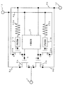
図1は、本発明の実施形態に係るESD保護回路の回路図である。 FIG. 1 is a circuit diagram of an ESD protection circuit according to an embodiment of the present invention.
本発明の実施形態に係るESD保護回路では、複数のFETで構成された内部回路5を有し、その出力側には、出力トランジスタ(Pチャンネル型トランジスタ)6a及び出力トランジスタ(Nチャンネル型トランジスタ)6bのゲート電極Gがそれぞれ接続されている。内部回路5は、内部回路用GNDライン9bを介してGND端子12に接続されると共に、内部回路用電源ライン8bを介して電源電圧VDD印可用の電源端子13に接続されている。出力トランジスタ6bのドレイン電極Dは、外部出力端子7に接続され、そのソース電極Sが周辺GNDライン9aに接続され、該周辺GNDライン9aはGND端子12に接続されている。出力トランジスタ6aのドレイン電極Dは、外部出力端子7に接続され、そのソース電極Sが周辺電源ライン8aに接続され、該周辺電源ライン8aは電源端子13に接続されている。
The ESD protection circuit according to the embodiment of the present invention includes an
このESD保護回路が従来の回路と異なる点は、出力トランジスタ(Nチャンネル型トランジスタ)6a、出力トランジスタ(Pチャンネル型トランジスタ)6bの各ゲート電極Gと周辺GNDライン及び周辺電源ラインとの間に保護トランジスタ30a、30b(Pチャンネル型トランジスタ、Nチャンネル型トランジスタ)、遅延回路、及び抵抗(32a、32b)が接続されていることである。 This ESD protection circuit is different from the conventional circuit in that protection is provided between each gate electrode G of the output transistor (N-channel type transistor) 6a and output transistor (P-channel type transistor) 6b, the peripheral GND line, and the peripheral power supply line. Transistors 30a and 30b (P-channel type transistors and N-channel type transistors), a delay circuit, and resistors (32a and 32b) are connected.
まず、VCC−を印加したときの動作について説明する。VCC−が印加されると、出力トランジスタ6aには、負方向の電圧が印加される。したがって、出力トランジスタ6aには、ブレークダウンするまで電流が流れない。一方、出力トランジスタ6bには、正方向の電圧が印加され、ドレイン電流は、ドレイン電極Dからソース電極Sを経てGND12へと流れる。 First, the operation when VCC- is applied will be described. When VCC− is applied, a negative voltage is applied to the output transistor 6a. Therefore, no current flows through the output transistor 6a until breakdown occurs. On the other hand, a positive voltage is applied to the output transistor 6b, and the drain current flows from the drain electrode D through the source electrode S to the GND 12.
保護トランジスタ(Nチャンネル型トランジスタ)30aは、ソース電極SがGND端子12に、ゲート電極Gが遅延回路31a及び抵抗32aを介してGND端子12に、ドレイン電極Dが出力トランジスタ6aのゲート電極Gに接続している。ここで、出力トランジスタ6bからGND端子12に流れた電流は、保護トランジスタ30aのゲート電極G及びソース電極Sに流れる。しかし、GND端子12と保護トランジスタ30aのゲート電極Gとの間には、抵抗32a及び遅延回路31a(例えばCR遅延回路など)が存在している。そのため、ゲート電極Gへは、ソース電極Sよりも遅れて、低い電流が流れる。 In the protection transistor (N-channel transistor) 30a, the source electrode S is connected to the GND terminal 12, the gate electrode G is connected to the GND terminal 12 through the delay circuit 31a and the resistor 32a, and the drain electrode D is connected to the gate electrode G of the output transistor 6a. Connected. Here, the current that flows from the output transistor 6b to the GND terminal 12 flows to the gate electrode G and the source electrode S of the protection transistor 30a. However, a resistor 32a and a delay circuit 31a (for example, a CR delay circuit) exist between the GND terminal 12 and the gate electrode G of the protection transistor 30a. Therefore, a low current flows to the gate electrode G later than the source electrode S.
このため保護トランジスタ30aは、一時的に電流を流し、出力トランジスタ6aのゲート電極GにVCC−が印加される。これにより出力トランジスタ6aは、ブレークダウンする前に電流を流し始める。 Therefore, the protection transistor 30a causes a current to flow temporarily, and VCC− is applied to the gate electrode G of the output transistor 6a. As a result, the output transistor 6a starts to flow current before breakdown.
上述の保護トランジスタ30a(Nチャンネル型トランジスタ)を追加することにより、出力トランジスタ6aのゲート絶縁膜の破壊を防止できる。 By adding the protection transistor 30a (N-channel transistor) described above, it is possible to prevent the gate insulating film of the output transistor 6a from being broken.
GND+を印加したときの動作について説明する。GND+が印加されると、出力トランジスタ6bには、負方向の電圧が印加される。したがって、出力トランジスタ6bには、ブレークダウンするまで電流が流れない。一方、出力トランジスタ6aには、正方向の電圧が印加され、ドレイン電流は、ドレイン電極Dからソース電極Sを経てVCC端子13へと流れる。 The operation when GND + is applied will be described. When GND + is applied, a negative voltage is applied to the output transistor 6b. Therefore, no current flows through the output transistor 6b until breakdown occurs. On the other hand, a positive voltage is applied to the output transistor 6a, and the drain current flows from the drain electrode D through the source electrode S to the VCC terminal 13.
保護トランジスタ(Pチャンネル型トランジスタ)30bは、ソース電極SがVCC端子13に、ゲート電極Gが遅延回路31b及び抵抗32bを介してVCC端子13に、ドレイン電極Dが出力トランジスタ6bのゲート電極Gに接続している。ここで、出力トランジスタ6aからVCC端子13に流れた電流は、保護トランジスタ30bのゲート電極G及びソース電極Sに流れる。しかし、VCC端子13と保護トランジスタ30bのゲート電極Gとの間には、抵抗32b及び遅延回路31b(例えばCR遅延回路など)が存在している。そのため、ゲート電極Gへは、ソース電極Sよりも遅れて、低い電流が流れる。 In the protection transistor (P-channel transistor) 30b, the source electrode S is connected to the VCC terminal 13, the gate electrode G is connected to the VCC terminal 13 via the delay circuit 31b and the resistor 32b, and the drain electrode D is connected to the gate electrode G of the output transistor 6b. Connected. Here, the current that flows from the output transistor 6a to the VCC terminal 13 flows to the gate electrode G and the source electrode S of the protection transistor 30b. However, a resistor 32b and a delay circuit 31b (for example, a CR delay circuit) exist between the VCC terminal 13 and the gate electrode G of the protection transistor 30b. Therefore, a low current flows to the gate electrode G later than the source electrode S.
このため保護トランジスタ30bは、一時的に電流を流し、出力トランジスタ6bのゲート電極GにGND+が印加される。これにより出力トランジスタ6bは、ゲート電極に電圧を印加し、ブレークダウンする前に電流を流し始める。 For this reason, the protection transistor 30b temporarily passes a current, and GND + is applied to the gate electrode G of the output transistor 6b. As a result, the output transistor 6b applies a voltage to the gate electrode and starts flowing a current before breakdown.
なお、保護トランジスタ30a及び30bは、出力トランジスタ6a及び6bに電流が流れているときは、常に電流は流れていないため、ESD保護回路の機能に悪影響を与えることはない。 The protection transistors 30a and 30b do not always adversely affect the function of the ESD protection circuit because current does not always flow when current flows through the output transistors 6a and 6b.
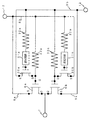
図2は、出力トランジスタ(6a、6b)のゲート電極Gを制御する内部回路5が存在しない時の回路構成である。内部回路5が存在しない場合、出力トランジスタ(6a、6b)のゲート電極Gは、VCC端末13又はGND端末12に直付せず、図中の抵抗(33a、33b)の様に抵抗を介して接続する。この時、出力トランジスタ6aに接続されている抵抗を保護トランジスタ6bに接続されている抵抗(32a、32b)よりも大きくする。これにより、保護トランジスタ(30a、30b)から出力トランジスタ(6a、6b)のゲート電極Gに印加される電圧に差が生じ、保護トランジスタ(30a、30b)をより効率的に駆動させることができる。
FIG. 2 shows a circuit configuration when there is no
5 内部回路
6a、6b 出力トランジスタ
7 外部出力端子
8a、8b 周辺電源ライン
9a、9b 周辺GNDライン
12 GND端子
13 VCC端子
30a、30b 保護トランジスタ
31a、31b 遅延回路
5 Internal circuit 6a, 6b Output transistor 7 External output terminal 8a, 8b Peripheral power supply line 9a, 9b Peripheral GND line 12 GND terminal 13 VCC terminal 30a, 30b Protection transistor 31a, 31b Delay circuit
Claims (7)
前記出力トランジスタのゲート電極と、前記周辺電源ライン又は前記周辺グランドラインとの間に前記出力トランジスタがブレークダウンする前にその両電極間の電位差を減少させる保護回路と、
前記保護回路は、
前記出力トランジスタのゲート電極と前記周辺電源ライン又は前記周辺グランドラインとの間に接続された前記保護トランジスタと、
前記保護トランジスタのゲート電極と前記周辺電源ライン又は前記周辺グランドラインとの間に遅延回路及び抵抗とを有することを特徴とするESD保護回路。 An internal circuit composed of a plurality of FETs, an internal circuit power supply line for supplying a power supply voltage to the internal circuit and an internal circuit ground line, and gate-controlled by the output of the internal circuit in accordance with the output of the internal circuit An output transistor that outputs a signal to an external output terminal or an external input / output terminal; and a peripheral power supply line and a peripheral ground line that are connected to the output transistor and apply a power supply voltage to the output transistor; In the ESD protection circuit in which the internal circuit ground line and / or the peripheral power supply line and / or the peripheral ground line are divided on the chip wiring,
A protection circuit for reducing a potential difference between the two electrodes before the output transistor breaks down between the gate electrode of the output transistor and the peripheral power supply line or the peripheral ground line;
The protection circuit is
The protection transistor connected between the gate electrode of the output transistor and the peripheral power supply line or the peripheral ground line;
An ESD protection circuit comprising a delay circuit and a resistor between a gate electrode of the protection transistor and the peripheral power supply line or the peripheral ground line.
前記出力トランジスタのゲート電極と、前記周辺電源ライン又は前記周辺グランドラインとの間に前記出力トランジスタがブレークダウンする前にその両電極間の電位差を減少させる保護回路と、
前記保護回路は、
前記出力トランジスタのゲート電極と前記周辺電源ライン又は前記周辺グランドラインとの間に接続された前記保護トランジスタと、
前記保護トランジスタのゲート電極と前記周辺電源ライン又は前記周辺グランドラインとの間に遅延回路及び第2の抵抗とを有することを特徴とするESD保護回路。 A plurality of first resistors, a resistor power supply line and a resistor ground line for supplying a power supply voltage to the resistors, and a signal that is gate-controlled by the outputs of the resistors and that corresponds to the outputs of the resistors are input to an external output terminal or an external input. An output transistor that outputs to an output terminal; and a peripheral power supply line and a peripheral ground line that are connected to the output transistor and apply a power supply voltage to the output transistor, the resistor power supply line, the resistor ground line, and the peripheral power supply line In the ESD protection circuit in which both and / or the peripheral ground line are divided on the chip wiring,
A protection circuit for reducing a potential difference between the two electrodes before the output transistor breaks down between the gate electrode of the output transistor and the peripheral power supply line or the peripheral ground line;
The protection circuit is
The protection transistor connected between the gate electrode of the output transistor and the peripheral power supply line or the peripheral ground line;
An ESD protection circuit comprising a delay circuit and a second resistor between a gate electrode of the protection transistor and the peripheral power supply line or the peripheral ground line.
Priority Applications (1)
| Application Number | Priority Date | Filing Date | Title |
|---|---|---|---|
| JP2004300819A JP4615957B2 (en) | 2004-10-14 | 2004-10-14 | ESD protection circuit |
Applications Claiming Priority (1)
| Application Number | Priority Date | Filing Date | Title |
|---|---|---|---|
| JP2004300819A JP4615957B2 (en) | 2004-10-14 | 2004-10-14 | ESD protection circuit |
Publications (2)
| Publication Number | Publication Date |
|---|---|
| JP2006114709A true JP2006114709A (en) | 2006-04-27 |
| JP4615957B2 JP4615957B2 (en) | 2011-01-19 |
Family
ID=36382975
Family Applications (1)
| Application Number | Title | Priority Date | Filing Date |
|---|---|---|---|
| JP2004300819A Expired - Fee Related JP4615957B2 (en) | 2004-10-14 | 2004-10-14 | ESD protection circuit |
Country Status (1)
| Country | Link |
|---|---|
| JP (1) | JP4615957B2 (en) |
Citations (5)
| Publication number | Priority date | Publication date | Assignee | Title |
|---|---|---|---|---|
| JPH05291511A (en) * | 1992-04-14 | 1993-11-05 | Oki Electric Ind Co Ltd | Semiconductor integrated circuit |
| JPH06177331A (en) * | 1992-06-05 | 1994-06-24 | American Teleph & Telegr Co <Att> | ESD protection of output buffer |
| JP2003031672A (en) * | 2001-07-19 | 2003-01-31 | Matsushita Electric Ind Co Ltd | Semiconductor integrated circuit device |
| JP2004055583A (en) * | 2002-07-16 | 2004-02-19 | Matsushita Electric Ind Co Ltd | Semiconductor integrated circuit device |
| JP2004221909A (en) * | 2003-01-15 | 2004-08-05 | Matsushita Electric Ind Co Ltd | Semiconductor device |
-
2004
- 2004-10-14 JP JP2004300819A patent/JP4615957B2/en not_active Expired - Fee Related
Patent Citations (5)
| Publication number | Priority date | Publication date | Assignee | Title |
|---|---|---|---|---|
| JPH05291511A (en) * | 1992-04-14 | 1993-11-05 | Oki Electric Ind Co Ltd | Semiconductor integrated circuit |
| JPH06177331A (en) * | 1992-06-05 | 1994-06-24 | American Teleph & Telegr Co <Att> | ESD protection of output buffer |
| JP2003031672A (en) * | 2001-07-19 | 2003-01-31 | Matsushita Electric Ind Co Ltd | Semiconductor integrated circuit device |
| JP2004055583A (en) * | 2002-07-16 | 2004-02-19 | Matsushita Electric Ind Co Ltd | Semiconductor integrated circuit device |
| JP2004221909A (en) * | 2003-01-15 | 2004-08-05 | Matsushita Electric Ind Co Ltd | Semiconductor device |
Also Published As
| Publication number | Publication date |
|---|---|
| JP4615957B2 (en) | 2011-01-19 |
Similar Documents
| Publication | Publication Date | Title |
|---|---|---|
| KR101034614B1 (en) | Static electricity protection circuit | |
| JP2007234718A (en) | Semiconductor integrated circuit device | |
| JP5165356B2 (en) | Semiconductor integrated circuit device | |
| JP3949647B2 (en) | Semiconductor integrated circuit device | |
| JP2010041013A (en) | Protection circuit | |
| JP4618164B2 (en) | Switch circuit | |
| US20040026741A1 (en) | Semiconductor integrated circuit device | |
| US6101077A (en) | Electrostatic protection circuit of a semiconductor device | |
| JP5241109B2 (en) | Semiconductor integrated circuit device | |
| US7911751B2 (en) | Electrostatic discharge device with metal option ensuring a pin capacitance | |
| JP3617425B2 (en) | Input interface circuit of semiconductor integrated circuit device | |
| JP4615957B2 (en) | ESD protection circuit | |
| JP2005142494A (en) | Semiconductor integrated circuit | |
| CN112310067A (en) | Electrostatic protection circuit | |
| JP5403592B2 (en) | Current drive circuit | |
| JP2007214420A (en) | Semiconductor integrated circuit | |
| JP4404589B2 (en) | Fuse circuit | |
| JP4562674B2 (en) | ESD protection circuit | |
| KR100907894B1 (en) | Electrostatic Discharge Protection Circuit | |
| JP2011119415A (en) | Semiconductor integrated device | |
| US7489486B2 (en) | Semiconductor device | |
| JP2008235625A (en) | Semiconductor integrated circuit | |
| JP3810401B2 (en) | Semiconductor device | |
| JP2016058423A (en) | ESD protection circuit | |
| JPS5814562A (en) | Semiconductor device |
Legal Events
| Date | Code | Title | Description |
|---|---|---|---|
| A621 | Written request for application examination |
Free format text: JAPANESE INTERMEDIATE CODE: A621 Effective date: 20071001 |
|
| A977 | Report on retrieval |
Free format text: JAPANESE INTERMEDIATE CODE: A971007 Effective date: 20100317 |
|
| A131 | Notification of reasons for refusal |
Free format text: JAPANESE INTERMEDIATE CODE: A131 Effective date: 20100323 |
|
| A521 | Written amendment |
Free format text: JAPANESE INTERMEDIATE CODE: A523 Effective date: 20100521 |
|
| A131 | Notification of reasons for refusal |
Free format text: JAPANESE INTERMEDIATE CODE: A131 Effective date: 20100629 |
|
| A521 | Written amendment |
Free format text: JAPANESE INTERMEDIATE CODE: A523 Effective date: 20100830 |
|
| TRDD | Decision of grant or rejection written | ||
| A01 | Written decision to grant a patent or to grant a registration (utility model) |
Free format text: JAPANESE INTERMEDIATE CODE: A01 Effective date: 20101012 |
|
| A01 | Written decision to grant a patent or to grant a registration (utility model) |
Free format text: JAPANESE INTERMEDIATE CODE: A01 |
|
| A61 | First payment of annual fees (during grant procedure) |
Free format text: JAPANESE INTERMEDIATE CODE: A61 Effective date: 20101021 |
|
| R150 | Certificate of patent or registration of utility model |
Free format text: JAPANESE INTERMEDIATE CODE: R150 |
|
| FPAY | Renewal fee payment (event date is renewal date of database) |
Free format text: PAYMENT UNTIL: 20131029 Year of fee payment: 3 |
|
| LAPS | Cancellation because of no payment of annual fees |