JP2006099057A - Method and device for packaging substrate - Google Patents
Method and device for packaging substrate Download PDFInfo
- Publication number
- JP2006099057A JP2006099057A JP2005218816A JP2005218816A JP2006099057A JP 2006099057 A JP2006099057 A JP 2006099057A JP 2005218816 A JP2005218816 A JP 2005218816A JP 2005218816 A JP2005218816 A JP 2005218816A JP 2006099057 A JP2006099057 A JP 2006099057A
- Authority
- JP
- Japan
- Prior art keywords
- thin film
- display device
- backplane
- interferometric modulator
- transparent substrate
- Prior art date
- Legal status (The legal status is an assumption and is not a legal conclusion. Google has not performed a legal analysis and makes no representation as to the accuracy of the status listed.)
- Withdrawn
Links
Images


Classifications
-
- B—PERFORMING OPERATIONS; TRANSPORTING
- B81—MICROSTRUCTURAL TECHNOLOGY
- B81C—PROCESSES OR APPARATUS SPECIALLY ADAPTED FOR THE MANUFACTURE OR TREATMENT OF MICROSTRUCTURAL DEVICES OR SYSTEMS
- B81C1/00—Manufacture or treatment of devices or systems in or on a substrate
- B81C1/00015—Manufacture or treatment of devices or systems in or on a substrate for manufacturing microsystems
- B81C1/00261—Processes for packaging MEMS devices
- B81C1/00333—Aspects relating to packaging of MEMS devices, not covered by groups B81C1/00269 - B81C1/00325
-
- B—PERFORMING OPERATIONS; TRANSPORTING
- B81—MICROSTRUCTURAL TECHNOLOGY
- B81C—PROCESSES OR APPARATUS SPECIALLY ADAPTED FOR THE MANUFACTURE OR TREATMENT OF MICROSTRUCTURAL DEVICES OR SYSTEMS
- B81C1/00—Manufacture or treatment of devices or systems in or on a substrate
- B81C1/00015—Manufacture or treatment of devices or systems in or on a substrate for manufacturing microsystems
- B81C1/00261—Processes for packaging MEMS devices
- B81C1/00277—Processes for packaging MEMS devices for maintaining a controlled atmosphere inside of the cavity containing the MEMS
- B81C1/00285—Processes for packaging MEMS devices for maintaining a controlled atmosphere inside of the cavity containing the MEMS using materials for controlling the level of pressure, contaminants or moisture inside of the package, e.g. getters
-
- G—PHYSICS
- G02—OPTICS
- G02B—OPTICAL ELEMENTS, SYSTEMS OR APPARATUS
- G02B26/00—Optical devices or arrangements for the control of light using movable or deformable optical elements
- G02B26/001—Optical devices or arrangements for the control of light using movable or deformable optical elements based on interference in an adjustable optical cavity
-
- G—PHYSICS
- G02—OPTICS
- G02B—OPTICAL ELEMENTS, SYSTEMS OR APPARATUS
- G02B26/00—Optical devices or arrangements for the control of light using movable or deformable optical elements
- G02B26/007—Optical devices or arrangements for the control of light using movable or deformable optical elements the movable or deformable optical element controlling the colour, i.e. a spectral characteristic, of the light
-
- G—PHYSICS
- G02—OPTICS
- G02B—OPTICAL ELEMENTS, SYSTEMS OR APPARATUS
- G02B26/00—Optical devices or arrangements for the control of light using movable or deformable optical elements
- G02B26/08—Optical devices or arrangements for the control of light using movable or deformable optical elements for controlling the direction of light
- G02B26/0816—Optical devices or arrangements for the control of light using movable or deformable optical elements for controlling the direction of light by means of one or more reflecting elements
- G02B26/0825—Optical devices or arrangements for the control of light using movable or deformable optical elements for controlling the direction of light by means of one or more reflecting elements the reflecting element being a flexible sheet or membrane, e.g. for varying the focus
-
- G—PHYSICS
- G02—OPTICS
- G02B—OPTICAL ELEMENTS, SYSTEMS OR APPARATUS
- G02B26/00—Optical devices or arrangements for the control of light using movable or deformable optical elements
- G02B26/08—Optical devices or arrangements for the control of light using movable or deformable optical elements for controlling the direction of light
- G02B26/0816—Optical devices or arrangements for the control of light using movable or deformable optical elements for controlling the direction of light by means of one or more reflecting elements
- G02B26/0833—Optical devices or arrangements for the control of light using movable or deformable optical elements for controlling the direction of light by means of one or more reflecting elements the reflecting element being a micromechanical device, e.g. a MEMS mirror, DMD
-
- B—PERFORMING OPERATIONS; TRANSPORTING
- B81—MICROSTRUCTURAL TECHNOLOGY
- B81B—MICROSTRUCTURAL DEVICES OR SYSTEMS, e.g. MICROMECHANICAL DEVICES
- B81B2201/00—Specific applications of microelectromechanical systems
- B81B2201/04—Optical MEMS
- B81B2201/047—Optical MEMS not provided for in B81B2201/042 - B81B2201/045
-
- B—PERFORMING OPERATIONS; TRANSPORTING
- B81—MICROSTRUCTURAL TECHNOLOGY
- B81C—PROCESSES OR APPARATUS SPECIALLY ADAPTED FOR THE MANUFACTURE OR TREATMENT OF MICROSTRUCTURAL DEVICES OR SYSTEMS
- B81C2203/00—Forming microstructural systems
- B81C2203/01—Packaging MEMS
- B81C2203/0136—Growing or depositing of a covering layer
-
- B—PERFORMING OPERATIONS; TRANSPORTING
- B81—MICROSTRUCTURAL TECHNOLOGY
- B81C—PROCESSES OR APPARATUS SPECIALLY ADAPTED FOR THE MANUFACTURE OR TREATMENT OF MICROSTRUCTURAL DEVICES OR SYSTEMS
- B81C2203/00—Forming microstructural systems
- B81C2203/01—Packaging MEMS
- B81C2203/0145—Hermetically sealing an opening in the lid
Abstract
Description
本発明の分野は、微小電気機械システム(microelectromechanical systems)(MEMS)及びそのようなシステムのパッケージングに係る。特に、本発明の分野は、干渉変調器及び薄膜バックプレーンを用いてそのような変調器を製作する方法に関する。 The field of the invention relates to microelectromechanical systems (MEMS) and the packaging of such systems. In particular, the field of the invention relates to methods of fabricating such modulators using interferometric modulators and thin film backplanes.
微小電気機械システム(MEMS)は、微小機械素子、アクチュエータ、及び電子機器を含む。微小機械素子は、堆積、エッチング、及び、あるいは、基板及び/又は堆積された材料の一部分をエッチングして取り除く、若しくは電子装置及び電子機械装置を形成するために複数の層を付加する、その他のマイクロマシニング・プロセスを使用して創り出されることができる。MEMS装置の1つのタイプは、干渉変調器と呼ばれる。干渉変調器は、1対の導電性プレートを具備し、その一方又は両方が、全体あるいは一部分が透明である及び/又は反射でき、そして適切な電子信号の印加により相対的動きが可能である。一方のプレートは、基板上に堆積された静止層を具備し、他方のプレートは、エアー・ギャップにより静止層から分離された金属膜を具備することができる。そのような装置は、広範囲のアプリケーションを有し、これらのタイプの装置の特性を利用すること及び/又は変形することは、この技術において有益であり、その結果、自身の特徴は、既存の製品を改善することに活用されることができ、未だ開発されていない新たな製品を創り出すことに活用されることができる。 Microelectromechanical systems (MEMS) include micromechanical elements, actuators, and electronics. Micromechanical elements can be deposited, etched, and / or etched away to remove portions of the substrate and / or deposited material, or add multiple layers to form electronic and electromechanical devices, etc. It can be created using a micromachining process. One type of MEMS device is called an interferometric modulator. An interferometric modulator comprises a pair of conductive plates, one or both of which can be wholly or partially transparent and / or reflective, and capable of relative movement by application of appropriate electronic signals. One plate may comprise a stationary layer deposited on the substrate and the other plate may comprise a metal film separated from the stationary layer by an air gap. Such devices have a wide range of applications, and it is beneficial in this technology to exploit and / or modify the characteristics of these types of devices, so that their features are It can be used to improve products, and can be used to create new products that have not yet been developed.
[発明の要約]
本発明のシステム、方法、及び装置は、それぞれ複数の態様を有し、そのいずれもが、その好ましい特性に単独で寄与するのではない。本発明の範囲を制限することなく、自身のより卓越した特徴が、ここに簡単に説明される。本明細書を熟考した後で、特に“特定の実施形態の詳細な説明”の項を読んだ後で、本発明の特徴が、その他のディスプレイ装置に対する利点をどのようにして提供するかを、理解するであろう。
[Summary of Invention]
Each of the systems, methods, and apparatus of the present invention has multiple aspects, none of which contributes solely to its preferred characteristics. Without limiting the scope of the invention, its more prominent features will now be briefly described. After reviewing this specification, and in particular after reading the “Detailed Description of Specific Embodiments” section, how the features of the present invention provide advantages over other display devices, You will understand.
1実施形態は、別々のバックプレーン、乾燥剤、及び封止に関する必要性を排除した干渉変調ディスプレイ装置のためのパッケージ構造を提供する。ディスプレイ装置は、透明基板、透明基板を透過した光を変調するために構成された干渉変調器、及び変調器上に配置され、透明基板と薄膜バックプレーンとの間のパッケージの内部に変調器を封止する薄膜バックプレーンを含む。ギャップは、変調器と薄膜との間に存在し、犠牲層の除去によって創り出される。 One embodiment provides a package structure for an interferometric modulation display device that eliminates the need for separate backplanes, desiccants, and seals. The display device includes a transparent substrate, an interferometric modulator configured to modulate light transmitted through the transparent substrate, and a modulator disposed inside the package between the transparent substrate and the thin film backplane. Includes a thin film backplane to be sealed. A gap exists between the modulator and the thin film and is created by removal of the sacrificial layer.
他の1つの実施形態にしたがって、ディスプレイ装置を製造する方法が提供される。本方法にしたがえば、透明基板が、用意され、そして干渉変調器が透明基板上に形成される。薄膜バックプレーンは、その後干渉変調器及び透明基板を覆って堆積され、透明基板と薄膜バックプレーンとの間の変調器を封止する。犠牲層は、薄膜バックプレーンの堆積に先立って干渉変調器上に堆積される。犠牲層は、薄膜バックプレーンの堆積の後で除去されて、前記干渉変調器と薄膜バックプレーンとの間にギャップを創り出す。 In accordance with another embodiment, a method for manufacturing a display device is provided. According to the method, a transparent substrate is provided and an interferometric modulator is formed on the transparent substrate. A thin film backplane is then deposited over the interferometric modulator and the transparent substrate, sealing the modulator between the transparent substrate and the thin film backplane. A sacrificial layer is deposited on the interferometric modulator prior to deposition of the thin film backplane. The sacrificial layer is removed after deposition of the thin film backplane to create a gap between the interferometric modulator and the thin film backplane.
さらに他の1つの実施形態にしたがって、微小電気機械システム・ディスプレイ装置が、提供され、透明基板、透明基板上に形成された干渉変調器、及び透明基板と薄膜バックプレーンとの間に干渉変調器を封じ込めるために透明基板に封止された薄膜バックプレーン、を具備する。キャビティが、干渉変調器と薄膜バックプレーンとの間に存在する。キャビティは、干渉変調器と薄膜バックプレーンとの間の犠牲層を除去することよって創り出される。 In accordance with yet another embodiment, a microelectromechanical system display device is provided and includes a transparent substrate, an interferometric modulator formed on the transparent substrate, and an interferometric modulator between the transparent substrate and the thin film backplane. A thin film backplane sealed to a transparent substrate. A cavity exists between the interferometric modulator and the thin film backplane. The cavity is created by removing the sacrificial layer between the interferometric modulator and the thin film backplane.
他の1つの実施形態にしたがって、ディスプレイ装置が提供され、透明基板、干渉変調器、干渉変調器を覆って堆積された薄膜バックプレーン、及び変調器と薄膜バックプレーンとの間のキャビティ、を具備する。干渉変調器は、透明基板を透過した光を変調するために構成され、そして透明基板上に形成される。薄膜バックプレーンは、干渉変調器を覆って形成され、透明基板と薄膜バックプレーンとの間のパッケージ内部に変調器を封止する。キャビティは、犠牲材料を除去することによって形成される。 In accordance with another embodiment, a display device is provided, comprising a transparent substrate, an interferometric modulator, a thin film backplane deposited over the interferometric modulator, and a cavity between the modulator and the thin film backplane. To do. The interferometric modulator is configured to modulate light transmitted through the transparent substrate and is formed on the transparent substrate. A thin film backplane is formed over the interferometric modulator and seals the modulator within the package between the transparent substrate and the thin film backplane. The cavity is formed by removing the sacrificial material.
さらに他の1つの実施形態にしたがって、ディスプレイ装置が提供される。ディスプレイ装置は、そこを通して光を透過させるための透過手段、透過手段を通って透過した光を変調するために構成された変調手段、及び透過手段と封止手段との間のパッケージ内部の変調手段を封止するための封止手段を含む。変調手段は、干渉変調器を具備し、そして封止手段は、薄膜を具備する。 In accordance with yet another embodiment, a display device is provided. The display device comprises a transmission means for transmitting light therethrough, a modulation means configured to modulate light transmitted through the transmission means, and a modulation means inside the package between the transmission means and the sealing means The sealing means for sealing is included. The modulating means comprises an interferometric modulator and the sealing means comprises a thin film.
[特定の実施形態の詳細な説明]
本発明のこれらの及びその他の態様は、下記の説明から及び添付された図面(正確に縮尺されていない)から、容易に明確になるであろう。図面は、発明を説明するためであり、制限するためではない。
[Detailed Description of Specific Embodiments]
These and other aspects of the invention will be readily apparent from the following description and from the accompanying drawings (not to scale). The drawings are for purposes of illustrating the invention and not for limiting it.
下記の詳細な説明は、本発明のある特定の実施形態に向けられる。しかしながら、発明は、多数の異なる方法で具体化されることができる。この明細書では、参照符合が、図面に与えられ、全体を通して同様の部分が類似の数字を用いて表される。下記の説明から明らかになるように、発明は、動画(例えば、ビデオ)であるか固定画面(例えば、静止画)であるかに係らず、及びテキストであるか画像であるかに係らず、画像を表示するために構成された任意の装置で実行されることができる。より詳しくは、本発明が種々の電子装置で実行される若しくは電子装置に関連付けられることができることが、予想される。電子装置は、携帯電話機、無線装置、パーソナル・ディジタル・アシスタンツ(PDAs)、ハンド−ヘルド又は携帯型コンピュータ、GPS受信機/ナビゲータ、カメラ、MP3プレーヤ、カムコーダ、ゲーム・コンソール、腕時計、時計、計算機、テレビ・モニタ、フラット・パネル・ディスプレイ、コンピュータ・モニタ、自動車ディスプレイ(例えば、走行距離計ディスプレイ、等)、コクピット制御装置及び/又はディスプレイ、カメラ・ファインダのディスプレイ(例えば、自動車の後方監視カメラのディスプレイ)、電子写真、電子ビルボード又はサイン、プロジェクタ、建築上の構造、パッケージング、及び芸術的な構造(例えば、宝石1個の画像のディスプレイ)のようなものであるが、限定されない。ここに説明されたものに類似の構造のMEMS装置も、電子スイッチング装置のような、非−ディスプレイ・アプリケーションで使用されこともできる。 The following detailed description is directed to certain specific embodiments of the invention. However, the invention can be embodied in a number of different ways. In this specification, reference numerals are provided in the drawings, and like parts are designated with like numerals throughout. As will become apparent from the description below, the invention is independent of whether it is a video (eg, video) or a fixed screen (eg, a still image), and whether it is text or an image, It can be executed on any device configured to display images. More specifically, it is anticipated that the present invention may be implemented on or associated with various electronic devices. Electronic devices include mobile phones, wireless devices, personal digital assistants (PDAs), hand-held or portable computers, GPS receivers / navigators, cameras, MP3 players, camcorders, game consoles, watches, watches, calculators, TV monitor, flat panel display, computer monitor, automobile display (eg, odometer display, etc.), cockpit controller and / or display, camera finder display (eg, vehicle rear view camera display) ), Electronic photographs, electronic billboards or signs, projectors, architectural structures, packaging, and artistic structures (e.g., display of a single piece of jewelry image). A MEMS device with a structure similar to that described herein can also be used in non-display applications, such as electronic switching devices.
干渉MEMSディスプレイ素子を具備する1つの干渉変調器ディスプレイの実施形態が、図1に図示される。これらの装置において、ピクセルは、明又は暗状態のいずれかである。明(“オン”又は“開路(open)”)状態では、ディスプレイ素子は、入射可視光の大部分をユーザに反射する。暗(“オフ”又は“閉路(close)”)状態にある場合は、ディスプレイ素子は、入射可視光をユーザに反射しない。実施形態に依存して、“オン”及び“オフ”状態の光反射率特性は、逆になることがある。MEMSピクセルは、選択された色を主に反射するように構成されることができ、白黒に加えてカラー表示を可能にする。 One interferometric modulator display embodiment comprising an interferometric MEMS display element is illustrated in FIG. In these devices, the pixels are in either a bright or dark state. In the bright (“on” or “open”) state, the display element reflects a large portion of incident visible light to a user. When in the dark (“off” or “closed”) state, the display element does not reflect incident visible light to the user. Depending on the embodiment, the light reflectance characteristics of the “on” and “off” states may be reversed. MEMS pixels can be configured to primarily reflect a selected color, allowing for a color display in addition to black and white.
図1は、視覚によるディスプレイ装置の一連のピクセル中の2つの隣接するピクセルを図示する等測図であり、ここでは、各ピクセルは、MEMS干渉変調器を具備する。複数の実施形態では、干渉変調器ディスプレイは、これらの干渉変調器の行/列アレイを具備する。各干渉変調器は、互いに可変であり制御可能な距離に位置する1対の反射層を含み、少なくとも1つの可変の大きさを有する共鳴光学的キャビティを形成する。1つの実施形態において、反射層の1つは、2つの位置の間を移動することができる。第1の位置では、ここではリリース状態(released state)と呼ぶ、可動層は、固定された部分反射層から比較的離れた距離に位置する。第2の位置では、可動層は、部分反射層により近くに隣接して位置する。2つの層から反射する入射光は、可動反射層の位置に依存して、積極的に(constructively)又は消極的に(destructively)干渉して、各ピクセルに対して全体が反射状態又は非反射状態のいずれかを作る。 FIG. 1 is an isometric view illustrating two adjacent pixels in a series of pixels of a visual display device, where each pixel comprises a MEMS interferometric modulator. In embodiments, the interferometric modulator display comprises a row / column array of these interferometric modulators. Each interferometric modulator includes a pair of reflective layers that are variable and controllable from each other, forming a resonant optical cavity having at least one variable size. In one embodiment, one of the reflective layers can move between two positions. In the first position, the movable layer, referred to herein as the released state, is located at a distance that is relatively far from the fixed partially reflective layer. In the second position, the movable layer is located closer adjacent to the partially reflective layer. Incident light reflected from the two layers interferes constructively or destructively depending on the position of the movable reflective layer, and is totally reflective or non-reflective for each pixel. Make one of them.
図1のピクセル・アレイの図示された部分は、2つの隣接する干渉変調器12a及び12bを含む。左の干渉変調器12aでは、可動かつ高反射層14aは、固定された部分反射層16aから所定の距離のリリースされた位置に図示される。右の干渉変調器12bでは、可動高反射層14bは、固定された部分反射層16bに隣接するアクチュエートされた位置に図示される。 The depicted portion of the pixel array of FIG. 1 includes two adjacent interferometric modulators 12a and 12b. In the left interferometric modulator 12a, the movable and highly reflective layer 14a is shown in a released position at a predetermined distance from the fixed partially reflective layer 16a. In the right interferometric modulator 12b, the movable highly reflective layer 14b is illustrated in an actuated position adjacent to the fixed partially reflective layer 16b.
固定層16a,16bは、電気的に導電性であり、部分的に透明であり、部分的に反射する、そして、例えば、透明基板20上にクロムとインジウム−スズ−酸化物のそれぞれの1又はそれより多くの層を堆積することにより製作されることができる。複数の層は、平行なストライプにパターニングされ、下記にさらに説明されるようにディスプレイ装置中の行電極を形成できる。可動層14a,14bは、支柱18の頂上及び複数の支柱18の間に介在する犠牲材料上に堆積された(行電極16a,16bに直交する)1層の堆積された金属層又は複数の層の一連の平行なストライプとして形成されることができる。犠牲材料がエッチされて除去されるときに、変形可能な金属層は、決められたエアー・ギャップ19だけ固定金属層から分離される。アルミニウムのような非常に電導性があり反射する材料が、変形可能な層として使用されることができ、そして、これらのストライプは、ディスプレイ装置において列電極を形成できる。
The fixing layers 16a, 16b are electrically conductive, partially transparent, partially reflective, and, for example, one or each of chromium and indium-tin-oxide on the
印加電圧がないと、キャビティ19は、2つの層14a,16aの間に維持され、変形可能な層は、図1のピクセル12aに図示されたように機械的に弛緩(relax)した状態にある。しかしながら、電位差が選択された行及び列に印加されると、対応するピクセルにおいて行及び列電極の交差点に形成されたキャパシタは、充電され、静電力が電極を強制的に引きつける。電圧が十分に高ければ、可動層は、変形され、図1に右のピクセル12bにより図示されたように、固定層に対して押し付けられる(この図に図示されていない誘電材料が、固定層上に堆積されることがあり、短絡することを防止し、分離距離を制御する)。この動きは、印加される電位差の極性に拘わらず同じである。このようにして、反射対非反射ピクセル状態を制御できる行/列アクチュエーションは、従来のLCD及びその他のディスプレイ技術において使用される多くの方法に類似している。 In the absence of an applied voltage, the cavity 19 is maintained between the two layers 14a, 16a, and the deformable layer is in a mechanically relaxed state as illustrated in the pixel 12a of FIG. . However, when a potential difference is applied to the selected row and column, the capacitor formed at the intersection of the row and column electrodes in the corresponding pixel is charged and electrostatic forces force the electrodes to attract. If the voltage is high enough, the movable layer is deformed and pressed against the fixed layer as illustrated by the right pixel 12b in FIG. 1 (dielectric material not shown in this figure is To prevent short circuit and control separation distance). This movement is the same regardless of the polarity of the applied potential difference. In this way, row / column actuation that can control the reflective vs. non-reflective pixel state is similar to many methods used in conventional LCD and other display technologies.
図2から図5は、ディスプレイ応用において干渉変調器のアレイを使用するための1つの具体例としてのプロセス及びシステムを説明する。図2は、本発明の態様を組み込むことができる電子装置の1実施形態を説明するシステム・ブロック図である。具体例としての実施形態において、電子装置は、プロセッサ21を含む。そのプロセッサ21は、いずれかの汎用のシングル・チップ又は複数チップ・マイクロプロセッサ、例えば、ARM,ペンティアム(登録商標)、ペンティアムII(登録商標)、ペンティアムIII(登録商標)、ペンティアムIV(登録商標)、ペンティアム(登録商標)プロ、8051、MIPS(登録商標)、パワーPC(登録商標)、ALPHA(登録商標)、若しくはディジタル・シグナル・プロセッサ、マイクロコントローラ、又はプログラム可能なゲート・アレイのようないずれかの特殊用途マイクロプロセッサ、であることができる。本技術において通常であるように、プロセッサ21は、1若しくはそれより多くのソフトウェア・モジュールを実行するために構成されることができる。オペレーティング・システムを実行することに加えて、プロセッサは、ウェブ・ブラウザ、電話アプリケーション、電子メール・プログラム、若しくはいずれかのその他のソフトウェア・アプリケーションを含む、1若しくはそれより多くのソフトウェア・アプリケーションを実行するように構成されることができる。 2-5 illustrate one exemplary process and system for using an array of interferometric modulators in a display application. FIG. 2 is a system block diagram illustrating one embodiment of an electronic device that may incorporate aspects of the invention. In the exemplary embodiment, the electronic device includes a processor 21. The processor 21 may be any general purpose single-chip or multi-chip microprocessor, such as ARM, Pentium (registered trademark), Pentium II (registered trademark), Pentium III (registered trademark), Pentium IV (registered trademark). , Pentium (R) Pro, 8051, MIPS (R), PowerPC (R), ALPHA (R), or any digital signal processor, microcontroller, or programmable gate array Can be a special purpose microprocessor. As is common in the art, the processor 21 can be configured to execute one or more software modules. In addition to executing the operating system, the processor executes one or more software applications, including a web browser, telephone application, email program, or any other software application. Can be configured as follows.
1実施形態では、プロセッサ21は、しかも、アレイ・コントローラ22と通信するように構成される。1実施形態では、アレイ・コントローラ22は、ピクセル・アレイ30に信号を供給する行ドライバ回路24及び列ドライバ回路26を含む。図1に図示されたアレイの断面は、図2に線1−1により示される。MEMS干渉変調器に関して、行/列アクチュエーション・プロトコルは、図3に説明されたこれらの装置のヒステリシス特性を利用することができる。これは、例えば、可動層をリリースされた状態からアクチュエートされた状態へ変形させるために10ボルトの電位差を必要とすることがある。しかしながら、電圧がその値から減少される場合に、10ボルトより下に電圧が降下して戻るとしても、可動層はその状態を維持する。図3の具体例としての実施形態では、可動層は、電圧が2ボルトより下に降下するまで完全にはリリースされない。そのようにして、図3に説明された例では、約3から7Vの電圧の範囲があり、そこでは、その範囲内で装置がリリースされた状態又はアクチュエートされた状態のいずれかで安定である、印加電圧のウィンドウが存在する。これは、ここでは“ヒステリシス・ウィンドウ”又は“安定ウィンドウ”として呼ばれる。図3のヒステリシス特性を有するディスプレイ・アレイに関して、行/列アクチュエーション・プロトコルは、行ストロービング(strobing)の期間に、アクチュエートされるべきストローブされた行のピクセルは、約10ボルトの電圧差を受け、そしてリリースされるべきピクセルは、零ボルトに近い電圧差を受ける。ストローブの後で、ピクセルは、約5ボルトの定常状態電圧差受け、その結果、ピクセルは、行ストローブがピクセルを置いたどんな状態にでも留まる。書き込まれた後で、各ピクセルは、電位差がこの例では3−7ボルトの“安定ウィンドウ”の範囲内であると判断する。この特徴は、アクチュエートされた又はリリースされた事前に存在する状態のいずれかに同じ印加された電圧条件の下で、図1に説明されたピクセル設計を安定にさせる。アクチュエートされた状態又はリリースされた状態であるかに拘わらず、干渉変調器の各ピクセルが、基本的に固定反射層と移動反射層とにより形成されたキャパシタであるので、この安定状態は、ほとんど電力消費なしにヒステリシス・ウィンドウの範囲内の電圧に保持されることができる。印加された電位が一定であるならば、基本的に電流は、ピクセルに流れ込まない。
In one embodiment, the processor 21 is also configured to communicate with the array controller 22. In one embodiment, the array controller 22 includes a row driver circuit 24 and a
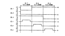
代表的なアプリケーションでは、ディスプレイ・フレームは、第1行中のアクチュエートされたピクセルの所望のセットにしたがって列電極のセットを示すこと(asserting)によって創り出される。行パルスは、それから行1の電極に印加されて、示された列ラインに対応するピクセルをアクチュエートする。列電極の示されたセットは、その後、第2行中のアクチュエートされたピクセルの所望のセットに対応するように変更される。パルスは、それから、行2の電極に印加されて、示された列電極にしたがって行2中の適切なピクセルをアクチュエートする。行1ピクセルは、行2パルスに影響されず、行1ピクセルは、行1パルスの間に設定された状態に留まる。これは、連続した方式で一連の行全体に対して繰り返され、フレームを生成する。一般に、フレームは、1秒当たり所望のフレームの数でこのプロセスを連続的に繰り返すことにより、新たなディスプレイ・データでリフレッシュされる及び/又は更新される。ディスプレイ・フレームを生成するためにピクセル・アレイの行及び列電極を駆動するための広範なプロトコルも、周知であり、本発明とともに使用されることができる。
In a typical application, a display frame is created by asserting a set of column electrodes according to the desired set of actuated pixels in the first row. A row pulse is then applied to the row 1 electrode, actuating the pixels corresponding to the indicated column lines. The indicated set of column electrodes is then changed to correspond to the desired set of actuated pixels in the second row. A pulse is then applied to the
図4及び図5は、図2の3×3アレイでディスプレイ・フレームを創り出すための1つの可能性のあるアクチュエーション・プロトコルを説明する。図4は、ピクセルが図3のヒステリシス曲線を表すために使用されることがある、列及び行電圧レベルの可能性のあるセットを説明する。図4の実施形態では、ピクセルをアクチュエートすることは、適切な列を−Vbiasに、そして適切な行を+ΔVに設定することを含む。これは、それぞれ−5V及び+5Vに対応することができる。ピクセルをリリースさせることは、適切な列を+Vbiasに、そして適切な行を同じ+ΔVに設定することにより達成され、ピクセル間で零ボルトの電位差を生成する。そこでは行電圧が零ボルトに保持されるこれらの行では、列が+Vbias又は−Vbiasであるかに拘らず、ピクセルが元々あった状態がどうであろうとも、ピクセルは、その状態で安定である。 FIGS. 4 and 5 illustrate one possible actuation protocol for creating a display frame with the 3 × 3 array of FIG. FIG. 4 illustrates a possible set of column and row voltage levels where a pixel may be used to represent the hysteresis curve of FIG. In the embodiment of FIG. 4, actuating a pixel includes setting the appropriate column to −V bias and the appropriate row to + ΔV. This can correspond to -5V and + 5V, respectively. Release of the pixel is accomplished by setting the appropriate column to + V bias and the appropriate row to the same + ΔV, producing a zero volt potential difference between the pixels. There, in those rows where the row voltage is held at zero volts, the pixel will remain in that state no matter what the pixel originally was, regardless of whether the column is + V bias or -V bias. It is stable.
図5Bは、そこではアクチュエートされたピクセルが反射しない図5Aに説明されたディスプレイ配列に結果としてなる、図2の3×3アレイに印加される一連の行及び列信号を示すタイミング図である。図5Aに説明されたフレームを書き込むことに先立って、ピクセルは、任意の状態であることができ、そしてこの例では、全ての行が0ボルトであり、全ての列が+5ボルトである。これらの印加電圧で、全てのピクセルは、自身の現在のアクチュエートされた状態又はリリースされた状態で安定である。 FIG. 5B is a timing diagram showing a series of row and column signals applied to the 3 × 3 array of FIG. 2 resulting in the display arrangement described in FIG. 5A where the actuated pixels do not reflect. . Prior to writing the frame described in FIG. 5A, the pixels can be in any state, and in this example, all rows are 0 volts and all columns are +5 volts. With these applied voltages, all pixels are stable in their current actuated or released state.
図5Aのフレームでは、ピクセル(1,1)、(1,2)、(2,2)、(3,2)及び(3,3)がアクチュエートされている。これを実現するために、行1に対する“ライン時間”の期間に、列1及び2は、−5ボルトに設定され、そして列3は、+5ボルトに設定される。全てのピクセルが3−7ボルトの安定ウィンドウの中に留まるため、これは、どのピクセルの状態も変化させない。行1は、その後、0から5ボルトまで上がり、零に戻るパルスでストローブされる。これは、(1,1)及び(1,2)ピクセルをアクチュエートし、(1,3)ピクセルをリリースする。アレイ中のその他のピクセルは、影響されない。望まれるように行2を設定するために、列2は、−5ボルトに設定され、そして列1及び3は、+5ボルトに設定される。行2に印加された同じストローブは、その後、ピクセル(2,2)をアクチュエートし、ピクセル(2,1)及び(2,3)をリリースする。再び、アレイのその他のピクセルは、影響されない。行3は、列2及び3を−5ボルトに、そして列1を+5ボルトに設定することより同様に設定される。行3ストローブは、図5Aに示されたように行3ピクセルを設定する。フレームを書き込んだ後、行電位は零に、そして列電位は+5又は−5ボルトのいずれかに留まることができ、ディスプレイは、その後、図5Aの配列で安定である。同じ手順が数十から数百の行及び列のアレイに対して採用されることができることが、歓迎される。しかも、行及び列アクチュエーションを実行するために使用された電圧のタイミング、シーケンス、及びレベルが、上記に概要を示された一般的な原理の範囲内で広範囲に変化されることができ、そして、上記の例は、具体的な例だけであり、任意のアクチュエーション電圧方法は、本発明とともに使用されることができる。
In the frame of FIG. 5A, pixels (1,1), (1,2), (2,2), (3,2) and (3,3) are actuated. To accomplish this, during the "line time" period for row 1,
上記に説明された原理にしたがって動作する干渉変調器の構造の詳細は、広範に変化できる。例えば、図6A−図6Cは、移動鏡構造の3つの異なる実施形態を図示する。図6Aは、図1の実施形態の断面であり、そこでは金属材料14のストライプが、直角に延びている支柱18上に堆積される。図6Bでは、可動反射材料14は、連結部(tether)32上に、角だけで支柱に取り付けられる。図6Cでは、可動反射材料14は、変形可能な層34から吊り下げられる。反射材料14に使用される構造的な設計及び材料が光学的特性に関して最適化されることができるため、及び変形可能な層34に使用される構造的な設計及び材料が所望の機械的特性に関して最適化できるため、この実施形態は、利点を有する。種々のタイプの干渉装置の製造は、例えば、米国公開出願2004/0051929を含む、種々の公開された文書に記載されている。多種多様な周知の技術が、一連の材料堆積、パターニング、及びエッチング工程を含む、上記に説明された構造を製造するために使用されることができる。 The details of the structure of interferometric modulators that operate in accordance with the principles set forth above may vary widely. For example, FIGS. 6A-6C illustrate three different embodiments of the moving mirror structure. FIG. 6A is a cross section of the embodiment of FIG. 1, where a stripe of metallic material 14 is deposited on struts 18 extending at right angles. In FIG. 6B, the movable reflective material 14 is attached to the column only at the corners on the tether 32. In FIG. 6C, the movable reflective material 14 is suspended from the deformable layer 34. Because the structural design and material used for the reflective material 14 can be optimized with respect to optical properties, and the structural design and material used for the deformable layer 34 is related to the desired mechanical properties. This embodiment has advantages because it can be optimized. The manufacture of various types of interferometric devices is described in various published documents, including, for example, US Published Application 2004/0051929. A wide variety of well-known techniques can be used to fabricate the structures described above, including a series of material deposition, patterning, and etching steps.
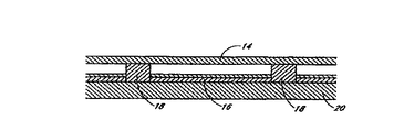
図7は、その中に干渉変調器830が従来のバックプレーン又はキャップなしに透明基板810上にパッケージされるパッケージ構造800を図示する。図7に図示されたパッケージ構造800は、バックプレーンだけでなく別々の封止、同様に乾燥剤に対する必要性を排除できる。
FIG. 7 illustrates a
図7に示された実施形態にしたがって、上記に説明されたように、干渉変調器830を封じ込めるために透明基板にバックプレーンを封止する代わりに、薄膜又は超構造820が、透明基板810を覆って堆積されて、パッケージ構造800の内部に干渉変調器830を封じ込める。薄膜820は、環境中の有害な成分から干渉変調器830を保護する。
In accordance with the embodiment shown in FIG. 7, instead of sealing the backplane to the transparent substrate to contain the
図7に示された実施形態にしたがった干渉変調器をパッケージする方法は、下記により詳細に説明される。ここで説明されるパッケージ及びパッケージング方法は、上記に説明された干渉変調器を含むが、これらに限定されることはない、いずれかの干渉変調器をパッケージするために使用されることができる。 A method of packaging an interferometric modulator according to the embodiment shown in FIG. 7 is described in more detail below. The packaging and packaging methods described herein can be used to package any interferometric modulator, including but not limited to the interferometric modulators described above. .
上記に説明されたように、干渉変調器830は、透明基板を通過した光を反射するように構成され、可動鏡14a,14bのような、移動部品を含む。したがって、そのような移動部品が動くことを可能にするために、ギャップ又はキャビティ840が、そのような移動部品と薄膜820との間に好ましくは創り出される。ギャップ又はキャビティ840は、可動鏡14a,14bのような、干渉変調器830の機械部品を動くようにする。薄膜820が、干渉変調器830を封じ込めるために堆積される前に、(図9に示された)犠牲層850が、干渉変調器830及び透明基板810を覆って好ましくは堆積され、その後、除去されて、干渉変調器830と薄膜820との間にキャビティ840を創り出す。これは、下記により詳細に説明される。
As described above, the
図8は、従来のバックプレーン又はキャップを用いないで干渉変調器をパッケージする方法の1つの実施形態を示す。透明基板810が、ステップ900において最初に用意され、そして干渉変調器830が、ステップ910において透明基板810上に形成される。干渉変調器830は、好ましくは、図1−6を参照して説明されたプロセスにしたがって形成される。透明基板810は、MEMS装置がその上に構築される、薄膜を有することが可能ないずれかの透明基板であることができる。そのような透明基板は、ガラス、プラスチック、及び透明ポリマを含むが、これらに限定されない。画像は、画面として働く透明基板810を通して表示される。
FIG. 8 illustrates one embodiment of a method for packaging an interferometric modulator without using a conventional backplane or cap. A
干渉変調器830が、透明基板810上に形成された後で、犠牲層850は、ステップ920において、好ましくは、干渉変調器830の上面及び透明基板810を覆って堆積される。犠牲層850は、その後、フォトリソグラフ技術を使用して、ステップ930においてパターニングされる。このパターニング・プロセスは、好ましくは、干渉変調器830に犠牲層850を局在化させ、干渉変調器830の周囲の透明基板810を露出させる。犠牲層850が堆積され、パターニングされた後で、ステップ940において、薄膜820が、その後、構造全体を覆って堆積される。薄膜820は、フォトリソグラフ技術を使用して、ステップ950においてパターニングされる。このパターニング・プロセスは、薄膜820を犠牲層850に局在化させる。このパターニング工程は、しかも、この後に続く犠牲層850の除去を可能にする薄膜820の凹凸(features)を与える。プロセス中のこの時点で、追加の犠牲層が、干渉変調器構造の内部に残ることがあり、又は残らないことがある。パターニング工程930は、犠牲層850の除去、同様に干渉変調器830内部に残っているいかなる犠牲層の除去を可能にする。ステップ960において、犠牲層850及び干渉変調器830内部のいずれかの犠牲層が、除去されて、干渉変調器830と薄膜820との間にキャビティ840を残し、干渉変調器830の加工を完了する。ステップ970において、薄膜820中の凹凸又は開口は、封止される。
After the
1実施形態にしたがって、干渉変調器830は、好ましくは透明基板810上に形成される。干渉変調器830の固定鏡16a,16bは、透明基板810に隣接し、可動鏡14a,14bは、固定鏡16a,16bを覆って形成されて、その結果、可動鏡14a,14bは、図7に示された実施形態のパッケージ構造のキャビティ840内部で移動できる。
According to one embodiment, the
干渉変調器830を形成するために、1つの実施形態における透明基板810は、インジウム・スズ酸化物(indium tin oxide)(ITO)を用いて覆われる。ITOは、好ましくは約500Åの厚さに、化学気相堆積法(chemical vapor deposition)(CVD)及びスパッタリングを含む、標準的な堆積技術により堆積されることができる。クロムの比較的薄い層が、好ましくはITOを覆って堆積される。ITO/クロム2重層は、それから列にエッチングされ、パターニングされて、列電極16a,16bを形成する。二酸化シリコン(SiO2)の層が、好ましくはITO/クロム列を覆って形成されて、部分的に反射する固定鏡16a,16bを創り出す。シリコン(Si)の犠牲層は、好ましくはその構造を覆って堆積されて(そして後でリリースされて)、固定鏡16a,16bと可動鏡14a,14bとの間に共鳴光学キャビティを創り出す。その他の実施形態では、この犠牲層は、モリブデン(Mo)、タングステン(W),又はチタン(Ti)で形成されることができる。
To form the
好ましくはアルミニウムで形成された他の1つの鏡層が、シリコンの犠牲層を覆って堆積されて、干渉変調器830の可動鏡14a,14bを形成する。この鏡層は、堆積され、列電極16a,16bに垂直な行にパターニングされて、上記に説明された行/列アレイを創り出す。その他の実施形態では、この鏡層は、例えば、銀(Ag)又は金(Au)のような高反射の材料を具備できる。あるいは、この鏡層は、適切な光学的及び機械的特性を与えるために構成された金属の積層であることができる。
Another mirror layer, preferably made of aluminum, is deposited over the sacrificial layer of silicon to form the movable mirrors 14a, 14b of the
可動鏡14a,14bが形成された後で、シリコンの犠牲層は、好ましくはガス・エチング・プロセスを使用して除去されて、固定鏡16a,16bと可動鏡14a,14bとの間に光学的キャビティを創り出す。ある実施形態では、この犠牲層は、薄膜820が形成された後で除去される。標準的なエッチング技術が、シリコンの犠牲層を除去するために使用されることができる。個々のリリース・エッチングは、リリースされるべき材料に依存する。例えば、2フッ化キセノン(XeF2)が、シリコン犠牲層を除去するために使用されることができる。1実施形態では、複数の鏡16a,16b,14a,14bの間のシリコンの犠牲層は、薄膜820が形成された後で除去される。干渉変調器830の各層が標準的な堆積技術及び標準的なフォトリソグラフ技術を使用して好ましくは堆積され、パターニングされることを、熟練工は、歓迎する。
After the movable mirrors 14a, 14b are formed, the sacrificial layer of silicon is preferably removed using a gas etching process to optically connect the fixed mirrors 16a, 16b and the movable mirrors 14a, 14b. Create a cavity. In some embodiments, this sacrificial layer is removed after
図9に示されたように、干渉変調器830が透明基板810の上に形成された後で、もう1つの犠牲層850が、干渉変調器830の上面及び透明基板810を覆って堆積される。犠牲層850は、例えば、モリブデン(Mo)、シリコン(Si)、タングステン(W)、又はチタン(Ti)のような材料で形成されることができる。これらの材料は、薄膜820の堆積の後でリリースされることができる。ある実施形態では、犠牲層850は、ポリマ、スピン−オン・ガラス、又は酸化物のような材料で形成される。犠牲層の材料に依存して異なることがある、除去プロセスが、下記により詳細に説明される。
As shown in FIG. 9, after the
上層の犠牲層850は、その材料が十分なステップ・カバレッジを与え、所望の厚さに堆積できる限りは、モリブデン(Mo)、シリコン(Si)、タングステン(W)、チタン(Ti)、ポリマ、スピン−オン・ガラス、又は酸化物のいずれかで形成されることができることを、熟練工は歓迎する。犠牲層850の厚さは、薄膜820と干渉変調器830とを分離するために十分であるべきである。1つの実施形態では、上層の犠牲層850は、約1000Åから1μmの範囲の、より好ましくは約1000Åから5000Åの範囲の厚さに堆積される。1つの実施形態では、犠牲層850は、標準的なフォトリソグラフ技術を使用してパターニングされ、エッチングされる。
The upper
1つの実施形態では、薄膜820は、図10に示されたように、犠牲層850の上面全体を覆って堆積されることができる。薄膜820は、既知の堆積技術を使用して犠牲層850を覆って形成されることができる。薄膜820がパターニングされ、エッチングされた後で、犠牲層850は、リリースされて、キャビティ840を形成する。キャビティ840の中では、可動鏡14a,14bは、図8に示されたように、移動できる。
In one embodiment, the
薄膜820は、好ましくはパターニングされエッチングされて、少なくとも1の開口部をその中に形成する。開口部を通して、2フッ化キセノン(XeF2)のような、リリース材料は、パッケージ構造800の内部に導入されることができ、犠牲層850をリリースする。これらの開口部の数及び大きさは、所望の犠牲層850のリリース・レートに依存する。開口部は、薄膜820中のどこにでも置かれることができる。ある実施形態では、犠牲層850及び(固定鏡16a,16bと可動鏡14a,14bとの間の)干渉変調器内部の犠牲層は、同時にリリースされることができる。その他の実施形態では、犠牲層850及び干渉変調器内部の犠牲層は、干渉変調器内部の犠牲層の除去に先立って犠牲層850が除去され、同時に除去されない。
The
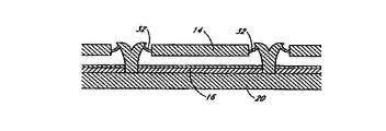
代わりのリリース技術は、図11の実施形態により示される。図11は、パッケージ構造800の実施形態の上面図であり、薄膜820が堆積されパターニングされた後で、犠牲層850がリリースされる前である。図11に示されたように、犠牲層850は、堆積され、複数の突起855を有するようにパターニングされる。薄膜820が、それから犠牲層850及び透明基板810を覆って堆積される。薄膜820が堆積された後で、図11に示されたように、薄膜820は、その後、好ましくは各横方向にエッチ・バックされる。パッケージ構造800は、それから、2フッ化キセノン(XeF2)のようなリリース材料に曝されることができる。リリース材料は、初めに露出された犠牲層850材料と反応し、そしてそれからパッケージ構造の側面上の犠牲層850の除去により突起855部に創り出された開口部を通してパッケージ構造800に浸入する。突起855の数及び大きさは、犠牲層850のリリースの要求されるレートに依存することが、理解される。
An alternative release technique is illustrated by the embodiment of FIG. FIG. 11 is a top view of an embodiment of the
モリブデン(Mo)、シリコン(Si)、タングステン(W)、又はチタン(Ti)の犠牲層を除去するために、2フッ化キセノン(XeF2)が、薄膜820の1個の開口部又は複数の開口部を通してパッケージ構造800の内部へ導入されることができる。2フッ化キセノン(XeF2)は、犠牲層850と反応して除去し、干渉変調器830と薄膜820との間にキャビティ840を残す。スピン−オン・ガラス又は酸化物からなる犠牲層850は、薄膜820が堆積された後で、好ましくはガスエッチされ又は気相エッチされて犠牲層850を除去する。除去プロセスが犠牲層850の材料に依存することを、熟練工は、歓迎する。
To remove the sacrificial layer of molybdenum (Mo), silicon (Si), tungsten (W), or titanium (Ti), xenon difluoride (XeF2) is used to form one or more openings in the
干渉変調器830の可動鏡14a,14bのような機械的な部品を自由に移動させるために、キャビティ840が、干渉変調器830の背後に必要であることも、熟練工は歓迎する。キャビティ840の結果としての高さhは、犠牲層850の厚さに依存する。
The skilled worker also welcomes that a
ある実施形態では、薄膜820は、ニッケル、アルミニウム、及びその他のタイプの金属及びホイルを含むが、これらに限定されない、密封性又は疎水性であるいずれかのタイプの材料であることができる。薄膜820は、しかも、二酸化シリコン、酸化アルミニウム、又は窒化物を含むが、これらに限定されない、絶縁物からなることができる。
In certain embodiments, the
あるいは、薄膜820は、非密封性の材料からなることがある。適切な非密封性の材料は、例えば、PMMA、エポキシ及び有機又は無機のスピン−オン・ガラス(SOG)タイプの材料のようなポリマを含む。非密封性の材料が薄膜820に使用されるのであれば、図12に示されたように、保護膜層860は、好ましくは非密封性の薄膜を覆って形成されて、図12に示されたように、犠牲層850が除去された後で干渉変調器830への追加の保護を与える。そのような保護膜層860は、好ましくは蒸気バリアからなり、約1000Åから約10000Åの厚さを有する。1つの実施形態では、保護膜層860は、バリックス(登録商標)、カルフォルニア州、サンノゼのヴィテックス・システムズ社から市場で利用できる薄膜コーティング、である。そのような保護膜は、ある層がガス密封の目的で働くことができ、ある層が、下記に説明されるように、機械的な目的で働くことができる多重の積層であり得る。
Alternatively, the
薄膜820が疎水性材料である、ある種の実施形態では、ハーメチック・シールを創り出す必要はないが、それにも拘らず従来のバックプレーンに対する必要性を排除できる。必要とされるいずれかのさらなる湿気バリアが、モジュール・レベルでパッケージングの次のステップに組み込まれることができることが、歓迎される。
In certain embodiments where the
薄膜820は、約1μmの厚さに化学気相堆積法(CVD)又はその他の適切な堆積方法により堆積されることができる。熟練工は、薄膜820の厚さが薄膜820に選択された材料の固有の材料特性に依存できることを理解する。
The
薄膜820は、透明又は不透明のいずれかである可能性がある。画像が薄膜820を通して表示されず、むしろ透明基板810を通して表示されるため、薄膜820が透明である必要性がないことが、理解される。透明材料が、干渉変調器830の保護のための薄膜820としての使用に関して適している材料特性を有することができるので、熟練工は、スピン−オン・ガラスのような透明材料が、薄膜820を形成するために使用されることができることを歓迎する。例えば、透明であるスピン−オン・ガラスのような材料は、パッケージ構造800内部の干渉変調器830により大きな強度及び保護を与えられる。
The
犠牲層850がリリースされた後で、薄膜820中の(複数の)開口部は、好ましくは封止される。ある実施形態では、エポキシがこれらの開口部を封止するために使用される。その他の材料が同様に使用されることができ、高い粘性を有する材料が好ましいことを、熟練工は、歓迎する。開口部が十分に小さければ(例えば、1μより小さい)、薄膜820材料の他の1つの層が、開口部を封止するために使用されることができる。
After the
密封性薄膜820を有するある種の実施形態を含むが、これらに限定されることはない、複数の実施形態では、保護膜層860は、図12に示されたように、犠牲層850が除去された後で薄膜820を覆って堆積されることができる。保護膜層は、好ましくはポリマから形成され、そして好ましくは約1μmから数メリメートルの厚さを有する。保護膜層860は、追加の強度及び硬さを薄膜820に与える。薄膜820中の(複数の)開口部が十分に小さい(例えば、1μより小さい)ある種の実施形態では、保護膜層860は、上記に説明されたように、薄膜820のもう1つの層よりはむしろ開口部を封止するために使用されることができる。
In some embodiments, including but not limited to certain embodiments having a sealable
薄膜820は、図7に示されたように、好ましくは雰囲気環境からパッケージ構造800の内部を密封して封止する。薄膜820がハーメチック・シールを提供できるので、水分が雰囲気環境からパッケージ構造800に進入することをハーメチック・シールが防止するために、それゆえ、乾燥剤に対する必要性は削除される。他の1つの実施形態では、薄膜820は、準ハーメチック・シールを提供し、乾燥剤が過剰な水分を吸収するためにパッケージ構造800の内部に含まれる。
As shown in FIG. 7, the
乾燥剤は、パッケージ構造800の内部に内在する水分を制御するために使用される。しかしながら、選択された材料に依存して、薄膜820がハーメチック・シールを提供できるので、乾燥剤は、雰囲気からパッケージ構造800の内部に水分が移動することを防止する必要がない。準密封性薄膜820の場合には、必要とされる乾燥剤の量が、削減される。
The desiccant is used to control moisture inherent in the
ある実施形態では、この実施形態にしたがった干渉変調器をパッケージングする方法は、フロント−エンドの処理にパッケージ構造800のシーリングを統合し、別々のバックプレーン、乾燥剤、及び封止に対する必要性を削除する。それによって、パッケージングのコストを低下させる。他の1つの実施形態では、薄膜820は、乾燥剤に対する必要性を削除することよりはむしろ、必要とされる乾燥剤の量を削減する。これらの実施形態にしたがったパッケージングは、乾燥剤及び封止の両方に関する材料の制約を削減する、これによって、コストを削減するために、より大きな選択若しくは材料、外形、及び機会を可能にする。薄膜820は、バックプレーンの削除を可能にするために密封性の要求を削減できるだけでなく、モジュール・レベルのパッケージングに組み込まれようとしているいずれかの追加の水分バリア要求を可能にする。パッケージ構造をできる限り薄く保つことは、一般に好ましく、図7に示されたパッケージ構造800は、薄い構造を提供する。
In certain embodiments, a method for packaging an interferometric modulator according to this embodiment integrates the sealing of the
乾燥剤に対する必要性の削除も、パッケージ構造800をより一層薄くすることを可能にする。一般的に、乾燥剤を含んでいるパッケージでは、装置のライフタイム予想は、乾燥剤のライフタイムに依存することがある。乾燥剤が完全に使い尽くされた場合に、十分な水分がパッケージ構造に浸入して、干渉変調器にダメージを生じさせるので、干渉変調器ディスプレイは、不良になる。装置の理論的な最大ライフタイムは、パッケージの中への水蒸気フラックスと同様に乾燥剤の量及びタイプにより決定される。このパッケージ構造800では、本実施形態のパッケージ構造800がいかなる乾燥剤も含んでいないので、干渉変調器830は、乾燥剤が消費されることに起因する不良にならない。
The elimination of the need for a desiccant also allows the
他の1つの実施形態では、薄膜820は、密封性ではなく、2フッ化キセノン(XeF2)又は他の除去できるガスを透過させることができる。このガスは、犠牲層850と反応して除去して、干渉変調器830と薄膜820との間にキャビティ840を残す。この実施形態にしたがって、薄膜820に適している複数の材料は、多孔質アルミニウム及びある種のエーロゲルを含むが、限定されることはない。この実施形態では、薄膜820が2フッ化キセノン(XeF2)又は他の1つの除去ガスを透過する限りは、いかなる開口部を薄膜820に形成する必要性がない。好ましくは、犠牲層850の除去の後で、密封性の保護膜層860が薄膜820を覆って堆積されて、パッケージ構造800を密封して封止する。これらの実施形態では、保護膜層860は、好ましくは金属により形成される。
In another embodiment, the
図13A及び13Bは、ディスプレイ装置2040の実施形態を説明するシステム・ブロック図である。ディスプレイ装置2040は、例えば、セルラ又は携帯電話機である可能性がある。しかしながら、ディスプレイ装置2040の同じ構成要素又はそのわずかな変形も、テレビ及び携帯型メディア・プレーヤのような種々のタイプのディスプレイ装置を説明する。
13A and 13B are system block diagrams illustrating an embodiment of a
ディスプレイ装置2040は、ハウジング2041、ディスプレイ2030、アンテナ2043、スピーカ2045、入力装置2048、及びマイクロフォン2046を含む。ハウジング2041は、一般に当業者に周知の各種の製造技術のいずれかから形成され、射出成型、及び真空形成を含む。その上、ハウジング2041は、プラスチック、金属、ガラス、ゴム、及びセラミックス、又はこれらの組み合わせを含むが、限定されないいずれかの種々の材料から形成されることができる。1つの実施形態では、ハウジング2041は、除去可能な部分(図示せず)を含み、異なる色、若しくは異なるロゴ、絵柄、又はシンボルを含むその他の取り外し可能な部分と取り替えられることができる。
The
具体例としてのディスプレイ装置2040のディスプレイ2030は、ここに説明されたように、双安定ディスプレイを含む種々のディスプレイのいずれかであることができる。その他の実施形態では、当業者に周知であるように、ディスプレイ2030は、上記に説明されたような、プラズマ、EL、OLED、STN LCD、又はTFT LCDのようなフラット−パネル・ディスプレイ、若しくはCRT又はその他の真空管装置のような、非フラット−パネル・ディスプレイを含む。しかしながら、本実施形態を説明する目的のために、ディスプレイ2030は、ここに説明されたように、干渉変調器ディスプレイを含む。
The
具体例としてのディスプレイ装置2040の1つの実施形態の構成要素が、図13Bに模式的に図示される。図示された具体例としてのディスプレイ装置2040は、ハウジング2041を含み、少なくとも部分的にその中に閉じ込められた付加的な構成要素を含むことができる。例えば、1つの実施形態では、具体例としてのディスプレイ装置2040は、トランシーバ2047に接続されたアンテナ2043を含むネットワーク・インターフェース2027を含む。トランシーバ2047は、プロセッサ2021に接続され、プロセッサ2021は調整ハードウェア2052に接続される。調整ハードウェア2052は、信号を調整する(例えば、信号をフィルタする)ために配置されることができる。調整ハードウェア2052は、スピーカ2045及びマイクロフォン2046に接続される。プロセッサ2021も、入力装置2048及びドライバ・コントローラ2029に接続される。ドライバ・コントローラ2029は、フレーム・バッファ2028に接続され、そしてアレイ・ドライバ2022に接続される。アレイ・ドライバ2022は、順番にディスプレイ・アレイ2030に接続される。電源2050は、固有の具体例としてのディスプレイ装置2040設計によって必要とされるように全ての構成要素に電力を供給する。
The components of one embodiment of
ネットワーク・インターフェース2027は、アンテナ2043及びトランシーバ2047を含み、その結果、具体例としてのディスプレイ装置2040は、ネットワークを介して1又はそれより多くの装置と通信できる。1つの実施形態では、ネットワーク・インターフェース2027は、しかも、プロセッサ2021の要求を軽減させるためにある種の処理能力を持つことができる。アンテナ2043は、信号を送信し受信するために当業者に公知にいずれかのアンテナである。1つの実施形態では、アンテナは、IEEE802.11(a),(b),又は(g)を含む、IEEE802.11規格にしたがってRF信号を送信し、受信する。他の1つの実施形態では、アンテナは、ブルートゥース(BLUETOOTH)規格にしたがってRF信号を送信し、受信する。セルラ電話機の場合には、アンテナは、CDMA、GSM、AMPS若しくは無線セル電話ネットワークの内部で通信するために使用されるその他の公知の信号を受信するように設計される。トランシーバ2047は、アンテナ2043から受信された信号を事前処理し、その結果、信号が受信され、プロセッサ2021によってさらに操作されることができる。トランシーバ2047は、しかも、プロセッサ2021から受信された信号を処理し、その結果、信号はアンテナ2043を介して具体例としてのディスプレイ装置2040から送信されることができる。
代わりの実施形態では、トランシーバ2047は、受信機によって置き換えられることがある。しかも他の1つの代わりの実施形態では、ネットワーク・インターフェース2027は、画像ソースによって置き換えられることができる。画像ソースは、プロセッサ2021に送られるべき画像データを記憶できる、又は発生できる。例えば、画像ソースは、ディジタル・ビデオ・ディスク(digital video disc)(DVD)又は画像データを含むハード−ディスク・ドライブ、若しくは画像データを発生するソフトウェア・モジュールであることができる。
In an alternative embodiment, the
プロセッサ2021は、一般に具体例としてのディスプレイ装置2040の総合的な動作を制御する。プロセッサ2021は、ネットワーク・インターフェース2027又は画像ソースからの圧縮された画像データのような、データを受信し、そしてデータを生の画像データに、若しくは生の画像データに容易に処理されるフォーマットに処理する。プロセッサ2021は、その後、処理されたデータをドライバ・コントローラ2029へ、又は記憶のためにフレーム・バッファ2028へ送る。生のデータは、一般的に、画像の内部でのそれぞれの位置における画像特性を識別する情報を呼ぶ。例えば、そのような画像特性は、色彩、彩度、及びグレー・スケール・レベルを含むことができる。
The
1つの実施形態では、プロセッサ2021は、マイクロコントローラ、CPU、若しくは論理ユニットを含み、具体例としてのディスプレイ装置2040の動作を制御する。調整ハードウェア2052は、一般に、スピーカ2045に信号を送信するために、そして、マイクロフォン2046から信号を受信するために、増幅器及びフィルタを含む。調整ハードウェア2052は、具体例としてのディスプレイ装置2040内部の独立した構成要素であることができる、若しくは、プロセッサ2021又はその他の構成要素の内部に組み込まれることができる。
In one embodiment,
ドライバ・コントローラ2029は、プロセッサ2021により発生された生の画像データをプロセッサ2021から直接又はフレーム・バッファ2028からのいずれかで取得し、そしてアレイ・ドライバ2022への高速送信に適切であるように生の画像データを再フォーマット化する。具体的には、ドライバ・コントローラ2029は、生の画像データをラスタ状のフォーマットを有するデータ・フローに再フォーマットする、その結果、データ・フローは、ディスプレイ・アレイ2030全体をスキャニングするために適した時間の順番を有する。それから、ドライバ・コントローラ2029は、フォーマット化された情報をアレイ・ドライバ2022へ送る。LCDコントローラのような、ドライバ・コントローラ2029が独立型の集積回路(Integrated Circuit)(IC)としてプロセッサ2021にしばしば関連付けられるけれども、そのようなコントローラは、複数の方法で与えられることができる。これらは、ハードウェアとしてプロセッサ2021に搭載される、ソフトウェアとしてプロセッサ2021に搭載される、若しくはアレイ・ドライバ2022を用いたハードウェアに完全に統合されることができる。
The
一般的に、アレイ・ドライバ2022は、フォーマット化された情報をドライバ・コントローラ2029から受信し、そしてビデオ・データをウェーブフォームの並列セットに再フォーマット化する。ウェーブフォームの並列セットは、ディスプレイのピクセルのx−y行列から来る毎秒数回から数百回そして時には数千回のリード(lead)を適用される。
In general, the
1つの実施形態では、ドライバ・コントローラ2029、アレイ・ドライバ2022、及びディスプレイ・アレイ2030は、ここに説明されたいずれのタイプのディスプレイに対して適切である。例えば、1つの実施形態では、ドライバ・コントローラ2029は、従来型のディスプレイ・コントローラ又は双安定ディスプレイ・コントローラ(例えば、干渉変調器コントローラ)である。他の1つの実施形態では、アレイ・ドライバ2022は、従来型のドライバ又は双安定ディスプレイ・ドライバ(例えば、干渉変調器ディスプレイ)である。1つの実施形態では、ドライバ・コントローラ2029は、アレイ・ドライバ2022と統合される。そのような実施形態は、セルラ電話機、時計、及びその他の小面積ディスプレイのような高度に集積されたシステムにおいて一般的である。さらに他の1つの実施形態では、ディスプレイ・アレイ2030は、典型的なディスプレイ・アレイ又は双安定ディスプレイ・アレイ(例えば、干渉変調器のアレイを含んでいるディスプレイ)である。
In one embodiment,
入力装置2048は、具体例としてのディスプレイ装置2040の動作をユーザが制御することを可能にする。1つの実施形態では、入力装置2048は、クワーティ(QWERTY)キーボード又は電話キーパッドのようなキーパッド、ボタン、スイッチ、接触感応スクリーン、感圧又は感熱膜を含む。1つの実施形態では、マイクロフォン2046は、具体例としてのディスプレイ装置2040のための入力装置である。マイクロフォン2046が装置にデータを入力するために使用される場合に、音声命令は、具体例としてのディスプレイ装置2040の動作を制御するためにユーザによって与えられることができる。
The
電源2050は、この技術において周知のように各種のエネルギー蓄積装置を含むことができる。例えば、1つの実施形態では、電源2050は、ニッケル−カドミウム電池又はリチウム・イオン電池のような、充電可能な電池である。他の1つの実施形態では、電源2050は、回復可能なエネルギー源、キャパシタ、若しくはプラスチック太陽電池、及びソーラー−セル塗料を含む太陽電池である。他の1つの実施形態では、電源2050は、壁のコンセントから電力を受け取るように構成される。
The
いくつかの方法では、制御のプログラム可能性は、上記に説明されたように、電子表示システム中の複数の場所に置かれることができるドライバ・コントローラ中に常駐する。複数の場合では、制御のプログラム可能性は、アレイ・ドライバ2022中に常駐する。上記に説明された最適化が、任意の数のハードウェア及び/又はソフトウェア構成要素において及び種々の構成において実施されることができることを、当業者は、認識する。
In some methods, control programmability resides in a driver controller that can be located at multiple locations in an electronic display system, as described above. In multiple cases, control programmability resides in the
上記の詳細な説明は、種々の実施形態に適用されたものとして本発明の新規な特徴を示し、説明し、そして指摘してきているが、説明された装置又はプロセスの形式及び詳細の種々の省略、置き換え、及び変更が、本発明の精神から逸脱することなく当業者により行い得ることが、理解される。理解されるように、本発明は、複数の特徴がその他のものから別々に使用される又は実行されることができるので、ここに説明された特徴及び利点の全部を提供しない枠組みの範囲内で具体化されることができる。 Although the foregoing detailed description has shown, described, and pointed out novel features of the present invention as applied to various embodiments, various omissions in the form and details of the apparatus or process described are described. It is understood that substitutions, alterations, and modifications can be made by those skilled in the art without departing from the spirit of the invention. As will be appreciated, the invention is within the framework of not providing all of the features and advantages described herein, as multiple features may be used or implemented separately from others. Can be embodied.
12…干渉変調器,14…可動反射層(可動鏡),16…固定反射層(固定鏡),18…支柱,19…キャビティ,20…透明基板,800…パッケージ構造,810…透明基板,820…薄膜,830…干渉変調器,840…キャビティ,850…犠牲層,860…保護膜層。
DESCRIPTION OF SYMBOLS 12 ... Interferometric modulator, 14 ... Movable reflection layer (movable mirror), 16 ... Fixed reflection layer (fixed mirror), 18 ... Support | pillar, 19 ... Cavity, 20 ... Transparent substrate, 800 ... Package structure, 810 ... Transparent substrate, 820 ... Thin film, 830 ... Interferometric modulator, 840 ... Cavity, 850 ... Sacrificial layer, 860 ... Protective film layer.
Claims (50)
前記透明基板を透過した光を変調するために構成された干渉変調器;及び
前記変調器上に配置され、前記変調器を前記透明基板と薄膜バックプレーンとの間のパッケージ内部に封止する膜バックプレーン、
を具備する、ディスプレイ装置。 Transparent substrate;
An interferometric modulator configured to modulate light transmitted through the transparent substrate; and a film disposed on the modulator and sealing the modulator within a package between the transparent substrate and a thin film backplane Backplane,
A display device comprising:
透明基板上に干渉変調器を形成すること;及び
前記透明基板と薄膜バックプレーンとの間に前記変調器を封止するために干渉変調器及び透明基板を覆って薄膜バックプレーンを堆積すること、
を具備する、ディスプレイ装置を製造する方法。 Preparing a transparent substrate;
Forming an interferometric modulator on a transparent substrate; and depositing a thin film backplane over the interferometric modulator and the transparent substrate to seal the modulator between the transparent substrate and the thin film backplane;
A method for manufacturing a display device.
前記干渉変調器と前記薄膜バックプレーンとの間にギャップを与えるために前記薄膜バックプレーンを堆積した後で前記犠牲層を除去すること、
をさらに具備する、請求項7の方法。 Depositing a sacrificial layer on the interferometric modulator before depositing the thin film backplane; and after depositing the thin film backplane to provide a gap between the interferometric modulator and the thin film backplane. Removing the sacrificial layer;
The method of claim 7, further comprising:
透明基板上に形成された干渉変調器;及び
透明基板と薄膜バックプレーンとの間に干渉変調器を封じ込めるために透明基板に封止された薄膜バックプレーン、ここで、キャビティが透明基板と薄膜バックプレーンとの間に存在する、
を具備する、微小電気機械システム・ディスプレイ装置。 Transparent substrate;
An interferometric modulator formed on the transparent substrate; and a thin film backplane sealed to the transparent substrate to contain the interferometric modulator between the transparent substrate and the thin film backplane, wherein the cavity is the transparent substrate and the thin film back Exists between the plane,
A microelectromechanical system display device comprising:
透明基板を透過した光を変調するために構成された干渉変調器、ここで、干渉変調器は透明基板上に形成される;
干渉変調器を覆って堆積された薄膜バックプレーン、ここで、薄膜バックプレーンは透明基板と薄膜バックプレーンとの間のパッケージ内部に変調器を封止する;及び
変調器と薄膜バックプレーンとの間のキャビティ、ここで、キャビティは犠牲層を除去することにより形成される、
を具備する、ディスプレイ装置。 Transparent substrate;
An interferometric modulator configured to modulate light transmitted through the transparent substrate, wherein the interferometric modulator is formed on the transparent substrate;
A thin film backplane deposited over the interferometric modulator, where the thin film backplane encapsulates the modulator within the package between the transparent substrate and the thin film backplane; and between the modulator and the thin film backplane Cavities, where the cavities are formed by removing the sacrificial layer,
A display device comprising:
透過手段を通して透過した光を変調するための変調手段;及び
透過手段と封止手段との間のパッケージ内部に変調手段を封止するための封止手段、
を具備する、ディスプレイ装置。 Transmissive means for transmitting light therethrough;
Modulation means for modulating light transmitted through the transmission means; and sealing means for sealing the modulation means inside the package between the transmission means and the sealing means;
A display device comprising:
前記プロセッサと電気的に通信するメモリ装置、
をさらに具備する、請求項1のディスプレイ装置。 A processor in electrical communication with the interferometric modulator, the processor configured to process image data; and a memory device in electrical communication with the processor;
The display device according to claim 1, further comprising:
をさらに具備する、請求項36のディスプレイ装置。 A driver circuit configured to send at least one signal to the interferometric modulator;
37. The display device of claim 36, further comprising:
をさらに具備する、請求項37のディスプレイ装置。 A controller configured to send at least a portion of the image data to the driver circuit;
38. The display device of claim 37, further comprising:
をさらに具備する、請求項36のディスプレイ装置。 An image source module configured to send the image data to the processor;
37. The display device of claim 36, further comprising:
をさらに具備する、請求項36のディスプレイ装置。 An input device configured to receive input data and to communicate the input data to the processor;
37. The display device of claim 36, further comprising:
透明基板上に干渉変調器を形成すること;及び
前記透明基板と薄膜バックプレーンとの間に前記変調器を封止するために干渉変調器及び透明基板を覆って薄膜バックプレーンを配置すること、
を具備するプロセスにより作成された、ディスプレイ装置。 Preparing a transparent substrate;
Forming an interferometric modulator on a transparent substrate; and disposing a thin film backplane over the interferometric modulator and the transparent substrate to seal the modulator between the transparent substrate and the thin film backplane;
A display device created by a process comprising:
The display device of claim 1, wherein the display device comprises a cellular telephone.
Applications Claiming Priority (2)
| Application Number | Priority Date | Filing Date | Title |
|---|---|---|---|
| US61331804P | 2004-09-27 | 2004-09-27 | |
| US11/045,738 US7424198B2 (en) | 2004-09-27 | 2005-01-28 | Method and device for packaging a substrate |
Related Child Applications (1)
| Application Number | Title | Priority Date | Filing Date |
|---|---|---|---|
| JP2010137248A Division JP2010231232A (en) | 2004-09-27 | 2010-06-16 | Method and device for packaging substrate |
Publications (1)
| Publication Number | Publication Date |
|---|---|
| JP2006099057A true JP2006099057A (en) | 2006-04-13 |
Family
ID=35462233
Family Applications (3)
| Application Number | Title | Priority Date | Filing Date |
|---|---|---|---|
| JP2005218816A Withdrawn JP2006099057A (en) | 2004-09-27 | 2005-07-28 | Method and device for packaging substrate |
| JP2010137248A Pending JP2010231232A (en) | 2004-09-27 | 2010-06-16 | Method and device for packaging substrate |
| JP2014121816A Pending JP2014222345A (en) | 2004-09-27 | 2014-06-12 | Method and device for packaging substrate |
Family Applications After (2)
| Application Number | Title | Priority Date | Filing Date |
|---|---|---|---|
| JP2010137248A Pending JP2010231232A (en) | 2004-09-27 | 2010-06-16 | Method and device for packaging substrate |
| JP2014121816A Pending JP2014222345A (en) | 2004-09-27 | 2014-06-12 | Method and device for packaging substrate |
Country Status (13)
| Country | Link |
|---|---|
| US (3) | US7424198B2 (en) |
| EP (1) | EP1640330A3 (en) |
| JP (3) | JP2006099057A (en) |
| KR (2) | KR101162593B1 (en) |
| CN (1) | CN102141679A (en) |
| AU (1) | AU2005203257A1 (en) |
| BR (1) | BRPI0503853A (en) |
| CA (1) | CA2514348A1 (en) |
| MX (1) | MXPA05010095A (en) |
| MY (1) | MY139484A (en) |
| RU (1) | RU2374171C2 (en) |
| SG (1) | SG121045A1 (en) |
| TW (1) | TWI353335B (en) |
Cited By (1)
| Publication number | Priority date | Publication date | Assignee | Title |
|---|---|---|---|---|
| JP2014535062A (en) * | 2011-09-07 | 2014-12-25 | クォルコム・メムズ・テクノロジーズ・インコーポレーテッド | Large area laminated metal structures and related methods |
Families Citing this family (19)
| Publication number | Priority date | Publication date | Assignee | Title |
|---|---|---|---|---|
| US7424198B2 (en) | 2004-09-27 | 2008-09-09 | Idc, Llc | Method and device for packaging a substrate |
| US8124434B2 (en) * | 2004-09-27 | 2012-02-28 | Qualcomm Mems Technologies, Inc. | Method and system for packaging a display |
| JP2007019107A (en) * | 2005-07-05 | 2007-01-25 | Shinko Electric Ind Co Ltd | Semiconductor device and its manufacturing method |
| WO2007120887A2 (en) * | 2006-04-13 | 2007-10-25 | Qualcomm Mems Technologies, Inc | Packaging a mems device using a frame |
| US7556981B2 (en) | 2006-12-29 | 2009-07-07 | Qualcomm Mems Technologies, Inc. | Switches for shorting during MEMS etch release |
| US8929741B2 (en) * | 2007-07-30 | 2015-01-06 | Hewlett-Packard Development Company, L.P. | Optical interconnect |
| US7782522B2 (en) * | 2008-07-17 | 2010-08-24 | Qualcomm Mems Technologies, Inc. | Encapsulation methods for interferometric modulator and MEMS devices |
| US8363380B2 (en) | 2009-05-28 | 2013-01-29 | Qualcomm Incorporated | MEMS varactors |
| US8379392B2 (en) * | 2009-10-23 | 2013-02-19 | Qualcomm Mems Technologies, Inc. | Light-based sealing and device packaging |
| FR2955999B1 (en) * | 2010-02-04 | 2012-04-20 | Commissariat Energie Atomique | METHOD FOR ENCAPSULATING A MICROCOMPONENT WITH A MECHANICALLY REINFORCED COVER |
| CN102918435A (en) | 2010-04-16 | 2013-02-06 | 弗莱克斯照明第二有限责任公司 | Sign comprising a film-based lightguide |
| CA2796519A1 (en) | 2010-04-16 | 2011-10-20 | Flex Lighting Ii, Llc | Illumination device comprising a film-based lightguide |
| US20120162232A1 (en) * | 2010-12-22 | 2012-06-28 | Qualcomm Mems Technologies, Inc. | Method of fabrication and resultant encapsulated electromechanical device |
| US20130100065A1 (en) * | 2011-10-21 | 2013-04-25 | Qualcomm Mems Technologies, Inc. | Electromechanical systems variable capacitance device |
| US10639162B2 (en) * | 2014-06-24 | 2020-05-05 | National University Corporation Ehime University | Artificial knee joint |
| US20160140685A1 (en) * | 2014-11-17 | 2016-05-19 | Pixtronix, Inc. | Display including sensors |
| CN105185922B (en) * | 2015-06-12 | 2018-09-21 | 合肥京东方光电科技有限公司 | A kind of encapsulating structure and packaging method, OLED device |
| CN105741774B (en) * | 2016-01-28 | 2018-03-20 | 京东方科技集团股份有限公司 | A kind of image processing method and its device, display device |
| US10431510B2 (en) * | 2017-10-09 | 2019-10-01 | Global Circuit Innovations, Inc. | Hermetic lid seal printing method |
Citations (9)
| Publication number | Priority date | Publication date | Assignee | Title |
|---|---|---|---|---|
| JPH08162006A (en) * | 1994-11-30 | 1996-06-21 | Canon Inc | Electron emission element, electron source and image forming device using it |
| JPH08511355A (en) * | 1993-05-25 | 1996-11-26 | ハネウエル・インコーポレーテッド | Optical / electrical / mechanical device or filter, manufacturing method thereof, and sensor manufactured from them |
| JPH10500224A (en) * | 1994-05-05 | 1998-01-06 | イタロン インコーポレイテッド | Visible spectrum modulator array |
| JP2002525212A (en) * | 1998-09-12 | 2002-08-13 | イギリス国 | Bridge formation in micro devices |
| JP2003185496A (en) * | 2001-12-13 | 2003-07-03 | Mitsubishi Electric Corp | Infrared ray detection array and manufacturing method thereof |
| JP2003295068A (en) * | 2002-02-01 | 2003-10-15 | Matsushita Electric Ind Co Ltd | Filter |
| FR2841380A1 (en) * | 2002-06-25 | 2003-12-26 | Commissariat Energie Atomique | Encapsulation of an object under a controlled atmosphere in a cavity provided with a vent that is stopped with a porous material prior to final sealing |
| JP2004212922A (en) * | 2002-12-27 | 2004-07-29 | Prime View Internatl Co Ltd | Optical interference type color display and optical interference type modulator |
| WO2004077523A2 (en) * | 2003-02-25 | 2004-09-10 | Ic Mechanics, Inc. | Micromachined assembly with a multi-layer cap defining cavity |
Family Cites Families (361)
| Publication number | Priority date | Publication date | Assignee | Title |
|---|---|---|---|---|
| US2534846A (en) | 1946-06-20 | 1950-12-19 | Emi Ltd | Color filter |
| DE1288651B (en) | 1963-06-28 | 1969-02-06 | Siemens Ag | Arrangement of electrical dipoles for wavelengths below 1 mm and method for producing such an arrangement |
| FR1603131A (en) | 1968-07-05 | 1971-03-22 | ||
| US3813265A (en) | 1970-02-16 | 1974-05-28 | A Marks | Electro-optical dipolar material |
| US3653741A (en) | 1970-02-16 | 1972-04-04 | Alvin M Marks | Electro-optical dipolar material |
| DE2336930A1 (en) | 1973-07-20 | 1975-02-06 | Battelle Institut E V | INFRARED MODULATOR (II.) |
| US4036360A (en) | 1975-11-12 | 1977-07-19 | Graham Magnetics Incorporated | Package having dessicant composition |
| US4074480A (en) | 1976-02-12 | 1978-02-21 | Burton Henry W G | Kit for converting single-glazed window to double-glazed window |
| US4099854A (en) | 1976-10-12 | 1978-07-11 | The Unites States Of America As Represented By The Secretary Of The Navy | Optical notch filter utilizing electric dipole resonance absorption |
| DE2802728C2 (en) | 1977-01-24 | 1984-03-15 | Sharp K.K., Osaka | Electrochromic display cell |
| US4389096A (en) | 1977-12-27 | 1983-06-21 | Matsushita Electric Industrial Co., Ltd. | Image display apparatus of liquid crystal valve projection type |
| US4663083A (en) | 1978-05-26 | 1987-05-05 | Marks Alvin M | Electro-optical dipole suspension with reflective-absorptive-transmissive characteristics |
| US4445050A (en) | 1981-12-15 | 1984-04-24 | Marks Alvin M | Device for conversion of light power to electric power |
| US4431691A (en) | 1979-01-29 | 1984-02-14 | Tremco, Incorporated | Dimensionally stable sealant and spacer strip and composite structures comprising the same |
| US4228437A (en) | 1979-06-26 | 1980-10-14 | The United States Of America As Represented By The Secretary Of The Navy | Wideband polarization-transforming electromagnetic mirror |
| NL8001281A (en) | 1980-03-04 | 1981-10-01 | Philips Nv | DISPLAY DEVICE. |
| CH633902A5 (en) | 1980-03-11 | 1982-12-31 | Centre Electron Horloger | LIGHT MODULATION DEVICE. |
| US4377324A (en) | 1980-08-04 | 1983-03-22 | Honeywell Inc. | Graded index Fabry-Perot optical filter device |
| US4441791A (en) | 1980-09-02 | 1984-04-10 | Texas Instruments Incorporated | Deformable mirror light modulator |
| FR2506026A1 (en) | 1981-05-18 | 1982-11-19 | Radant Etudes | METHOD AND DEVICE FOR ANALYZING A HYPERFREQUENCY ELECTROMAGNETIC WAVE RADIATION BEAM |
| NL8103377A (en) * | 1981-07-16 | 1983-02-16 | Philips Nv | DISPLAY DEVICE. |
| US4571603A (en) | 1981-11-03 | 1986-02-18 | Texas Instruments Incorporated | Deformable mirror electrostatic printer |
| NL8200354A (en) | 1982-02-01 | 1983-09-01 | Philips Nv | PASSIVE DISPLAY. |
| US4500171A (en) | 1982-06-02 | 1985-02-19 | Texas Instruments Incorporated | Process for plastic LCD fill hole sealing |
| US4482213A (en) | 1982-11-23 | 1984-11-13 | Texas Instruments Incorporated | Perimeter seal reinforcement holes for plastic LCDs |
| US4710732A (en) | 1984-07-31 | 1987-12-01 | Texas Instruments Incorporated | Spatial light modulator and method |
| US4566935A (en) | 1984-07-31 | 1986-01-28 | Texas Instruments Incorporated | Spatial light modulator and method |
| US4662746A (en) | 1985-10-30 | 1987-05-05 | Texas Instruments Incorporated | Spatial light modulator and method |
| US5061049A (en) | 1984-08-31 | 1991-10-29 | Texas Instruments Incorporated | Spatial light modulator and method |
| US4596992A (en) | 1984-08-31 | 1986-06-24 | Texas Instruments Incorporated | Linear spatial light modulator and printer |
| US5096279A (en) | 1984-08-31 | 1992-03-17 | Texas Instruments Incorporated | Spatial light modulator and method |
| US4615595A (en) | 1984-10-10 | 1986-10-07 | Texas Instruments Incorporated | Frame addressed spatial light modulator |
| US5172262A (en) | 1985-10-30 | 1992-12-15 | Texas Instruments Incorporated | Spatial light modulator and method |
| GB8610129D0 (en) | 1986-04-25 | 1986-05-29 | Secr Defence | Electro-optical device |
| US4748366A (en) | 1986-09-02 | 1988-05-31 | Taylor George W | Novel uses of piezoelectric materials for creating optical effects |
| US4786128A (en) | 1986-12-02 | 1988-11-22 | Quantum Diagnostics, Ltd. | Device for modulating and reflecting electromagnetic radiation employing electro-optic layer having a variable index of refraction |
| US4977009A (en) | 1987-12-16 | 1990-12-11 | Ford Motor Company | Composite polymer/desiccant coatings for IC encapsulation |
| US4956619A (en) | 1988-02-19 | 1990-09-11 | Texas Instruments Incorporated | Spatial light modulator |
| US4856863A (en) | 1988-06-22 | 1989-08-15 | Texas Instruments Incorporated | Optical fiber interconnection network including spatial light modulator |
| US5028939A (en) | 1988-08-23 | 1991-07-02 | Texas Instruments Incorporated | Spatial light modulator system |
| US4982184A (en) | 1989-01-03 | 1991-01-01 | General Electric Company | Electrocrystallochromic display and element |
| US5162787A (en) | 1989-02-27 | 1992-11-10 | Texas Instruments Incorporated | Apparatus and method for digitized video system utilizing a moving display surface |
| US5170156A (en) | 1989-02-27 | 1992-12-08 | Texas Instruments Incorporated | Multi-frequency two dimensional display system |
| US5206629A (en) | 1989-02-27 | 1993-04-27 | Texas Instruments Incorporated | Spatial light modulator and memory for digitized video display |
| US5287096A (en) | 1989-02-27 | 1994-02-15 | Texas Instruments Incorporated | Variable luminosity display system |
| US5192946A (en) | 1989-02-27 | 1993-03-09 | Texas Instruments Incorporated | Digitized color video display system |
| US5079544A (en) | 1989-02-27 | 1992-01-07 | Texas Instruments Incorporated | Standard independent digitized video system |
| US5214420A (en) | 1989-02-27 | 1993-05-25 | Texas Instruments Incorporated | Spatial light modulator projection system with random polarity light |
| US5446479A (en) | 1989-02-27 | 1995-08-29 | Texas Instruments Incorporated | Multi-dimensional array video processor system |
| KR100202246B1 (en) | 1989-02-27 | 1999-06-15 | 윌리엄 비. 켐플러 | Apparatus and method for digital video system |
| US5214419A (en) | 1989-02-27 | 1993-05-25 | Texas Instruments Incorporated | Planarized true three dimensional display |
| US5272473A (en) | 1989-02-27 | 1993-12-21 | Texas Instruments Incorporated | Reduced-speckle display system |
| US5022745A (en) | 1989-09-07 | 1991-06-11 | Massachusetts Institute Of Technology | Electrostatically deformable single crystal dielectrically coated mirror |
| US4954789A (en) | 1989-09-28 | 1990-09-04 | Texas Instruments Incorporated | Spatial light modulator |
| US5381253A (en) | 1991-11-14 | 1995-01-10 | Board Of Regents Of University Of Colorado | Chiral smectic liquid crystal optical modulators having variable retardation |
| US5124834A (en) | 1989-11-16 | 1992-06-23 | General Electric Company | Transferrable, self-supporting pellicle for elastomer light valve displays and method for making the same |
| US5037173A (en) | 1989-11-22 | 1991-08-06 | Texas Instruments Incorporated | Optical interconnection network |
| US5500635A (en) * | 1990-02-20 | 1996-03-19 | Mott; Jonathan C. | Products incorporating piezoelectric material |
| CH682523A5 (en) | 1990-04-20 | 1993-09-30 | Suisse Electronique Microtech | A modulation matrix addressed light. |
| GB9012099D0 (en) | 1990-05-31 | 1990-07-18 | Kodak Ltd | Optical article for multicolour imaging |
| US5083857A (en) * | 1990-06-29 | 1992-01-28 | Texas Instruments Incorporated | Multi-level deformable mirror device |
| US5216537A (en) | 1990-06-29 | 1993-06-01 | Texas Instruments Incorporated | Architecture and process for integrating DMD with control circuit substrates |
| EP0467048B1 (en) | 1990-06-29 | 1995-09-20 | Texas Instruments Incorporated | Field-updated deformable mirror device |
| US5142405A (en) | 1990-06-29 | 1992-08-25 | Texas Instruments Incorporated | Bistable dmd addressing circuit and method |
| US5018256A (en) | 1990-06-29 | 1991-05-28 | Texas Instruments Incorporated | Architecture and process for integrating DMD with control circuit substrates |
| US5099353A (en) | 1990-06-29 | 1992-03-24 | Texas Instruments Incorporated | Architecture and process for integrating DMD with control circuit substrates |
| US5304419A (en) | 1990-07-06 | 1994-04-19 | Alpha Fry Ltd | Moisture and particle getter for enclosures |
| US5153771A (en) | 1990-07-18 | 1992-10-06 | Northrop Corporation | Coherent light modulation and detector |
| US5192395A (en) | 1990-10-12 | 1993-03-09 | Texas Instruments Incorporated | Method of making a digital flexure beam accelerometer |
| US5526688A (en) | 1990-10-12 | 1996-06-18 | Texas Instruments Incorporated | Digital flexure beam accelerometer and method |
| US5044736A (en) | 1990-11-06 | 1991-09-03 | Motorola, Inc. | Configurable optical filter or display |
| US5331454A (en) | 1990-11-13 | 1994-07-19 | Texas Instruments Incorporated | Low reset voltage process for DMD |
| US5602671A (en) * | 1990-11-13 | 1997-02-11 | Texas Instruments Incorporated | Low surface energy passivation layer for micromechanical devices |
| US5233459A (en) | 1991-03-06 | 1993-08-03 | Massachusetts Institute Of Technology | Electric display device |
| CA2063744C (en) | 1991-04-01 | 2002-10-08 | Paul M. Urbanus | Digital micromirror device architecture and timing for use in a pulse-width modulated display system |
| US5162767A (en) | 1991-04-03 | 1992-11-10 | Aura Systems, Inc. | High efficiency solenoid |
| US5142414A (en) | 1991-04-22 | 1992-08-25 | Koehler Dale R | Electrically actuatable temporal tristimulus-color device |
| US5226099A (en) | 1991-04-26 | 1993-07-06 | Texas Instruments Incorporated | Digital micromirror shutter device |
| US5268533A (en) | 1991-05-03 | 1993-12-07 | Hughes Aircraft Company | Pre-stressed laminated lid for electronic circuit package |
| US5179274A (en) | 1991-07-12 | 1993-01-12 | Texas Instruments Incorporated | Method for controlling operation of optical systems and devices |
| US5168406A (en) | 1991-07-31 | 1992-12-01 | Texas Instruments Incorporated | Color deformable mirror device and method for manufacture |
| US5254980A (en) | 1991-09-06 | 1993-10-19 | Texas Instruments Incorporated | DMD display system controller |
| US5563398A (en) | 1991-10-31 | 1996-10-08 | Texas Instruments Incorporated | Spatial light modulator scanning system |
| CA2081753C (en) | 1991-11-22 | 2002-08-06 | Jeffrey B. Sampsell | Dmd scanner |
| US5233385A (en) | 1991-12-18 | 1993-08-03 | Texas Instruments Incorporated | White light enhanced color field sequential projection |
| US5233456A (en) | 1991-12-20 | 1993-08-03 | Texas Instruments Incorporated | Resonant mirror and method of manufacture |
| US5244707A (en) | 1992-01-10 | 1993-09-14 | Shores A Andrew | Enclosure for electronic devices |
| CA2087625C (en) | 1992-01-23 | 2006-12-12 | William E. Nelson | Non-systolic time delay and integration printing |
| US5296950A (en) | 1992-01-31 | 1994-03-22 | Texas Instruments Incorporated | Optical signal free-space conversion board |
| US5231532A (en) | 1992-02-05 | 1993-07-27 | Texas Instruments Incorporated | Switchable resonant filter for optical radiation |
| EP0562424B1 (en) | 1992-03-25 | 1997-05-28 | Texas Instruments Incorporated | Embedded optical calibration system |
| US5312513A (en) | 1992-04-03 | 1994-05-17 | Texas Instruments Incorporated | Methods of forming multiple phase light modulators |
| WO1993021663A1 (en) | 1992-04-08 | 1993-10-28 | Georgia Tech Research Corporation | Process for lift-off of thin film materials from a growth substrate |
| US5311360A (en) | 1992-04-28 | 1994-05-10 | The Board Of Trustees Of The Leland Stanford, Junior University | Method and apparatus for modulating a light beam |
| JPH0651250A (en) * | 1992-05-20 | 1994-02-25 | Texas Instr Inc <Ti> | Monolithic space optical modulator and memory package |
| JPH06214169A (en) * | 1992-06-08 | 1994-08-05 | Texas Instr Inc <Ti> | Controllable optical and periodic surface filter |
| US5818095A (en) * | 1992-08-11 | 1998-10-06 | Texas Instruments Incorporated | High-yield spatial light modulator with light blocking layer |
| US5327286A (en) | 1992-08-31 | 1994-07-05 | Texas Instruments Incorporated | Real time optical correlation system |
| US5325116A (en) | 1992-09-18 | 1994-06-28 | Texas Instruments Incorporated | Device for writing to and reading from optical storage media |
| US5324888A (en) | 1992-10-13 | 1994-06-28 | Olin Corporation | Metal electronic package with reduced seal width |
| US5659374A (en) | 1992-10-23 | 1997-08-19 | Texas Instruments Incorporated | Method of repairing defective pixels |
| US5322161A (en) | 1992-11-30 | 1994-06-21 | United States Surgical Corporation | Clear package for bioabsorbable articles |
| JP3547160B2 (en) | 1993-01-11 | 2004-07-28 | テキサス インスツルメンツ インコーポレイテツド | Spatial light modulator |
| US6674562B1 (en) * | 1994-05-05 | 2004-01-06 | Iridigm Display Corporation | Interferometric modulation of radiation |
| US5461411A (en) | 1993-03-29 | 1995-10-24 | Texas Instruments Incorporated | Process and architecture for digital micromirror printer |
| DE4317274A1 (en) | 1993-05-25 | 1994-12-01 | Bosch Gmbh Robert | Process for the production of surface-micromechanical structures |
| US5489952A (en) | 1993-07-14 | 1996-02-06 | Texas Instruments Incorporated | Method and device for multi-format television |
| US5365283A (en) | 1993-07-19 | 1994-11-15 | Texas Instruments Incorporated | Color phase control for projection display using spatial light modulator |
| US5526172A (en) | 1993-07-27 | 1996-06-11 | Texas Instruments Incorporated | Microminiature, monolithic, variable electrical signal processor and apparatus including same |
| US5581272A (en) | 1993-08-25 | 1996-12-03 | Texas Instruments Incorporated | Signal generator for controlling a spatial light modulator |
| FR2710161B1 (en) | 1993-09-13 | 1995-11-24 | Suisse Electronique Microtech | Miniature array of light shutters. |
| US5457493A (en) | 1993-09-15 | 1995-10-10 | Texas Instruments Incorporated | Digital micro-mirror based image simulation system |
| US5526051A (en) | 1993-10-27 | 1996-06-11 | Texas Instruments Incorporated | Digital television system |
| US5497197A (en) * | 1993-11-04 | 1996-03-05 | Texas Instruments Incorporated | System and method for packaging data into video processor |
| US5459602A (en) | 1993-10-29 | 1995-10-17 | Texas Instruments | Micro-mechanical optical shutter |
| US5452024A (en) | 1993-11-01 | 1995-09-19 | Texas Instruments Incorporated | DMD display system |
| US5517347A (en) | 1993-12-01 | 1996-05-14 | Texas Instruments Incorporated | Direct view deformable mirror device |
| CA2137059C (en) | 1993-12-03 | 2004-11-23 | Texas Instruments Incorporated | Dmd architecture to improve horizontal resolution |
| US5583688A (en) | 1993-12-21 | 1996-12-10 | Texas Instruments Incorporated | Multi-level digital micromirror device |
| US5448314A (en) | 1994-01-07 | 1995-09-05 | Texas Instruments | Method and apparatus for sequential color imaging |
| US5500761A (en) | 1994-01-27 | 1996-03-19 | At&T Corp. | Micromechanical modulator |
| US5444566A (en) | 1994-03-07 | 1995-08-22 | Texas Instruments Incorporated | Optimized electronic operation of digital micromirror devices |
| US5665997A (en) | 1994-03-31 | 1997-09-09 | Texas Instruments Incorporated | Grated landing area to eliminate sticking of micro-mechanical devices |
| US20010003487A1 (en) | 1996-11-05 | 2001-06-14 | Mark W. Miles | Visible spectrum modulator arrays |
| US6040937A (en) * | 1994-05-05 | 2000-03-21 | Etalon, Inc. | Interferometric modulation |
| US7550794B2 (en) * | 2002-09-20 | 2009-06-23 | Idc, Llc | Micromechanical systems device comprising a displaceable electrode and a charge-trapping layer |
| US6710908B2 (en) * | 1994-05-05 | 2004-03-23 | Iridigm Display Corporation | Controlling micro-electro-mechanical cavities |
| US7460291B2 (en) * | 1994-05-05 | 2008-12-02 | Idc, Llc | Separable modulator |
| US6680792B2 (en) | 1994-05-05 | 2004-01-20 | Iridigm Display Corporation | Interferometric modulation of radiation |
| US7123216B1 (en) | 1994-05-05 | 2006-10-17 | Idc, Llc | Photonic MEMS and structures |
| KR950033432A (en) | 1994-05-12 | 1995-12-26 | 윌리엄 이. 힐러 | Spatial Light Modulator Display Pointing Device |
| US5497172A (en) * | 1994-06-13 | 1996-03-05 | Texas Instruments Incorporated | Pulse width modulation for spatial light modulator with split reset addressing |
| US5673106A (en) | 1994-06-17 | 1997-09-30 | Texas Instruments Incorporated | Printing system with self-monitoring and adjustment |
| KR960704214A (en) * | 1994-06-20 | 1996-08-31 | 이데이 노브유끼 | Vibration Sensors and Navigation Devices |
| US5454906A (en) | 1994-06-21 | 1995-10-03 | Texas Instruments Inc. | Method of providing sacrificial spacer for micro-mechanical devices |
| US5499062A (en) * | 1994-06-23 | 1996-03-12 | Texas Instruments Incorporated | Multiplexed memory timing with block reset and secondary memory |
| US5485304A (en) | 1994-07-29 | 1996-01-16 | Texas Instruments, Inc. | Support posts for micro-mechanical devices |
| US5636052A (en) | 1994-07-29 | 1997-06-03 | Lucent Technologies Inc. | Direct view display based on a micromechanical modulation |
| US5703710A (en) | 1994-09-09 | 1997-12-30 | Deacon Research | Method for manipulating optical energy using poled structure |
| US6053617A (en) | 1994-09-23 | 2000-04-25 | Texas Instruments Incorporated | Manufacture method for micromechanical devices |
| US5619059A (en) * | 1994-09-28 | 1997-04-08 | National Research Council Of Canada | Color deformable mirror device having optical thin film interference color coatings |
| US5650881A (en) | 1994-11-02 | 1997-07-22 | Texas Instruments Incorporated | Support post architecture for micromechanical devices |
| US5552924A (en) | 1994-11-14 | 1996-09-03 | Texas Instruments Incorporated | Micromechanical device having an improved beam |
| US5610624A (en) * | 1994-11-30 | 1997-03-11 | Texas Instruments Incorporated | Spatial light modulator with reduced possibility of an on state defect |
| TW378276B (en) * | 1995-01-13 | 2000-01-01 | Seiko Epson Corp | Liquid crystal display device and its fabrication method |
| JPH08263208A (en) | 1995-02-24 | 1996-10-11 | Whitaker Corp:The | Elastic-wave touch panel and its manufacture |
| US5567334A (en) | 1995-02-27 | 1996-10-22 | Texas Instruments Incorporated | Method for creating a digital micromirror device using an aluminum hard mask |
| US5610438A (en) * | 1995-03-08 | 1997-03-11 | Texas Instruments Incorporated | Micro-mechanical device with non-evaporable getter |
| US5535047A (en) | 1995-04-18 | 1996-07-09 | Texas Instruments Incorporated | Active yoke hidden hinge digital micromirror device |
| US5784190A (en) | 1995-04-27 | 1998-07-21 | John M. Baker | Electro-micro-mechanical shutters on transparent substrates |
| US6969635B2 (en) * | 2000-12-07 | 2005-11-29 | Reflectivity, Inc. | Methods for depositing, releasing and packaging micro-electromechanical devices on wafer substrates |
| US6046840A (en) | 1995-06-19 | 2000-04-04 | Reflectivity, Inc. | Double substrate reflective spatial light modulator with self-limiting micro-mechanical elements |
| US5837562A (en) | 1995-07-07 | 1998-11-17 | The Charles Stark Draper Laboratory, Inc. | Process for bonding a shell to a substrate for packaging a semiconductor |
| US5739945A (en) * | 1995-09-29 | 1998-04-14 | Tayebati; Parviz | Electrically tunable optical filter utilizing a deformable multi-layer mirror |
| US7907319B2 (en) * | 1995-11-06 | 2011-03-15 | Qualcomm Mems Technologies, Inc. | Method and device for modulating light with optical compensation |
| US5999306A (en) | 1995-12-01 | 1999-12-07 | Seiko Epson Corporation | Method of manufacturing spatial light modulator and electronic device employing it |
| US5889568A (en) | 1995-12-12 | 1999-03-30 | Rainbow Displays Inc. | Tiled flat panel displays |
| US5825528A (en) | 1995-12-26 | 1998-10-20 | Lucent Technologies Inc. | Phase-mismatched fabry-perot cavity micromechanical modulator |
| JP3799092B2 (en) * | 1995-12-29 | 2006-07-19 | アジレント・テクノロジーズ・インク | Light modulation device and display device |
| US5771321A (en) | 1996-01-04 | 1998-06-23 | Massachusetts Institute Of Technology | Micromechanical optical switch and flat panel display |
| US5784166A (en) | 1996-04-03 | 1998-07-21 | Nikon Corporation | Position resolution of an interferometrially controlled moving stage by regression analysis |
| US5815141A (en) | 1996-04-12 | 1998-09-29 | Elo Touch Systems, Inc. | Resistive touchscreen having multiple selectable regions for pressure discrimination |
| US5939785A (en) | 1996-04-12 | 1999-08-17 | Texas Instruments Incorporated | Micromechanical device including time-release passivant |
| US5936758A (en) | 1996-04-12 | 1999-08-10 | Texas Instruments Incorporated | Method of passivating a micromechanical device within a hermetic package |
| US5853662A (en) | 1996-04-17 | 1998-12-29 | Mitsubishi Gas Chemical Company, Inc. | Method for preserving polished inorganic glass and method for preserving article obtained by using the same |
| US5710656A (en) * | 1996-07-30 | 1998-01-20 | Lucent Technologies Inc. | Micromechanical optical modulator having a reduced-mass composite membrane |
| US5789848A (en) | 1996-08-02 | 1998-08-04 | Motorola, Inc. | Field emission display having a cathode reinforcement member |
| US5912758A (en) | 1996-09-11 | 1999-06-15 | Texas Instruments Incorporated | Bipolar reset for spatial light modulators |
| US5771116A (en) | 1996-10-21 | 1998-06-23 | Texas Instruments Incorporated | Multiple bias level reset waveform for enhanced DMD control |
| US5875011A (en) * | 1997-04-10 | 1999-02-23 | International Business Machines Corporation | Liquid crystal display tile interconnected to a tile carrier and method |
| US6037173A (en) * | 1997-04-11 | 2000-03-14 | Millennium Pharmaceuticals, Inc. | Isolated nucleic acid encoding TRBP |
| EP0877272B1 (en) * | 1997-05-08 | 2002-07-31 | Texas Instruments Incorporated | Improvements in or relating to spatial light modulators |
| US5777705A (en) | 1997-05-30 | 1998-07-07 | International Business Machines Corporation | Wire bond attachment of a liquid crystal display tile to a tile carrier |
| US6480177B2 (en) | 1997-06-04 | 2002-11-12 | Texas Instruments Incorporated | Blocked stepped address voltage for micromechanical devices |
| GB9724077D0 (en) | 1997-11-15 | 1998-01-14 | Dow Corning Sa | Insulating glass units |
| US6028690A (en) | 1997-11-26 | 2000-02-22 | Texas Instruments Incorporated | Reduced micromirror mirror gaps for improved contrast ratio |
| US6180428B1 (en) * | 1997-12-12 | 2001-01-30 | Xerox Corporation | Monolithic scanning light emitting devices using micromachining |
| JP2876530B1 (en) | 1998-02-24 | 1999-03-31 | 東京工業大学長 | Ultra-small element having means for repairing fixed movable part and method of manufacturing the same |
| US6195196B1 (en) | 1998-03-13 | 2001-02-27 | Fuji Photo Film Co., Ltd. | Array-type exposing device and flat type display incorporating light modulator and driving method thereof |
| EP0951068A1 (en) | 1998-04-17 | 1999-10-20 | Interuniversitair Micro-Elektronica Centrum Vzw | Method of fabrication of a microstructure having an inside cavity |
| US6160833A (en) | 1998-05-06 | 2000-12-12 | Xerox Corporation | Blue vertical cavity surface emitting laser |
| US6282010B1 (en) | 1998-05-14 | 2001-08-28 | Texas Instruments Incorporated | Anti-reflective coatings for spatial light modulators |
| US6323982B1 (en) | 1998-05-22 | 2001-11-27 | Texas Instruments Incorporated | Yield superstructure for digital micromirror device |
| US6147790A (en) | 1998-06-02 | 2000-11-14 | Texas Instruments Incorporated | Spring-ring micromechanical device |
| US6430332B1 (en) | 1998-06-05 | 2002-08-06 | Fiber, Llc | Optical switching apparatus |
| JP2000003783A (en) | 1998-06-12 | 2000-01-07 | Tdk Corp | Organic electroluminescent display device |
| US6496122B2 (en) | 1998-06-26 | 2002-12-17 | Sharp Laboratories Of America, Inc. | Image display and remote control system capable of displaying two distinct images |
| US6303986B1 (en) | 1998-07-29 | 2001-10-16 | Silicon Light Machines | Method of and apparatus for sealing an hermetic lid to a semiconductor die |
| US6113239A (en) | 1998-09-04 | 2000-09-05 | Sharp Laboratories Of America, Inc. | Projection display system for reflective light valves |
| US6365229B1 (en) | 1998-09-30 | 2002-04-02 | Texas Instruments Incorporated | Surface treatment material deposition and recapture |
| US6843936B1 (en) | 1998-10-22 | 2005-01-18 | Texas Instruments Incorporated | Getter for enhanced micromechanical device performance |
| US6004179A (en) | 1998-10-26 | 1999-12-21 | Micron Technology, Inc. | Methods of fabricating flat panel evacuated displays |
| GB9827965D0 (en) | 1998-12-19 | 1999-02-10 | Secr Defence | Assembly of cells having spaced opposed substrates |
| GB9827900D0 (en) | 1998-12-19 | 1999-02-10 | Secr Defence | Spacers for cells having spaced opposed substrates |
| US6245194B1 (en) | 1998-12-21 | 2001-06-12 | Sikorsky Aircraft Corporation | Processed fiber for emission of energy into a medium and method therefor |
| JP3180794B2 (en) * | 1999-02-19 | 2001-06-25 | 日本電気株式会社 | Semiconductor device and manufacturing method thereof |
| CA2365547A1 (en) * | 1999-03-04 | 2000-09-08 | Flixel Ltd. | Micro-mechanical flat panel display with touch sensitive input and vibration source |
| US6606175B1 (en) | 1999-03-16 | 2003-08-12 | Sharp Laboratories Of America, Inc. | Multi-segment light-emitting diode |
| EP1048972A3 (en) | 1999-04-30 | 2004-03-10 | Matsushita Electric Industrial Co., Ltd. | Liquid crystal display element and manufacturing method thereof |
| US6201633B1 (en) * | 1999-06-07 | 2001-03-13 | Xerox Corporation | Micro-electromechanical based bistable color display sheets |
| US6862029B1 (en) * | 1999-07-27 | 2005-03-01 | Hewlett-Packard Development Company, L.P. | Color display system |
| US6833668B1 (en) | 1999-09-29 | 2004-12-21 | Sanyo Electric Co., Ltd. | Electroluminescence display device having a desiccant |
| WO2003007049A1 (en) * | 1999-10-05 | 2003-01-23 | Iridigm Display Corporation | Photonic mems and structures |
| US6549338B1 (en) | 1999-11-12 | 2003-04-15 | Texas Instruments Incorporated | Bandpass filter to reduce thermal impact of dichroic light shift |
| US6472739B1 (en) | 1999-11-15 | 2002-10-29 | Jds Uniphase Corporation | Encapsulated microelectromechanical (MEMS) devices |
| US6552840B2 (en) | 1999-12-03 | 2003-04-22 | Texas Instruments Incorporated | Electrostatic efficiency of micromechanical devices |
| DE69933380T2 (en) | 1999-12-15 | 2007-08-02 | Asulab S.A. | Method for hermetically encapsulating microsystems on site |
| US6548908B2 (en) | 1999-12-27 | 2003-04-15 | Xerox Corporation | Structure and method for planar lateral oxidation in passive devices |
| US6545335B1 (en) | 1999-12-27 | 2003-04-08 | Xerox Corporation | Structure and method for electrical isolation of optoelectronic integrated circuits |
| US6583921B2 (en) | 1999-12-28 | 2003-06-24 | Texas Instruments Incorporated | Micromechanical device and method for non-contacting edge-coupled operation |
| JP2001249287A (en) | 1999-12-30 | 2001-09-14 | Texas Instr Inc <Ti> | Method for operating bistabl micro mirror array |
| US6197610B1 (en) | 2000-01-14 | 2001-03-06 | Ball Semiconductor, Inc. | Method of making small gaps for small electrical/mechanical devices |
| DE10004964B4 (en) | 2000-02-04 | 2010-07-29 | Robert Bosch Gmbh | Micromechanical cap structure |
| GB2359216B (en) * | 2000-02-11 | 2003-10-29 | Purple Voice Ltd | A method of synchronising the replay of audio data in a network of computers |
| JP2001318324A (en) | 2000-05-11 | 2001-11-16 | Seiko Epson Corp | Optical switching unit, method for manufacturing the same and image display device |
| US6661084B1 (en) | 2000-05-16 | 2003-12-09 | Sandia Corporation | Single level microelectronic device package with an integral window |
| US6379988B1 (en) | 2000-05-16 | 2002-04-30 | Sandia Corporation | Pre-release plastic packaging of MEMS and IMEMS devices |
| US6384473B1 (en) * | 2000-05-16 | 2002-05-07 | Sandia Corporation | Microelectronic device package with an integral window |
| US7008812B1 (en) * | 2000-05-30 | 2006-03-07 | Ic Mechanics, Inc. | Manufacture of MEMS structures in sealed cavity using dry-release MEMS device encapsulation |
| JP2001351998A (en) | 2000-06-09 | 2001-12-21 | Kyocera Corp | Package for semiconductor device |
| US6686653B2 (en) | 2000-06-28 | 2004-02-03 | Institut National D'optique | Miniature microdevice package and process for making thereof |
| US6473274B1 (en) | 2000-06-28 | 2002-10-29 | Texas Instruments Incorporated | Symmetrical microactuator structure for use in mass data storage devices, or the like |
| DE60142452D1 (en) | 2000-07-03 | 2010-08-05 | Sony Corp | Optical multilayer structure, optical switching device and image display device |
| US6853129B1 (en) * | 2000-07-28 | 2005-02-08 | Candescent Technologies Corporation | Protected substrate structure for a field emission display device |
| US6778155B2 (en) | 2000-07-31 | 2004-08-17 | Texas Instruments Incorporated | Display operation with inserted block clears |
| TWI251101B (en) | 2000-08-02 | 2006-03-11 | Allied Material Technology Cor | A liquid crystal display and a method for fabricating the same |
| JP2002062491A (en) | 2000-08-15 | 2002-02-28 | Canon Inc | Image pickup optical system and light quantity controller using interferometric modulation device |
| JP2002062492A (en) | 2000-08-15 | 2002-02-28 | Canon Inc | Projection optical system using interferometric modulation device |
| US6643069B2 (en) | 2000-08-31 | 2003-11-04 | Texas Instruments Incorporated | SLM-base color projection display having multiple SLM's and multiple projection lenses |
| US6466354B1 (en) * | 2000-09-19 | 2002-10-15 | Silicon Light Machines | Method and apparatus for interferometric modulation of light |
| US6426461B1 (en) | 2000-09-21 | 2002-07-30 | Delphi Technologies, Inc. | Enclosure for electronic components |
| DE10049288B4 (en) | 2000-10-04 | 2004-07-15 | Infineon Technologies Ag | Electronic components and a film tape for packaging bond wire connections of electronic components and their manufacturing processes |
| AP2001002307A0 (en) | 2000-10-20 | 2001-12-31 | Pfizer Prod Inc | B3 adrenergic receptor agonists and uses thereof. |
| US6859218B1 (en) * | 2000-11-07 | 2005-02-22 | Hewlett-Packard Development Company, L.P. | Electronic display devices and methods |
| US7178927B2 (en) | 2000-11-14 | 2007-02-20 | Semiconductor Energy Laboratory Co., Ltd. | Electroluminescent device having drying agent |
| US6762868B2 (en) | 2000-11-16 | 2004-07-13 | Texas Instruments Incorporated | Electro-optical package with drop-in aperture |
| US6664779B2 (en) | 2000-11-16 | 2003-12-16 | Texas Instruments Incorporated | Package with environmental control material carrier |
| US20020075551A1 (en) | 2000-11-29 | 2002-06-20 | Onix Microsystems, Inc | Enclosure for MEMS apparatus and method of using the same |
| US7307775B2 (en) | 2000-12-07 | 2007-12-11 | Texas Instruments Incorporated | Methods for depositing, releasing and packaging micro-electromechanical devices on wafer substrates |
| US6906847B2 (en) | 2000-12-07 | 2005-06-14 | Reflectivity, Inc | Spatial light modulators with light blocking/absorbing areas |
| US6775174B2 (en) | 2000-12-28 | 2004-08-10 | Texas Instruments Incorporated | Memory architecture for micromirror cell |
| US6625047B2 (en) | 2000-12-31 | 2003-09-23 | Texas Instruments Incorporated | Micromechanical memory element |
| JP2002296519A (en) | 2001-03-29 | 2002-10-09 | Ricoh Co Ltd | Optical modulator and method of manufacturing the same, image forming apparatus having the optical modulator, and image projection display device having the optical modulator |
| JP2002258310A (en) | 2001-02-28 | 2002-09-11 | Kyocera Corp | Liquid crystal display device and display equipment |
| US6455927B1 (en) | 2001-03-12 | 2002-09-24 | Amkor Technology, Inc. | Micromirror device package |
| US6630786B2 (en) | 2001-03-30 | 2003-10-07 | Candescent Technologies Corporation | Light-emitting device having light-reflective layer formed with, or/and adjacent to, material that enhances device performance |
| JP2002311843A (en) | 2001-04-17 | 2002-10-25 | Dainippon Printing Co Ltd | Member for shielding electromagnetic wave, and display |
| JP2002312066A (en) | 2001-04-17 | 2002-10-25 | Hunet Inc | Portable computer equipped with removable attached additional display and display module for additional installation of such display |
| KR100387239B1 (en) | 2001-04-26 | 2003-06-12 | 삼성전자주식회사 | MEMS Relay and fabricating method thereof |
| US6465355B1 (en) | 2001-04-27 | 2002-10-15 | Hewlett-Packard Company | Method of fabricating suspended microstructures |
| JP2002328313A (en) | 2001-05-01 | 2002-11-15 | Sony Corp | Optical switching element, its manufacturing method, and image display device |
| US6706316B2 (en) | 2001-05-08 | 2004-03-16 | Eastman Kodak Company | Ultrasonically sealing the cover plate to provide a hermetic enclosure for OLED displays |
| US6558820B2 (en) | 2001-05-10 | 2003-05-06 | Eastman Kodak Company | High contrast light-emitting diode devices |
| US6822628B2 (en) | 2001-06-28 | 2004-11-23 | Candescent Intellectual Property Services, Inc. | Methods and systems for compensating row-to-row brightness variations of a field emission display |
| US6862022B2 (en) * | 2001-07-20 | 2005-03-01 | Hewlett-Packard Development Company, L.P. | Method and system for automatically selecting a vertical refresh rate for a video display monitor |
| US6922499B2 (en) | 2001-07-24 | 2005-07-26 | Lucent Technologies Inc. | MEMS driver circuit arrangement |
| US6589625B1 (en) | 2001-08-01 | 2003-07-08 | Iridigm Display Corporation | Hermetic seal and method to create the same |
| US6600201B2 (en) | 2001-08-03 | 2003-07-29 | Hewlett-Packard Development Company, L.P. | Systems with high density packing of micromachines |
| US6632698B2 (en) | 2001-08-07 | 2003-10-14 | Hewlett-Packard Development Company, L.P. | Microelectromechanical device having a stiffened support beam, and methods of forming stiffened support beams in MEMS |
| US6778046B2 (en) | 2001-09-17 | 2004-08-17 | Magfusion Inc. | Latching micro magnetic relay packages and methods of packaging |
| US6590157B2 (en) | 2001-09-21 | 2003-07-08 | Eastman Kodak Company | Sealing structure for highly moisture-sensitive electronic device element and method for fabrication |
| US6893574B2 (en) | 2001-10-23 | 2005-05-17 | Analog Devices Inc | MEMS capping method and apparatus |
| US6870581B2 (en) * | 2001-10-30 | 2005-03-22 | Sharp Laboratories Of America, Inc. | Single panel color video projection display using reflective banded color falling-raster illumination |
| US7160429B2 (en) * | 2002-05-07 | 2007-01-09 | Microfabrica Inc. | Electrochemically fabricated hermetically sealed microstructures and methods of and apparatus for producing such structures |
| US7050835B2 (en) | 2001-12-12 | 2006-05-23 | Universal Display Corporation | Intelligent multi-media display communication system |
| US6776538B2 (en) | 2001-12-12 | 2004-08-17 | Axsun Technologies, Inc. | MEMS tunable optical filter system with moisture getter for frequency stability |
| JP3755460B2 (en) | 2001-12-26 | 2006-03-15 | ソニー株式会社 | Electrostatically driven MEMS element and manufacturing method thereof, optical MEMS element, light modulation element, GLV device, laser display, and MEMS apparatus |
| DE10200869A1 (en) * | 2002-01-11 | 2003-07-31 | Infineon Technologies Ag | Method for producing a protective cover for a component |
| US7077662B2 (en) | 2002-01-15 | 2006-07-18 | Tribotek, Inc. | Contact woven connectors |
| JP2003228302A (en) | 2002-02-04 | 2003-08-15 | Toshiba Electronic Engineering Corp | Display device and manufacturing method therefor |
| JP2003227961A (en) * | 2002-02-06 | 2003-08-15 | Nippon Sheet Glass Co Ltd | Optical module |
| US6794119B2 (en) | 2002-02-12 | 2004-09-21 | Iridigm Display Corporation | Method for fabricating a structure for a microelectromechanical systems (MEMS) device |
| JP4088864B2 (en) | 2002-02-13 | 2008-05-21 | ソニー株式会社 | Optical multilayer structure, optical switching element and image display device using the same |
| US6574033B1 (en) | 2002-02-27 | 2003-06-03 | Iridigm Display Corporation | Microelectromechanical systems device and method for fabricating same |
| US7535093B1 (en) | 2002-03-08 | 2009-05-19 | Raytheon Company | Method and apparatus for packaging circuit devices |
| US6603182B1 (en) | 2002-03-12 | 2003-08-05 | Lucent Technologies Inc. | Packaging micromechanical devices |
| US7046374B1 (en) | 2002-03-14 | 2006-05-16 | Avanex Corporation | Interferometers for optical communications utilizing photo-sensitive materials |
| US7145143B2 (en) | 2002-03-18 | 2006-12-05 | Honeywell International Inc. | Tunable sensor |
| US7832177B2 (en) | 2002-03-22 | 2010-11-16 | Electronics Packaging Solutions, Inc. | Insulated glazing units |
| US6627814B1 (en) | 2002-03-22 | 2003-09-30 | David H. Stark | Hermetically sealed micro-device package with window |
| US6962834B2 (en) | 2002-03-22 | 2005-11-08 | Stark David H | Wafer-level hermetic micro-device packages |
| US6707351B2 (en) | 2002-03-27 | 2004-03-16 | Motorola, Inc. | Tunable MEMS resonator and method for tuning |
| US20030183916A1 (en) * | 2002-03-27 | 2003-10-02 | John Heck | Packaging microelectromechanical systems |
| JP3558621B2 (en) | 2002-04-15 | 2004-08-25 | シャープ株式会社 | Liquid crystal display |
| US6954297B2 (en) | 2002-04-30 | 2005-10-11 | Hewlett-Packard Development Company, L.P. | Micro-mirror device including dielectrophoretic liquid |
| US20030202264A1 (en) | 2002-04-30 | 2003-10-30 | Weber Timothy L. | Micro-mirror device |
| US6972882B2 (en) | 2002-04-30 | 2005-12-06 | Hewlett-Packard Development Company, L.P. | Micro-mirror device with light angle amplification |
| US20040212026A1 (en) | 2002-05-07 | 2004-10-28 | Hewlett-Packard Company | MEMS device having time-varying control |
| JP3943437B2 (en) | 2002-05-10 | 2007-07-11 | アルプス電気株式会社 | Liquid crystal display |
| FR2839812B1 (en) | 2002-05-17 | 2005-07-01 | Atmel Grenoble Sa | COLLECTIVE MANUFACTURING METHOD OF OPTICAL FILTER COMPONENTS AND COMPONENT WAFER |
| TW589915B (en) | 2002-05-24 | 2004-06-01 | Sanyo Electric Co | Electroluminescence display device |
| US7034984B2 (en) | 2002-06-19 | 2006-04-25 | Miradia Inc. | Fabrication of a high fill ratio reflective spatial light modulator with hidden hinge |
| US20040069742A1 (en) | 2002-06-19 | 2004-04-15 | Pan Shaoher X. | Fabrication of a reflective spatial light modulator |
| ITTO20020551A1 (en) | 2002-06-26 | 2003-12-29 | Vhit Spa | VARIABLE DISPLACEMENT FLUID MACHINE ACCORDING TO PRESSURE |
| US6741377B2 (en) | 2002-07-02 | 2004-05-25 | Iridigm Display Corporation | Device having a light-absorbing mask and a method for fabricating same |
| JP2004053852A (en) | 2002-07-18 | 2004-02-19 | Sony Corp | Optical modulation element and manufacturing method therefor |
| JP3758622B2 (en) | 2002-08-08 | 2006-03-22 | セイコーエプソン株式会社 | Optical device, optical unit, and projector |
| TW544787B (en) * | 2002-09-18 | 2003-08-01 | Promos Technologies Inc | Method of forming self-aligned contact structure with locally etched gate conductive layer |
| JP2004118001A (en) | 2002-09-27 | 2004-04-15 | Matsushita Electric Ind Co Ltd | Display device |
| AU2003286572A1 (en) * | 2002-10-23 | 2004-05-13 | Rutgers, The State University Of New Jersey | Processes for hermetically packaging wafer level microscopic structures |
| US6747785B2 (en) | 2002-10-24 | 2004-06-08 | Hewlett-Packard Development Company, L.P. | MEMS-actuated color light modulator and methods |
| US6666561B1 (en) | 2002-10-28 | 2003-12-23 | Hewlett-Packard Development Company, L.P. | Continuously variable analog micro-mirror device |
| US7370185B2 (en) | 2003-04-30 | 2008-05-06 | Hewlett-Packard Development Company, L.P. | Self-packaged optical interference display device having anti-stiction bumps, integral micro-lens, and reflection-absorbing layers |
| KR100474455B1 (en) | 2002-11-08 | 2005-03-11 | 삼성전자주식회사 | Method and device for mounting vacumm of micro electro mechanical system at wafer level |
| JP2004170507A (en) * | 2002-11-18 | 2004-06-17 | Canon Inc | Micro-structural body |
| US6741503B1 (en) | 2002-12-04 | 2004-05-25 | Texas Instruments Incorporated | SLM display data address mapping for four bank frame buffer |
| JP4342174B2 (en) | 2002-12-27 | 2009-10-14 | 新光電気工業株式会社 | Electronic device and manufacturing method thereof |
| US20040140557A1 (en) | 2003-01-21 | 2004-07-22 | United Test & Assembly Center Limited | Wl-bga for MEMS/MOEMS devices |
| US20040147056A1 (en) | 2003-01-29 | 2004-07-29 | Mckinnell James C. | Micro-fabricated device and method of making |
| US7205675B2 (en) | 2003-01-29 | 2007-04-17 | Hewlett-Packard Development Company, L.P. | Micro-fabricated device with thermoelectric device and method of making |
| US6903487B2 (en) | 2003-02-14 | 2005-06-07 | Hewlett-Packard Development Company, L.P. | Micro-mirror device with increased mirror tilt |
| US7492019B2 (en) | 2003-03-07 | 2009-02-17 | Ic Mechanics, Inc. | Micromachined assembly with a multi-layer cap defining a cavity |
| JP4156946B2 (en) | 2003-02-26 | 2008-09-24 | 三菱電機株式会社 | Acceleration sensor |
| US20040166606A1 (en) | 2003-02-26 | 2004-08-26 | David Forehand | Low temperature wafer-level micro-encapsulation |
| US6844953B2 (en) | 2003-03-12 | 2005-01-18 | Hewlett-Packard Development Company, L.P. | Micro-mirror device including dielectrophoretic liquid |
| TW591778B (en) | 2003-03-18 | 2004-06-11 | Advanced Semiconductor Eng | Package structure for a microsystem |
| US7015885B2 (en) * | 2003-03-22 | 2006-03-21 | Active Optical Networks, Inc. | MEMS devices monolithically integrated with drive and control circuitry |
| US6779260B1 (en) | 2003-03-28 | 2004-08-24 | Delphi Technologies, Inc. | Overmolded electronic package including circuit-carrying substrate |
| TWI226504B (en) | 2003-04-21 | 2005-01-11 | Prime View Int Co Ltd | A structure of an interference display cell |
| TW567355B (en) | 2003-04-21 | 2003-12-21 | Prime View Int Co Ltd | An interference display cell and fabrication method thereof |
| US7153016B2 (en) | 2003-04-24 | 2006-12-26 | Waltop International Corp. | Package for the display module with the electromagnetic module |
| US7218438B2 (en) | 2003-04-30 | 2007-05-15 | Hewlett-Packard Development Company, L.P. | Optical electronic device with partial reflector layer |
| US6853476B2 (en) | 2003-04-30 | 2005-02-08 | Hewlett-Packard Development Company, L.P. | Charge control circuit for a micro-electromechanical device |
| CN1220621C (en) | 2003-04-30 | 2005-09-28 | 华中科技大学 | Post-package technology for microelectromechinical system |
| US6829132B2 (en) * | 2003-04-30 | 2004-12-07 | Hewlett-Packard Development Company, L.P. | Charge control of micro-electromechanical device |
| US7358966B2 (en) | 2003-04-30 | 2008-04-15 | Hewlett-Packard Development Company L.P. | Selective update of micro-electromechanical device |
| US7072093B2 (en) * | 2003-04-30 | 2006-07-04 | Hewlett-Packard Development Company, L.P. | Optical interference pixel display with charge control |
| US7400489B2 (en) | 2003-04-30 | 2008-07-15 | Hewlett-Packard Development Company, L.P. | System and a method of driving a parallel-plate variable micro-electromechanical capacitor |
| US6741384B1 (en) | 2003-04-30 | 2004-05-25 | Hewlett-Packard Development Company, L.P. | Control of MEMS and light modulator arrays |
| US6819469B1 (en) | 2003-05-05 | 2004-11-16 | Igor M. Koba | High-resolution spatial light modulator for 3-dimensional holographic display |
| US7218499B2 (en) | 2003-05-14 | 2007-05-15 | Hewlett-Packard Development Company, L.P. | Charge control circuit |
| US6917459B2 (en) | 2003-06-03 | 2005-07-12 | Hewlett-Packard Development Company, L.P. | MEMS device and method of forming MEMS device |
| US6811267B1 (en) | 2003-06-09 | 2004-11-02 | Hewlett-Packard Development Company, L.P. | Display system with nonvisible data projection |
| US7221495B2 (en) | 2003-06-24 | 2007-05-22 | Idc Llc | Thin film precursor stack for MEMS manufacturing |
| US20050012197A1 (en) | 2003-07-15 | 2005-01-20 | Smith Mark A. | Fluidic MEMS device |
| US7190380B2 (en) * | 2003-09-26 | 2007-03-13 | Hewlett-Packard Development Company, L.P. | Generating and displaying spatially offset sub-frames |
| US7173314B2 (en) * | 2003-08-13 | 2007-02-06 | Hewlett-Packard Development Company, L.P. | Storage device having a probe and a storage cell with moveable parts |
| TWI305599B (en) * | 2003-08-15 | 2009-01-21 | Qualcomm Mems Technologies Inc | Interference display panel and method thereof |
| TWI251712B (en) | 2003-08-15 | 2006-03-21 | Prime View Int Corp Ltd | Interference display plate |
| TW200506479A (en) * | 2003-08-15 | 2005-02-16 | Prime View Int Co Ltd | Color changeable pixel for an interference display |
| TW593127B (en) | 2003-08-18 | 2004-06-21 | Prime View Int Co Ltd | Interference display plate and manufacturing method thereof |
| US20050057442A1 (en) * | 2003-08-28 | 2005-03-17 | Olan Way | Adjacent display of sequential sub-images |
| JP3979982B2 (en) * | 2003-08-29 | 2007-09-19 | シャープ株式会社 | Interferometric modulator and display device |
| US6977391B2 (en) | 2003-09-25 | 2005-12-20 | Osram Semiconductors Gmbh | Transport balancing diffusion layer for rate limited scavenging systems |
| US20050068583A1 (en) * | 2003-09-30 | 2005-03-31 | Gutkowski Lawrence J. | Organizing a digital image |
| US6861277B1 (en) * | 2003-10-02 | 2005-03-01 | Hewlett-Packard Development Company, L.P. | Method of forming MEMS device |
| US20050116924A1 (en) * | 2003-10-07 | 2005-06-02 | Rolltronics Corporation | Micro-electromechanical switching backplane |
| US20050093134A1 (en) | 2003-10-30 | 2005-05-05 | Terry Tarn | Device packages with low stress assembly process |
| US7161728B2 (en) * | 2003-12-09 | 2007-01-09 | Idc, Llc | Area array modulation and lead reduction in interferometric modulators |
| US20050184304A1 (en) | 2004-02-25 | 2005-08-25 | Gupta Pavan O. | Large cavity wafer-level package for MEMS |
| TW200530669A (en) | 2004-03-05 | 2005-09-16 | Prime View Int Co Ltd | Interference display plate and manufacturing method thereof |
| US7060895B2 (en) | 2004-05-04 | 2006-06-13 | Idc, Llc | Modifying the electro-mechanical behavior of devices |
| US7164520B2 (en) * | 2004-05-12 | 2007-01-16 | Idc, Llc | Packaging for an interferometric modulator |
| US20050253283A1 (en) | 2004-05-13 | 2005-11-17 | Dcamp Jon B | Getter deposition for vacuum packaging |
| US20060029732A1 (en) * | 2004-08-04 | 2006-02-09 | Boris Kobrin | Vapor deposited functional organic coatings |
| US7126741B2 (en) | 2004-08-12 | 2006-10-24 | Hewlett-Packard Development Company, L.P. | Light modulator assembly |
| US7327510B2 (en) * | 2004-09-27 | 2008-02-05 | Idc, Llc | Process for modifying offset voltage characteristics of an interferometric modulator |
| US7573547B2 (en) * | 2004-09-27 | 2009-08-11 | Idc, Llc | System and method for protecting micro-structure of display array using spacers in gap within display device |
| US7424198B2 (en) | 2004-09-27 | 2008-09-09 | Idc, Llc | Method and device for packaging a substrate |
| US7551246B2 (en) * | 2004-09-27 | 2009-06-23 | Idc, Llc. | System and method for display device with integrated desiccant |
| US7307773B2 (en) * | 2005-01-04 | 2007-12-11 | Hewlett-Packard Development Company, L.P. | Micro-optoelectromechanical system packages for a light modulator and methods of making the same |
-
2005
- 2005-01-28 US US11/045,738 patent/US7424198B2/en not_active Expired - Fee Related
- 2005-07-19 MY MYPI20053309A patent/MY139484A/en unknown
- 2005-07-26 SG SG200504623A patent/SG121045A1/en unknown
- 2005-07-26 AU AU2005203257A patent/AU2005203257A1/en not_active Abandoned
- 2005-07-28 JP JP2005218816A patent/JP2006099057A/en not_active Withdrawn
- 2005-07-29 CA CA002514348A patent/CA2514348A1/en not_active Abandoned
- 2005-08-10 TW TW094127184A patent/TWI353335B/en not_active IP Right Cessation
- 2005-09-12 CN CN2011100533318A patent/CN102141679A/en active Pending
- 2005-09-14 EP EP20050255702 patent/EP1640330A3/en not_active Ceased
- 2005-09-20 KR KR1020050087404A patent/KR101162593B1/en not_active IP Right Cessation
- 2005-09-21 MX MXPA05010095A patent/MXPA05010095A/en active IP Right Grant
- 2005-09-23 BR BRPI0503853-7A patent/BRPI0503853A/en not_active IP Right Cessation
- 2005-09-26 RU RU2005129955/28A patent/RU2374171C2/en not_active IP Right Cessation
-
2008
- 2008-08-15 US US12/192,908 patent/US8045835B2/en not_active Expired - Fee Related
-
2010
- 2010-06-16 JP JP2010137248A patent/JP2010231232A/en active Pending
-
2011
- 2011-09-13 US US13/231,640 patent/US8682130B2/en not_active Expired - Fee Related
- 2011-12-22 KR KR1020110140059A patent/KR101162592B1/en not_active IP Right Cessation
-
2014
- 2014-06-12 JP JP2014121816A patent/JP2014222345A/en active Pending
Patent Citations (9)
| Publication number | Priority date | Publication date | Assignee | Title |
|---|---|---|---|---|
| JPH08511355A (en) * | 1993-05-25 | 1996-11-26 | ハネウエル・インコーポレーテッド | Optical / electrical / mechanical device or filter, manufacturing method thereof, and sensor manufactured from them |
| JPH10500224A (en) * | 1994-05-05 | 1998-01-06 | イタロン インコーポレイテッド | Visible spectrum modulator array |
| JPH08162006A (en) * | 1994-11-30 | 1996-06-21 | Canon Inc | Electron emission element, electron source and image forming device using it |
| JP2002525212A (en) * | 1998-09-12 | 2002-08-13 | イギリス国 | Bridge formation in micro devices |
| JP2003185496A (en) * | 2001-12-13 | 2003-07-03 | Mitsubishi Electric Corp | Infrared ray detection array and manufacturing method thereof |
| JP2003295068A (en) * | 2002-02-01 | 2003-10-15 | Matsushita Electric Ind Co Ltd | Filter |
| FR2841380A1 (en) * | 2002-06-25 | 2003-12-26 | Commissariat Energie Atomique | Encapsulation of an object under a controlled atmosphere in a cavity provided with a vent that is stopped with a porous material prior to final sealing |
| JP2004212922A (en) * | 2002-12-27 | 2004-07-29 | Prime View Internatl Co Ltd | Optical interference type color display and optical interference type modulator |
| WO2004077523A2 (en) * | 2003-02-25 | 2004-09-10 | Ic Mechanics, Inc. | Micromachined assembly with a multi-layer cap defining cavity |
Non-Patent Citations (1)
| Title |
|---|
| M.W.MILES: ""MEMS-based interferometric modulator for display applications"", PROCEEDINGS OF SPIE, vol. 3876, JPN7010003901, September 1999 (1999-09-01), pages 20 - 28, XP002349892, ISSN: 0001787739, DOI: 10.1117/12.360483 * |
Cited By (1)
| Publication number | Priority date | Publication date | Assignee | Title |
|---|---|---|---|---|
| JP2014535062A (en) * | 2011-09-07 | 2014-12-25 | クォルコム・メムズ・テクノロジーズ・インコーポレーテッド | Large area laminated metal structures and related methods |
Also Published As
| Publication number | Publication date |
|---|---|
| US8045835B2 (en) | 2011-10-25 |
| KR101162593B1 (en) | 2012-07-27 |
| KR101162592B1 (en) | 2012-07-13 |
| EP1640330A3 (en) | 2008-11-19 |
| US20120002266A1 (en) | 2012-01-05 |
| CN102141679A (en) | 2011-08-03 |
| BRPI0503853A (en) | 2006-05-09 |
| US7424198B2 (en) | 2008-09-09 |
| CA2514348A1 (en) | 2006-03-27 |
| MXPA05010095A (en) | 2006-05-17 |
| AU2005203257A1 (en) | 2006-04-13 |
| EP1640330A2 (en) | 2006-03-29 |
| TWI353335B (en) | 2011-12-01 |
| SG121045A1 (en) | 2006-04-26 |
| US20060067641A1 (en) | 2006-03-30 |
| US8682130B2 (en) | 2014-03-25 |
| JP2010231232A (en) | 2010-10-14 |
| KR20060087382A (en) | 2006-08-02 |
| RU2005129955A (en) | 2007-04-10 |
| TW200626472A (en) | 2006-08-01 |
| JP2014222345A (en) | 2014-11-27 |
| KR20120003420A (en) | 2012-01-10 |
| RU2374171C2 (en) | 2009-11-27 |
| MY139484A (en) | 2009-10-30 |
| US20090059342A1 (en) | 2009-03-05 |
Similar Documents
| Publication | Publication Date | Title |
|---|---|---|
| JP2014222345A (en) | Method and device for packaging substrate | |
| US7373026B2 (en) | MEMS device fabricated on a pre-patterned substrate | |
| US7826127B2 (en) | MEMS device having a recessed cavity and methods therefor | |
| US7715080B2 (en) | Packaging a MEMS device using a frame | |
| JP4331148B2 (en) | Method and system for sealing a substrate | |
| US20060076632A1 (en) | System and method for display device with activated desiccant | |
| EP1640775A1 (en) | Interferometric modulator display having patterned spacers for backplates and method of making the same | |
| US7550912B2 (en) | Method and system for maintaining partial vacuum in display device |
Legal Events
| Date | Code | Title | Description |
|---|---|---|---|
| A977 | Report on retrieval |
Free format text: JAPANESE INTERMEDIATE CODE: A971007 Effective date: 20081125 |
|
| A131 | Notification of reasons for refusal |
Free format text: JAPANESE INTERMEDIATE CODE: A131 Effective date: 20081202 |
|
| A521 | Request for written amendment filed |
Free format text: JAPANESE INTERMEDIATE CODE: A523 Effective date: 20090302 |
|
| A02 | Decision of refusal |
Free format text: JAPANESE INTERMEDIATE CODE: A02 Effective date: 20100216 |
|
| A711 | Notification of change in applicant |
Free format text: JAPANESE INTERMEDIATE CODE: A711 Effective date: 20100514 |
|
| A521 | Request for written amendment filed |
Free format text: JAPANESE INTERMEDIATE CODE: A523 Effective date: 20100616 |
|
| A911 | Transfer to examiner for re-examination before appeal (zenchi) |
Free format text: JAPANESE INTERMEDIATE CODE: A911 Effective date: 20100727 |
|
| A912 | Re-examination (zenchi) completed and case transferred to appeal board |
Free format text: JAPANESE INTERMEDIATE CODE: A912 Effective date: 20101126 |
|
| A601 | Written request for extension of time |
Free format text: JAPANESE INTERMEDIATE CODE: A601 Effective date: 20110314 |
|
| A602 | Written permission of extension of time |
Free format text: JAPANESE INTERMEDIATE CODE: A602 Effective date: 20110317 |
|
| A601 | Written request for extension of time |
Free format text: JAPANESE INTERMEDIATE CODE: A601 Effective date: 20110824 |
|
| A602 | Written permission of extension of time |
Free format text: JAPANESE INTERMEDIATE CODE: A602 Effective date: 20110831 |
|
| A601 | Written request for extension of time |
Free format text: JAPANESE INTERMEDIATE CODE: A601 Effective date: 20110926 |
|
| A602 | Written permission of extension of time |
Free format text: JAPANESE INTERMEDIATE CODE: A602 Effective date: 20110929 |
|
| A521 | Request for written amendment filed |
Free format text: JAPANESE INTERMEDIATE CODE: A523 Effective date: 20111014 |
|
| A761 | Written withdrawal of application |
Free format text: JAPANESE INTERMEDIATE CODE: A761 Effective date: 20120222 |