JP2006080480A - Complementary metal oxide semiconductor image sensors and its manufacturing method - Google Patents
Complementary metal oxide semiconductor image sensors and its manufacturing method Download PDFInfo
- Publication number
- JP2006080480A JP2006080480A JP2005066893A JP2005066893A JP2006080480A JP 2006080480 A JP2006080480 A JP 2006080480A JP 2005066893 A JP2005066893 A JP 2005066893A JP 2005066893 A JP2005066893 A JP 2005066893A JP 2006080480 A JP2006080480 A JP 2006080480A
- Authority
- JP
- Japan
- Prior art keywords
- image sensor
- microlens
- cmos image
- sensor according
- film
- Prior art date
- Legal status (The legal status is an assumption and is not a legal conclusion. Google has not performed a legal analysis and makes no representation as to the accuracy of the status listed.)
- Pending
Links
- 238000004519 manufacturing process Methods 0.000 title claims description 18
- 239000004065 semiconductor Substances 0.000 title abstract description 3
- 230000000295 complement effect Effects 0.000 title abstract 2
- 229910044991 metal oxide Inorganic materials 0.000 title abstract 2
- 150000004706 metal oxides Chemical class 0.000 title abstract 2
- 230000001681 protective effect Effects 0.000 claims description 35
- 239000010410 layer Substances 0.000 claims description 13
- 238000000034 method Methods 0.000 claims description 13
- 239000011229 interlayer Substances 0.000 claims description 6
- 239000000758 substrate Substances 0.000 claims description 4
- 206010034972 Photosensitivity reaction Diseases 0.000 description 30
- 230000036211 photosensitivity Effects 0.000 description 30
- 206010034960 Photophobia Diseases 0.000 description 23
- 208000013469 light sensitivity Diseases 0.000 description 23
- 238000010586 diagram Methods 0.000 description 5
- 230000003287 optical effect Effects 0.000 description 5
- 238000009792 diffusion process Methods 0.000 description 4
- 238000007796 conventional method Methods 0.000 description 3
- 238000002474 experimental method Methods 0.000 description 3
- 239000002184 metal Substances 0.000 description 3
- 230000035945 sensitivity Effects 0.000 description 3
- 239000000126 substance Substances 0.000 description 3
- 239000003990 capacitor Substances 0.000 description 2
- 230000008021 deposition Effects 0.000 description 2
- 238000005530 etching Methods 0.000 description 2
- 230000002093 peripheral effect Effects 0.000 description 2
- 229920002120 photoresistant polymer Polymers 0.000 description 2
- 238000012545 processing Methods 0.000 description 2
- 238000011109 contamination Methods 0.000 description 1
- 230000003247 decreasing effect Effects 0.000 description 1
- 238000013461 design Methods 0.000 description 1
- 238000007599 discharging Methods 0.000 description 1
- 230000000694 effects Effects 0.000 description 1
- 238000005516 engineering process Methods 0.000 description 1
- 239000011521 glass Substances 0.000 description 1
- 238000002955 isolation Methods 0.000 description 1
- 239000000463 material Substances 0.000 description 1
- 238000012986 modification Methods 0.000 description 1
- 230000004048 modification Effects 0.000 description 1
- 238000002161 passivation Methods 0.000 description 1
- 229910052710 silicon Inorganic materials 0.000 description 1
- 239000010703 silicon Substances 0.000 description 1
- 238000012546 transfer Methods 0.000 description 1
Images


Classifications
-
- H—ELECTRICITY
- H01—ELECTRIC ELEMENTS
- H01L—SEMICONDUCTOR DEVICES NOT COVERED BY CLASS H10
- H01L27/00—Devices consisting of a plurality of semiconductor or other solid-state components formed in or on a common substrate
- H01L27/14—Devices consisting of a plurality of semiconductor or other solid-state components formed in or on a common substrate including semiconductor components sensitive to infrared radiation, light, electromagnetic radiation of shorter wavelength or corpuscular radiation and specially adapted either for the conversion of the energy of such radiation into electrical energy or for the control of electrical energy by such radiation
- H01L27/144—Devices controlled by radiation
- H01L27/146—Imager structures
- H01L27/14601—Structural or functional details thereof
- H01L27/14625—Optical elements or arrangements associated with the device
- H01L27/14627—Microlenses
-
- H—ELECTRICITY
- H01—ELECTRIC ELEMENTS
- H01L—SEMICONDUCTOR DEVICES NOT COVERED BY CLASS H10
- H01L31/00—Semiconductor devices sensitive to infrared radiation, light, electromagnetic radiation of shorter wavelength or corpuscular radiation and specially adapted either for the conversion of the energy of such radiation into electrical energy or for the control of electrical energy by such radiation; Processes or apparatus specially adapted for the manufacture or treatment thereof or of parts thereof; Details thereof
- H01L31/08—Semiconductor devices sensitive to infrared radiation, light, electromagnetic radiation of shorter wavelength or corpuscular radiation and specially adapted either for the conversion of the energy of such radiation into electrical energy or for the control of electrical energy by such radiation; Processes or apparatus specially adapted for the manufacture or treatment thereof or of parts thereof; Details thereof in which radiation controls flow of current through the device, e.g. photoresistors
- H01L31/10—Semiconductor devices sensitive to infrared radiation, light, electromagnetic radiation of shorter wavelength or corpuscular radiation and specially adapted either for the conversion of the energy of such radiation into electrical energy or for the control of electrical energy by such radiation; Processes or apparatus specially adapted for the manufacture or treatment thereof or of parts thereof; Details thereof in which radiation controls flow of current through the device, e.g. photoresistors characterised by at least one potential-jump barrier or surface barrier, e.g. phototransistors
Abstract
Description
本発明は、CMOSイメージセンサ及びその製造方法に関し、特に光を効率的に集束させることができるマイクロレンズ及びその上層構造を備えたCMOSイメージセンサ及びその製造方法に関する。 The present invention relates to a CMOS image sensor and a manufacturing method thereof, and more particularly, to a CMOS image sensor including a microlens capable of efficiently focusing light and an upper layer structure thereof, and a manufacturing method thereof.
一般的に、イメージセンサは、光信号である光映像(Optical Image)を電気信号に変換する半導体装置であって、代表的なイメージセンサには、電荷結合素子(Charge Coupled Device;CCD)、CMOSイメージセンサなどがある。 In general, an image sensor is a semiconductor device that converts an optical image, which is an optical signal, into an electrical signal. Typical image sensors include a charge coupled device (CCD) and a CMOS. There are image sensors.
電荷結合素子は、個々のMOS(Metal−Oxide−Silicon)とキャパシタとが相互に非常に近接して配置され、電荷がキャパシタに格納された後に移送される素子である。CMOSイメージセンサは、制御回路(control circuit)及び信号処理回路(signal processing circuit)を周辺回路として含み、CMOS技術を利用して画素(以下、ピクセルとも記す)数だけMOSトランジスタを形成し、これを用いて順次に出力を検出するスイッチング方式を採用する素子である。 The charge-coupled device is a device in which individual MOS (Metal-Oxide-Silicon) and a capacitor are arranged very close to each other, and charges are transferred after being stored in the capacitor. The CMOS image sensor includes a control circuit and a signal processing circuit as peripheral circuits, and forms MOS transistors by the number of pixels (hereinafter also referred to as pixels) using CMOS technology. It is an element that employs a switching method in which the output is sequentially detected.
図1は、一般的なCMOSイメージセンサの単位ピクセルの構成を示す回路図である。 FIG. 1 is a circuit diagram showing a configuration of a unit pixel of a general CMOS image sensor.
図1では、1つのフォトダイオード(PD)と4つのMOSトランジスタから構成される単位ピクセルを示している。CMOSイメージセンサは、光を受けて電荷を生成するフォトダイオード100と、フォトダイオード100で集められた電荷をフローティング拡散領域102に移送するためのトランスファートランジスタ101と、所望の値にフローティング拡散領域102の電位をセットする、若しくは電荷を排出してフローティング拡散領域102をリセットするためのリセットトランジスタ103と、フローティング拡散領域102の電圧がゲートに印加されてソースフォロアバッファ増幅器の役割をするドライブトランジスタDx104と、スイッチングしてアドレッシング(Addressing)の役割をするセレクトトランジスタSx105から構成される。単位画素の外側には出力信号を読み出すことができるようにロード(load)トランジスタ106が形成されている。
FIG. 1 shows a unit pixel composed of one photodiode (PD) and four MOS transistors. The CMOS image sensor includes a
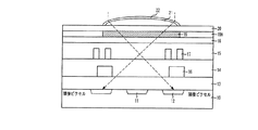
図2は、従来の技術に係るCMOSイメージセンサの単位画素の構造を示す断面図である。 FIG. 2 is a cross-sectional view showing the structure of a unit pixel of a CMOS image sensor according to the prior art.
図2に示されているように、従来の技術に係るCMOSイメージセンサの単位ピクセルの断面図には、基板10に形成された受光素子11上に層間絶縁膜13、14、15が順に形成されており、各層間絶縁膜13、14、15の間には配線16、17を備えている。ここで、符号12は素子分離膜を表す。
As shown in FIG. 2, in a cross-sectional view of a unit pixel of a CMOS image sensor according to the prior art, interlayer
また、層間絶縁膜の最上段には平坦化層18、20が形成されており、平坦化層18、20の間にはカラーフィルタ19が形成されている。
Further,
平坦化層20の上には、マイクロレンズ21が形成され、その上には低温絶縁保護膜22が形成されている。
A
従来の技術に係るCMOSイメージセンサは、受光素子11の上に配線16、17を形成し、その上にパッシべーション膜を形成する。その後、カラーフィルタ19を形成する前に平坦化処理を行い、カラーフィルタ19を形成し、再び平坦化処理を行う。
In a CMOS image sensor according to the prior art,
その後マイクロレンズ21を形成し、マイクロレンズ21を形成した後に低温絶縁保護膜22を塗布するが、それはマイクロレンズ21の主成分であるフォトレジスタ膜を外部汚染から保護し、特にバンプ工程において発生する金属エッチングダによる損傷を防止するためである。
Thereafter, the
しかし、入射光が低温絶縁保護膜22を通過してマイクロレンズ21を通る時、2つの物質の屈折率差が大きくないため、マイクロレンズ21の周縁部(以下、エッジとも記す)に入射する光は、受光素子11に集束されずに、ピクセル周囲の金属配線に入射することがしばしば発生する。
However, when incident light passes through the low-temperature insulating
すなわち、マイクロレンズ21のエッジを通過した光が受光素子11に集束されず、周囲の金属配線に達するか、さらには隣接したピクセルに達することがある。このことは、光感知部である受光素子11まで光が到達するまでの間に、隣接するピクセル間のクロストークを発生させ、光感度を減少させる原因となる場合がある。
That is, the light that has passed through the edge of the
本発明は、上述した問題を解決するためになされたものであって、その目的とするところは、マイクロレンズの保護のために形成する低温絶縁保護膜に起因するクロストークの発生を防止し、光感度の低下を防止できるCMOSイメージセンサ及びその製造方法を提供することにある。 The present invention has been made to solve the above-described problems, and its object is to prevent the occurrence of crosstalk due to the low-temperature insulating protective film formed for protecting the microlens, It is an object of the present invention to provide a CMOS image sensor that can prevent a decrease in photosensitivity and a method for manufacturing the same.
本発明によれば、受光素子と、該受光素子の上に形成されたマイクロレンズと、該マイクロレンズ上に形成され、該マイクロレンズを保護するための絶縁保護膜と、前記マイクロレンズと前記絶縁保護膜との間に形成され、前記マイクロレンズの屈折率よりも低い屈折率を有する酸化膜とを備えることを特徴とするCMOSイメージセンサを提供することができる。 According to the present invention, a light receiving element, a microlens formed on the light receiving element, an insulating protective film formed on the microlens to protect the microlens, the microlens and the insulating A CMOS image sensor comprising an oxide film formed between the protective film and having a refractive index lower than that of the microlens can be provided.
また、本発明は、CMOSイメージセンサの製造方法であって、基板上に受光素子を形成するステップと、該受光素子上にマイクロレンズを形成するステップと、該マイクロレンズの屈折率よりも小さい屈折率を有する酸化膜を前記マイクロレンズの上に形成するステップと、該マイクロレンズを保護するための絶縁保護膜を前記酸化膜上に形成するステップとを含むことを特徴とするCMOSイメージセンサの製造方法を提供することができる。 The present invention also relates to a method for manufacturing a CMOS image sensor, the step of forming a light receiving element on a substrate, the step of forming a microlens on the light receiving element, and a refraction smaller than the refractive index of the microlens. Forming an oxide film having a refractive index on the microlens; and forming an insulating protective film for protecting the microlens on the oxide film. A method can be provided.
本発明によれば、CMOSイメージセンサにおいて、マイクロレンズと低温絶縁保護膜との間に屈折率の低いSOG(SPIN ON GLASS)膜系列の酸化膜(屈折率n=1.41)を形成し、SOG膜とマイクロレンズとの屈折率差で入射光の屈折角度を調節して、入射光を最大限に受光素子に到達させることによって、光感度を向上させ、かつマイクロレンズの中央部とエッジ部との光感度差を低減することができる。 According to the present invention, in the CMOS image sensor, an oxide film (refractive index n = 1.41) of a low refractive index SOG (SPIN ON GLASS) film series is formed between the microlens and the low-temperature insulating protective film. By adjusting the refraction angle of incident light by the refractive index difference between the SOG film and the microlens, the incident light reaches the light receiving element as much as possible to improve the photosensitivity, and the central portion and the edge portion of the microlens Can be reduced.
本発明に係るCMOSイメージセンサは、入射光を最大限に受光素子に集束させ、単位ピクセルの光感度を向上させることができる。 The CMOS image sensor according to the present invention can focus the incident light to the light receiving element to the maximum and improve the light sensitivity of the unit pixel.
また、本発明に係るCMOSイメージセンサは、マイクロレンズの中央部とエッジ部との光感度差が低減し、より信頼性の高い、光に対するイメージ処理を可能にするという効果を奏する。 In addition, the CMOS image sensor according to the present invention has the effect of reducing the difference in light sensitivity between the central portion and the edge portion of the microlens and enabling image processing for light with higher reliability.
以下、本発明の最も好ましい実施の形態を添付する図面を参照して説明する。 Hereinafter, the most preferred embodiment of the present invention will be described with reference to the accompanying drawings.
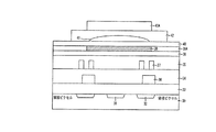
図3A〜図3Eは、本発明の好ましい実施の形態に係るCMOSイメージセンサの単位ピクセルの製造工程を示す断面図である。 3A to 3E are cross-sectional views illustrating a manufacturing process of a unit pixel of a CMOS image sensor according to a preferred embodiment of the present invention.
本実施の形態に係るCMOSイメージセンサは、図3Aに示されているように、先ず基板30上に受光素子31を形成する。
In the CMOS image sensor according to the present embodiment, a
次いで、複数の層間絶縁膜33、34、35と、それらの間の複数層の配線36、37とを形成する。
Next, a plurality of
次いで、平坦化膜38を形成し、受光素子31の上の所定領域にカラーフィルタ39を形成する。
Next, a
次いで、カラーフィルタ39上に平坦化膜40を形成する。
Next, a
次いで、カラーフィルタ39上にマイクロレンズ(屈折率n=1.592)41を形成する。次いで、マイクロレンズ41の表面を覆うように、SOG膜系列の酸化膜(波長450nmの光に対して屈折率n=1.41)42を形成する。ここで、酸化膜42は、コーディングによって、約4000〜5000Åの範囲の厚さに形成する。SOG膜系列の酸化膜の代わりに、屈折率nが1.5よりも小さい絶縁膜を使用することができる。
Next, a microlens (refractive index n = 1.593) 41 is formed on the
次いで、酸化膜42上に感光膜43を形成する。
Next, a
次いで、図3Bに示したように、マスク44(図3A参照)を用いて感光膜43を選択的に除去し、感光膜パターン43Aを形成する。
Next, as shown in FIG. 3B, the
次いで、図3Cに示したように、感光膜パターン43Aをエッチングマスクとして用い、酸化膜42を選択的に除去する。ここで、感光膜パターン43Aとしてネガティブ感光膜を用い、ピクセル部分だけをオープンするマスクを用いてピクセル以外の酸化膜42を選択的に除去する。図3Cにおいて、符号42Aは、感光膜パターン43Aをエッチングマスクとして用い、酸化膜42を選択的に除去した後に残存する酸化膜を表す。
Next, as shown in FIG. 3C, the
次いで、図3Dに示したように、感光膜パターン43Aを除去する。
Next, as shown in FIG. 3D, the
次いで、図3Eに示したように、残存する酸化膜42A上に低温絶縁保護膜45(波長450nmの光に対して屈折率n=1.55)を形成する。低温絶縁保護膜45は、約2000〜4000Åの範囲の厚さに形成する。
Next, as shown in FIG. 3E, a low-temperature insulating protective film 45 (refractive index n = 1.55 with respect to light having a wavelength of 450 nm) is formed on the remaining
0.18μmのデザインルールで形成したCMOSイメージセンサの場合、受光素子31の上に形成される絶縁層の段差が従来よりも減少することによって入射光量が増加し、光感度が改善されるが、上記したようにピクセルの中央部とエッジ部との光感度に差が生じることが問題となった。
In the case of a CMOS image sensor formed with a design rule of 0.18 μm, the step of the insulating layer formed on the
その原因には、単位ピクセルのエッジ部がデフォーカス(defocusing)される現象があり、これは入射光の光角度を調節すれば解決可能である。従って、本実施の形態に係るCMOSイメージセンサは、エッジ部への入射光が受光素子31にさらによく集束されるように、光の屈折角度を調節するものである。
The cause is a phenomenon that the edge portion of the unit pixel is defocused, which can be solved by adjusting the light angle of the incident light. Therefore, the CMOS image sensor according to the present embodiment adjusts the light refraction angle so that the incident light on the edge portion is more focused on the
本実施の形態に係るCMOSイメージセンサの単位ピクセルでは、低温絶縁保護膜45を通過した光がSOG膜系列の酸化膜42Aを経てマイクロレンズ41に入射する構造になっている。
The unit pixel of the CMOS image sensor according to the present embodiment has a structure in which light that has passed through the low-temperature insulating
マイクロレンズ41を通過した光は、受光素子31に集束するが、このとき受光素子41に光が集束する経路は、酸化膜42Aの屈折率とマイクロレンズ41の屈折率の大小関係に依存する。
The light that has passed through the
光が屈折率の異なる2つの物質(ここでは、酸化膜42A及びマイクロレンズ41)の境面を通過するときに、光路が境面と成す角度は、スネル(SNELL)の法則(ni×sinθi=nr×Sinθr)によって決まる。ここで、niは酸化膜42Aの屈折率、nrはマイクロレンズ41の屈折率である。また、θiは酸化膜42A中の光路(入射光)が界面の法線と成す角度、θrはマイクロレンズ41中の光路(屈折光)が界面の法線と成す角度である。したがって、マイクロレンズ41と酸化膜42Aの屈折率差が大きいほど、界面を通過した光はさらに屈折し、受光素子31にさらによく集束される。
When light passes through the boundary surface between two substances having different refractive indices (here, the
従来のCMOSイメージセンサの単位ピクセルでは、マイクロレンズ上に直接に絶縁保護膜が形成されており、低温絶縁保護膜とマイクロレンズとの屈折率差がそれほど大きくないため、これらの境面で光の屈折角が小さく、マイクロレンズを通過した光が受光素子に十分に集束されなかった。特に、エッジ部を通過した光の場合、その集束度が非常に悪かった。 In the unit pixel of the conventional CMOS image sensor, an insulating protective film is formed directly on the microlens, and the refractive index difference between the low-temperature insulating protective film and the microlens is not so large. The refraction angle was small, and the light that passed through the microlens was not sufficiently focused on the light receiving element. In particular, in the case of light passing through the edge portion, the degree of convergence was very poor.
これに対し、本実施の形態に係るCMOSイメージセンサでは、マイクロレンズ41と絶縁保護膜45との間にSOG膜系列の酸化膜42Aを備えているため、絶縁保護膜45を通過した光が絶縁保護膜45とマイクロレンズ41との界面を通過するときに、従来のCMOSイメージセンサよりも大きく屈折し、受光素子に到達し易くなる。従って、本実施の形態に係るCMOSイメージセンサでは、従来のCMOSイメージセンサよりも、入射光の集束能力が大きく向上する。
On the other hand, the CMOS image sensor according to the present embodiment includes the SOG film
マイクロレンズ41として用いる感光膜と屈折率の差が大きく、光をさらに効率的に集束させることができる材質の膜として、SOG膜系列の酸化膜があるが、マイクロレンズ41の屈折率(1.592)よりも低い屈折率(n<1.5)の材質の膜であれば、適用可能である。
As a film made of a material having a large difference in refractive index from the photosensitive film used as the
一方、上記のように酸化膜42Aの屈折率をマイクロレンズ41の屈折率よりも小さくすると、酸化膜42Aの上にある絶縁保護膜45の屈折率が、酸化膜42Aの屈折率よも相対的にさらに大きい値を有するようになる。
入射光がマイクロレンズ41に達する前に絶縁保護膜45と酸化膜42Aとを通過するので、屈折率が大きい物質である絶縁保護膜45から屈折率が小さい酸化膜42Aに入射するときに、光が受光素子から遠ざかる方向に屈折される可能性がある。しかし、光が酸化膜42Aと絶縁保護膜45との界面に対して垂直に入射する場合には、この現象を考慮する必要はない。
On the other hand, when the refractive index of the
Since the incident light passes through the insulating
したがって、上述した問題点が発生しないように、即ち、酸化膜42Aと絶縁保護膜45との界面に対して垂直に光が入射するように、本実施の形態では、マイクロレンズ41の表面を覆っている酸化膜42Aを平坦化し、その上に絶縁保護膜45を形成している。
Therefore, in the present embodiment, the surface of the
表1及び図4A〜図4Cは、図3A〜図3Eに示した方法で製造されたCMOSイメージセンサの単位ピクセルと、従来技術に係るCMOSイメージセンサの単位ピクセルとの光感度に関する実験データを示す。ここで、光感度は白色光の感度(white sensitivity)を意味する。 Table 1 and FIGS. 4A to 4C show experimental data on the photosensitivity between the unit pixel of the CMOS image sensor manufactured by the method shown in FIGS. 3A to 3E and the unit pixel of the CMOS image sensor according to the prior art. . Here, the photosensitivity means the sensitivity of white light (white sensitivity).
表1は、従来技術に係るCMOSイメージセンサの光感度に関するデータと、本実施の形態に係るCMOSイメージセンサの光感度に関する実験結果のデータを、赤(RED)、青(BLUE)、緑(GREEN)のフィルタに対応するピクセル毎に示している。また、エッジ部での光感度を、マイクロレンズの中央部での光感度を基準として、即ち、マイクロレンズの中央部での光感度に対する比率として示している。同様に、赤及び青の単位ピクセルの光感度を、緑の単位ピクセルの光感度を基準にして、即ち、緑の単位ピクセルの光感度に対する比率として示している。 Table 1 shows data on the photosensitivity of the CMOS image sensor according to the prior art and experimental result data on the photosensitivity of the CMOS image sensor according to the present embodiment. The data is red (RED), blue (BLUE), and green (GREEN). ) For each pixel corresponding to the filter. Further, the photosensitivity at the edge portion is shown based on the photosensitivity at the central portion of the microlens, that is, as a ratio to the photosensitivity at the central portion of the microlens. Similarly, the photosensitivity of the red and blue unit pixels is shown relative to the photosensitivity of the green unit pixel, ie, as a ratio to the photosensitivity of the green unit pixel.
「対照群」は、マイクロレンズ上に低温絶縁保護膜だけが形成された従来技術に係るCMOSイメージセンサに関するデータであり、「SOG蒸着実験群(以下、実験群とも記す)」は、マイクロレンズと絶縁保護膜との間にSOG膜系列の酸化膜が形成された本実施の形態に係るCMOSイメージセンサに関するデータである。 The “control group” is data relating to a CMOS image sensor according to the prior art in which only a low-temperature insulating protective film is formed on the microlens, and the “SOG deposition experiment group (hereinafter also referred to as experiment group)” is a microlens. This is data relating to the CMOS image sensor according to the present embodiment in which an SOG film series oxide film is formed between the insulating protective film.

図4Aは、従来技術に係るCMOSイメージセンサと本実施の形態に係るCMOSイメージセンサの赤、青、緑の各単位ピクセルにおける、マイクロレンズの中央部での光感度に関するデータを示すグラフである。図4Bは、マイクロレンズのエッジ部での光感度に関するデータを示すグラフである。 FIG. 4A is a graph showing data relating to photosensitivity at the center of the microlens in each of the red, blue, and green unit pixels of the CMOS image sensor according to the related art and the CMOS image sensor according to the present embodiment. FIG. 4B is a graph showing data relating to light sensitivity at the edge portion of the microlens.
図4Cは、図4A及び図4Bのデータを共に示したグラフである。 FIG. 4C is a graph showing both the data of FIGS. 4A and 4B.
まず、マイクロレンズの中央部における光感度について述べると、緑と赤のピクセルの場合、対照群と実験群との光感度差に大きな違いがないことが分かる。表1を参照すると、対照群では、緑のピクセルの光感度は731mV/lux secないし733mV/lux sec、赤のピクセルの光感度は464mV/lux secないし468mV/lux secであった。実験群では、緑のピクセルの光感度は705mV/lux secないし733、赤のピクセルの光感度は457mV/lux secないし477mV/lux secである。 First, regarding the photosensitivity at the center of the microlens, it can be seen that there is no significant difference in the photosensitivity between the control group and the experimental group in the case of green and red pixels. Referring to Table 1, in the control group, the light sensitivity of the green pixel was 731 mV / lux sec to 733 mV / lux sec, and the light sensitivity of the red pixel was 464 mV / lux sec to 468 mV / lux sec. In the experimental group, the light sensitivity of the green pixel is 705 mV / lux sec to 733, and the light sensitivity of the red pixel is 457 mV / lux sec to 477 mV / lux sec.
また、青のピクセルに関しては、実験群の光感度が対照群の光感度よりも約60〜80mV/lux sec程度減少した。青のピクセルの光感度は、対照群では557mV/lux secないし553mV/lux secであり、実験群では466mV/lux secないし485mV/lux secである。 For the blue pixel, the photosensitivity of the experimental group decreased by about 60 to 80 mV / lux sec than the photosensitivity of the control group. The light sensitivity of the blue pixel is 557 mV / lux sec to 553 mV / lux sec in the control group and 466 mV / lux sec to 485 mV / lux sec in the experimental group.
光感度比に関しては、実験群の場合、緑のピクセルに対する青のピクセルの光感度比、緑のピクセルに対する赤のピクセルの光感度比がほぼ同じ値である。 Regarding the photosensitivity ratio, in the experimental group, the photosensitivity ratio of the blue pixel to the green pixel and the photosensitivity ratio of the red pixel to the green pixel are approximately the same value.
一般的に、CMOSイメージセンサにおいて、緑のピクセルに対する赤ピクセルの光感度比と、緑のピクセルに対する青のピクセルの光感度比は、近似していることが好ましい。これは、CMOSイメージセンサの特徴上、単位ピクセルの総数の50%を占める緑のピクセルに対して、赤のピクセルと青のピクセルとが同じ程度の感度でなければ、画質が良くないからである。 In general, in the CMOS image sensor, it is preferable that the light sensitivity ratio of the red pixel to the green pixel and the light sensitivity ratio of the blue pixel to the green pixel are approximate. This is because, due to the characteristics of the CMOS image sensor, the image quality is not good unless the red and blue pixels have the same sensitivity with respect to the green pixels that occupy 50% of the total number of unit pixels. .
本実施の形態に係るCMOSイメージセンサは、マイクロレンズのエッジ部に入射する光を受光素子に集めるために、屈折率がマイクロレンズよりも低い酸化膜を備えている。その結果、緑のピクセルに対する赤のピクセルの光感度比と、緑のピクセルに対する青のピクセルの光感度比とが、近い値となり、CMOSイメージセンサの特性が向上した。 The CMOS image sensor according to the present embodiment includes an oxide film having a refractive index lower than that of the microlens in order to collect light incident on the edge portion of the microlens on the light receiving element. As a result, the light sensitivity ratio of the red pixel to the green pixel and the light sensitivity ratio of the blue pixel to the green pixel are close to each other, and the characteristics of the CMOS image sensor are improved.
一方、マイクロレンズのエッジ領域での光感度について述べると、緑と赤のピクセルの場合、実験群は対照群に比べて光感度が約100mV/lux sec増大していることが分かる。対照群では、緑のピクセルの光感度は308mV/lux secないし314mV/lux sec、赤のピクセルの光感度は228mV/lux secないし234mV/lux secであり、実験群では、緑のピクセルの光感度は398mV/lux secないし412mV/lux sec、赤のピクセルの光感度は327mV/lux secないし339mV/lux secである。 On the other hand, regarding the photosensitivity in the edge region of the microlens, it can be seen that in the case of green and red pixels, the photosensitivity of the experimental group is increased by about 100 mV / lux sec compared to the control group. In the control group, the light sensitivity of the green pixel is 308 mV / lux sec to 314 mV / lux sec, the light sensitivity of the red pixel is 228 mV / lux sec to 234 mV / lux sec, and in the experimental group, the light sensitivity of the green pixel Is 398 mV / lux sec to 412 mV / lux sec, and the red pixel has a photosensitivity of 327 mV / lux sec to 339 mV / lux sec.
また、青のピクセルの光感度については、実験群が対照群よりも約60mV/lux sec増大している。したがって、約100mV/lux sec増大した赤のピクセルに対して、青のピクセルでは、約40mV/lux secと増大の程度が小さいので、相対的に青のピクセルの光感度が赤のピクセルと近い値になった。 Moreover, about the photosensitivity of a blue pixel, the experimental group has increased about 60 mV / lux sec than the control group. Therefore, since the degree of increase is small at about 40 mV / lux sec for the blue pixel compared to the red pixel increased by about 100 mV / lux sec, the light sensitivity of the blue pixel is relatively close to that of the red pixel. Became.
したがって、実験群の場合、緑のピクセルに対する青のピクセルの光感度比と、緑のピクセルに対する赤のピクセルの光感度比がほぼ近い値になった。 Therefore, in the case of the experimental group, the light sensitivity ratio of the blue pixel to the green pixel and the light sensitivity ratio of the red pixel to the green pixel were almost close to each other.
これを整理すると、本実施の形態に係るCMOSイメージセンサにおいてマイクロレンズ41と絶縁保護膜45との間にSOG膜系列の酸化膜42Aを形成することによって、マイクロレンズ41の中央部での光感度を変化させずに、エッジ部での光感度を大きく増大させることができる。マイクロレンズ41のエッジ部において、赤のピクセルと緑のピクセルの光感度は約100mV/lux sec増大し、青のピクセルの光感度は約60mV/lux sec増大する。
In summary, in the CMOS image sensor according to the present embodiment, the SOG film
また、マイクロレンズ41と絶縁保護膜45との間の酸化膜42Aは、緑のピクセルに対する青のピクセルの光感度比が、緑のピクセルに対する赤のピクセルの光感度比に近い値になるように、青のピクセルの光感度をシフトさせる役割も担っている。
Further, the
尚、本発明は、上記した実施の形態に限定されるものではなく、本発明に係る技術的思想から逸脱しない範囲内で様々な変更が可能であり、それらも本発明の技術的範囲に属する。 The present invention is not limited to the above-described embodiments, and various modifications are possible without departing from the technical idea according to the present invention, and these also belong to the technical scope of the present invention. .
Claims (20)
該受光素子の上に形成されたマイクロレンズと、
該マイクロレンズの上に形成され、該マイクロレンズを保護するための絶縁保護膜と、
前記マイクロレンズと前記絶縁保護膜との間に形成され、前記マイクロレンズの屈折率よりも小さい屈折率を有する酸化膜と
を備えることを特徴とするCMOSイメージセンサ。 A light receiving element;
A microlens formed on the light receiving element;
An insulating protective film formed on the microlens for protecting the microlens;
A CMOS image sensor comprising: an oxide film formed between the microlens and the insulating protective film and having a refractive index smaller than that of the microlens.
複数層の前記配線を相互に絶縁するための層間絶縁膜とをさらに備えることを特徴とする請求項9に記載のCMOSイメージセンサ。 A plurality of layers of wiring formed between the light receiving element and the color filter layer;
The CMOS image sensor according to claim 9, further comprising an interlayer insulating film for insulating the wirings of a plurality of layers from each other.
基板上に受光素子を形成するステップと、
該受光素子上にマイクロレンズを形成するステップと、
該マイクロレンズの屈折率よりも小さい屈折率を有する酸化膜を前記マイクロレンズの上に形成するステップと、
該マイクロレンズを保護するための絶縁保護膜を前記酸化膜の上に形成するステップと
を含むことを特徴とするCMOSイメージセンサの製造方法。 A CMOS image sensor manufacturing method comprising:
Forming a light receiving element on the substrate;
Forming a microlens on the light receiving element;
Forming an oxide film on the microlens having a refractive index smaller than that of the microlens;
Forming an insulating protective film on the oxide film for protecting the microlens.
Applications Claiming Priority (1)
| Application Number | Priority Date | Filing Date | Title |
|---|---|---|---|
| KR1020040072280A KR100694468B1 (en) | 2004-09-09 | 2004-09-09 | Cmos image sensor and method for fabricating the same |
Publications (1)
| Publication Number | Publication Date |
|---|---|
| JP2006080480A true JP2006080480A (en) | 2006-03-23 |
Family
ID=36159652
Family Applications (1)
| Application Number | Title | Priority Date | Filing Date |
|---|---|---|---|
| JP2005066893A Pending JP2006080480A (en) | 2004-09-09 | 2005-03-10 | Complementary metal oxide semiconductor image sensors and its manufacturing method |
Country Status (4)
| Country | Link |
|---|---|
| US (1) | US20060049412A1 (en) |
| JP (1) | JP2006080480A (en) |
| KR (1) | KR100694468B1 (en) |
| TW (1) | TW200610141A (en) |
Families Citing this family (7)
| Publication number | Priority date | Publication date | Assignee | Title |
|---|---|---|---|---|
| KR100812088B1 (en) * | 2006-12-27 | 2008-03-07 | 동부일렉트로닉스 주식회사 | Method for forming micro-lense of cmos image sensor |
| US8779540B2 (en) * | 2011-01-26 | 2014-07-15 | Maxim Integrated Products, Inc. | Light sensor having transparent substrate with lens formed therein |
| US8803068B2 (en) | 2011-01-26 | 2014-08-12 | Maxim Integrated Products, Inc. | Light sensor having a contiguous IR suppression filter and a transparent substrate |
| US8624341B2 (en) | 2011-01-26 | 2014-01-07 | Maxim Integrated Products, Inc. | Light sensor having IR cut and color pass interference filter integrated on-chip |
| US8598672B2 (en) | 2011-01-26 | 2013-12-03 | Maxim Integrated Products, Inc | Light sensor having IR cut interference filter with color filter integrated on-chip |
| US10490585B1 (en) * | 2018-05-14 | 2019-11-26 | Semiconductor Components Industries, Llc | Imaging pixels with plasmonic color filter elements |
| US10847564B1 (en) | 2019-07-24 | 2020-11-24 | Taiwan Semiconductor Manufacturing Co., Ltd. | Charge release layer to remove charge carriers from dielectric grid structures in image sensors |
Citations (1)
| Publication number | Priority date | Publication date | Assignee | Title |
|---|---|---|---|---|
| JPH06232379A (en) * | 1993-02-01 | 1994-08-19 | Sharp Corp | Solid-state image pickup element |
Family Cites Families (4)
| Publication number | Priority date | Publication date | Assignee | Title |
|---|---|---|---|---|
| JPH10270672A (en) * | 1997-03-25 | 1998-10-09 | Sony Corp | Solid-state image pickup element |
| KR100533166B1 (en) * | 2000-08-18 | 2005-12-02 | 매그나칩 반도체 유한회사 | CMOS image sensor having low temperature oxide for protecting microlens and method for fabricating the same |
| KR20020048706A (en) * | 2000-12-18 | 2002-06-24 | 박종섭 | Image sensor having OCM layer over microlens and method for fabricating the same |
| TW513809B (en) * | 2002-02-07 | 2002-12-11 | United Microelectronics Corp | Method of fabricating an image sensor |
-
2004
- 2004-09-09 KR KR1020040072280A patent/KR100694468B1/en not_active IP Right Cessation
-
2005
- 2005-03-03 US US11/072,674 patent/US20060049412A1/en not_active Abandoned
- 2005-03-10 JP JP2005066893A patent/JP2006080480A/en active Pending
- 2005-03-11 TW TW094107599A patent/TW200610141A/en unknown
Patent Citations (1)
| Publication number | Priority date | Publication date | Assignee | Title |
|---|---|---|---|---|
| JPH06232379A (en) * | 1993-02-01 | 1994-08-19 | Sharp Corp | Solid-state image pickup element |
Also Published As
| Publication number | Publication date |
|---|---|
| KR100694468B1 (en) | 2007-03-12 |
| KR20060023435A (en) | 2006-03-14 |
| TW200610141A (en) | 2006-03-16 |
| US20060049412A1 (en) | 2006-03-09 |
Similar Documents
| Publication | Publication Date | Title |
|---|---|---|
| TWI742573B (en) | Solid-state imaging element, its manufacturing method, and electronic equipment | |
| US7545423B2 (en) | Image sensor having a passivation layer exposing at least a main pixel array region and methods of fabricating the same | |
| TWI636557B (en) | Solid-state imaging device, manufacturing method thereof, and electronic device | |
| US10700113B2 (en) | Image sensors with diffractive lenses for stray light control | |
| US7579209B2 (en) | Image sensor and fabricating method thereof | |
| US10804306B2 (en) | Solid-state imaging devices having flat microlenses | |
| US8030117B2 (en) | Image sensor and method for manufacturing the same | |
| JP2006080480A (en) | Complementary metal oxide semiconductor image sensors and its manufacturing method | |
| KR100685882B1 (en) | CMOS Image Sensor | |
| KR102223515B1 (en) | Solid-state imaging device and electronic device | |
| KR100801850B1 (en) | Image sensor and method of manufacturing the same | |
| US20090321864A1 (en) | Cmos image sensor and method for manufacturing the sensor | |
| JP6300564B2 (en) | Solid-state imaging device and manufacturing method thereof | |
| JP2013016702A (en) | Solid-state imaging device and camera module | |
| KR20020045162A (en) | Image sensor having microlens made of oxide layer and method for forming the same | |
| KR100873290B1 (en) | CMOS image sensor with double microlens | |
| KR100410669B1 (en) | Image sensor and fabricating method of the same | |
| US20090068599A1 (en) | Method of manufacturing image sensor | |
| US7563626B2 (en) | Manufacturing method of complementary metal oxide silicon image sensor | |
| KR100749265B1 (en) | Image sensor | |
| KR100658928B1 (en) | Method for fabricating cmos image sensor | |
| KR100381025B1 (en) | Image sensor having trench for capturing impurity and method for forming the same | |
| KR20060020852A (en) | Cmos image sensor and method for fabricating the same | |
| KR20050039160A (en) | Image sensor having color filter used for inner lens and the fabricating method thereof | |
| KR20060004824A (en) | Cmos image sensor |
Legal Events
| Date | Code | Title | Description |
|---|---|---|---|
| A621 | Written request for application examination |
Free format text: JAPANESE INTERMEDIATE CODE: A621 Effective date: 20080229 |
|
| A711 | Notification of change in applicant |
Free format text: JAPANESE INTERMEDIATE CODE: A711 Effective date: 20090630 |
|
| A977 | Report on retrieval |
Free format text: JAPANESE INTERMEDIATE CODE: A971007 Effective date: 20110713 |
|
| A131 | Notification of reasons for refusal |
Free format text: JAPANESE INTERMEDIATE CODE: A131 Effective date: 20110715 |
|
| A711 | Notification of change in applicant |
Free format text: JAPANESE INTERMEDIATE CODE: A712 Effective date: 20110928 |
|
| A02 | Decision of refusal |
Free format text: JAPANESE INTERMEDIATE CODE: A02 Effective date: 20120131 |