JP2006066199A - Self-emitting flat panel display device and its manufacturing method - Google Patents
Self-emitting flat panel display device and its manufacturing method Download PDFInfo
- Publication number
- JP2006066199A JP2006066199A JP2004246814A JP2004246814A JP2006066199A JP 2006066199 A JP2006066199 A JP 2006066199A JP 2004246814 A JP2004246814 A JP 2004246814A JP 2004246814 A JP2004246814 A JP 2004246814A JP 2006066199 A JP2006066199 A JP 2006066199A
- Authority
- JP
- Japan
- Prior art keywords
- electrode
- metal film
- insulating film
- electrode lead
- lead terminal
- Prior art date
- Legal status (The legal status is an assumption and is not a legal conclusion. Google has not performed a legal analysis and makes no representation as to the accuracy of the status listed.)
- Pending
Links
Images


Classifications
-
- H—ELECTRICITY
- H01—ELECTRIC ELEMENTS
- H01J—ELECTRIC DISCHARGE TUBES OR DISCHARGE LAMPS
- H01J9/00—Apparatus or processes specially adapted for the manufacture, installation, removal, maintenance of electric discharge tubes, discharge lamps, or parts thereof; Recovery of material from discharge tubes or lamps
- H01J9/24—Manufacture or joining of vessels, leading-in conductors or bases
- H01J9/32—Sealing leading-in conductors
-
- H—ELECTRICITY
- H01—ELECTRIC ELEMENTS
- H01J—ELECTRIC DISCHARGE TUBES OR DISCHARGE LAMPS
- H01J29/00—Details of cathode-ray tubes or of electron-beam tubes of the types covered by group H01J31/00
- H01J29/90—Leading-in arrangements; Seals therefor
-
- H—ELECTRICITY
- H01—ELECTRIC ELEMENTS
- H01J—ELECTRIC DISCHARGE TUBES OR DISCHARGE LAMPS
- H01J31/00—Cathode ray tubes; Electron beam tubes
- H01J31/08—Cathode ray tubes; Electron beam tubes having a screen on or from which an image or pattern is formed, picked up, converted, or stored
- H01J31/10—Image or pattern display tubes, i.e. having electrical input and optical output; Flying-spot tubes for scanning purposes
- H01J31/12—Image or pattern display tubes, i.e. having electrical input and optical output; Flying-spot tubes for scanning purposes with luminescent screen
- H01J31/123—Flat display tubes
-
- H—ELECTRICITY
- H01—ELECTRIC ELEMENTS
- H01J—ELECTRIC DISCHARGE TUBES OR DISCHARGE LAMPS
- H01J9/00—Apparatus or processes specially adapted for the manufacture, installation, removal, maintenance of electric discharge tubes, discharge lamps, or parts thereof; Recovery of material from discharge tubes or lamps
- H01J9/24—Manufacture or joining of vessels, leading-in conductors or bases
- H01J9/26—Sealing together parts of vessels
- H01J9/261—Sealing together parts of vessels the vessel being for a flat panel display
Abstract
Description
本発明は、真空中への電子放出を利用した表示装置に係り、特に、電子を放出する電子源を有する背面パネルと、背面パネルから取り出された電子の励起で発光する複数色の蛍光体層と電子加速電極を有する前面パネルとを封止枠で封止した表示パネルを具備した自発光平面表示装置とその製造方法に関する。 The present invention relates to a display device using electron emission into a vacuum, and in particular, a back panel having an electron source that emits electrons, and a plurality of color phosphor layers that emit light by excitation of electrons extracted from the back panel. The present invention relates to a self-luminous flat panel display device including a display panel in which a front panel having an electron acceleration electrode and a front panel are sealed with a sealing frame, and a manufacturing method thereof.
高輝度、高精細に優れたディスプレイデバイスとして従来からカラー陰極線管が広く用いられている。しかし、近年の情報処理装置やテレビ放送の高画質化に伴い、高輝度、高精細の特性をもつと共に軽量、省スペースの平面型表示装置の要求が高まっている。 Conventionally, a color cathode ray tube has been widely used as a display device excellent in high luminance and high definition. However, with the recent improvement in image quality of information processing devices and television broadcasting, there is an increasing demand for flat display devices that have high brightness and high definition characteristics, light weight, and space saving.
その典型例として液晶表示装置、プラズマ表示装置などが実用化されている。また、特に、高輝度化が可能なものとして、電子源から真空への電子放出を利用した電子放出型表示装置、または電界放出型表示装置や、低消費電力を特徴とする有機ELディスプレイなど、種々の型式のパネル型表示装置の実用化も近い。なお、補助的な照明光源を必要としないプラズマ表示装置、電子放出型表示装置あるいは有機EL表示装置を自発光平面表示装置と称する。 As typical examples, liquid crystal display devices, plasma display devices and the like have been put into practical use. In particular, it is possible to increase the brightness, such as an electron emission display device using electron emission from an electron source to a vacuum, or a field emission display device, an organic EL display characterized by low power consumption, etc. Various types of panel-type display devices will soon be put into practical use. A plasma display device, an electron emission display device or an organic EL display device that does not require an auxiliary illumination light source is referred to as a self-luminous flat display device.
このような自発光平面表示装置のうち、電子放出型の表示装置には、C.A.Spindtらにより発案されたコーン状の電子放出構造をもつもの、メタル−インシュレータ−メタル(MIM)型の電子放出構造をもつもの、量子論的トンネル効果による電子放出現象を利用する電子放出構造(表面伝導型電子源とも呼ばれる)をもつもの、さらにはダイアモンド膜やグラファイト膜、カーボンナノチューブに代表されるナノチューブなどが持つ電子放出現象を利用するもの、等が知られている。 Among such self-luminous flat display devices, an electron emission display device includes C.I. A. Spindt et al., Conical electron emission structure, metal-insulator-metal (MIM) type electron emission structure, electron emission structure using electron emission phenomenon due to quantum tunnel effect (surface Also known are those having a conduction electron source, and those utilizing the electron emission phenomenon of diamond films, graphite films, nanotubes typified by carbon nanotubes, and the like.
自発光平面表示装置の一例である電子放出型の表示装置を構成する表示パネルは、内面に電小放出型の電子源を有する第1電極(例えば、カソード電極)と制御電極である第2電極(例えば、ゲート電極、走査電極)を形成した背面パネルと、この背面パネルと対向する内面に複数色の蛍光体層と第3電極(アノード電極、陽極)とを備えた前面パネルを有している。前面パネルは、ガラスを好適とする光透過性の材料で形成される。そして、両パネルの貼り合せ内周縁に封止枠を介挿して封止し、当該背面パネルと前面パネルおよび封止枠で形成される内部を真空にして構成される。背面パネルには、ガラスあるいはアルミナ等の絶縁材を好適とする背面基板の上に、第1の方向に延在しこの第1の方向と交差する第2の方向に並設されて多数の電子源をもつ複数の第1電極と、第2の方向に延在し第1の方向に並設して設けた第2電極を有する。 A display panel constituting an electron emission type display device which is an example of a self-luminous flat display device has a first electrode (for example, a cathode electrode) having a small emission type electron source on the inner surface and a second electrode which is a control electrode. (E.g., a back panel having a gate electrode and a scan electrode), and a front panel having a plurality of color phosphor layers and a third electrode (anode electrode, anode) on the inner surface facing the back panel. Yes. The front panel is formed of a light transmissive material, preferably glass. And it seals by inserting the sealing frame in the bonding inner periphery of both panels, and the inside formed with the said back panel, front panel, and sealing frame is made into a vacuum. The back panel has a large number of electrons arranged in parallel in a second direction extending in a first direction and intersecting the first direction on a back substrate preferably made of an insulating material such as glass or alumina. A plurality of first electrodes having a source and a second electrode extending in the second direction and arranged in parallel in the first direction.
電子源は第1電極と第2電極の交差部に有し、第1電極と第2電極との間の電位差で電子源からの電子の放出量(放出のオン・オフを含む)を制御する。放出された電子は、前面パネルに有する陽極に印加される高電圧で加速され、同じく前面パネルに有する蛍光体層に射突して励起することで当該蛍光体層の発光特性に応じた色光で発色する。 The electron source has an intersection of the first electrode and the second electrode, and controls the amount of electrons emitted from the electron source (including emission on / off) by the potential difference between the first electrode and the second electrode. . The emitted electrons are accelerated by a high voltage applied to the anode provided on the front panel, and are projected and excited by the phosphor layer also provided on the front panel, so that the emitted light is colored with light corresponding to the emission characteristics of the phosphor layer. Color develops.
また、封止枠は背面パネルと前面パネルとの内周縁にフリットガラスなどの接着材で固着される。背面パネルと前面パネルおよび封止枠で形成される内部の真空度は、例えば10-5〜10-7Torrである。表示面サイズが大きいものでは、背面パネルと前面パネルの間に間隙保持部材(スペーサ)を介挿して固定し、両基板間の間を所定の間隔に保持している。 The sealing frame is fixed to the inner peripheral edge of the back panel and the front panel with an adhesive such as frit glass. The internal degree of vacuum formed by the back panel, the front panel, and the sealing frame is, for example, 10 −5 to 10 −7 Torr. In the case where the display surface size is large, a gap holding member (spacer) is interposed between the rear panel and the front panel, and the gap between the two substrates is held at a predetermined interval.
封止枠と背面パネルの間には、背面パネルに形成された第1電極につながる第1電極引出端子や第2電極につながる第2電極引出端子が存在する。通常、封止枠はフリットガラスなどの接着剤で背面パネルおよび前面パネルに固着される。第1電極引出端子や第2電極引出端子が封止枠と背面パネルの接着部である封止領域を通して引き出されており、この封止領域から真空のリークが発生し易い。このような真空のリークを対策する手段の例は、特許文献1に開示がある。
第1電極と第2電極の間を絶縁する絶縁膜(以下、層間絶縁膜とも称する)は上記の封止領域に存在している、第1電極(および第1電極引出端子)と第2電極(および第2電極引出端子)の間に存在する絶縁膜(層間絶縁膜)の中には、封止枠を固着するフリットガラスなどの接着剤との間で化学反応を起こして封止領域から真空のリークを促進するものがある。典型例としては、この絶縁膜に窒化シリコン(SiN)を用い、封止枠の固着にフリットガラス(PbO系)を用いた場合、PbO+SiN→Pb+SiO2+NO(ガス)の反応が生じ、このガス(NO)が泡としてフリットガラスに閉じ込められることで接着部分が脆くなり、かつ気密性を低下させる。気密性が低下する結果、背面パネルと前面パネルおよび封止枠で構成される内部空間の真空度が劣化し、自発光平面表示装置の信頼性を損なう。 An insulating film (hereinafter also referred to as an interlayer insulating film) that insulates between the first electrode and the second electrode is present in the sealing region, and the first electrode (and the first electrode lead terminal) and the second electrode In the insulating film (interlayer insulating film) existing between (and the second electrode lead-out terminal), a chemical reaction is caused with an adhesive such as frit glass that fixes the sealing frame, and from the sealing region. Some promote vacuum leaks. As a typical example, when silicon nitride (SiN) is used for the insulating film and frit glass (PbO system) is used for fixing the sealing frame, a reaction of PbO + SiN → Pb + SiO 2 + NO (gas) occurs, and this gas ( When NO) is trapped in the frit glass as bubbles, the bonded portion becomes brittle and airtightness is lowered. As a result of the reduced airtightness, the degree of vacuum in the internal space formed by the back panel, the front panel, and the sealing frame deteriorates, and the reliability of the self-luminous flat panel display device is impaired.
本発明の目的は、層間絶縁膜と封止枠の接着剤との反応に起因する真空度の劣化の発生を抑制し、信頼性の高い表示パネルを具備した自発光平面表示装置とその製造方法を提供することにある。 An object of the present invention is to suppress the occurrence of deterioration in vacuum due to the reaction between an interlayer insulating film and an adhesive of a sealing frame, and to provide a self-luminous flat panel display device including a highly reliable display panel and a method for manufacturing the same Is to provide.
上記目的を達成するための本発明の手段1は、背面パネルの第1電極および第1電極引出端子(以下、単に第1電極とも記す)と第2電極および第2電極引出端子(以下、単に第2電極とも記す)の間に有する絶縁膜(層間絶縁膜)を、前面パネルとの封止領域を除いて形成し(封止領域には絶縁膜を存在させない)、封止領域の第2電極引出し側においては封止枠と背面パネルの間には背面パネルと封止枠とを接着する接着剤の層と第2電極引出端子のみが存在するようにした。また、同じく本発明の手段2は、封止領域における第2電極引出端子の下層の該層間絶縁膜を残し、該第2電極引出端子の間には該層間絶縁膜を有しない構成とした。さらに、同じく本発明の手段3は、上記手段2において、封止領域における第2電極引出端子の下層の該層間絶縁膜を残す場合に、該第2電極引出端子の少なくとも一方の側縁の長さを該第2電極引出端子の上記封止領域における引き出し距離よりも長い平面形状とした。
なお、封止領域の第1電極引出し側についても、手段1と同様に封止領域の層間絶縁膜を除去することで封止枠の接着剤と層間絶縁膜の接触を回避することができる。
これらの構成とした表示パネルに画像信号駆動回路、走査信号駆動回路、その他の周辺回路を組み込んで自発光平面表示装置を構成する。
Note that also on the first electrode lead side of the sealing region, contact between the adhesive of the sealing frame and the interlayer insulating film can be avoided by removing the interlayer insulating film in the sealing region in the same manner as the
A self-luminous flat panel display is configured by incorporating an image signal driving circuit, a scanning signal driving circuit, and other peripheral circuits into the display panel having such a configuration.
本発明の手段1によれば、第1電極と第2電極を絶縁する層間絶縁膜と背面パネルに封止枠を接着する接着剤との接触が完全に回避され、両者の化学反応に起因する真空リークは防止され、この接触に起因する真空リークを防止することができる。また、本発明の手段2によれば、第1電極と第2電極を絶縁する層間絶縁膜と背面パネルに封止枠を接着する接着剤との接触部位は第2電極(第2電極引出端子)の下層に存在する層間絶縁膜の側面であるため、両者の接触による化学反応は極めて限定されたものとなり、この接触に起因する真空リークを防止することができる。さらに、本発明の手段3によれば、手段2における層間絶縁膜の側面と封止枠を接着する接着剤との接触距離が長くなることで、真空リークの可能性を低減できる。
According to the
なお、手段1において、手段3と同様に第2電極引出端子の少なくとも一方の端縁の長さを該第2電極引出端子の引き出し距離よりも長い平面形状とすることで、さらに真空リークの可能性を低減できる。なお、上記手段1の構成を第1電極(第1電極引出端子)についても同様に適用できることは言うまでもない。
In the
以下、本発明の実施の形態について、図面を参照して詳細に説明する。まず、本発明の実施例1を図1により説明する。
Hereinafter, embodiments of the present invention will be described in detail with reference to the drawings. First,
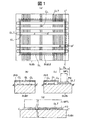
図1は、本発明の自発光平面表示装置を構成する表示パネルの実施例1を説明する模式図であり、図1(a)は背面パネルの内面構成を説明する平面図、図1(b)は図1(a)のA−A’線に沿った部分断面図、図1(c)は図1(a)のB−B’線に沿った部分断面図、図1(d)は図1(a)のC−C’線に沿った部分断面図である。なお、図1(a)の平面図では、前面パネルについて、その基板(前面基板)SUB2の外形の位置を示す破線で表してある。背面パネルと前面パネルは、両者の外周内縁に封止枠MFLを介在させ、接着剤としてフリットガラスFGで接着されて一体化されている。封止枠MFLでの封止領域を符号SLで示してある。 FIG. 1 is a schematic view for explaining Example 1 of a display panel constituting a self-luminous flat display device of the present invention, FIG. 1 (a) is a plan view for explaining the inner surface configuration of a back panel, and FIG. ) Is a partial cross-sectional view taken along line AA ′ in FIG. 1A, FIG. 1C is a partial cross-sectional view taken along line BB ′ in FIG. 1A, and FIG. It is a fragmentary sectional view along CC 'line of Fig.1 (a). In the plan view of FIG. 1A, the front panel is represented by a broken line indicating the position of the outer shape of the substrate (front substrate) SUB2. The back panel and the front panel are integrated by adhering a sealing frame MFL to the inner peripheral edge of both of them and bonding them with frit glass FG as an adhesive. A sealing region in the sealing frame MFL is indicated by reference sign SL.
背面パネルには、背面基板SUB1の上に第1電極CLと第2電極GLが形成されている。図1において、第1電極CLの端部には第1電極引出端子CLTを有し、第2電極GLの端部には第2電極引出端子GLTを有する。以下の実施例では、第1電極CLをカソード電極CL、第1電極引出端子CLTをカソード電極引出端子CLT、第2電極GLをゲート電極GL、第2電極引出端子GLTをゲート電極引出端子GLTとして説明する。 In the back panel, the first electrode CL and the second electrode GL are formed on the back substrate SUB1. In FIG. 1, the end of the first electrode CL has a first electrode lead terminal CLT, and the end of the second electrode GL has a second electrode lead terminal GLT. In the following embodiments, the first electrode CL is the cathode electrode CL, the first electrode lead terminal CLT is the cathode electrode lead terminal CLT, the second electrode GL is the gate electrode GL, and the second electrode lead terminal GLT is the gate electrode lead terminal GLT. explain.
カソード電極CLはストライプ状電極であり、背面基板SUB1上の第1の方向(図の縦方向)に延在して第1の方向と交差する第2の方向(図の横方向)に多数並設されている。このカソード電極CLの上を覆って絶縁膜(層間絶縁膜)INSが形成されている。この絶縁膜INS上で上記第2の方向に延在して上記第1の方向に多数のゲート電極GLが並設されている。ゲート電極GLもストライプ状電極である。カソード電極CLの端部にはカソード電極引出端子CLTが形成されている。図1(a)には、このカソード電極引出端子CLTがカソード電極CLの両端に設けられるものとして示されているが、何れか一端のみに形成してもよい。 The cathode electrode CL is a striped electrode, and extends in the first direction (vertical direction in the figure) on the back substrate SUB1 and is arranged in parallel in a second direction (horizontal direction in the figure) intersecting the first direction. It is installed. An insulating film (interlayer insulating film) INS is formed so as to cover the cathode electrode CL. On the insulating film INS, a large number of gate electrodes GL are arranged in parallel in the first direction so as to extend in the second direction. The gate electrode GL is also a striped electrode. A cathode electrode lead terminal CLT is formed at the end of the cathode electrode CL. Although FIG. 1A shows the cathode electrode lead terminals CLT provided at both ends of the cathode electrode CL, the cathode electrode lead terminals CLT may be formed only at one end.
同様に、ゲート電極GLの端部にはゲート電極引出端子GLTが形成されている。このゲート電極引出端子GLTがゲート電極GLの両端に設けられるものとして示されているが、何れか一端のみに形成してもよい。 Similarly, a gate electrode lead terminal GLT is formed at the end of the gate electrode GL. Although the gate electrode lead terminal GLT is shown as being provided at both ends of the gate electrode GL, it may be formed only at one end.
封止領域SLの内側は表示領域であり、この表示領域内のカソード電極CLとゲート電極GLの各交差部には電子源が配置される。電子源は、例えば、後述するような構成を有するMIM電子源である。そして、この電子源は、ゲート電極引出端子GLTから順次入力する垂直走査信号で選択されたゲート電極GLと交差するカソード電極CLに対してカソード電極引出端子CLTから供給される画像データに応じた電子量を放出する。 Inside the sealing region SL is a display region, and an electron source is arranged at each intersection of the cathode electrode CL and the gate electrode GL in the display region. The electron source is, for example, a MIM electron source having a configuration as described later. This electron source is an electron corresponding to image data supplied from the cathode electrode lead terminal CLT to the cathode electrode CL intersecting with the gate electrode GL selected by the vertical scanning signal sequentially inputted from the gate electrode lead terminal GLT. Release amount.
表示領域におけるカソード電極CLとゲート電極GLの層構造を図1(b)に示す。なお、図1(b)も模式図であり、電子源は図示を省略してある。カソード電極CLは背面基板SUB1の上に形成され、その上を覆って層間絶縁膜INSが形成されている。実施例1では、層間絶縁膜INSとして窒化シリコン(SiN)を用いた。層間絶縁膜INSの上にゲート電極GLが形成されている。ゲート電極GLの端部はゲート電極引出端子GLTとなって封止領域SLの外側に引き出されている。 The layer structure of the cathode electrode CL and the gate electrode GL in the display region is shown in FIG. FIG. 1B is also a schematic diagram, and the illustration of the electron source is omitted. The cathode electrode CL is formed on the back substrate SUB1, and an interlayer insulating film INS is formed to cover the cathode electrode CL. In Example 1, silicon nitride (SiN) was used as the interlayer insulating film INS. A gate electrode GL is formed on the interlayer insulating film INS. An end portion of the gate electrode GL serves as a gate electrode lead terminal GLT and is drawn outside the sealing region SL.
層間絶縁膜INSは、図1(c)に示すように、封止領域SLよりも内側まで形成され、封止枠MFLを接着する接着剤FGと接触しないようにしている。実施例1では、接着剤FGとして酸化鉛(PbO)を含むフリットガラスを用いた。図1(d)に示すように、背面パネルを構成する背面基板SUB1と封止枠MFLの間にはゲート電極引出端子GLTと接着剤FGが介在することになる。 As shown in FIG. 1C, the interlayer insulating film INS is formed to the inside of the sealing region SL so as not to contact the adhesive FG that bonds the sealing frame MFL. In Example 1, frit glass containing lead oxide (PbO) was used as the adhesive FG. As shown in FIG. 1D, the gate electrode lead terminal GLT and the adhesive FG are interposed between the back substrate SUB1 constituting the back panel and the sealing frame MFL.
実施例の構成としたことにより、前記したPbO+SiN→Pb+SiO2 +NOの反応が生じる余地はなくなり、層間絶縁膜INSと背面パネルに封止枠MFLを接着する接着剤FGとの接触が完全に回避され、両者の化学反応に起因する真空リークが防止される。したがって、封止領域での真空リークが低減し、信頼性の高い自発光平面表示装置を提供することができる。 With the configuration of the embodiment, there is no room for the reaction of PbO + SiN → Pb + SiO 2 + NO as described above, and contact between the interlayer insulating film INS and the adhesive FG that adheres the sealing frame MFL to the back panel is completely avoided. , Vacuum leakage due to the chemical reaction between the two is prevented. Therefore, vacuum leakage in the sealing region is reduced, and a highly reliable self-luminous flat panel display device can be provided.
図2は、実施例1の背面パネルの製造方法を説明する図である。以下、製造工程(P-1のように表記する)順に説明する。先ず、背面基板の全面に、金属(アルミニウム等)の蒸着により第1電極膜を成膜する(p−1)。実施例1では、第1電極はカソード電極であり、カソード電極引出端子ともなる。第1電極膜を覆って感光性レジストを塗布し、乾燥してカソード電極とカソード電極引出端子のパターンを有するホトマスクを用いて露光し、現像処理を施すホトリソグラフィー手法でパターニングを行い、カソード電極とカソード電極引出端子となる部分を除いて第1電極膜を露出させる(p−2)。 FIG. 2 is a diagram for explaining the manufacturing method of the back panel according to the first embodiment. Hereinafter, the manufacturing process (denoted as P-1) will be described in this order. First, a first electrode film is formed on the entire surface of the back substrate by vapor deposition of metal (aluminum or the like) (p-1). In Example 1, the first electrode is a cathode electrode and also serves as a cathode electrode lead terminal. A photosensitive resist is applied to cover the first electrode film, dried, exposed using a photomask having a cathode electrode and cathode electrode lead-out terminal pattern, and patterned by a photolithography technique for performing a development process. The first electrode film is exposed except for the portion serving as the cathode electrode lead terminal (p-2).
感光性レジストから露出した部分の第1電極膜をウエットエッチングにより溶解除去することでカソード電極とカソード電極引出端子を形成する(p−3)。なお、この後、残留した感光性レジストを剥離剤や水洗で除去し、洗浄する。 A portion of the first electrode film exposed from the photosensitive resist is dissolved and removed by wet etching to form a cathode electrode and a cathode electrode lead terminal (p-3). Thereafter, the remaining photosensitive resist is removed by a stripping agent or washing with water and washed.
形成したカソード電極とカソード電極引出端子の全面を覆い、かつ封止枠で封止される封止領域(シール領域)の内側まで絶縁膜(層間絶縁膜となる)を形成する(p−4)。この絶縁膜としては、窒化シリコン(SiN)を用い、封止領域をマスクして蒸着する。 An insulating film (which becomes an interlayer insulating film) is formed to cover the entire surface of the formed cathode electrode and cathode electrode lead-out terminal and to the inside of the sealing region (sealing region) sealed with the sealing frame (p-4). . As this insulating film, silicon nitride (SiN) is used, and is deposited by masking the sealing region.
絶縁膜を形成した背面基板の全面(カソード電極とカソード電極引出端子と)を覆って金属(アルミニウム等)の蒸着で第2電極膜を形成する(p−5)。実施例1では、第2電極はゲート電極であり、ゲート電極引出端子ともなる。 A second electrode film is formed by vapor deposition of a metal (aluminum or the like) covering the entire surface (cathode electrode and cathode electrode lead terminal) of the rear substrate on which the insulating film is formed (p-5). In Example 1, the second electrode is a gate electrode and also serves as a gate electrode lead terminal.
形成した第2金属膜を覆って感光性レジストを塗布し、乾燥してゲート電極とゲート電極引出端子のパターンを有するホトマスクを用いて露光し、現像処理を施すホトリソグラフィー手法でパターニングを行い、ゲート電極とゲート電極引出端子となる部分を除いて第2電極膜を露出させる(p−6)。 A photosensitive resist is applied to cover the formed second metal film, dried, exposed using a photomask having a pattern of a gate electrode and a gate electrode lead-out terminal, and patterned by a photolithography technique in which development processing is performed. The second electrode film is exposed except for the portion that becomes the electrode and the gate electrode lead terminal (p-6).
感光性レジストから露出した部分の第2電極膜をウエットエッチングにより溶解除去することでゲート電極とゲート電極引出端子を形成する(p−7)。なお、この後、残留した感光性レジストを剥離剤や水洗で除去し、洗浄する。 A portion of the second electrode film exposed from the photosensitive resist is dissolved and removed by wet etching to form a gate electrode and a gate electrode lead terminal (p-7). Thereafter, the remaining photosensitive resist is removed by a stripping agent or washing with water and washed.
その後、電子源部の層間絶縁膜を除去する(p−8)。、封止領域にはマスク蒸着により層間絶縁膜は存在せず、背面基板と封止枠の間にはゲート電極引出端子と接着剤のみが存在することになる。こうして製造された背面パネルに封止枠を介して前面パネルを貼り合せ、真空抜きして自発光平面表示装置を構成する表示パネルが完成する。 Thereafter, the interlayer insulating film in the electron source portion is removed (p-8). The interlayer insulating film does not exist in the sealing region by mask vapor deposition, and only the gate electrode lead terminal and the adhesive exist between the back substrate and the sealing frame. The front panel is bonded to the rear panel thus manufactured through a sealing frame, and the vacuum is released to complete the display panel constituting the self-luminous flat display device.
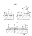
図3は、本発明の自発光平面表示装置を構成する表示パネルの実施例2を説明する模式図であり、背面パネルの内面構成を説明する図である。なお、実施例2の背面パネルの平面図は図1と同様である。図3(a)は図1(a)のA−A’線に沿った部分断面図、図3(b)は図1(a)のB−B’線に沿った部分断面図、図3(c)は図1(a)のC−C’線に沿った部分断面図である。実施例2における背面パネルと前面パネルは、両者の外周内縁に封止枠MFLを介在させ、接着剤としてフリットガラスFGで接着されて一体化されている。封止枠MFLでの封止領域を符号SLで示してある。 FIG. 3 is a schematic diagram for explaining Example 2 of the display panel constituting the self-luminous flat display device of the present invention, and is a diagram for explaining the inner surface configuration of the back panel. In addition, the top view of the back panel of Example 2 is the same as that of FIG. 3A is a partial cross-sectional view taken along line AA ′ in FIG. 1A, FIG. 3B is a partial cross-sectional view taken along line BB ′ in FIG. (C) is the fragmentary sectional view which followed CC 'line of Fig.1 (a). The back panel and the front panel in the second embodiment are integrated by being bonded with a frit glass FG as an adhesive with a sealing frame MFL interposed between the inner peripheral edges thereof. A sealing region in the sealing frame MFL is indicated by reference sign SL.
実施例1と同様に、背面パネルには、背面基板SUB1の上にカソード電極CLとゲート電極GLが形成されている。カソード電極CLの端部にはカソード電極引出端子CLT を有し、ゲート電極GLの端部にはゲート電極引出端子GLTを有する。カソード電極CLはストライプ状電極であり、背面基板SUB1上の第1の方向に延在して第1の方向と交差する第2の方向に多数並設されている。このカソード電極CLの上を覆って絶縁膜(層間絶縁膜)INSが形成されている。この絶縁膜INS上で上記第2の方向に延在して上記第1の方向に多数のゲート電極GLが並設されている。ゲート電極GLもストライプ状電極である。平面配置は図1(a)と同様である。 As in the first embodiment, the cathode electrode CL and the gate electrode GL are formed on the back substrate SUB1 on the back panel. A cathode electrode lead terminal CLT is provided at the end of the cathode electrode CL, and a gate electrode lead terminal GLT is provided at the end of the gate electrode GL. The cathode electrode CL is a stripe-like electrode, and extends in the first direction on the back substrate SUB1 and is arranged in parallel in a second direction intersecting the first direction. An insulating film (interlayer insulating film) INS is formed so as to cover the cathode electrode CL. On the insulating film INS, a large number of gate electrodes GL are arranged in parallel in the first direction so as to extend in the second direction. The gate electrode GL is also a striped electrode. The planar arrangement is the same as in FIG.
実施例2の表示領域におけるカソード電極CLとゲート電極GLの層構造を図3(a)に示す。なお、電子源は図示を省略してある。カソード電極CLは背面基板SUB1の上に形成され、その上を覆って層間絶縁膜INSが形成されている。実施例2では、層間絶縁膜INSとして窒化シリコン(SiN)を用いた。層間絶縁膜INSの上にゲート電極GLが形成されている。ゲート電極GLの端部はゲート電極引出端子GLTとなって封止領域SLの外側に引き出されている。 FIG. 3A shows the layer structure of the cathode electrode CL and the gate electrode GL in the display region of the second embodiment. The electron source is not shown. The cathode electrode CL is formed on the back substrate SUB1, and an interlayer insulating film INS is formed to cover the cathode electrode CL. In Example 2, silicon nitride (SiN) was used as the interlayer insulating film INS. A gate electrode GL is formed on the interlayer insulating film INS. An end portion of the gate electrode GL serves as a gate electrode lead terminal GLT and is drawn outside the sealing region SL.
層間絶縁膜INSは、図3(b)に示すように、封止領域SLではゲート電極引出端子GLTの下層にのみ有している。封止領域SLでは、封止枠MFLを接着する接着剤FGとはゲート電極引出端子GLTの下層の側面のみと接触している。実施例2では、接着剤FGとして酸化鉛(PbO)を含むフリットガラスを用いた。図3(c)に示すように、背面パネルを構成する背面基板SUB1と封止枠MFLの間にはゲート電極引出端子GLTとこのゲート電極引出端子GLTの下層に残された層間絶縁膜INS、および接着剤FGが介在することになる。 As shown in FIG. 3B, the interlayer insulating film INS is provided only under the gate electrode lead terminal GLT in the sealing region SL. In the sealing region SL, the adhesive FG that bonds the sealing frame MFL is in contact with only the side surface of the lower layer of the gate electrode lead terminal GLT. In Example 2, frit glass containing lead oxide (PbO) was used as the adhesive FG. As shown in FIG. 3 (c), between the back substrate SUB1 constituting the back panel and the sealing frame MFL, a gate electrode lead terminal GLT and an interlayer insulating film INS remaining under the gate electrode lead terminal GLT, In addition, the adhesive FG is interposed.
実施例2の構成としたことにより、前記したPbO+SiN→Pb+SiO2 +NOの反応は、ゲート電極引出端子GLTの下層の側面でのみ発生する可能性はあるが、この部分の接触面積は極めて小さいため、両者間に化学反応が生じても、それは僅かであり、真空リークの可能性は極めて小さい。そのため、信頼性の高い自発光平面表示装置を提供することができる。 With the configuration of Example 2, the above-described reaction of PbO + SiN → Pb + SiO 2 + NO may occur only on the side surface of the lower layer of the gate electrode lead terminal GLT, but the contact area of this part is extremely small. Even if a chemical reaction occurs between the two, it is very small and the possibility of a vacuum leak is extremely small. Therefore, a highly reliable self-luminous flat panel display can be provided.
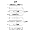
図4は、実施例2の背面パネルの製造方法を説明する図である。以下、製造工程順に説明する。先ず、背面基板の全面に、金属(アルミニウム等)の蒸着により第1電極膜を成膜する(p−11)。実施例2でも、第1電極はカソード電極であり、カソード電極引出端子ともなる。第1電極膜を覆って感光性レジストを塗布し、乾燥してカソード電極とカソード電極引出端子のパターンを有するホトマスクを用いて露光し、現像処理を施すホトリソグラフィー手法でパターニングを行い、カソード電極とカソード電極引出端子となる部分を除いて第1電極膜を露出させる(p−12)。 FIG. 4 is a diagram for explaining the manufacturing method of the back panel according to the second embodiment. Hereinafter, it demonstrates in order of a manufacturing process. First, a first electrode film is formed on the entire surface of the back substrate by vapor deposition of metal (aluminum or the like) (p-11). Also in Example 2, the first electrode is a cathode electrode and also serves as a cathode electrode lead-out terminal. A photosensitive resist is applied to cover the first electrode film, dried, exposed using a photomask having a cathode electrode and cathode electrode lead-out terminal pattern, and patterned by a photolithography technique for performing a development process. The first electrode film is exposed except for the portion serving as the cathode electrode lead terminal (p-12).
感光性レジストから露出した部分の第1電極膜をウエットエッチングにより溶解除去することでカソード電極とカソード電極引出端子を形成する(p−3)。なお、この後、残留した感光性レジストを剥離剤や水洗で除去し、洗浄する。 A portion of the first electrode film exposed from the photosensitive resist is dissolved and removed by wet etching to form a cathode electrode and a cathode electrode lead terminal (p-3). Thereafter, the remaining photosensitive resist is removed by a stripping agent or washing with water and washed.
形成したカソード電極とカソード電極引出端子の全面、かつ封止枠で封止される封止領域(シール領域)を超えて背面基板の端まで絶縁膜(層間絶縁膜となる)を形成する(p−14)。この絶縁膜としては、窒化シリコン(SiN)を用いる。 An insulating film (becomes an interlayer insulating film) is formed over the entire surface of the formed cathode electrode and cathode electrode lead-out terminal and beyond the sealing region (sealing region) sealed by the sealing frame to the end of the back substrate (p) -14). As this insulating film, silicon nitride (SiN) is used.
絶縁膜を形成した背面基板の全面(カソード電極とカソード電極引出端子と)を覆って金属(アルミニウム等)の蒸着で第2電極膜を形成する(p−15)。実施例2でも、第2電極はゲート電極であり、ゲート電極引出端子ともなる。 A second electrode film is formed by vapor deposition of metal (aluminum or the like) covering the entire surface (cathode electrode and cathode electrode lead terminal) of the rear substrate on which the insulating film is formed (p-15). Also in Example 2, the second electrode is a gate electrode and also serves as a gate electrode lead-out terminal.
形成した第2金属膜を覆って感光性レジストを塗布し、乾燥してゲート電極とゲート電極引出端子のパターンを有するホトマスクを用いて露光し、現像処理を施すホトリソグラフィー手法でパターニングを行い、ゲート電極とゲート電極引出端子となる部分を除いて第2電極膜を露出させる(p−16)。 A photosensitive resist is applied to cover the formed second metal film, dried, exposed using a photomask having a pattern of a gate electrode and a gate electrode lead-out terminal, and patterned by a photolithography technique in which development processing is performed. The second electrode film is exposed except for the portion that becomes the electrode and the gate electrode lead terminal (p-16).
感光性レジストから露出した部分の第2電極膜をウエットエッチングにより溶解除去することでゲート電極とゲート電極引出端子を形成する(p−17)。なお、この後、残留した感光性レジストを剥離剤や水洗で除去し、洗浄する。 A portion of the second electrode film exposed from the photosensitive resist is dissolved and removed by wet etching to form a gate electrode and a gate electrode lead terminal (p-17). Thereafter, the remaining photosensitive resist is removed by a stripping agent or washing with water and washed.
その後、封止枠で封止される封止領域(ゲート電極引出端子の間を含む)、電子源及び第1電極引出端子部の層間絶縁膜を除去する(p−18)。これにより、封止領域にはゲート電極引出端子の下層にのみ層間絶縁膜が存在する。こうして製造された背面パネルに封止枠を介して前面パネルを貼り合せ、真空抜きして自発光平面表示装置を構成する表示パネルが完成する。 Thereafter, the sealing region (including between the gate electrode lead terminals) sealed with the sealing frame, the interlayer insulating film of the electron source and the first electrode lead terminal part are removed (p-18). Thus, the interlayer insulating film exists only in the lower layer of the gate electrode lead terminal in the sealing region. The front panel is bonded to the rear panel thus manufactured through a sealing frame, and the vacuum is released to complete the display panel constituting the self-luminous flat display device.
図5は、本発明の自発光平面表示装置を構成する表示パネルの実施例3を説明する要部模式図であり、背面パネルのゲート電極引出端子と封止領域の部分の平面図である。実施例3は実施例2の構造を基本とし、封止領域SLにおけるゲート電極引出端子GLTの一方の側縁の長さを、該ゲート電極引出端子GLTの封止領域における引き出し距離よりも長い平面形状を有するものとした。下層に介在する層間絶縁膜は該ゲート電極引出端子GLTの平面形状に倣って存在する。 FIG. 5 is a schematic view of the main part for explaining a third embodiment of the display panel constituting the self-luminous flat display device of the present invention, and is a plan view of the gate electrode lead-out terminal and the sealing region portion of the back panel. The third embodiment is based on the structure of the second embodiment, and the length of one side edge of the gate electrode lead terminal GLT in the sealing region SL is longer than the lead distance in the sealing region of the gate electrode lead terminal GLT. It had a shape. The interlayer insulating film interposed in the lower layer is present following the planar shape of the gate electrode lead terminal GLT.
図5では、封止領域SLにおける第2電極引出端子GLTの側縁に突起Pを設けた。これにより、封止領域SLにおける第2電極引出端子GLTの側縁の長さL1(第2電極引出端子GLTの下層にある層間絶縁膜INSの長さも同じ)は該封止領域SLにおける第2電極引出端子GLTの引き出し長さL2より長くなる。そのため、この層間絶縁膜INSと封止枠FMLを背面パネルに接着する接着剤との接触距離も同様に長くなる。その結果、真空リークの可能性を低減できる。 In FIG. 5, the protrusion P is provided on the side edge of the second electrode lead terminal GLT in the sealing region SL. Thereby, the length L1 of the side edge of the second electrode lead terminal GLT in the sealing region SL (the length of the interlayer insulating film INS under the second electrode lead terminal GLT is also the same) is the second length in the sealing region SL. It becomes longer than the lead length L2 of the electrode lead terminal GLT. Therefore, the contact distance between the interlayer insulating film INS and the adhesive that bonds the sealing frame FML to the back panel is also increased. As a result, the possibility of vacuum leakage can be reduced.
なお、封止領域SLにおける第2電極引出端子GLTの側縁の長さL1を該封止領域SLにおける第2電極引出端子GLTの引き出し長さL2より長くするための電極形状は、図5に示したものに限らず、他の適当な形状、例えば屈曲形、蛇行形、その他の不定形等とすることができる。また、この電極形状はゲート電極引出端子に限らず、カソード電極引出端子にも適用できる。 The electrode shape for making the length L1 of the side edge of the second electrode lead terminal GLT in the sealing region SL longer than the lead length L2 of the second electrode lead terminal GLT in the sealing region SL is shown in FIG. The present invention is not limited to those shown, and other suitable shapes such as a bent shape, a meandering shape, and other indefinite shapes can be used. Moreover, this electrode shape is applicable not only to a gate electrode lead terminal but also to a cathode electrode lead terminal.
図6は、本発明による自発光平面表示装置の全体構造の一例を説明する一部破断して示す斜視図である。また、図7は、図6のA−A’線に沿って切断した断面図である。背面パネルを構成する背面基板SUB1の内面にはカソード電極CLとゲート電極GLを有し、カソード電極CLとゲート電極GLの交差部分に電子源が形成されている。カソード電極CLの端部にはカソード電極引出線CLTが形成され、ゲート電極GLの端部にはゲート電極引出線GLTが形成されている。 FIG. 6 is a partially broken perspective view illustrating an example of the entire structure of the self-luminous flat panel display device according to the present invention. FIG. 7 is a cross-sectional view taken along the line A-A ′ of FIG. 6. The inner surface of the rear substrate SUB1 constituting the rear panel has a cathode electrode CL and a gate electrode GL, and an electron source is formed at the intersection of the cathode electrode CL and the gate electrode GL. A cathode electrode lead line CLT is formed at the end of the cathode electrode CL, and a gate electrode lead line GLT is formed at the end of the gate electrode GL.
前面パネルを構成する前面基板SUB2の内面には陽極ADと蛍光体層PHが形成されている。背面パネルPNL1を構成する背面基板SUB1と前面パネルPNL2を構成する前面基板SUB2とは、その周縁に封止枠MFLを介在させて貼り合わされる。この貼り合わせた間隙を所定値に保持するため、背面パネルSUB1と前面パネルPNL2の間にガラス板を好適とする隔壁SPCを植立させている。図7はこの隔壁SPCに沿った断面なので、隔壁SPCは図示を省略してある。 An anode AD and a phosphor layer PH are formed on the inner surface of the front substrate SUB2 constituting the front panel. The rear substrate SUB1 constituting the rear panel PNL1 and the front substrate SUB2 constituting the front panel PNL2 are bonded together with a sealing frame MFL interposed therebetween. In order to maintain the bonded gap at a predetermined value, a partition wall SPC having a glass plate is planted between the rear panel SUB1 and the front panel PNL2. Since FIG. 7 is a cross section along the partition wall SPC, the partition wall SPC is not shown.
なお、背面パネルPNL1と前面パネルPNL2および封止枠MFLで密封された内部空間は、背面パネルPNL1の一部に設けた排気管EXCから排気して所定の真空状態にする。 The internal space sealed by the back panel PNL1, the front panel PNL2, and the sealing frame MFL is exhausted from an exhaust pipe EXC provided in a part of the back panel PNL1, and is brought into a predetermined vacuum state.
図8は、本発明の自発光平面表示装置の画素を構成する電子源の一例を説明する図であり、図8(a)は平面図、図8(b)は図8(a)のA−A'線に沿う断面図、図8(c)は図8(a)のB−B'線に沿う断面図である。この電子源はMIM電子源である。 8A and 8B are diagrams for explaining an example of an electron source that constitutes a pixel of the self-luminous flat display device of the present invention. FIG. 8A is a plan view, and FIG. 8B is A in FIG. FIG. 8C is a cross-sectional view taken along the line BB ′ in FIG. 8A. This electron source is a MIM electron source.
この電子源の構造を、その製造工程で説明する。先ず、背面基板SUB1上に下部電極DED(前記の各実施例におけるカソード電極CL)、保護絶縁層INS1、絶縁層INS2を形成する。次に、層間膜INS3と、上部電極AEDへの給電線となる上部バス電極AED(前記の各実施例におけるゲート電極GL)とスペーサを配置するためのスペーサ電極となる金属膜を、例えばスパッタリング法等で成膜する。下部電極や上部電極にはアルミニウムを用いることができるが、後述する他の金属も用いることができる。 The structure of this electron source will be described in the manufacturing process. First, the lower electrode DED (the cathode electrode CL in each of the above embodiments), the protective insulating layer INS1, and the insulating layer INS2 are formed on the back substrate SUB1. Next, an interlayer film INS3, an upper bus electrode AED (gate electrode GL in each of the above-described embodiments) serving as a power supply line to the upper electrode AED, and a metal film serving as a spacer electrode for arranging the spacer are formed by, for example, sputtering. Etc. are formed. Aluminum can be used for the lower electrode and the upper electrode, but other metals described later can also be used.
層間膜INS3としては、例えばシリコン酸化物やシリコン窒化膜、シリコンなどを用いることができる。ここでは、シリコン窒化膜を用い膜厚は100nmとした。この層間膜INS3は、陽極酸化で形成する保護絶縁層INS1にピンホールがあった場合、その欠陥を埋め、下部電極DEDと走査信号配線となる上部バス電極(金属膜下層MDLと金属膜上層MALの間に金属膜中間層MMLとしてCuを挟んだ3層の積層膜)間の絶縁を保つ役割を果たす。 As the interlayer film INS3, for example, silicon oxide, silicon nitride film, silicon, or the like can be used. Here, a silicon nitride film is used and the film thickness is 100 nm. When the protective insulating layer INS1 formed by anodic oxidation has a pinhole, the interlayer film INS3 fills the defect, and forms an upper bus electrode (metal film lower layer MDL and metal film upper layer MAL serving as a scanning signal wiring) The metal film intermediate layer MML has a role of maintaining insulation between the three laminated films sandwiching Cu.
なお、上部バス電極AEDは、上記の3層積層膜は限らず、それ以上とすることもできる。例えば、金属膜下層MDL、金属膜上層MALとしてAlやクロム(Cr)、タングステン(W)、モリブデン(Mo)などの耐酸化性の高い金属材料、またはそれらを含む合金やそれらの積層膜を用いることができる。なお、ここでは金属膜下層MDL、金属膜上層MALとしてAl−Nd合金を用いた。この他に、金属膜下層MDLとしてAl合金とCr、W、Moなどの積層膜を用い、金属膜上層MALとしてCr、W、MoなどとAl合金の積層膜を用いて、金属膜中間層MMLのCuに接する膜を高融点金属とした5層膜を用いることで、画像表示装置の製造プロセスにおける加熱工程の際に、高融点金属がバリア膜となってAlとCuの合金化を抑制できるので、低抵抗化に特に有効である。 Note that the upper bus electrode AED is not limited to the above three-layer laminated film, and may be more than that. For example, as the metal film lower layer MDL and the metal film upper layer MAL, a metal material having high oxidation resistance such as Al, chromium (Cr), tungsten (W), molybdenum (Mo), an alloy containing them, or a laminated film thereof is used. be able to. Here, an Al—Nd alloy was used as the metal film lower layer MDL and the metal film upper layer MAL. In addition, a metal film intermediate layer MML is formed by using an Al alloy and a laminated film of Cr, W, Mo, etc. as the metal film lower layer MDL and using a laminated film of Cr, W, Mo, etc. and an Al alloy as the metal film upper layer MAL. By using a five-layer film in which the film in contact with Cu is a refractory metal, the refractory metal becomes a barrier film during the heating process in the manufacturing process of the image display device, and alloying of Al and Cu can be suppressed. Therefore, it is particularly effective for reducing the resistance.
Al−Nd合金のみ用いる場合の、当該Al−Nd合金の膜厚は、金属膜下層MDLより金属膜上層MALを厚くし、金属膜中間層MMLのCuは配線抵抗を低減するため、できるだけ厚くしておく。ここでは金属膜下層MDLを300nm、金属膜中間層MMLを4μm、金属膜上層MALを450nmの膜厚とした。なお、金属膜中間層MMLのCuはスパッタ以外に電気めっきなどにより形成することも可能である。 When only the Al—Nd alloy is used, the film thickness of the Al—Nd alloy is made as thick as possible in order to make the metal film upper layer MAL thicker than the metal film lower layer MDL and to reduce the wiring resistance of the metal film intermediate layer MML. Keep it. Here, the metal film lower layer MDL is 300 nm, the metal film intermediate layer MML is 4 μm, and the metal film upper layer MAL is 450 nm. Note that Cu in the metal film intermediate layer MML can be formed by electroplating or the like in addition to sputtering.
高融点金属を用いる上記5層膜の場合は、Cuと同様に、特に燐酸、酢酸、硝酸の混合水溶液でのウェットエッチングが可能なMoでCuを挟んだ積層膜を金属膜中間層MMLとして用いるのが特に有効である。この場合、Cuを挟むMoの膜厚は50nmとし、この金属膜中間層を挟む金属膜下層MDLのAl合金は300nm、金属膜上層MALのAl合金は50nmの膜厚とする。 In the case of the above-mentioned five-layer film using a refractory metal, a multilayer film in which Cu is sandwiched between Mo that can be wet-etched with a mixed aqueous solution of phosphoric acid, acetic acid and nitric acid is used as the metal film intermediate layer MML. Is particularly effective. In this case, the film thickness of Mo sandwiching Cu is 50 nm, the Al alloy of the metal film lower layer MDL sandwiching the metal film intermediate layer is 300 nm, and the Al alloy of the metal film upper layer MAL is 50 nm.
続いて、スクリーン印刷によるレジストのパターニングとエッチング加工により金属膜上層MALを、下部電極DEDと交差するストライプ形状に加工する。このエッチング加工では、例えば燐酸、酢酸の混合水溶液でのウェットエッチングを用いる。エッチング液に硝酸を加えないことによりCuをエッチングせずにAl−Nd合金のみを選択的にエッチングすることが可能となる。 Subsequently, the metal film upper layer MAL is processed into a stripe shape intersecting with the lower electrode DED by patterning a resist by screen printing and etching. In this etching process, for example, wet etching using a mixed aqueous solution of phosphoric acid and acetic acid is used. By not adding nitric acid to the etching solution, it is possible to selectively etch only the Al—Nd alloy without etching Cu.
Moを用いた5層膜の場合も、エッチング液に硝酸を加えないことによりMoとCuをエッチングせずに、Al−Nd合金のみのみ選択的にエッチング加工することが可能である。ここでは、金属膜上層MALを1画素あたり1本形成したが、2本形成することも可能である。 Even in the case of a five-layer film using Mo, it is possible to selectively etch only the Al—Nd alloy without etching Mo and Cu by not adding nitric acid to the etching solution. Although one metal film upper layer MAL is formed per pixel here, two metal film upper layers MAL may be formed.
続いて、同じレジスト膜をそのまま用いるか、金属膜上層MALのAl−Nd合金をマスクとして金属膜中間層MMLのCuを例えば燐酸、酢酸、硝酸の混合水溶液でウェットエッチングする。燐酸、酢酸、硝酸の混合水溶液のエッチング液中でのCuのエッチング速度はAl−Nd合金に比べて十分に速いため、金属膜中間層MMLのCuのみを選択的にエッチングすることが可能である。Moを用いた5層膜の場合もMoとCuのエッチング速度はAl−Nd合金に比べて十分に速くMoとCuの3層の積層膜のみを選択的にエッチングすることが可能である。Cuのエッチングにはその他過硫酸アンモニウム水溶液や過硫酸ナトリウム水溶液も有効である。 Subsequently, the same resist film is used as it is, or Cu of the metal film intermediate layer MML is wet-etched with a mixed aqueous solution of phosphoric acid, acetic acid and nitric acid, for example, using the Al—Nd alloy of the metal film upper layer MAL as a mask. Since the etching rate of Cu in an etching solution of a mixed aqueous solution of phosphoric acid, acetic acid, and nitric acid is sufficiently higher than that of an Al—Nd alloy, only Cu in the metal film intermediate layer MML can be selectively etched. . Even in the case of a five-layer film using Mo, the etching rate of Mo and Cu is sufficiently higher than that of an Al—Nd alloy, and it is possible to selectively etch only the three-layered film of Mo and Cu. Other ammonium persulfate aqueous solutions and sodium persulfate aqueous solutions are also effective for etching Cu.
続いて、スクリーン印刷によるレジストのパターニングとエッチング加工により金属膜下層MDLを下部電極DEDと交差するストライプ形状に加工する。このエッチング加工は燐酸、酢酸の混合水溶液でのウェットエッチングで行う。その際、印刷するレジスト膜を金属膜上層MALのストライプ電極とは平行な方向に位置をずらすことにより、金属膜下層MDLの片側EG1は金属膜上層MALより張り出させて、後の工程で上部電極AEDとの接続を確保するコンタクト部とし、金属膜下層MDLの反対側EG2では金属膜上層MALと金属膜中間層MLをマスクとしてオーバーエッチング加工がなされ、金属膜中間層MMLに庇を形成する如く後退した部分が形成される。 Subsequently, the metal film lower layer MDL is processed into a stripe shape intersecting with the lower electrode DED by resist patterning and etching by screen printing. This etching process is performed by wet etching with a mixed aqueous solution of phosphoric acid and acetic acid. At that time, by shifting the position of the resist film to be printed in a direction parallel to the stripe electrode of the metal film upper layer MAL, one side EG1 of the metal film lower layer MDL protrudes from the metal film upper layer MAL, As a contact portion that secures connection with the electrode AED, overetching is performed on the opposite side EG2 of the metal film lower layer MDL using the metal film upper layer MAL and the metal film intermediate layer ML as a mask to form a ridge in the metal film intermediate layer MML Thus, a receding part is formed.
この金属膜中間層MMLの庇により、後の工程で成膜される上部電極AEDが分離される。この際、金属膜上層MALは金属膜下層MDLの膜厚より厚くしてあるので、金属膜下層MDLのエッチングが終了しても、金属膜上層MALは金属膜中間層MMLのCu上に残すことができる。これによりCuの表面を保護することが可能となるので、Cuを用いても耐酸化性があり、かつ上部電極AEDを自己整合的に分離し、かつ給電を行う走査信号配線となる上部バス電極を形成することができる。また、CuをMoで挟んだ5層膜の金属膜中間層MMLとした場合には、金属膜上層MALのAl合金が薄くても、MoがCuの酸化を抑制してくれるので、金属膜上層MALを金属膜下層MDLの膜厚より厚くする必要は必ずしもない。 The upper electrode AED formed in a later step is separated by the metal film intermediate layer MML. At this time, since the metal film upper layer MAL is thicker than the film thickness of the metal film lower layer MDL, even if the etching of the metal film lower layer MDL is finished, the metal film upper layer MAL remains on the Cu of the metal film intermediate layer MML. Can do. As a result, the surface of Cu can be protected, so that the upper bus electrode which is oxidation resistant even if Cu is used, and which separates the upper electrode AED in a self-aligned manner and serves as a scanning signal wiring for supplying power Can be formed. Further, in the case of a five-layer metal film intermediate layer MML in which Cu is sandwiched between Mo, even if the Al alloy of the metal film upper layer MAL is thin, Mo suppresses oxidation of Cu, so the metal film upper layer It is not always necessary to make MAL thicker than the film thickness of the metal film lower layer MDL.
続いて、層間膜INS3を加工して電子放出部を開口する。電子放出部は画素内の1本の下部電極DEDと、下部電極DEDと交差する2本の上部バス電極(金属膜下層MDL、金属膜中間層MML、金属膜上層MALの積層膜と非図示の隣接画素の金属膜下層MDL、金属膜中間層MML、金属膜上層MALの積層膜)に挟まれた空間の交差部の一部に形成する。このエッチング加工は、例えばCF4やSF6を主成分とするエッチングガスを用いたドライエッチングによって行うことができる。 Subsequently, the interlayer film INS3 is processed to open an electron emission portion. The electron emission portion includes one lower electrode DED in the pixel and two upper bus electrodes (a metal film lower layer MDL, a metal film intermediate layer MML, and a metal film upper layer MAL laminated film and a non-illustrated film) intersecting the lower electrode DED. It is formed in a part of the intersection of the space sandwiched between the metal film lower layer MDL, the metal film intermediate layer MML, and the metal film upper layer MAL of the adjacent pixel. This etching process can be performed, for example, by dry etching using an etching gas containing CF 4 or SF 6 as a main component.
最後に、上部電極AEDの成膜を行う。この成膜にはスパッタ法を用いる。上部電極AEDとしては、アルミニウムでも良く、あるいはIr、Pt、Auの積層膜を用い、その膜厚は例えば6nmとすることもできる。この時、上部電極AEDは、電子放出部を挟む2本の上部バス電極(金属膜下層MDL、金属膜中間層MML、金属膜上層MALの積層膜)の一方(図8(c)の右側)では、金属膜中間層MMLと金属膜上層MALの庇構造による金属膜下層MDLの後退部(EG2)により切断される。そして、他方(図8(c)の左側)では、上部バス電極(金属膜下層MDL、金属膜中間層MML、金属膜上層MALの積層膜)とは金属膜下層MDLのコンタクト部(EG1)により断線を起こさずに成膜接続されて、電子放出部への給電される構造となる。 Finally, the upper electrode AED is formed. A sputtering method is used for this film formation. As the upper electrode AED, aluminum may be used, or a laminated film of Ir, Pt, and Au may be used, and the film thickness may be 6 nm, for example. At this time, the upper electrode AED is one of the two upper bus electrodes (a laminated film of the metal film lower layer MDL, the metal film intermediate layer MML, and the metal film upper layer MAL) sandwiching the electron emission portion (right side of FIG. 8C). In this case, the metal film intermediate layer MML and the metal film upper layer MAL are cut by the receding portion (EG2) of the metal film lower layer MDL having a saddle structure. On the other hand (on the left side of FIG. 8C), the upper bus electrode (laminated film of the metal film lower layer MDL, the metal film intermediate layer MML, and the metal film upper layer MAL) is separated from the contact portion (EG1) of the metal film lower layer MDL. The structure is such that the film is connected without causing disconnection and power is supplied to the electron emission portion.
図9は、本発明の構成を適用した画像表示装置の等価回路例の説明図である。図9中に破線で示した領域は表示領域ARであり、この表示領域ARにn本のカソード電極CLとm本のゲート電極GLが互いに交差して配置されてn×mのマトリクスが形成されている。マトリクスの各交差部は副画素を構成し、図中の3つの単位画素(あるいは、副画素)"R","G","B"の1グループでカラー1画素を構成する。なお、電子源の構成は図示を省いた。カソード電極CLは、カソード電極引出端子CLTで画像信号駆動回路DDRに接続され、ゲート電極GLはゲート電極引出端子GLTで走査信号駆動回路SDRに接続されている。画像信号駆動回路DDRには外部信号源から画像信号NSが入力され、走査信号駆動回路SDRには同様に走査信号SSが入力される。 FIG. 9 is an explanatory diagram of an example of an equivalent circuit of an image display device to which the configuration of the present invention is applied. A region indicated by a broken line in FIG. 9 is a display region AR. In this display region AR, n cathode electrodes CL and m gate electrodes GL are arranged so as to cross each other to form an n × m matrix. ing. Each intersection of the matrix constitutes a sub-pixel, and one group of three unit pixels (or sub-pixels) “R”, “G”, and “B” in the figure constitutes one color pixel. The configuration of the electron source is not shown. The cathode electrode CL is connected to the image signal drive circuit DDR at the cathode electrode lead-out terminal CLT, and the gate electrode GL is connected to the scanning signal drive circuit SDR at the gate electrode lead-out terminal GLT. The image signal NS is input from the external signal source to the image signal driving circuit DDR, and the scanning signal SS is similarly input to the scanning signal driving circuit SDR.
これにより、順次選択されるゲート電極GLに交差するカソード電極CLに画像信号を供給することで、二次元のフルカラー画像を表示することができる。本構成例の表示パネルを用いることにより、比較的低電圧で高効率の自発光平面表示装置が実現される。 Accordingly, a two-dimensional full-color image can be displayed by supplying an image signal to the cathode electrode CL that intersects the gate electrode GL that is sequentially selected. By using the display panel of this configuration example, a self-luminous flat display device with relatively low voltage and high efficiency is realized.
PNL1・・・背面パネル、PNL2・・・前面パネル、SUB1・・・背面基板、SUB2・・・前面基板、CL・・・カソード電極、CLT・・・カソード電極引出端子、GL・・・ゲート電極、GLT・・・ゲート電極引出端子、PH・・・蛍光体層、AD・・・陽極、INS・・・絶縁膜(層間絶縁膜)、MFL・・・封止枠、FG・・・フリットガラス。
PNL1 ... back panel, PNL2 ... front panel, SUB1 ... back substrate, SUB2 ... front substrate, CL ... cathode electrode, CLT ... cathode electrode lead terminal, GL ... gate electrode , GLT: gate electrode lead terminal, PH: phosphor layer, AD ... anode, INS ... insulating film (interlayer insulating film), MFL ... sealing frame, FG ... frit glass .
Claims (15)
前記背面パネルの前記表示領域に有する前記電子源から取り出される電子の励起で発光する複数色の蛍光体層と第3電極を前面基板に形成した前面パネルと、
前記背面パネルと前記前面パネルの周辺部に介在して両パネルを封止する封止枠とを具備し、
前記第1電極の少なくとも一端は前記表示領域から前記背面パネルと前記封止枠とが対向する封止領域を通して外側に引き出された第1電極引出端子を有し、
前記第2電極の少なくとも一端は前記表示領域から前記背面パネルと前記封止枠とが対向する封止領域を通して外側に引き出された第2電極引出端子を有し、
前記絶縁膜は、前記封止枠による封止領域を除いて形成されている表示パネルを具備したことを特徴とする自発光平面表示装置。 A plurality of first electrodes extending in a first direction and arranged in parallel in a second direction intersecting the first direction, an insulating film formed to cover the first electrode, and the insulating film A plurality of second electrodes extending in the second direction and arranged in parallel in the first direction, and an electron source provided in the vicinity of the intersection of the first electrode and the second electrode. A back panel in which a display area having a large number of pixels is formed on a back substrate;
A front panel in which a plurality of color phosphor layers that emit light by excitation of electrons extracted from the electron source in the display area of the back panel and a third electrode are formed on a front substrate;
Comprising a sealing frame that seals both the back panel and the front panel interposed between the front panel,
At least one end of the first electrode has a first electrode lead terminal drawn out from the display region through a sealing region where the back panel and the sealing frame face each other,
At least one end of the second electrode has a second electrode lead terminal that is led out from the display region through a sealing region where the back panel and the sealing frame are opposed to each other,
The self-luminous flat panel display device, wherein the insulating film includes a display panel formed excluding a sealing region by the sealing frame.
前記背面パネルの前記表示領域に有する前記電子源から取り出される電子の励起で発光する複数色の蛍光体層と第3電極を前面基板に形成した前面パネルと、
前記背面パネルと前記前面パネルの周辺部に介在して両パネルを封止する封止枠とを具備し、
前記第1電極の少なくとも一端は前記表示領域から前記背面パネルと前記封止枠とが対向する封止領域を通して外側に引き出された第1電極引出端子を有し、
前記第2電極の少なくとも一端は前記表示領域から前記背面パネルと前記封止枠とが対向する封止領域を通して外側に引き出された第2電極引出端子を有し、
前記絶縁膜は、前記封止枠による封止領域では前記第2電極引出端子の間を除いて形成されている表示パネルを具備したことを特徴とする自発光平面表示装置。 A plurality of first electrodes extending in a first direction and arranged in parallel in a second direction intersecting the first direction, an insulating film formed to cover the first electrode, and the insulating film A plurality of second electrodes extending in the second direction and arranged in parallel in the first direction, and an electron source provided in the vicinity of the intersection of the first electrode and the second electrode. A back panel in which a display area having a large number of pixels is formed on a back substrate;
A front panel in which a plurality of color phosphor layers that emit light by excitation of electrons extracted from the electron source in the display area of the back panel and a third electrode are formed on a front substrate;
Comprising a sealing frame that seals both the back panel and the front panel interposed between the front panel,
At least one end of the first electrode has a first electrode lead terminal drawn out from the display region through a sealing region where the back panel and the sealing frame face each other,
At least one end of the second electrode has a second electrode lead terminal that is led out from the display region through a sealing region where the back panel and the sealing frame are opposed to each other,
The self-luminous flat panel display according to claim 1, wherein the insulating film includes a display panel formed in a sealing region by the sealing frame except between the second electrode lead terminals.
前記背面パネルを構成する絶縁基板の全面に第1電極および第1電極引出端子を形成するための第1金属膜を形成する第1金属膜形成工程と、
形成した前記第1金属膜の上に感光性レジストを塗布し、前記第1電極および第1電極引出端子のパターンを露光と現像処理により前記第1金属膜に露出部分を形成するパターニング工程と、
前記第1金属膜の露出部分をエッチング加工し、加工後に前記感光性レジストを除去して第1電極および第1電極引出端子を形成するエッチング処理工程と、
前記第1電極の全面を覆い、かつ前記封止枠で封止される封止領域の内側まで絶縁膜を形成する絶縁膜形成工程と、
前記第1電極と前記絶縁膜を覆って前記絶縁基板の全面に第2電極および第2電極引出端子を形成するための第2金属膜を形成する第2金属膜形成工程と、
形成した前記第2金属膜の上に感光性レジストを塗布し、前記第2電極および第2電極引出端子のパターンを露光と現像処理により前記第2金属膜に露出部分を形成するパターニング工程と、
前記第2金属膜の露出部分をエッチング加工し、加工後に前記感光性レジストを除去して第2電極および第2電極引出端子を形成するエッチング処理工程と、
前記封止枠で封止される封止領域の前記絶縁膜を除去する絶縁膜除去工程と、
を少なくとも含むことを特徴とする自発光平面表示装置の製造方法。 A method for manufacturing a self-luminous flat panel display device comprising a display panel formed by sealing a back panel and a front panel with a sealing frame,
A first metal film forming step of forming a first metal film for forming the first electrode and the first electrode lead terminal on the entire surface of the insulating substrate constituting the back panel;
Applying a photosensitive resist on the formed first metal film, and patterning the first electrode and the first electrode lead terminal to form an exposed portion on the first metal film by exposing and developing; and
An etching process step of etching the exposed portion of the first metal film, removing the photosensitive resist after the processing to form a first electrode and a first electrode lead terminal;
An insulating film forming step for covering the entire surface of the first electrode and forming an insulating film up to the inside of the sealing region sealed by the sealing frame;
A second metal film forming step of forming a second metal film for covering the first electrode and the insulating film and forming a second electrode and a second electrode lead terminal on the entire surface of the insulating substrate;
Applying a photosensitive resist on the formed second metal film, and patterning the second electrode and the second electrode lead terminal by exposing and developing to form an exposed portion on the second metal film; and
An etching process step of etching the exposed portion of the second metal film, removing the photosensitive resist after processing to form a second electrode and a second electrode lead terminal;
An insulating film removing step of removing the insulating film in the sealing region sealed with the sealing frame;
A self-luminous flat panel display manufacturing method comprising:
前記背面パネルを構成する絶縁基板の全面に第1電極および第1電極引出端子を形成するための第1金属膜を形成する第1金属膜形成工程と、
形成した前記第1金属膜の上に感光性レジストを塗布し、前記第1電極および第1電極引出端子のパターンを露光と現像処理により前記第1金属膜に露出部分を形成するパターニング工程と、
前記第1金属膜の露出部分をエッチング加工し、加工後に前記感光性レジストを除去して第1電極および第1電極引出端子を形成するエッチング処理工程と、
前記第1電極および第1電極引出端子の全面を覆い、かつ前記封止枠で封止される封止領域の外側まで絶縁膜を形成する絶縁形成工程と、
前記第1電極および第1電極引出端子と前記絶縁膜を覆って前記絶縁基板の全面に第2電極および第2電極引出端子を形成するための第2金属膜を形成する第2金属膜形成工程と、
形成した前記第2金属膜の上に感光性レジストを塗布し、前記第2電極および第2電極引出端子のパターンを露光と現像処理により前記第2金属膜に露出部分を形成するパターニング工程と、
前記第2金属膜の露出部分をエッチング加工し、加工後に前記感光性レジストを除去して第2電極および第2電極引出端子を形成するエッチング処理工程と、
前記封止枠で封止される封止領域の前記第2電極引出端子の間の前記絶縁膜を除去する絶縁膜除去工程と、
を少なくとも含むことを特徴とする自発光平面表示装置の製造方法。 A method for manufacturing a self-luminous flat panel display device comprising a display panel formed by sealing a back panel and a front panel with a sealing frame,
A first metal film forming step of forming a first metal film for forming the first electrode and the first electrode lead terminal on the entire surface of the insulating substrate constituting the back panel;
A patterning step of applying a photosensitive resist on the formed first metal film, and forming an exposed portion of the first electrode and the first electrode lead terminal on the first metal film by exposure and development;
An etching process step of etching the exposed portion of the first metal film, removing the photosensitive resist after the processing to form a first electrode and a first electrode lead terminal;
An insulation forming step of covering the entire surface of the first electrode and the first electrode lead terminal and forming an insulating film to the outside of the sealing region sealed by the sealing frame;
A second metal film forming step of forming a second metal film for covering the first electrode and the first electrode lead terminal and the insulating film to form the second electrode and the second electrode lead terminal on the entire surface of the insulating substrate; When,
A patterning step of applying a photosensitive resist on the formed second metal film, and exposing the pattern of the second electrode and the second electrode lead terminal to the second metal film by exposure and development;
An etching process step of etching the exposed portion of the second metal film, removing the photosensitive resist after processing to form a second electrode and a second electrode lead terminal;
An insulating film removing step for removing the insulating film between the second electrode lead terminals of the sealing region sealed with the sealing frame;
A self-luminous flat panel display manufacturing method comprising:
14. The method of manufacturing a self-luminous flat panel display according to claim 13, wherein the insulating film is removed by dry etching.
Priority Applications (3)
| Application Number | Priority Date | Filing Date | Title |
|---|---|---|---|
| JP2004246814A JP2006066199A (en) | 2004-08-26 | 2004-08-26 | Self-emitting flat panel display device and its manufacturing method |
| US11/207,135 US20060043876A1 (en) | 2004-08-26 | 2005-08-18 | Self-luminous planar display device and manufacturing method thereof |
| CN200510093502.4A CN1741234A (en) | 2004-08-26 | 2005-08-26 | Self-luminous planar display device and manufacturing method thereof |
Applications Claiming Priority (1)
| Application Number | Priority Date | Filing Date | Title |
|---|---|---|---|
| JP2004246814A JP2006066199A (en) | 2004-08-26 | 2004-08-26 | Self-emitting flat panel display device and its manufacturing method |
Publications (2)
| Publication Number | Publication Date |
|---|---|
| JP2006066199A true JP2006066199A (en) | 2006-03-09 |
| JP2006066199A5 JP2006066199A5 (en) | 2007-10-04 |
Family
ID=35942118
Family Applications (1)
| Application Number | Title | Priority Date | Filing Date |
|---|---|---|---|
| JP2004246814A Pending JP2006066199A (en) | 2004-08-26 | 2004-08-26 | Self-emitting flat panel display device and its manufacturing method |
Country Status (3)
| Country | Link |
|---|---|
| US (1) | US20060043876A1 (en) |
| JP (1) | JP2006066199A (en) |
| CN (1) | CN1741234A (en) |
Cited By (1)
| Publication number | Priority date | Publication date | Assignee | Title |
|---|---|---|---|---|
| JP2009301875A (en) * | 2008-06-13 | 2009-12-24 | Nippon Electric Glass Co Ltd | Supporting frame forming material |
Families Citing this family (2)
| Publication number | Priority date | Publication date | Assignee | Title |
|---|---|---|---|---|
| JP2007257840A (en) * | 2006-03-20 | 2007-10-04 | Hitachi Displays Ltd | Image display device |
| JP2009076206A (en) * | 2007-06-25 | 2009-04-09 | Hitachi Displays Ltd | Image display device and manufacturing method thereof |
Citations (6)
| Publication number | Priority date | Publication date | Assignee | Title |
|---|---|---|---|---|
| JPH0620590A (en) * | 1992-06-30 | 1994-01-28 | Canon Inc | Electron emission element, light emission element and image display |
| JPH09277586A (en) * | 1996-04-08 | 1997-10-28 | Canon Inc | Electron source, image forming device and manufacture thereof |
| JPH10188854A (en) * | 1996-12-26 | 1998-07-21 | Canon Inc | Image forming device and manufacture thereof |
| JP2000082382A (en) * | 1998-09-04 | 2000-03-21 | Canon Inc | Electron emitting element, electron source using it, and image forming device |
| JP2002352696A (en) * | 2001-05-23 | 2002-12-06 | Hitachi Ltd | Image display device |
| JP2004207090A (en) * | 2002-12-26 | 2004-07-22 | Hitachi Ltd | Picture display device |
-
2004
- 2004-08-26 JP JP2004246814A patent/JP2006066199A/en active Pending
-
2005
- 2005-08-18 US US11/207,135 patent/US20060043876A1/en not_active Abandoned
- 2005-08-26 CN CN200510093502.4A patent/CN1741234A/en active Pending
Patent Citations (6)
| Publication number | Priority date | Publication date | Assignee | Title |
|---|---|---|---|---|
| JPH0620590A (en) * | 1992-06-30 | 1994-01-28 | Canon Inc | Electron emission element, light emission element and image display |
| JPH09277586A (en) * | 1996-04-08 | 1997-10-28 | Canon Inc | Electron source, image forming device and manufacture thereof |
| JPH10188854A (en) * | 1996-12-26 | 1998-07-21 | Canon Inc | Image forming device and manufacture thereof |
| JP2000082382A (en) * | 1998-09-04 | 2000-03-21 | Canon Inc | Electron emitting element, electron source using it, and image forming device |
| JP2002352696A (en) * | 2001-05-23 | 2002-12-06 | Hitachi Ltd | Image display device |
| JP2004207090A (en) * | 2002-12-26 | 2004-07-22 | Hitachi Ltd | Picture display device |
Cited By (1)
| Publication number | Priority date | Publication date | Assignee | Title |
|---|---|---|---|---|
| JP2009301875A (en) * | 2008-06-13 | 2009-12-24 | Nippon Electric Glass Co Ltd | Supporting frame forming material |
Also Published As
| Publication number | Publication date |
|---|---|
| CN1741234A (en) | 2006-03-01 |
| US20060043876A1 (en) | 2006-03-02 |
Similar Documents
| Publication | Publication Date | Title |
|---|---|---|
| JP2004363075A (en) | Image display unit | |
| JP2006252979A (en) | Image display device | |
| US20080238293A1 (en) | Self-Luminous Planar Display Device | |
| JP2006066199A (en) | Self-emitting flat panel display device and its manufacturing method | |
| JP2007123155A (en) | Image display device | |
| JP2007165012A (en) | Picture display device | |
| JP2007184150A (en) | Image display device | |
| JP2007095437A (en) | Image display device | |
| JP4494301B2 (en) | Image display device | |
| JP2006059591A (en) | Image display device | |
| KR20050097569A (en) | Organic electro-luminescence display device and fabricating method thereof | |
| JP2006202531A (en) | Image display device | |
| JP2006202585A (en) | Image display device | |
| JP4765811B2 (en) | Wiring formation method | |
| KR100627110B1 (en) | Masking apparatus and method for fabricating organic electro luminescence display device using the same | |
| JP2007042414A (en) | Image display device | |
| JP2007103024A (en) | Image display device | |
| JP2007227217A (en) | Image display device | |
| JP2007227194A (en) | Spontaneous light emission flat face display device | |
| JP2006253012A (en) | Image display device | |
| JPH11204042A (en) | Electrode structure of display panel and formation thereof | |
| JP2001319577A (en) | Plasma display panel | |
| JP2007234317A (en) | Flat image display device | |
| JP2007200729A (en) | Image display device | |
| JP2009032488A (en) | Image display device |
Legal Events
| Date | Code | Title | Description |
|---|---|---|---|
| A521 | Request for written amendment filed |
Free format text: JAPANESE INTERMEDIATE CODE: A523 Effective date: 20070820 |
|
| A621 | Written request for application examination |
Free format text: JAPANESE INTERMEDIATE CODE: A621 Effective date: 20070820 |
|
| A977 | Report on retrieval |
Free format text: JAPANESE INTERMEDIATE CODE: A971007 Effective date: 20100416 |
|
| A131 | Notification of reasons for refusal |
Free format text: JAPANESE INTERMEDIATE CODE: A131 Effective date: 20100518 |
|
| A02 | Decision of refusal |
Free format text: JAPANESE INTERMEDIATE CODE: A02 Effective date: 20101012 |
|
| A711 | Notification of change in applicant |
Free format text: JAPANESE INTERMEDIATE CODE: A712 Effective date: 20110218 |
|
| RD03 | Notification of appointment of power of attorney |
Free format text: JAPANESE INTERMEDIATE CODE: A7423 Effective date: 20110218 |