JP2006060381A - Phase-locked loop circuit and information reproducing device - Google Patents
Phase-locked loop circuit and information reproducing device Download PDFInfo
- Publication number
- JP2006060381A JP2006060381A JP2004238350A JP2004238350A JP2006060381A JP 2006060381 A JP2006060381 A JP 2006060381A JP 2004238350 A JP2004238350 A JP 2004238350A JP 2004238350 A JP2004238350 A JP 2004238350A JP 2006060381 A JP2006060381 A JP 2006060381A
- Authority
- JP
- Japan
- Prior art keywords
- frequency
- signal
- phase
- circuit
- output
- Prior art date
- Legal status (The legal status is an assumption and is not a legal conclusion. Google has not performed a legal analysis and makes no representation as to the accuracy of the status listed.)
- Pending
Links
Images

Landscapes
- Signal Processing For Digital Recording And Reproducing (AREA)
- Stabilization Of Oscillater, Synchronisation, Frequency Synthesizers (AREA)
Abstract
Description
本発明は、たとえば光ディスク装置等のRF信号処理系に適用される位相同期回路(PLL:Phase Locked Loop)およびそれを備えた情報再生装置に関するものである。 The present invention relates to a phase-locked loop (PLL) applied to an RF signal processing system such as an optical disk device, and an information reproducing apparatus including the phase-locked loop (PLL).
一般的に、光ディスク等のデジタル記録再生装置のRF信号処理系では、データを記録再生するために位相、周波数を比較して適切なクロックを得るPLL回路が用いられている。 In general, in an RF signal processing system of a digital recording / reproducing apparatus such as an optical disk, a PLL circuit that obtains an appropriate clock by comparing phase and frequency is used for recording and reproducing data.
光ディスクのPLL回路における周波数比較の方法として、たとえばディスク上のウォブル信号を抜き出し、この周波数にロックすることによりディスクの回転速度に同期する方法が使われている。
しかしこの方法は、たとえばウォブル信号が存在しないディスクの場合(1例としてブルレイディスクのROM、以下BDROM)には使用することができない。
As a frequency comparison method in an optical disk PLL circuit, for example, a method of extracting a wobble signal on a disk and locking it to this frequency to synchronize with the rotational speed of the disk is used.
However, this method cannot be used, for example, in the case of a disc having no wobble signal (as an example, a Blu-ray disc ROM, hereinafter referred to as BDROM).
ウォブル信号を使用しないで、記録フレーム毎に周期的に記録されているフレーム同期信号を抜き出し、この信号にロックする方法も使用されている(たとえば特許文献1参照)。 A method of extracting a frame synchronization signal periodically recorded for each recording frame and locking to this signal without using a wobble signal is also used (see, for example, Patent Document 1).
また、ランダムなデータパターンから、周波数誤差を抽出する方法としては、電圧制御発振器(VCO)基準の多相クロックあるいは、リングVCOの多相クロックを基準にしたデータエッジの位相遷移をモニタする方法が知られている(たとえば特許文献2参照)。
しかしながら、特許文献1に記載された方式の場合には、位相周波数比較周期がフレーム周期に依存して長くなってしまうため(BDROMの場合には1932T周期)、フレームシンク検出確立までの時間も含めると引き込みに時間がかかってしまい、高速での周波数引き込みには向かないという不利益がある。
However, in the case of the method described in
また、特許文献2に記載された方式では、高密度光ディスクに応用した場合には、アナログ信号の等化誤差やディスクの摂動、ノイズの影響等により入力データエッジの品質が悪いため、周波数検出器の誤検出が多発し、安定した周波数引き込みを行うことができないという不利益がある。
またこの方式では、周波数検出ゲインが周波数誤差に対して比例せず、ある程度誤差が大きくなるとゲインが低下してくるため、初期周波数誤差が大きい状態でのこのような誤検出は引き込み時間を増大させ、あるいは引き込みレンジ外へ周波数が発散してしまう可能性もある。
さらに、位相モードへの切り替え時に周波数誤差は位相引き込みレンジ内にある必要があるが、周波数ループの誤検出により収束値が安定しない場合には、位相引き込みができず、データが読めなくなってしまう可能性がある。
周波数ループの安定性を確保するためにはループゲインを下げれば良いが、その場合には引き込みにかかる時間が増大してしまう。
In the method described in
Also, with this method, the frequency detection gain is not proportional to the frequency error, and if the error increases to some extent, the gain decreases, so such erroneous detection with a large initial frequency error increases the pull-in time. Alternatively, the frequency may diverge out of the pulling range.
In addition, the frequency error must be within the phase pull-in range when switching to the phase mode, but if the convergence value is not stable due to false detection of the frequency loop, the phase pull-in cannot be performed and the data cannot be read. There is sex.
In order to ensure the stability of the frequency loop, the loop gain may be lowered, but in this case, the time required for pulling in increases.
また、光ディスクのRF信号のデータシンクロナイザPLLにおいて周波数比較を行う方法として、ユーザデータをすべて利用する方式を採用している。
とことが、ユーザデータをすべて利用すると、ユーザデータの最短パターンでは記録再生系の周波数特性により振幅が小さいために、他のパターンに比較して波形間干渉の影響が大きく、その周期が干渉によって変化してしまう。
そのため、2T〜8Tのデータパターンのうち、2Tの周期計測を行った結果は、データの再生速度に対して正しくない値となってしまう場合がある。
最短パターンの出現頻度は他のパターンに比較して高いため、周期変化による周波数比較器出力への影響も大きい。
このため、PLL回路前段での等化器のパラメータ設定や、そのバラツキ、あるいはディスクの記録密度等によって干渉の程度が変化すると、2Tの周期が変化して周波数比較器が影響を受け、結果としてキャプチャレンジが大きく影響を受け、場合によっては所望のキャプチャレンジを確保することができなくなるおそれがある。
また、波形間干渉は2Tパターンの前後のパターンによって干渉度合いが異なるため、記録パターンにより周波数比較器結が影響をうけ、特定の記録パターン部分にてPLLの引き込み動作が不安定になることがある。
In addition, as a method for comparing frequencies in the data synchronizer PLL of the RF signal of the optical disc, a method using all user data is adopted.
However, when all user data is used, the shortest pattern of user data has a smaller amplitude due to the frequency characteristics of the recording / playback system. It will change.
For this reason, among the 2T to 8T data patterns, the result of performing the 2T period measurement may be an incorrect value for the data reproduction speed.
Since the appearance frequency of the shortest pattern is higher than that of other patterns, the influence on the frequency comparator output due to the period change is great.
For this reason, if the degree of interference changes due to the parameter setting of the equalizer in the previous stage of the PLL circuit, its variation, or the recording density of the disk, the 2T period changes, and the frequency comparator is affected. The capture range is greatly affected, and in some cases, the desired capture range may not be ensured.
In addition, since the inter-waveform interference has a different degree of interference depending on the pattern before and after the 2T pattern, the frequency comparator may be affected by the recording pattern, and the PLL pull-in operation may become unstable at a specific recording pattern portion. .
本発明は、かかる事情に鑑みてなされたものであり、その目的は、周波数比較精度の向上を図れ、安定かつ高速な周波数引き込みを実現することが可能なPLL回路および情報再生装置を提供することにある。 The present invention has been made in view of such circumstances, and an object thereof is to provide a PLL circuit and an information reproducing apparatus capable of improving frequency comparison accuracy and realizing stable and high-speed frequency acquisition. It is in.
上記目的を達成するため、本発明の第1の観点の位相同期回路は、制御信号に応じた周波数をもって発振して所定周波数のクロックを出力する発振回路と、上記発振回路によるクロックと入力信号の位相差を検出し、位相差データを出力する位相比較回路と、上記位相比較回路の位相差データおよび帰還信号に基づいて上記制御信号を生成し、上記発振回路に供給する帰還回路と、複数のパターンを含む入力信号から最短パターンのみを除去した信号と上記発振回路のクロックの周波数を比較し、周波数誤差に応じた信号を上記帰還回路に出力する周波数比較部とを有する。 In order to achieve the above object, a phase locked loop according to a first aspect of the present invention includes an oscillation circuit that oscillates at a frequency according to a control signal and outputs a clock having a predetermined frequency, and a clock and an input signal generated by the oscillation circuit. A phase comparison circuit that detects a phase difference and outputs phase difference data; a feedback circuit that generates the control signal based on the phase difference data and the feedback signal of the phase comparison circuit and supplies the control signal to the oscillation circuit; A frequency comparison unit that compares the signal obtained by removing only the shortest pattern from the input signal including the pattern and the frequency of the clock of the oscillation circuit and outputs a signal corresponding to the frequency error to the feedback circuit is provided.
好適には、上記周波数比較部は、ヒステリシスコンパレータを含み、上記入力信号を当該ヒステリシスコンパレータを通して振幅の小さい最短パターンを除去し、除去後の出力パルスと上記発振回路のクロックの周波数を比較する。 Preferably, the frequency comparison unit includes a hysteresis comparator, removes the shortest pattern having a small amplitude from the input signal through the hysteresis comparator, and compares the output pulse after the removal with the frequency of the clock of the oscillation circuit.
好適には、上記周波数比較部は、コンパレータを含み、上記入力信号を当該コンパレータを通して得られた出力パルスのエッジ周期を計測し、最短パターンの場合には、周波数比較または比較結果の出力を停止する。 Preferably, the frequency comparison unit includes a comparator, measures an edge period of an output pulse obtained from the input signal through the comparator, and stops output of the frequency comparison or comparison result in the case of the shortest pattern. .
好適には、上記コンパレータは、上記入力信号の振幅の小さい最短パターンを除去するヒステリシスコンパレータである。 Preferably, the comparator is a hysteresis comparator that removes the shortest pattern having a small amplitude of the input signal.
好適には、上記複数のパターンは2T〜8Tのデータパターンを含み、上記周波数比較部は、上記2T〜8Tのデータパターンのうち最短パターンである2Tパターンのみを除去する。 Preferably, the plurality of patterns include 2T to 8T data patterns, and the frequency comparison unit removes only the 2T pattern which is the shortest pattern among the 2T to 8T data patterns.
本発明の第2の観点の位相同期回路は、制御信号に応じた周波数をもって発振し、それぞれ位相の異なる多相クロックを出力する発振回路と、上記発振回路による多相クロックのうちの一のクロックと入力信号の位相差を検出し、位相差データを出力する位相比較回路と、上記位相比較回路の位相差データおよび帰還信号に基づいて上記制御信号を生成し、上記発振回路に供給する帰還回路と、複数のパターンを含む入力信号から入力信号の振幅の小さい最短パターンを除去するヒステリシスコンパレータと、上記ヒステリシスコンパレータの出力パルスおよび上記発振回路の多相クロックに基づいて、当該出力パルスとクロックとの周波数誤差を検出し、周波数誤差に応じた信号を出力し、出力パルスのエッジ周期を計測し、最短パターンの場合には、周波数比較または比較結果の出力を停止する周波数比較器とを有する。 A phase locked loop circuit according to a second aspect of the present invention includes an oscillation circuit that oscillates at a frequency according to a control signal and outputs a multiphase clock having different phases, and one of the multiphase clocks generated by the oscillation circuit. A phase comparison circuit that detects a phase difference between the input signal and output the phase difference data, and a feedback circuit that generates the control signal based on the phase difference data and the feedback signal of the phase comparison circuit and supplies the control signal to the oscillation circuit And a hysteresis comparator that removes the shortest pattern having a small amplitude of the input signal from an input signal including a plurality of patterns, and based on the output pulse of the hysteresis comparator and the multiphase clock of the oscillation circuit, the output pulse and the clock Detects frequency error, outputs a signal according to the frequency error, measures the edge period of the output pulse, and makes the shortest pattern Case, and a frequency comparator for stopping the output of the frequency comparison or comparison result.
本発明の第3の観点は、記録媒体から読み出した信号をクロックに基づいてサンプリングしてデジタル信号に変換し再生する情報再生回路であって、上記クロックによるサンプリング位相を正しい状態に一致させるための位相同期回路を有し、上記位相同期回路は、制御信号に応じた周波数をもって発振して所定周波数のクロックを出力する発振回路と、上記発振回路によるクロックと入力信号の位相差を検出し、位相差データを出力する位相比較回路と、上記位相比較回路の位相差データおよび帰還信号に基づいて上記制御信号を生成し、上記発振回路に供給する帰還回路と、複数のパターンを含む入力信号から最短パターンのみを除去した信号と上記発振回路のクロックの周波数を比較し、周波数誤差に応じた信号を上記帰還回路に出力する周波数比較部と、を有する。 According to a third aspect of the present invention, there is provided an information reproducing circuit for sampling a signal read from a recording medium based on a clock, converting the signal into a digital signal, and reproducing the digital signal. A phase synchronization circuit, the phase synchronization circuit oscillating at a frequency according to a control signal and outputting a clock having a predetermined frequency, and detecting a phase difference between the clock by the oscillation circuit and the input signal; A phase comparison circuit that outputs phase difference data; a feedback circuit that generates the control signal based on the phase difference data of the phase comparison circuit and a feedback signal; and supplies the control signal to the oscillation circuit; and an input signal including a plurality of patterns. The signal from which only the pattern is removed is compared with the frequency of the clock of the oscillation circuit, and a signal corresponding to the frequency error is output to the feedback circuit. A frequency comparing unit that, the.
本発明の第4の観点は、記録媒体から読み出した正弦波状の信号をクロックに基づいてサンプリングしてデジタル信号に変換し再生する情報再生回路であって、上記クロックによるサンプリング位相を正しい状態に一致させるための位相同期回路を有し、上記位相同期回路は、制御信号に応じた周波数をもって発振し、それぞれ位相の異なる多相クロックを出力する発振回路と、上記発振回路による多相クロックのうちの一のクロックと入力信号の位相差を検出し、位相差データを出力する位相比較回路と、上記位相比較回路の位相差データおよび帰還信号に基づいて上記制御信号を生成し、上記発振回路に供給する帰還回路と、複数のパターンを含む入力信号から入力信号の振幅の小さい最短パターンを除去するヒステリシスコンパレータと、上記ヒステリシスコンパレータの出力パルスおよび上記発振回路の多相クロックに基づいて、当該出力パルスとクロックとの周波数誤差を検出し、周波数誤差に応じた信号を出力し、出力パルスのエッジ周期を計測し、最短パターンの場合には、周波数比較または比較結果の出力を停止する周波数比較器と、を有する。 A fourth aspect of the present invention is an information reproducing circuit that samples a sine wave signal read from a recording medium based on a clock, converts it into a digital signal and reproduces it, and the sampling phase of the clock matches the correct state A phase synchronization circuit for oscillating, wherein the phase synchronization circuit oscillates at a frequency corresponding to a control signal and outputs a multiphase clock having different phases, and a multiphase clock of the oscillation circuit A phase comparison circuit that detects a phase difference between one clock and an input signal and outputs phase difference data, and generates the control signal based on the phase difference data of the phase comparison circuit and a feedback signal, and supplies the control signal to the oscillation circuit Feedback circuit and hysteresis comparator that removes the shortest pattern with small amplitude of the input signal from the input signal containing multiple patterns Based on the output pulse of the hysteresis comparator and the multiphase clock of the oscillation circuit, the frequency error between the output pulse and the clock is detected, a signal corresponding to the frequency error is output, and the edge period of the output pulse is measured. In the case of the shortest pattern, a frequency comparator that stops frequency comparison or output of the comparison result is included.
好適には、上記ヒステリシスコンパレータの入力信号は、イコライザ出力の再生RF信号であり、当該再生RF信号はパーシャルレスポンス等化されている。 Preferably, the input signal of the hysteresis comparator is a reproduction RF signal of an equalizer output, and the reproduction RF signal is partial response equalized.
本発明によれば、発振回路のクロックが位相比較回路および周波数比較部に供給される。
周波数比較部において、たとえば2T〜8T等の複数のパターンを含む入力信号から最短パターンのみが除去される。そして、最短パターンが除去された信号と発振回路のクロックの周波数が比較され、周波数誤差に応じた信号が帰還回路に出力される。
また、位相比較回路において、発振回路によるクロックと入力信号の位相差が検出されて、位相差データが帰還回路に出力される。
そして、位相比較回路の位相差データおよび帰還信号に基づいて制御信号が生成されて、発振回路の発振周波数が制御される。
According to the present invention, the clock of the oscillation circuit is supplied to the phase comparison circuit and the frequency comparison unit.
In the frequency comparison unit, for example, only the shortest pattern is removed from the input signal including a plurality of patterns such as 2T to 8T. Then, the signal from which the shortest pattern is removed is compared with the frequency of the clock of the oscillation circuit, and a signal corresponding to the frequency error is output to the feedback circuit.
In the phase comparison circuit, the phase difference between the clock and the input signal by the oscillation circuit is detected, and the phase difference data is output to the feedback circuit.
Then, a control signal is generated based on the phase difference data of the phase comparison circuit and the feedback signal, and the oscillation frequency of the oscillation circuit is controlled.
本発明によれば、ノイズや符号間干渉による劣化の大きい最短パターンを除去して周波数比較することにより、イコライザの等化誤差や記録パターン、光ピックアップの収差、あるいはディスクのスキューや記録密度によらず、正確な周波数比較が可能となる。
その結果、PLL回路の周波数引き込み動作は安定し、所望のキャプチャレンジを確保することができる。
結果として、高密度光ディスク装置のプレイアビリティを向上させることができる。
According to the present invention, by removing the shortest pattern, which is greatly deteriorated due to noise and intersymbol interference, and comparing the frequencies, the equalization error of the equalizer, the recording pattern, the aberration of the optical pickup, the disc skew and the recording density are used. Therefore, accurate frequency comparison is possible.
As a result, the frequency pull-in operation of the PLL circuit is stable, and a desired capture range can be ensured.
As a result, the playability of the high density optical disk device can be improved.
以下、本発明の実施形態を添付図面に関連付けて説明する。 Hereinafter, embodiments of the present invention will be described with reference to the accompanying drawings.
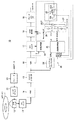
図1は、本発明に係るPLL回路(位相同期回路)を採用した光ディスク装置のRF信号処理系の一実施形態を示すシステム構成図である。 FIG. 1 is a system configuration diagram showing an embodiment of an RF signal processing system of an optical disc apparatus employing a PLL circuit (phase synchronization circuit) according to the present invention.
本光ディスク装置10は、図1に示すように、記録媒体としての光ディスク11、光学ヘッド12、プリアンプ13、AGC(Auto Gain Control)回路14、アナログイコライザ15、アナログデジタルコンバータ(ADC)16、FIRフィルタ17、ビタビ復号器18、デコーダ(ECC、インタフェース(I/F)19、エンコーダ20、レーザドライバ21、位相比較器22、VCO23、ヒステリシスコンパレータ24、周波数比較器25、チャージポンプ回路26、およびループフィルタ27を有している。
As shown in FIG. 1, the
これらの構成要素のうち、位相比較器22、VCO23、ヒステリシスコンパレータ24、周波数比較器25、チャージポンプ回路26、およびループフィルタ27により本発明のPLL回路30が構成されている。そして、チャージポンプ回路26、およびループフィルタ27により本発明の帰還回路が構成される。また、ヒステリシスコンパレータ24および周波数比較器25により周波数比較部が構成される。
以下、このPLL回路の構成要素の具体的な機能を中心に説明する。
Among these components, the
Hereinafter, the specific functions of the components of the PLL circuit will be mainly described.
光ディスク装置10において、光学ヘッド12から出力されプリアンプ13で増幅された再生信号は、AGC回路14で振幅調整され、アナログイコライザ回路15に入力される。
アナログイコライザ15により等化され、高域ノイズを除去された再生信号は、ADC16およびヒステリシスコンパレータ24に入力される。
ADC16の出力は、PLL回路の位相比較器22に入力され、後述するようにPLL回路40においてVCO23をコントロールしてADC15のサンプリング位相を一致させるように制御される。
また、ADC15の出力はFIRフィルタ17に入力され、さらに高精度に等化された後、ビタビ復号器18に入力され、デコード、エラー訂正されたのち、NRZデータとして出力される。
また、NRZデータはエンコーダ20でエンコードされ、この結果に基づいて、レーザドライバ21により光学ヘッド12のレーザが駆動制御される。
In the
The reproduction signal equalized by the
The output of the ADC 16 is input to the
Further, the output of the
The NRZ data is encoded by the
以下、PLL回路について具体的に説明する。 Hereinafter, the PLL circuit will be specifically described.
位相比較器22は、ADC15によるデジタル信号の位相とVCO23の出力クロック(A)の位相を比較し、位相誤差データS22をループフィルタ27に出力する。
The
VCO23は、インバータ231〜233の3段リング構成になっており、ループフィルタ27で位相誤差データS22を積分して得られた制御信号S27により発振周波数が制御される。
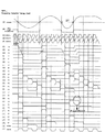
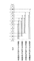
VCO23は、3段リング構成の各段からの出力は、図2(C),(D),(E)に示すようなCLKの一周期を3分割する3相クロックA,B,Cとなっており、これら3相クロックCLKA,CLKB,CLKCは周波数比較器25に供給される。
VCO23の第1相クロック(インバータ233の出力クロック)は、ADC16、FIRフィルタ17、ビタビ復号器18、および位相比較器22に供給される。
The
The
The first phase clock (output clock of the inverter 233) of the
ヒステリシスコンパレータ24は、アナログイコライザ15による、たとえば図2(A)に示すような正弦波状のRF再生信号を受けて、ヒステリシス点に対応してレベルが変化する図2(B)に示すようなヒステリシス信号HYSを周波数比較器25に出力する。
The
PLL回路により、ADC16のサンプリング位相を正しい状態に一致させる必要があるが、入力信号周波数とクロック周波数のずれが大きい場合(3%前後を超える場合)には位相検出器による位相引き込みは困難であるため、まず周波数ループにより周波数ずれを引き込む必要がある。
周波数比較器25は、この周波数ループの初段部に配置されている。
Although it is necessary to match the sampling phase of the ADC 16 to the correct state by the PLL circuit, it is difficult to pull in the phase by the phase detector when the difference between the input signal frequency and the clock frequency is large (over about 3%). Therefore, first, it is necessary to draw a frequency shift by the frequency loop.
The
周波数比較器25は、VCO23による3相クロックCLKA,CLKB,CLKCに同期してヒステリシスコンパレータ24によるヒステリシス信号HYCを取り込み、以降、たとえば第1相クロックAに同期して、入力データ信号のヒステリシスのエッジがどの位相からどの位相に変化したか観察することにより周波数が高いか低いかを周波数誤差として検出して、アップ信号UPまたはダウン信号DOWNをチャージポンプ回路27に出力する。
また、周波数比較器25は、ヒステリシスコンパレータ24の出力パルスHYCを入力して、周波数誤差(UPまたはDOWN)の検出に用いるが、以下に説明するように、ヒステリシスコンパレータ24にて取り除くことができなかった2Tパターンを、VCO23による3相クロックCLKA,CLKB,CLKCに同期してパルスの周期計測を行うことにより除去する。
The
The
このように、周波数比較器25は、入力アナログ信号のエッジ周期をVCOクロックにより計測する。本実施形態では、この入力信号としては、アナログ信号のゼロクロスコンパレータ出力を使用するのではなく、ヒステリシスコンパレータ24の出力パルス(ヒステリシス信号HYS)を使用する。
Thus, the
Blu−rayディスクの場合、ユーザーデータパターンとして2T〜8Tが存在しているが、最短パターンの2Tでは記録再生系の周波数特性により振幅が小さいために、他のパターンに比較して波形間干渉の影響が大きく、その周期が干渉によって変化してしまう。そのため、周波数比較器25に入力する前に、周期の信頼性が低い2Tパターンを振幅の差を利用して取り除く。
Blu−rayディスク等の高密度記録装置においては、劣化した識別S/Nを補うために、記録再生系の周波数特性と近似した特性に等化する、パーシャルレスポンス等化器と最尤復号装置(ビタビ復号器)を組み合わせた、PRML信号処理が採用される。
In the case of a Blu-ray disc, 2T to 8T exist as user data patterns. However, the 2T of the shortest pattern has a smaller amplitude due to the frequency characteristics of the recording / reproducing system. The influence is great, and the period changes due to interference. Therefore, before being input to the
In a high-density recording device such as a Blu-ray disc, a partial response equalizer and a maximum likelihood decoding device (equal to characteristics approximate to the frequency characteristics of the recording / reproducing system) are used to compensate for the deteriorated identification S / N. PRML signal processing combined with a Viterbi decoder) is employed.
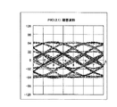
図3は、最短パターンが2Tである1-7PP変調が採用されたBlu−rayディスクにおいて、PR(1,2,1)に等化された再生RF信号の理想アイパターンを示す図である。また、図4は、最短パターンが2Tである1-7PP変調が採用されたBlu−rayディスクにおいて、PR(1,2,1)に等化された再生RF信号の実機アイパターンを示す図である。 FIG. 3 is a diagram showing an ideal eye pattern of a reproduction RF signal equalized to PR (1, 2, 1) in a Blu-ray disc adopting 1-7PP modulation having a shortest pattern of 2T. FIG. 4 is a diagram showing an actual eye pattern of a reproduction RF signal equalized to PR (1, 2, 1) in a Blu-ray disc adopting 1-7PP modulation having a shortest pattern of 2T. is there.
図3に示すように、パーシャルレスポンス等化された再生RF信号は、最短パターンである2RTの振幅が、3T以上のパターンの振幅より、有意差を持って小さいため、コンパレータのヒステリシスレベルを適切な値に設定することにより、取り除くことができる。
ここで、パーシャルレスポンスのクラスはPR(1,2,1)には限定されない。また、最短パターンも2Tには限定されず、DVDのEFMpulsに代表される3T系の変調でもかまわない。
しかし、実機の波形においては、図4のアイパターンが示すように、ノイズや等化誤差による符号間干渉が存在するため、コンパレータのヒステリシスだけでは、2Tを完全に取り除くことはできない。
As shown in FIG. 3, the reproduction response RF signal that has been subjected to partial response equalization has an amplitude of 2RT, which is the shortest pattern, which is significantly smaller than the amplitude of a pattern of 3T or more, so that the hysteresis level of the comparator is set appropriately. It can be removed by setting the value.
Here, the partial response class is not limited to PR (1,2,1). The shortest pattern is not limited to 2T, and 3T modulation represented by DVD EFMpuls may be used.
However, as shown by the eye pattern in FIG. 4, in the actual machine waveform, there is intersymbol interference due to noise and equalization error. Therefore, 2T cannot be completely removed only by the hysteresis of the comparator.
ヒステリシスコンパレータ24の出力パルスHYSは、PLL30の周波数比較器25に入力され、周波数誤差の方向(UPまたはDOWN)の検出に用いられる。
このとき、ヒステリシスコンパレータ24にて取り除くことができなかった2Tパターンを、VCOクロックによってパルスの周期計測を行うことにより除去する。
The output pulse HYS of the
At this time, the 2T pattern that could not be removed by the
周期計測で2Tパターンを取り除く場合には、3Tパターンの分布と2Tパターンの分布が重なっているため、2Tだけを取り除くことが難しい。
このため、周期計測単独で2Tを取り除こうとした場合には、特に2T周期の変化により2Tの分布が3T側に移動している場合には、2Tの取れ残り成分により3Tパターンの分布が非対称になり、周波数比較の対称性が劣化してしまうおそれがある。
これに対してヒステリシスコンパレータ24による2T除去においては、2T、3Tの分布対称性を確保することができ、2Tの分布をある程度取り除くことができる。
したがって、これら二つの方法を併用することにより、精度良く2Tを取り除くことができる。
When removing a 2T pattern by period measurement, it is difficult to remove only 2T because the distribution of the 3T pattern and the distribution of the 2T pattern overlap.
For this reason, when trying to remove 2T by periodic measurement alone, especially when the 2T distribution is moved to the 3T side due to a change in the 2T period, the distribution of the 3T pattern becomes asymmetric due to the remaining 2T component. Therefore, the symmetry of frequency comparison may be deteriorated.
On the other hand, in 2T removal by the
Therefore, 2T can be accurately removed by using these two methods together.
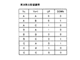
図5は、本実施形態に係る周波数比較器の基本的な動作イメージを示す図である。また、図6は、本実施形態に係る周波数比較器の比較論理を示す図である。 FIG. 5 is a diagram illustrating a basic operation image of the frequency comparator according to the present embodiment. FIG. 6 is a diagram showing the comparison logic of the frequency comparator according to the present embodiment.
図5に示すように、3相クロックである第1相クロックCLKA、第2相クロックCLKB、第3相クロックCLKCにより、1クロックCLK区間を3分割し、各位相区間をA、B、Cとする。
このとき、入力データ信号のヒステリシスの現在のエッジYnと次のエッジYn+1 の位相の遷移から周波数誤差(の方向)を次のようにして検出する。
As shown in FIG. 5, one clock CLK section is divided into three by the first phase clock CLKA, the second phase clock CLKB, and the third phase clock CLKC, which are three phase clocks, and each phase section is divided into A, B, and C. To do.
At this time, the frequency error (direction) is detected from the phase transition of the current edge Yn and the next edge Yn + 1 of the hysteresis of the input data signal as follows.
クロックCLK1周期内の各位相A、B、Cに対して、エッジの遷移が順方向(A→B→C)であれば、入力信号周波数はVCO周波数よりも低いと考えられるため、ダウン信号DOWNを出力する。
エッジの遷移が逆方向(C→B→A)であれば、入力データ信号の周波数はVCO周波数よりも高いと考えられるため、アップ信号UPを出力する。
エッジの位相遷移がない場合には、誤差検出はできないため、何も出力されない。
If the transition of the edge is forward (A → B → C) for each phase A, B, C in the clock CLK1 period, the input signal frequency is considered to be lower than the VCO frequency, so the down signal DOWN Is output.
If the edge transition is in the reverse direction (C → B → A), the frequency of the input data signal is considered to be higher than the VCO frequency, and therefore the up signal UP is output.
If there is no edge phase transition, no error is detected, so nothing is output.
具体的には、図6に示すように、周波数比較器25は、エッジYnが位相Aで次のエッジYn+1 が位相Aの場合には、エッジの位相遷移がなく誤差検出はできないため、アップ信号UPもダウン信号DOWNも出力しない。
エッジYnが位相Aで次のエッジYn+1 が位相Bの場合には、入力データ信号の周波数はVCO周波数よりも低いと考えられるため、ダウン信号DOWNを出力する。
エッジYnが位相Aで次のエッジYn+1 が位相Cの場合には、入力データ信号の周波数はVCO周波数よりも高いと考えられるため、アップ信号UPを出力する。
エッジYnが位相Bで次のエッジYn+1 が位相Aの場合には、入力データ信号の周波数はVCO周波数よりも高いと考えられるため、アップ信号UPを出力する。
エッジYnが位相Bで次のエッジYn+1 が位相Bの場合には、エッジの位相遷移がなく誤差検出はできないため、アップ信号UPもダウン信号DOWNも出力しない。
エッジYnが位相Bで次のエッジYn+1 が位相Cの場合には、入力データ信号の周波数はVCO周波数よりも低いと考えられるため、ダウン信号DOWNを出力する。
エッジYnが位相Cで次のエッジYn+1 が位相Aの場合には、入力データ信号の周波数はVCO周波数よりも低いと考えられるため、ダウン信号DOWNを出力する。
エッジYnが位相Cで次のエッジYn+1 が位相Bの場合には、入力データ信号の周波数はVCO周波数よりも高いと考えられるため、アップ信号UPを出力する。
エッジYnが位相Cで次のエッジYn+1 が位相Cの場合には、エッジの位相遷移がなく誤差検出はできないため、アップ信号UPもダウン信号DOWNも出力しない。
Specifically, as shown in FIG. 6, when the edge Yn is the phase A and the next edge Yn + 1 is the phase A, the
When the edge Yn is the phase A and the next edge Yn + 1 is the phase B, the frequency of the input data signal is considered to be lower than the VCO frequency, so the down signal DOWN is output.
When the edge Yn is the phase A and the next edge Yn + 1 is the phase C, the up signal UP is output because the frequency of the input data signal is considered to be higher than the VCO frequency.
When the edge Yn is the phase B and the next edge Yn + 1 is the phase A, the frequency of the input data signal is considered to be higher than the VCO frequency, so the up signal UP is output.
When the edge Yn is the phase B and the next edge Yn + 1 is the phase B, there is no phase transition of the edge and the error cannot be detected, so neither the up signal UP nor the down signal DOWN is output.
When the edge Yn is the phase B and the next edge Yn + 1 is the phase C, the frequency of the input data signal is considered to be lower than the VCO frequency, so the down signal DOWN is output.
When the edge Yn is the phase C and the next edge Yn + 1 is the phase A, the frequency of the input data signal is considered to be lower than the VCO frequency, so the down signal DOWN is output.
When the edge Yn is the phase C and the next edge Yn + 1 is the phase B, the up signal UP is output because the frequency of the input data signal is considered to be higher than the VCO frequency.
When the edge Yn is the phase C and the next edge Yn + 1 is the phase C, there is no phase transition of the edge and the error cannot be detected, so neither the up signal UP nor the down signal DOWN is output.
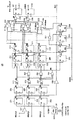
図7は、図5の検出動作を可能にする周波数比較器のロジック回路の一例を示す回路図である。 FIG. 7 is a circuit diagram showing an example of a logic circuit of a frequency comparator that enables the detection operation of FIG.
図7の周波数比較器25は、D型フリップフロップ201〜218、排他的論理和(EXOR)ゲート219〜221、負入力を含む2入力ANDゲート222、負入力を含む3入力ANDゲート223、3入力ORゲート224〜226、2入力NORゲート227、スイッチ回路228〜230、負入力を含む3入力ANDゲート231、3入力ANDゲート232〜235、負入力を含む4入力ANDゲート236、および第1相クロックCLKAを遅延等させるためのバッファ237,238を有している。
7 includes D-type flip-
フリップフロップ201〜203はヒステリシス信号HYCの入力HYCINに対して並列に配置されている。フリップフロップ201は第1相クロックCLKAに同期してヒステリシス信号HYCをラッチし、フリップフロップ202は第2相クロックCLKBに同期してヒステリシス信号HYCをラッチし、フリップフロップ203は第3相クロックCLKCに同期してヒステリシス信号HYCをラッチする。
すなわち、フリップフロップ201〜203は周波数比較器25の入力段に配置されて、VCO23の3相クロックCLKA,CLKB,CLKCに同期して、ヒステリシスコンパレータ24によるヒステリシス信号HYCをラッチする。
図2(F)〜(H)にフリップフロップ201〜203のQ出力をそれそれA0,B0,C0として示している。
なお、初段以降の各フリップフロップ204〜218は、第1相クロックCLKAに同期してデータの入出力を行う。
The flip-
That is, the flip-
2F to 2H show the Q outputs of the flip-
Note that the flip-
フリップフロップ204のD入力は初段のフリップフロップ201のQ出力に接続され、フリップフロップ205のD入力は初段のフリップフロップ202のQ出力に接続され、フリップフロップ206のD入力は初段のフリップフロップ203のQ出力に接続されている。
フリップフロップ204〜206は、バッファ237を介した第1相クロックCLKAに同期してそれぞれフリップフロップ201〜203の出力をラッチする。
図2(I)〜(K)にフリップフロップ204〜206のQ出力をそれそれA1,B1,C1として示している。
The D input of the flip-
The flip-
2 (I) to (K) show the Q outputs of the flip-
EXOR219は、フリップフロップ204の出力A1とフリップフロップ205の出力B1との排他的論理和をとり、その結果をスイッチ228のH入力、ANDゲート222の負入力、ANDゲート223の第1負入力、およびORゲート224の第1入力に供給する。
EXOR220は、フリップフロップ205の出力B1とフリップフロップ206の出力C1との排他的論理和をとり、その結果をアンドゲート222の正入力、アンドゲート223の第2負入力、およびORゲート224の第2入力に供給する。
EXOR221は、フリップフロップ206の出力B1と初段のフリップフロップ201の出力A0との排他的論理和をとり、その結果をアンドゲート223の正入力、およびORゲート224の第3入力に供給する。
これら3つのEXOR219〜221は今のクロックを得るために設けられており、クロックCLKA,CLKB,CLKCのいずれか一つを取り出す。
図2(L)〜(N)にEXOR218〜220の出力をそれそれA2,B2,C2として示している。
EXOR219〜222の出力A2,B2,C2はヒステリシスがあるときにいずれかがハイレベルとなる。この例では、EXOR221の出力C2がハイレベルとなっている。
The
The
The
These three
2 (L) to (N) show the outputs of
One of the outputs A2, B2, and C2 of the
ANDゲート222の出力はスイッチ回路229のH入力に供給され、ANDゲート23の出力はスイッチ回路230のH入力に供給される。
ORゲート224は、EXOR219〜221の出力A2,B2,C2の論理和をとり、スイッチ信号SWとしてスイッチ回路228〜230、およびフリップフロップ213のD入力に出力する。
The output of the AND
The OR
スイッチ回路228〜230は、スイッチ信号SWがハイレベルの場合にはヒステリシス点が検出されたものとしてH入力を選択して次段の対応するフリップフロップ207〜209のD入力に出力する。
スイッチ回路228〜230は、スイッチ信号SWがローレベルの場合にはヒステリシス点が検出されていないものとしてL入力を選択して次段の対応するフリップフロップ207〜209のQ出力をD入力に入力させるループを形成する。
図2(O)にORゲート224の出力であるスイッチ信号SWを示している。
When the switch signal SW is at a high level, the switch circuits 228 to 230 select the H input on the assumption that a hysteresis point has been detected, and output it to the D inputs of the corresponding flip-
When the switch signal SW is at a low level, the switch circuits 228 to 230 select the L input on the assumption that the hysteresis point is not detected, and input the Q outputs of the corresponding flip-
FIG. 2O shows the switch signal SW that is the output of the
フリップフロップ207〜209は、上述したように対応するスイッチ回路228〜230の出力を、バッファ237,238を介した第1相クロックCLKAに同期して取り込む。
フリップフロップ207〜209は、ヒステリシスが検出されていない間は、スイッチ回路228〜230で形成されるループによる前回ラッチしたデータを、第1相クロックCLKAに同期してラッチし続け、ヒステリシスが検出された場合に、スイッチ回路229〜230を通して検出時点のデータを第1相クロックCLKAに同期してラッチする。
フリップフロップ207のQ出力は、スイッチ回路228のL入力、次段のフリップフロップ210のD入力、ANDゲート233の第1入力に、およびANDゲート236の第3入力に供給される。
フリップフロップ208のQ出力は、スイッチ回路229のL入力、次段のフリップフロップ211のD入力、ANDゲート232の第3入力、およびANDゲート235の第2入力に供給される。
フリップフロップ209のQ出力は、スイッチ回路230のL入力、次段のフリップフロップ212のD入力、ANDゲート231の第3入力、およびANDゲート234の第3入力に供給される。
図2(U)〜(W)にフリップフロップ207〜209のQ出力をそれそれA3,B3,C3として示している。
As described above, the flip-
While the hysteresis is not detected, the flip-
The Q output of the flip-
The Q output of the flip-
The Q output of the flip-
2 (U) to (W) show the Q outputs of the flip-
フリップフロップ210〜212は、バッファ237,238を介した第1相クロックCLKAに同期してそれぞれフリップフロップ207〜209の出力をラッチする。
フリップフロップ210の出力は、ANDゲート231の第1入力、およびANDゲート232の第1入力に供給される。
フリップフロップ211の出力は、ANDゲート233の第2入力、およびANDゲート234の第1入力に供給される。
フリップフロップ212の出力は、ANDゲート235の第1入力、およびANDゲート236の第2入力に供給される。
図2(X)〜(Z)にフリップフロップ210〜212のQ出力をそれそれA4,B4,C4として示している。
The flip-
The output of the flip-
The output of the flip-
The output of flip-
2 (X) to (Z) show the Q outputs of the flip-
フリップフロップ213は、バッファ237,238を介した第1相クロックCLKAに同期してORゲート224の出力信号SWをラッチする。
フリップフロップ213のQ出力は、次段のフリップフロップ214のD入力に供給される。
フリップフロップ214は、バッファ237,238を介した第1相クロックCLKAに同期してフリップフロップ213の出力をラッチする。
フリップフロップ214のQ出力は、次段のフリップフロップ215のD入力、NORゲート227の第1入力、およびANDゲートの第2入力(負入力)に供給される。
フリップフロップ215は、バッファ237,238を介した第1相クロックCLKAに同期してフリップフロップ214の出力をラッチする。
フリップフロップ215のQ出力は、次段のフリップフロップ216のD入力、およびNORゲート227の第2入力に供給される。
フリップフロップ216は、バッファ237,238を介した第1相クロックCLKAに同期してフリップフロップ215の出力をラッチする。
フリップフロップ216のQ出力は、ANDゲート236の第4入力(負入力)に供給される。
フリップフロップ214〜216は、イネーブル信号ENBによりイネーブルとなる。 図2(Q)〜(S)にフリップフロップ213〜216のQ出力をそれそれP0,P1,P2,P3として示している。
The flip-
The Q output of the flip-
The flip-
The Q output of the flip-
The flip-
The Q output of the flip-
The flip-
The Q output of the flip-
The flip-
NORゲート227の出力は、ANDゲート232の第3入力、ANDゲート233の第3入力、ANDゲート234の第2入力、ANDゲート235の第3入力、およびANDゲート236の第1入力に供給される。
図2(T)にNORゲート227の出力をP4として示している。
The output of the NOR
FIG. 2 (T) shows the output of the NOR
フリップフロップ213〜216、およびNORゲート227は、ロジック動作としては、基本的には2Tパターン(およびノイズその他の要因により発生した1T)による周波数比較結果をマスクするため、現在のデータエッジの1クロックまたは2クロック前にデータエッジが存在した場合には、2T以下と判断して出力をマスクする。
Since the flip-
ANDゲート231は、図6の論理に基づいて、エッジYnが位相Aで次のエッジYn+1 が位相Cの場合には、入力データ信号の周波数はVCO周波数よりも高いものとして、アップ信号UPを出力させるためにハイレベルの信号をORゲート225の第1入力に供給する。
ANDゲート232は、図6の論理に基づいて、前回のエッジYnが位相Aで次のエッジYn+1 が位相Bの場合には、入力データ信号の周波数はVCO周波数よりも低いものとして、ダウン信号DOWNを出力させるためにハイレベルの信号をORゲート226の第1入力に供給する。
ANDゲート231および232は、エッジYnが位相Aで次のエッジYn+1 が位相Aの場合には、エッジの位相遷移がなく誤差検出はできないため、アップ信号UPもダウン信号DOWNも出力しないようにローレベルの信号をそれぞれゲート225,226に出力する。
Based on the logic of FIG. 6, the AND
Based on the logic of FIG. 6, the AND
When the edge Yn is phase A and the next edge Yn + 1 is phase A, the AND
ANDゲート233は、図6の論理に基づいて、前回のエッジYnが位相Bで次のエッジYn+1 が位相Aの場合には、入力データ信号の周波数はVCO周波数よりも高いものとして、アップ信号UPを出力させるためにハイレベルの信号をORゲート225の第2入力に供給する。
ANDゲート234は、図6の論理に基づいて、前回のエッジYnが位相Bで次のエッジYn+1 が位相Cの場合には、入力データ信号の周波数はVCO周波数よりも低いものとして、ダウン信号DOWNを出力させるために、ハイレベルの信号をORゲート226の第2入力に供給する。
ANDゲート233および234は、エッジYnが位相Bで次のエッジYn+1 が位相Bの場合には、エッジの位相遷移がなく誤差検出はできないため、アップ信号UPもダウン信号DOWNも出力しないようにローレベルの信号をそれぞれゲート225,226に出力する。
Based on the logic of FIG. 6, the AND
Based on the logic of FIG. 6, the AND
When the edge Yn is phase B and the next edge Yn + 1 is phase B, the AND
ANDゲート235は、図6の論理に基づいて、前回のエッジYnが位相Cで次のエッジYn+1 が位相Bの場合には、入力データ信号の周波数はVCO周波数よりも高いものとして、アップ信号UPを出力させるためにハイレベルの信号をORゲート225の第3入力に供給する。
ANDゲート236は、図6の論理に基づいて、前回のエッジYnが位相Cで次のエッジYn+1 が位相Aの場合には、入力データ信号の周波数はVCO周波数よりも低いものとして、ダウン信号DOWNを出力させるために、ハイレベルの信号をORゲート226の第3入力に供給する。
ANDゲート235および236は、エッジYnが位相Cで次のエッジYn+1 が位相Cの場合には、エッジの位相遷移がなく誤差検出はできないため、アップ信号UPもダウン信号DOWNも出力しないようにローレベルの信号をそれぞれゲート225,226に出力する。
Based on the logic of FIG. 6, the AND
Based on the logic of FIG. 6, the AND
When the edge Yn is phase C and the next edge Yn + 1 is phase C, the AND
ORゲート225は、ANDゲート231、233、235の出力信号の論理和をとり、アップ信号UPの出力段のフリップフロップ217のD入力に供給する。
ORゲート226は、ANDゲート232、234、236の出力信号の論理和をとり、ダウン信号DWMの出力段のフリップフロップ218のD入力に供給する。
図2(Γ),(Δ)にORゲート225,226の出力をそれそれU0,D0として示している。
The OR
The OR
2 (Γ) and (Δ) show the outputs of the
フリップフロップ217は、バッファ237,238を介した第1相クロックCLKAに同期してORゲート225のハイレベルまたはローレベルをとる出力U0をラッチして、Q出力からアップ信号UPをチャージポンプ回路26に出力する。
フリップフロップ218は、バッファ237,238を介した第1相クロックCLKAに同期してORゲート226のハイレベルまたはローレベルをとる出力D0をラッチして、Q出力からダウン信号DOWNをチャージポンプ回路26に出力する。
図2(Π),(Σ)にフリップフロップ217,218の出力であるアップ信号UPおよびダウン信号DOWNをそれそれ示している。
The flip-flop 217 latches the output U0 that takes the high level or low level of the
The flip-
2 (Π) and (Σ) show the up signal UP and the down signal DOWN which are the outputs of the flip-
なお、フリップフロップ217,218に供給される第1相クロックCLKAは、たとえば図示しない分周器(たとえば2分周)により分周した後の第1相クロックCLK2として、アップ信号UPおよびダウン信号DOWNをラッチし、出力するように構成することも可能である。
図2(Υ)にこのクロックCLK2を示している。
The first phase clock CLKA supplied to the flip-
FIG. 2 (Υ) shows this clock CLK2.
なお、図7の周波数比較器25では、フリップフロップ210〜212には前回のヒステリシスがいずれの相で検出されたかを示すデータがセットされ、フリップフロップ207〜209には今回(次の)のヒステリシスがいずれの相で検出されたかを示すデータがセットされることから、前回のエッジYnの検出位相の情報と次のエッジYn+1 の検出位相の情報が得られている。
In the
そして、本実施形態において設けられたフリップフロップ213〜216は、周波数比較器25における2T除去ロジック系として機能する。
The flip-
図8は、3相クロックを使用したパルスエッジ周期計測による2T判定方法を説明するための図である。 FIG. 8 is a diagram for explaining a 2T determination method based on pulse edge period measurement using a three-phase clock.
3相クロックであるCLKA、CLKB、CLKC、により、1CLK区間を3分割し、各位相区間をA、B、Cとする。
このとき入力データパルスの現在のエッジと次のエッジが各位相のどこにあるか、および2つのエッジ間にVCOクロックが何発存在したかによって、VCO23のクロックの3倍の精度で周期計測を行う。
なお、計測用のクロックは3相である必要性はなく、より分解能を高くするために、4相以上に多相化してもよい。
また、ヒステリシスコンパレータ24のヒステリシスレベルは調整可能であり、最適な値に設定できる。
A CLK section is divided into three by CLKA, CLKB, and CLKC, which are three-phase clocks, and A, B, and C are defined as each phase section.
At this time, period measurement is performed with an accuracy three times that of the clock of the
Note that the measurement clock does not have to be three-phase, and may be multi-phased to four or more phases in order to increase the resolution.
Further, the hysteresis level of the
ロジック動作としては、基本的には2Tパターン(およびノイズその他の要因により発生した1T)による周波数比較結果をマスクするため、現在のデータエッジの1クロックまたは2クロック前にデータエッジが存在した場合には、2T以下と判断して出力をマスクする構成となっているが、このとき、例外として以下のパターンが存在する。
(1)Aを起点として2クロック後のCを終点とする3Tパターン、
(2)Cを起点として、3クロック後のAを終点とする2Tパターン、である。
The logic operation basically masks the frequency comparison result based on the 2T pattern (and 1T generated by noise and other factors), so that the data edge exists one or two clocks before the current data edge. Is configured to mask the output by judging that it is 2T or less. However, the following pattern exists as an exception.
(1) 3T pattern starting from A and ending C after 2 clocks,
(2) A 2T pattern starting from C and ending at A after 3 clocks.
(1)については、このままでは3Tパターンも除去してしまうため、A→Cの遷移に対しては、1クロック前にデータエッジが存在した時のみマスクする。
(2)については、2Tパターンの取り残りが発生するため、C→Aの遷移については、3クロック前までのデータエッジの存在によりマスクする。
As for (1), since the 3T pattern is also removed as it is, the transition from A to C is masked only when a data edge exists one clock before.
As for (2), since a 2T pattern is left behind, the transition from C to A is masked by the presence of data edges up to three clocks before.
以上のように、ヒステリシスコンパレータ24とパターン周期計測を併用することにより、2Tパターンを精度良く取り除くことができ、この結果として周波数比較器25の誤動作を防止することができる。
As described above, by using the
本実施形態における周波数比較器25は、第1相クロックCLKAの1周期以内にヒステリシスが2度検出されることは、データの特性上ありえないことから、もし、1T内に検出位相に変化があると、ノイズ等に基づくデータを取り込んだものとして、アップ信号UPおよびダウン信号DOWNを出力させず、無視させる。
In the
たとえば、正常動作の場合には、前回のエッジYnが位相Aで次のエッジYn+1 が位相Bの場合には、フリップフロップ210の出力A4、フリップフロップ208の出力B3がハイレベルで、かつ、NORゲート227の出力もハイレベルであるはずであることから、ANDゲート232においては、入力データ信号の周波数はVCO周波数よりも低いものとして、ダウン信号DOWNを出力させるためにハイレベルの信号をORゲート226に供給する。
しかし、ノイズ等のために、NORゲート227の出力がローレベルである場合には、ANDゲート232の出力はマスクされてローレベルに保持され、ダウン信号DOWNの出力が抑止される。
For example, in the normal operation, when the previous edge Yn is phase A and the next edge Yn + 1 is phase B, the output A4 of the flip-
However, when the output of the NOR
同様に、正常動作の場合には、前回のエッジYnが位相Bで次のエッジYn+1 が位相Aの場合には、フリップフロップ207の出力A3、フリップフロップ211の出力B4がハイレベルで、かつ、NORゲート227の出力もハイレベルであるはずであることから、ANDゲート233においては、入力データ信号の周波数はVCO周波数よりも高いものとして、アップ信号UPを出力させるためにハイレベルの信号をORゲート225の供給する。
しかし、ノイズ等のために、NORゲート227の出力がローレベルである場合には、ANDゲート233の出力はマスクされてローレベルに保持され、アップ信号UPの出力が抑止される。
Similarly, in the normal operation, when the previous edge Yn is phase B and the next edge Yn + 1 is phase A, the output A3 of the flip-
However, when the output of the NOR
同様に、正常動作の場合には、前回のエッジYnが位相Bで次のエッジYn+1 が位相Cの場合には、フリップフロップ209の出力C3、フリップフロップ211の出力B4がハイレベルで、かつ、NORゲート227の出力もハイレベルであるはずであることから、ANDゲート234においては、入力データ信号の周波数はVCO周波数よりも低いものとして、ダウン信号DOWNを出力させるためにハイレベルの信号をORゲート226に供給する。
しかし、ノイズ等のために、NORゲート227の出力がローレベルである場合には、ANDゲート234の出力はマスクされてローレベルに保持され、ダウン信号DOWNの出力が抑止される。
Similarly, in the normal operation, when the previous edge Yn is phase B and the next edge Yn + 1 is phase C, the output C3 of the flip-
However, when the output of the NOR
同様に、正常動作の場合には、前回のエッジYnが位相Cで次のエッジYn+1 が位相Bの場合には、フリップフロップ208の出力B3、フリップフロップ212の出力C4がハイレベルで、かつ、1のゲート227の出力もハイレベルであるはずであることから、ANDゲート235においては、入力データ信号の周波数はVCO周波数よりも高いものとして、アップ信号UPを出力させるためにハイレベルの信号をORゲート225に供給する。
しかし、ノイズ等のために、NORゲート227の出力がローレベルである場合には、ANDゲート235の出力はマスクされてローレベルに保持され、アップ信号UPの出力が抑止される。
Similarly, in the normal operation, when the previous edge Yn is the phase C and the next edge Yn + 1 is the phase B, the output B3 of the flip-
However, when the output of the NOR
同様に、正常動作の場合には、前回のエッジYnが位相Cで次のエッジYn+1 が位相Aの場合には、フリップフロップ207の出力A3、フリップフロップ212の出力C4がハイレベルで、かつ、NORゲート227の出力もハイレベルであるはずであることから、ANDゲート236においては、入力データ信号の周波数はVCO周波数よりも低いものとして、ダウン信号DOWNを出力させるためにハイレベルの信号をORゲート226に供給する。
しかし、ノイズ等のために、NORゲート227の出力がローレベルである場合には、ANDゲート236の出力はマスクされてローレベルに保持され、ダウン信号DOWNの出力が抑止される。
Similarly, in the normal operation, when the previous edge Yn is the phase C and the next edge Yn + 1 is the phase A, the output A3 of the flip-
However, when the output of the NOR
次に、図1の回路の動作を説明する。 Next, the operation of the circuit of FIG. 1 will be described.
光学ヘッド12から出力されプリアンプ13で増幅された再生信号は、AGC回路14で振幅調整され、アナログイコライザ回路15に入力される。
アナログイコライザ15により等化され、高域ノイズを除去された再生信号は、ADC16およびヒステリシスコンパレータ24に入力される。
The reproduction signal output from the
The reproduction signal equalized by the
このとき、PLL回路30によりADC16のサンプリング位相を正しい状態に一致させる必要があるが、入力信号周波数とクロック周波数のずれが大きい場合(3%前後を超える場合)には位相検出器による位相引き込みは困難であるため、まず周波数ループにより周波数ずれを引き込む。
At this time, it is necessary to match the sampling phase of the ADC 16 to the correct state by the
ヒステリシスコンパレータ24の出力は、PLL回路30の周波数比較器25に入力され、周波数誤差の方向(UPまたはDOWN)の検出に用いられる。
The output of the
周波数比較器25においてはは、VCO23による3相クロックCLKA,CLKB,CLKCに同期してヒステリシスコンパレータ24によるヒステリシス信号HYCを取り込み、以降、たとえば第1相クロックAに同期して、入力データ信号のヒステリシスのエッジがどの位相からどの位相に変化したか観察することにより周波数が高いか低いかを周波数誤差として検出され、アップ信号UPまたはダウン信号DOWNがチャージポンプ回路27に出力される。
このとき、周波数比較器25においては、ヒステリシスコンパレータ24の出力パルスHYCを入力して、周波数誤差(UPまたはDOWN)の検出に用いるが、ヒステリシスコンパレータ24にて取り除くことができなかった2Tパターンを、VCO23による3相クロックCLKA,CLKB,CLKCに同期してパルスの周期計測を行うことにより除去される。
In the
At this time, in the
周波数比較器25から出力されたアップ信号UPまたはダウン信号DOWNは周波数ループ用のチャージポンプ回路26にて電流に変換され、ループフィルタ27に積分される。
ループフィルタ27の出力制御信号S27によりVCO23の発振周波数がコントロールされ、入力データ信号の周波数に一致させるように動作する。
VCO23は、3段リング構成になっており、各段からの出力はCLKの一周期を3分割する3相クロックCLKA,CLKB,CLKCとなっている。この3相クロックCLKA,CLKB,CLKCが周波数比較器25に入力され、ヒステリシスコンパレータ24から出力されたヒステリシス信号HYCと比較することにより周波数検出が行われる。
The up signal UP or the down signal DOWN output from the
The oscillation frequency of the
The
以上が周波数モードの動作であり、周波数ループの動作により入力データ信号とVCO23の発振周波数がほぼ一致すると、PLL回路30は、位相ロックモードに切り替わる。
The above is the operation in the frequency mode, and when the input data signal and the oscillation frequency of the
ADC16の出力は、PLL回路30の位相比較回路22に入力され、その位相誤差データS22はループフィルタ27で積分され、VCO23をコントロールしてADC16のサンプリング位相を一致させる。
また、ADC16の出力はFIRフィルタ17に入力され、さらに高精度に等化された後、ビタビ復号器18に入力され、デコード、エラー訂正されたのち、NRZデータとして出力される。
The output of the ADC 16 is input to the
The output of the ADC 16 is input to the
以上説明したように、本実施形態によれば、VCO23による3相クロックCLKA,CLKB,CLKCに同期してヒステリシスコンパレータ24によるヒステリシス信号HYCを取り込み、以降、たとえば第1相クロックCLKAに同期して、入力データ信号のヒステリシスのエッジがどの位相からどの位相に変化したか観察することにより周波数が高いか低いかを周波数誤差として検出する際に、ヒステリシスコンパレータ24にて取り除くことができなかった2Tパターンを、VCO23による3相クロックCLKA,CLKB,CLKCに同期してパルスの周期計測を行うことにより除去し、これにより検出結果に基づいたアップ信号UPまたはダウン信号DOWNをチャージポンプ回路26に出力する周波数比較器25を有することから、以下の効果を得ることができる。
As described above, according to the present embodiment, the hysteresis signal HYC is acquired by the
すなわち、本発明によれば、ノイズや符号間干渉による劣化の大きい最短パターンを除去して周波数比較することにより、イコライザの等化誤差や記録パターン、光ピックアップの収差、あるいはディスクのスキューや記録密度によらず、正確な周波数比較が可能となる。
その結果、PLL回路の周波数引き込み動作は安定し、所望のキャプチャレンジを確保することができる。
結果として、高密度光ディスク装置のプレイアビリティを向上させることができる。
That is, according to the present invention, the equalization error of the equalizer, the recording pattern, the aberration of the optical pickup, the disc skew or the recording density is obtained by removing the shortest pattern that is greatly deteriorated due to noise or intersymbol interference and comparing the frequencies. Regardless of this, accurate frequency comparison is possible.
As a result, the frequency pull-in operation of the PLL circuit is stable, and a desired capture range can be ensured.
As a result, the playability of the high density optical disk device can be improved.
10…光ディスク、11…光ディスク、12…光学ヘッド、13…プリアンプ、14…AGC回路、15…アナログイコライザ、16、アナログデジタルコンバータ(ADC)、17…FIRフィルタ、18…ビタビ復号器、19…デコーダ(ECC、インタフェース(I/F)、20…エンコーダ、21…レーザドライバ、22…位相比較器、23…VCO、24…ヒステリシスコンパレータ、25…周波数比較器、26…チャージポンプ回路、27…ループフィルタ、30…PLL回路。
DESCRIPTION OF
Claims (18)
上記発振回路によるクロックと入力信号の位相差を検出し、位相差データを出力する位相比較回路と、
上記位相比較回路の位相差データおよび帰還信号に基づいて上記制御信号を生成し、上記発振回路に供給する帰還回路と、
複数のパターンを含む入力信号から最短パターンのみを除去した信号と上記発振回路のクロックの周波数を比較し、周波数誤差に応じた信号を上記帰還回路に出力する周波数比較部と
を有する位相同期回路。 An oscillation circuit that oscillates at a frequency according to a control signal and outputs a clock of a predetermined frequency;
A phase comparison circuit that detects a phase difference between the clock and the input signal by the oscillation circuit and outputs phase difference data;
A feedback circuit that generates the control signal based on phase difference data and a feedback signal of the phase comparison circuit and supplies the control signal to the oscillation circuit;
A phase synchronization circuit comprising: a frequency comparison unit that compares a signal obtained by removing only the shortest pattern from an input signal including a plurality of patterns with a frequency of a clock of the oscillation circuit and outputs a signal corresponding to a frequency error to the feedback circuit.
請求項1記載の位相同期回路。 2. The phase according to claim 1, wherein the frequency comparison unit includes a hysteresis comparator, removes the shortest pattern having a small amplitude from the input signal through the hysteresis comparator, and compares the output pulse after the removal with the frequency of the clock of the oscillation circuit. Synchronous circuit.
請求項1記載の位相同期回路。 The frequency comparison unit includes a comparator, measures an edge period of an output pulse obtained from the input signal through the comparator, and stops output of a frequency comparison or comparison result in the case of the shortest pattern. Phase synchronization circuit.
請求項3記載の位相同期回路。 The phase synchronization circuit according to claim 3, wherein the comparator is a hysteresis comparator that removes a shortest pattern having a small amplitude of the input signal.
上記周波数比較部は、上記2T〜8Tのデータパターンのうち最短パターンである2Tパターンのみを除去する
請求項1記載の位相同期回路。 The plurality of patterns include 2T to 8T data patterns,
The phase synchronization circuit according to claim 1, wherein the frequency comparison unit removes only the 2T pattern which is the shortest pattern among the 2T to 8T data patterns.
上記周波数比較部は、上記2T〜8Tのデータパターンのうち最短パターンである2Tパターンのみを除去する
請求項2記載の位相同期回路。 The plurality of patterns include 2T to 8T data patterns,
The phase synchronization circuit according to claim 2, wherein the frequency comparison unit removes only the 2T pattern which is the shortest pattern from the 2T to 8T data patterns.
上記発振回路による多相クロックのうちの一のクロックと入力信号の位相差を検出し、位相差データを出力する位相比較回路と、
上記位相比較回路の位相差データおよび帰還信号に基づいて上記制御信号を生成し、上記発振回路に供給する帰還回路と、
複数のパターンを含む入力信号から入力信号の振幅の小さい最短パターンを除去するヒステリシスコンパレータと、
上記ヒステリシスコンパレータの出力パルスおよび上記発振回路の多相クロックに基づいて、当該出力パルスとクロックとの周波数誤差を検出し、周波数誤差に応じた信号を出力し、出力パルスのエッジ周期を計測し、最短パターンの場合には、周波数比較または比較結果の出力を停止する周波数比較器と
を有する位相同期回路。 An oscillation circuit that oscillates at a frequency according to the control signal and outputs a multiphase clock having different phases;
A phase comparison circuit that detects a phase difference between one of the multiphase clocks by the oscillation circuit and an input signal, and outputs phase difference data;
A feedback circuit that generates the control signal based on phase difference data and a feedback signal of the phase comparison circuit and supplies the control signal to the oscillation circuit;
A hysteresis comparator that removes the shortest pattern with a small amplitude of the input signal from an input signal including a plurality of patterns;
Based on the output pulse of the hysteresis comparator and the multi-phase clock of the oscillation circuit, the frequency error between the output pulse and the clock is detected, a signal corresponding to the frequency error is output, the edge period of the output pulse is measured, In the case of the shortest pattern, a phase synchronization circuit having a frequency comparator that stops frequency comparison or comparison result output.
上記周波数比較部は、上記2T〜8Tのデータパターンのうち最短パターンである2Tパターンのみを除去する
請求項7記載の位相同期回路。 The plurality of patterns include 2T to 8T data patterns,
The phase synchronization circuit according to claim 7, wherein the frequency comparison unit removes only the 2T pattern which is the shortest pattern from the 2T to 8T data patterns.
上記クロックによるサンプリング位相を正しい状態に一致させるための位相同期回路を有し、
上記位相同期回路は、
制御信号に応じた周波数をもって発振して所定周波数のクロックを出力する発振回路と、
上記発振回路によるクロックと入力信号の位相差を検出し、位相差データを出力する位相比較回路と、
上記位相比較回路の位相差データおよび帰還信号に基づいて上記制御信号を生成し、上記発振回路に供給する帰還回路と、
複数のパターンを含む入力信号から最短パターンのみを除去した信号と上記発振回路のクロックの周波数を比較し、周波数誤差に応じた信号を上記帰還回路に出力する周波数比較部と、を有する
情報再生装置。 An information reproducing circuit that samples a signal read from a recording medium based on a clock, converts the signal into a digital signal, and reproduces the signal.
Having a phase synchronization circuit for matching the sampling phase by the clock to the correct state;
The phase synchronization circuit is
An oscillation circuit that oscillates at a frequency according to a control signal and outputs a clock of a predetermined frequency;
A phase comparison circuit that detects a phase difference between the clock and the input signal by the oscillation circuit and outputs phase difference data;
A feedback circuit that generates the control signal based on phase difference data and a feedback signal of the phase comparison circuit and supplies the control signal to the oscillation circuit;
An information reproducing apparatus comprising: a frequency comparison unit that compares a signal obtained by removing only the shortest pattern from an input signal including a plurality of patterns with a frequency of a clock of the oscillation circuit and outputs a signal corresponding to a frequency error to the feedback circuit .
請求項9記載の情報再生装置。 10. The information according to claim 9, wherein the frequency comparison unit includes a hysteresis comparator, removes the shortest pattern having a small amplitude from the input signal through the hysteresis comparator, and compares the output pulse after the removal with the frequency of the clock of the oscillation circuit. Playback device.
請求項9記載の情報再生装置。 10. The frequency comparison unit includes a comparator, measures an edge period of an output pulse obtained from the input signal through the comparator, and stops output of the frequency comparison or comparison result in the case of the shortest pattern. Information playback device.
請求項11記載の情報再生装置。 The information reproducing apparatus according to claim 11, wherein the comparator is a hysteresis comparator that removes a shortest pattern having a small amplitude of the input signal.
上記周波数比較部は、上記2T〜8Tのデータパターンのうち最短パターンである2Tパターンのみを除去する
請求項9記載の情報再生装置。 The plurality of patterns include 2T to 8T data patterns,
The information reproducing apparatus according to claim 9, wherein the frequency comparison unit removes only the 2T pattern that is the shortest pattern among the 2T to 8T data patterns.
上記周波数比較部は、上記2T〜8Tのデータパターンのうち最短パターンである2Tパターンのみを除去する
請求項10記載の情報再生装置。 The plurality of patterns include 2T to 8T data patterns,
The information reproducing apparatus according to claim 10, wherein the frequency comparison unit removes only the 2T pattern that is the shortest pattern from the 2T to 8T data patterns.
請求項9記載の情報再生装置。 The information reproducing apparatus according to claim 9, wherein the input signal of the hysteresis comparator is a reproduction RF signal output from an equalizer, and the reproduction RF signal is subjected to partial response equalization.
上記クロックによるサンプリング位相を正しい状態に一致させるための位相同期回路を有し、
上記位相同期回路は、
制御信号に応じた周波数をもって発振し、それぞれ位相の異なる多相クロックを出力する発振回路と、
上記発振回路による多相クロックのうちの一のクロックと入力信号の位相差を検出し、位相差データを出力する位相比較回路と、
上記位相比較回路の位相差データおよび帰還信号に基づいて上記制御信号を生成し、上記発振回路に供給する帰還回路と、
複数のパターンを含む入力信号から入力信号の振幅の小さい最短パターンを除去するヒステリシスコンパレータと、
上記ヒステリシスコンパレータの出力パルスおよび上記発振回路の多相クロックに基づいて、当該出力パルスとクロックとの周波数誤差を検出し、周波数誤差に応じた信号を出力し、出力パルスのエッジ周期を計測し、最短パターンの場合には、周波数比較または比較結果の出力を停止する周波数比較器と、を有する
情報再生装置。 An information reproducing circuit that samples a sinusoidal signal read from a recording medium based on a clock, converts the signal into a digital signal, and reproduces the digital signal.
Having a phase synchronization circuit for matching the sampling phase by the clock to the correct state;
The phase synchronization circuit is
An oscillation circuit that oscillates at a frequency according to the control signal and outputs a multiphase clock having different phases;
A phase comparison circuit that detects a phase difference between one of the multiphase clocks by the oscillation circuit and an input signal, and outputs phase difference data;
A feedback circuit that generates the control signal based on phase difference data and a feedback signal of the phase comparison circuit and supplies the control signal to the oscillation circuit;
A hysteresis comparator that removes the shortest pattern with a small amplitude of the input signal from an input signal including a plurality of patterns;
Based on the output pulse of the hysteresis comparator and the multi-phase clock of the oscillation circuit, the frequency error between the output pulse and the clock is detected, a signal corresponding to the frequency error is output, the edge period of the output pulse is measured, A frequency comparator that stops frequency comparison or output of comparison results in the case of the shortest pattern.
上記周波数比較部は、上記2T〜8Tのデータパターンのうち最短パターンである2Tパターンのみを除去する
請求項16記載の情報再生装置。 The plurality of patterns include 2T to 8T data patterns,
The information reproducing apparatus according to claim 16, wherein the frequency comparison unit removes only the 2T pattern which is the shortest pattern from the 2T to 8T data patterns.
請求項16記載の情報再生装置。
The information reproducing apparatus according to claim 16, wherein an input signal of the hysteresis comparator is a reproduction RF signal output from an equalizer, and the reproduction RF signal is partial response equalized.
Priority Applications (1)
| Application Number | Priority Date | Filing Date | Title |
|---|---|---|---|
| JP2004238350A JP2006060381A (en) | 2004-08-18 | 2004-08-18 | Phase-locked loop circuit and information reproducing device |
Applications Claiming Priority (1)
| Application Number | Priority Date | Filing Date | Title |
|---|---|---|---|
| JP2004238350A JP2006060381A (en) | 2004-08-18 | 2004-08-18 | Phase-locked loop circuit and information reproducing device |
Publications (1)
| Publication Number | Publication Date |
|---|---|
| JP2006060381A true JP2006060381A (en) | 2006-03-02 |
Family
ID=36107519
Family Applications (1)
| Application Number | Title | Priority Date | Filing Date |
|---|---|---|---|
| JP2004238350A Pending JP2006060381A (en) | 2004-08-18 | 2004-08-18 | Phase-locked loop circuit and information reproducing device |
Country Status (1)
| Country | Link |
|---|---|
| JP (1) | JP2006060381A (en) |
Cited By (2)
| Publication number | Priority date | Publication date | Assignee | Title |
|---|---|---|---|---|
| WO2007108125A1 (en) * | 2006-03-23 | 2007-09-27 | Fujitsu Limited | Parameter control circuit |
| JP2015139095A (en) * | 2014-01-22 | 2015-07-30 | 富士通株式会社 | Clock data recovery circuit and method thereof |
-
2004
- 2004-08-18 JP JP2004238350A patent/JP2006060381A/en active Pending
Cited By (3)
| Publication number | Priority date | Publication date | Assignee | Title |
|---|---|---|---|---|
| WO2007108125A1 (en) * | 2006-03-23 | 2007-09-27 | Fujitsu Limited | Parameter control circuit |
| US8428112B2 (en) | 2006-03-23 | 2013-04-23 | Fujitsu Limited | Parameter control circuit |
| JP2015139095A (en) * | 2014-01-22 | 2015-07-30 | 富士通株式会社 | Clock data recovery circuit and method thereof |
Similar Documents
| Publication | Publication Date | Title |
|---|---|---|
| EP1724926A1 (en) | Phase lock circuit and information reproduction device | |
| JP4156595B2 (en) | Frequency control apparatus, frequency control method, control program, information reproducing apparatus, and information reproducing method | |
| JP3603025B2 (en) | Frequency control and phase locked loop | |
| JP4784400B2 (en) | PLL circuit and recorded information reproducing apparatus | |
| JP3921321B2 (en) | Recording media reading system | |
| JP3972868B2 (en) | Digital PLL device | |
| KR20060122736A (en) | Frequency control device and information reproduction apparatus | |
| JP3960271B2 (en) | Phase error determination method, digital PLL device | |
| JPH097304A (en) | Digital signal reproducer | |
| JP2000230947A (en) | Method for detecting frequency in digital phase control loop | |
| JP2006060381A (en) | Phase-locked loop circuit and information reproducing device | |
| WO2005027122A1 (en) | Phase error detection circuit and synchronization clock extraction circuit | |
| JP2000076805A (en) | Phase synchronizing method for extended partial response, phase synchronous circuit using the method and read channel circuit | |
| JP2002358736A (en) | Clock adjuster used in data reproducing device | |
| WO2006093119A1 (en) | Information reproducing device, information reproducing method, information reproducing program, and information recording medium | |
| JP2004253056A (en) | Decoding device | |
| JP4131213B2 (en) | Playback apparatus and program | |
| JP2005339597A (en) | Reproduction clock generation circuit of information signal, and information recording reproduction apparatus using it | |
| JP2012226795A (en) | Semiconductor device | |
| JP3591295B2 (en) | Playback clock extraction device | |
| JP2008146696A (en) | Data reproducing device | |
| JP2006107659A (en) | Optical disk device | |
| JP2009158080A (en) | Optical disk reproducing device and phase-locked loop circuit | |
| JP2007184029A (en) | Data reproduction control ic | |
| JPH07201137A (en) | Lock detection method and lock detector for phase locked loop |