JP2006041453A - Method and apparatus for wiring formation - Google Patents
Method and apparatus for wiring formation Download PDFInfo
- Publication number
- JP2006041453A JP2006041453A JP2004261247A JP2004261247A JP2006041453A JP 2006041453 A JP2006041453 A JP 2006041453A JP 2004261247 A JP2004261247 A JP 2004261247A JP 2004261247 A JP2004261247 A JP 2004261247A JP 2006041453 A JP2006041453 A JP 2006041453A
- Authority
- JP
- Japan
- Prior art keywords
- wiring
- film
- substrate
- insulating film
- barrier film
- Prior art date
- Legal status (The legal status is an assumption and is not a legal conclusion. Google has not performed a legal analysis and makes no representation as to the accuracy of the status listed.)
- Withdrawn
Links
Images


Classifications
-
- H—ELECTRICITY
- H01—ELECTRIC ELEMENTS
- H01L—SEMICONDUCTOR DEVICES NOT COVERED BY CLASS H10
- H01L21/00—Processes or apparatus adapted for the manufacture or treatment of semiconductor or solid state devices or of parts thereof
- H01L21/70—Manufacture or treatment of devices consisting of a plurality of solid state components formed in or on a common substrate or of parts thereof; Manufacture of integrated circuit devices or of parts thereof
- H01L21/71—Manufacture of specific parts of devices defined in group H01L21/70
- H01L21/768—Applying interconnections to be used for carrying current between separate components within a device comprising conductors and dielectrics
- H01L21/76838—Applying interconnections to be used for carrying current between separate components within a device comprising conductors and dielectrics characterised by the formation and the after-treatment of the conductors
- H01L21/76841—Barrier, adhesion or liner layers
- H01L21/76843—Barrier, adhesion or liner layers formed in openings in a dielectric
-
- C—CHEMISTRY; METALLURGY
- C23—COATING METALLIC MATERIAL; COATING MATERIAL WITH METALLIC MATERIAL; CHEMICAL SURFACE TREATMENT; DIFFUSION TREATMENT OF METALLIC MATERIAL; COATING BY VACUUM EVAPORATION, BY SPUTTERING, BY ION IMPLANTATION OR BY CHEMICAL VAPOUR DEPOSITION, IN GENERAL; INHIBITING CORROSION OF METALLIC MATERIAL OR INCRUSTATION IN GENERAL
- C23C—COATING METALLIC MATERIAL; COATING MATERIAL WITH METALLIC MATERIAL; SURFACE TREATMENT OF METALLIC MATERIAL BY DIFFUSION INTO THE SURFACE, BY CHEMICAL CONVERSION OR SUBSTITUTION; COATING BY VACUUM EVAPORATION, BY SPUTTERING, BY ION IMPLANTATION OR BY CHEMICAL VAPOUR DEPOSITION, IN GENERAL
- C23C16/00—Chemical coating by decomposition of gaseous compounds, without leaving reaction products of surface material in the coating, i.e. chemical vapour deposition [CVD] processes
- C23C16/04—Coating on selected surface areas, e.g. using masks
- C23C16/042—Coating on selected surface areas, e.g. using masks using masks
-
- C—CHEMISTRY; METALLURGY
- C23—COATING METALLIC MATERIAL; COATING MATERIAL WITH METALLIC MATERIAL; CHEMICAL SURFACE TREATMENT; DIFFUSION TREATMENT OF METALLIC MATERIAL; COATING BY VACUUM EVAPORATION, BY SPUTTERING, BY ION IMPLANTATION OR BY CHEMICAL VAPOUR DEPOSITION, IN GENERAL; INHIBITING CORROSION OF METALLIC MATERIAL OR INCRUSTATION IN GENERAL
- C23C—COATING METALLIC MATERIAL; COATING MATERIAL WITH METALLIC MATERIAL; SURFACE TREATMENT OF METALLIC MATERIAL BY DIFFUSION INTO THE SURFACE, BY CHEMICAL CONVERSION OR SUBSTITUTION; COATING BY VACUUM EVAPORATION, BY SPUTTERING, BY ION IMPLANTATION OR BY CHEMICAL VAPOUR DEPOSITION, IN GENERAL
- C23C16/00—Chemical coating by decomposition of gaseous compounds, without leaving reaction products of surface material in the coating, i.e. chemical vapour deposition [CVD] processes
- C23C16/04—Coating on selected surface areas, e.g. using masks
- C23C16/045—Coating cavities or hollow spaces, e.g. interior of tubes; Infiltration of porous substrates
-
- C—CHEMISTRY; METALLURGY
- C23—COATING METALLIC MATERIAL; COATING MATERIAL WITH METALLIC MATERIAL; CHEMICAL SURFACE TREATMENT; DIFFUSION TREATMENT OF METALLIC MATERIAL; COATING BY VACUUM EVAPORATION, BY SPUTTERING, BY ION IMPLANTATION OR BY CHEMICAL VAPOUR DEPOSITION, IN GENERAL; INHIBITING CORROSION OF METALLIC MATERIAL OR INCRUSTATION IN GENERAL
- C23C—COATING METALLIC MATERIAL; COATING MATERIAL WITH METALLIC MATERIAL; SURFACE TREATMENT OF METALLIC MATERIAL BY DIFFUSION INTO THE SURFACE, BY CHEMICAL CONVERSION OR SUBSTITUTION; COATING BY VACUUM EVAPORATION, BY SPUTTERING, BY ION IMPLANTATION OR BY CHEMICAL VAPOUR DEPOSITION, IN GENERAL
- C23C16/00—Chemical coating by decomposition of gaseous compounds, without leaving reaction products of surface material in the coating, i.e. chemical vapour deposition [CVD] processes
- C23C16/06—Chemical coating by decomposition of gaseous compounds, without leaving reaction products of surface material in the coating, i.e. chemical vapour deposition [CVD] processes characterised by the deposition of metallic material
-
- H—ELECTRICITY
- H01—ELECTRIC ELEMENTS
- H01L—SEMICONDUCTOR DEVICES NOT COVERED BY CLASS H10
- H01L21/00—Processes or apparatus adapted for the manufacture or treatment of semiconductor or solid state devices or of parts thereof
- H01L21/70—Manufacture or treatment of devices consisting of a plurality of solid state components formed in or on a common substrate or of parts thereof; Manufacture of integrated circuit devices or of parts thereof
- H01L21/71—Manufacture of specific parts of devices defined in group H01L21/70
- H01L21/768—Applying interconnections to be used for carrying current between separate components within a device comprising conductors and dielectrics
- H01L21/76838—Applying interconnections to be used for carrying current between separate components within a device comprising conductors and dielectrics characterised by the formation and the after-treatment of the conductors
- H01L21/7684—Smoothing; Planarisation
-
- H—ELECTRICITY
- H01—ELECTRIC ELEMENTS
- H01L—SEMICONDUCTOR DEVICES NOT COVERED BY CLASS H10
- H01L21/00—Processes or apparatus adapted for the manufacture or treatment of semiconductor or solid state devices or of parts thereof
- H01L21/70—Manufacture or treatment of devices consisting of a plurality of solid state components formed in or on a common substrate or of parts thereof; Manufacture of integrated circuit devices or of parts thereof
- H01L21/71—Manufacture of specific parts of devices defined in group H01L21/70
- H01L21/768—Applying interconnections to be used for carrying current between separate components within a device comprising conductors and dielectrics
- H01L21/76838—Applying interconnections to be used for carrying current between separate components within a device comprising conductors and dielectrics characterised by the formation and the after-treatment of the conductors
- H01L21/76841—Barrier, adhesion or liner layers
- H01L21/76843—Barrier, adhesion or liner layers formed in openings in a dielectric
- H01L21/76849—Barrier, adhesion or liner layers formed in openings in a dielectric the layer being positioned on top of the main fill metal
Abstract
Description
本発明は、配線形成方法及び配線形成装置に係り、特に半導体ウエハ等の基板の表面に設けた配線用凹部に銅や銀等の導電体(配線材料)を埋込んで埋込み配線を形成し、更にこの埋込み配線の表面を金属膜(保護膜)で選択的に覆って多層構造とするのに使用される配線形成方法及び配線形成装置に関する。 The present invention relates to a wiring forming method and a wiring forming apparatus, and in particular, a buried wiring is formed by embedding a conductor (wiring material) such as copper or silver in a wiring recess provided on a surface of a substrate such as a semiconductor wafer, Further, the present invention relates to a wiring forming method and a wiring forming apparatus used for selectively covering the surface of the embedded wiring with a metal film (protective film) to form a multilayer structure.
半導体装置の配線形成プロセスとして、トレンチ及びビアホールに配線材料(金属)を埋込むようにしたプロセス(いわゆる、ダマシンプロセス)が使用されつつある。これは、層間絶縁膜に予め形成したトレンチやビアホール等の配線用凹部に、アルミニウム、近年では銅や銀等の配線材料(金属)を埋め込んだ後、余分な金属を化学機械的研磨(CMP)によって除去し平坦化するプロセス技術である。 As a wiring formation process of a semiconductor device, a process (so-called damascene process) in which a wiring material (metal) is buried in a trench and a via hole is being used. This is because, after embedding a wiring material (metal) such as aluminum or copper or silver in a recess for wiring such as a trench or a via hole previously formed in an interlayer insulating film, the excess metal is subjected to chemical mechanical polishing (CMP). This is a process technology for removing and flattening by means of.
この種の配線、例えば配線材料として銅を使用した銅配線にあっては、平坦化後、銅からなる配線の表面が外部に露出しており、配線(銅)の熱拡散を防止したり、例えばその後の酸化性雰囲気で絶縁膜(酸化膜)を積層して多層配線構造の半導体装置を作る場合等に、配線(銅)の酸化を防止したりするため、Co合金やNi合金等からなる金属膜(保護膜)で露出配線の表面を選択的に覆って、配線の熱拡散及び酸化を防止することが検討されている。このCo合金やNi合金等は、例えば無電解めっきによって得られる。
また同様の目的で、CVD法などによってWやVNを選択的に配線上に形成することも考えられている。
In this type of wiring, for example, copper wiring using copper as the wiring material, the surface of the wiring made of copper is exposed to the outside after planarization, preventing thermal diffusion of the wiring (copper), For example, when a semiconductor device having a multilayer wiring structure is formed by laminating an insulating film (oxide film) in an oxidizing atmosphere thereafter, it is made of a Co alloy, Ni alloy, or the like in order to prevent the wiring (copper) from being oxidized. It has been studied to selectively cover the surface of the exposed wiring with a metal film (protective film) to prevent thermal diffusion and oxidation of the wiring. This Co alloy, Ni alloy, or the like can be obtained by electroless plating, for example.
For the same purpose, it is also considered that W or VN is selectively formed on the wiring by a CVD method or the like.
図1(a)乃至1(d)は、半導体装置における銅配線形成例を工程順に示す。先ず、図1(a)に示すように、半導体素子を形成した半導体基材1上の導電層1aの上に、例えばSiO2やLow−k材膜等の絶縁膜(層間絶縁膜)2を堆積し、この絶縁膜2の内部に、例えばリソグラフィ・エッチング技術により、配線用凹部としてのビアホール3とトレンチ4を形成し、その上にTaN、TiN、WN等からなるバリア膜5、更にその上に電解めっきの給電層としてのシード層6をスパッタリング等により形成する。
1A to 1D show an example of forming a copper wiring in a semiconductor device in the order of steps. First, as shown in FIG. 1A, an insulating film (interlayer insulating film) 2 such as SiO 2 or a low-k material film is formed on a
そして、図1(b)に示すように、基板Wの表面に銅めっきを施して銅7を成膜することで、基板Wのビアホール3及びトレンチ4内に銅を充填させるとともに、絶縁膜2上に銅を堆積させる。その後、化学機械的研磨(CMP)などにより、絶縁膜2上のバリア膜5,シード層6及び銅7を除去して、ビアホール3及びトレンチ4内に充填させた銅7の表面と絶縁膜2の表面とをほぼ同一平面にする。これにより、図1(c)に示すように、絶縁膜2の内部にシード層6と銅7からなる配線(銅配線)8を形成する。
Then, as shown in FIG. 1B, copper is plated on the surface of the substrate W to form a
次に、図1(d)に示すように、基板Wの表面に無電解めっきを施し、配線8の表面に、Co合金やNi合金等からなる金属膜(保護膜)9を選択的に形成し、これによって、配線8の表面を金属膜9で覆って配線8を保護する。
Next, as shown in FIG. 1D, electroless plating is performed on the surface of the substrate W, and a metal film (protective film) 9 made of a Co alloy, Ni alloy, or the like is selectively formed on the surface of the
従来例にあっては、絶縁膜上の配線材料(銅及びシード層)及びバリア膜を除去し、絶縁体の表面を露出させた状態で、配線の表面に該配線の表面を覆って保護する金属膜を成膜するようにしている。このため、この金属膜の成膜をめっきで行うと、バリア膜を除去した後の絶縁膜(層間絶縁膜)は、材料によっては濡れ性が悪く、このため、絶縁膜の材料が異なる毎にプロセス条件を個別に設定する必要がある。 In the conventional example, the wiring material (copper and seed layer) and the barrier film on the insulating film are removed, and the surface of the wiring is covered and protected with the surface of the insulator exposed. A metal film is formed. For this reason, when this metal film is formed by plating, the insulating film (interlayer insulating film) after removing the barrier film has poor wettability depending on the material. Process conditions must be set individually.
また、バリア膜の研磨は、一般に砥粒による機械的研磨を主体とする方法で行われる。半導体産業の分野では、近年のデバイスの高集積化に伴い、機械的強度が極めて弱い多孔質のLow−k材膜を絶縁膜として使う傾向にある。このような機械的強度が極めて弱い絶縁膜は、砥粒による機械的研磨を主体とするバリア膜の研磨時に加えられる押圧力によって容易に破壊されてしまう。 The barrier film is generally polished by a method mainly using mechanical polishing with abrasive grains. In the field of the semiconductor industry, with the recent high integration of devices, there is a tendency to use a porous low-k material film having extremely weak mechanical strength as an insulating film. Such an insulating film having extremely low mechanical strength is easily broken by a pressing force applied during polishing of the barrier film mainly composed of mechanical polishing with abrasive grains.
本発明は上記事情に鑑みて為されたもので、絶縁膜の材料の違いによってプロセス条件を変えたりすることなく、配線の表面に金属膜を選択的に成膜でき、更には、不要となったバリア膜を、機械的な要素が相対的に少ない方法で除去できるようにした配線形成方法及び配線形成装置を提供することを目的とする。 The present invention has been made in view of the above circumstances, and it is possible to selectively form a metal film on the surface of a wiring without changing the process conditions depending on the material of the insulating film, and further, it becomes unnecessary. Another object of the present invention is to provide a wiring forming method and a wiring forming apparatus in which the barrier film can be removed by a method with relatively few mechanical elements.
請求項1に記載の発明は、絶縁膜内に配線用凹部を形成した基板表面にバリア膜を形成し、次いで前記配線用凹部内ならびに基板表面に配線材料を成膜した基板を用意し、基板表面に成膜した余剰の前記配線材料を除去して前記配線用凹部内に埋込んだ配線材料で配線を形成するとともに、該配線形成部以外の前記バリア膜を露出させ、前記配線の表面に金属膜を選択的に成膜することを特徴とする配線形成方法である。 According to the first aspect of the present invention, there is provided a substrate in which a barrier film is formed on a substrate surface having a wiring recess formed in an insulating film, and then a wiring material is formed in the wiring recess and on the substrate surface. Excess wiring material deposited on the surface is removed and wiring is formed with the wiring material embedded in the wiring recess, and the barrier film other than the wiring forming portion is exposed to expose the wiring surface. A wiring formation method is characterized in that a metal film is selectively formed.
基板表面に成膜した余剰の配線材料を除去して露出させたバリア膜は、一般に自然酸化膜で覆われており、濡れ性が問題となることはない。従って、このバリア膜をマスクとして残しておくことで、配線の表面に金属膜をめっきで選択的に成膜する際に、基板表面の濡れ性を確保する必要をなくすことができる。また、化学気相成長法で成膜する場合は、バリア膜の表面に金属膜が成膜されることを防止して、配線の表面に金属膜を選択的に成膜することができる。
また、仮に金属膜の成膜選択性が不充分であって、バリア膜上に金属膜が多少成膜されたとしても、後工程で不要な金属膜をバリア膜ごと除去することにより、金属膜の十分な成膜選択性を確保することができる。
The barrier film exposed by removing excess wiring material formed on the substrate surface is generally covered with a natural oxide film, and wettability does not become a problem. Therefore, by leaving this barrier film as a mask, it is possible to eliminate the need to ensure the wettability of the substrate surface when a metal film is selectively formed on the surface of the wiring by plating. Further, when the film is formed by the chemical vapor deposition method, the metal film can be prevented from being formed on the surface of the barrier film, and the metal film can be selectively formed on the surface of the wiring.
Further, even if the metal film formation selectivity is insufficient and a metal film is formed on the barrier film to some extent, the metal film can be removed by removing the unnecessary metal film together with the barrier film in a later step. Sufficient film formation selectivity can be ensured.
請求項2に記載の発明は、前記基板表面の余剰な前記配線材料の除去を、絶縁膜の表面より配線用凹部内に形成されるの配線の表面の方が低くなるように行うことを特徴とする請求項1記載の配線形成方法である。
絶縁膜の表面より配線用凹部内に形成される配線の表面の方が低くなるように配線材料を除去し、この配線の表面に金属膜を該金属膜の表面が、絶縁膜の表面がなす平面とほぼ面一となるように成膜することで、バリア膜を除去した後の基板表面を平坦にすることができる。
The invention described in
The wiring material is removed so that the surface of the wiring formed in the wiring recess is lower than the surface of the insulating film. The metal film is formed on the surface of the wiring, and the surface of the insulating film forms the surface of the metal film. By forming the film so as to be substantially flush with the flat surface, the substrate surface after removing the barrier film can be flattened.
請求項3に記載の発明は、前記金属膜の成膜を、化学気相成長法によって行うことを特徴とする請求項1または2記載の配線形成方法である。
バリア膜をマスクとした化学気相成長法で金属膜の成膜を行うことで、バリア膜の表面に金属膜が成膜されてしまうことを防止しつつ、配線の表面にのみ金属膜を選択的に成膜することができる。
The invention according to
By forming a metal film by chemical vapor deposition using the barrier film as a mask, the metal film is selected only on the surface of the wiring while preventing the metal film from being formed on the surface of the barrier film. The film can be formed automatically.
請求項4に記載の発明は、前記金属膜の成膜を、めっき法によって行うことを特徴とする請求項1または2記載の配線形成方法である。
濡れ性に問題のないバリア膜をマスクとしためっき法で金属膜の成膜を行うことで、絶縁膜の材料の違いに拘わらず、同一のプロセス条件で配線の表面にのみ金属膜を選択的に成膜することができる。
The invention according to
By forming a metal film by plating using a barrier film that does not have a problem with wettability, the metal film can be selectively applied only to the surface of the wiring under the same process conditions, regardless of the material of the insulating film. It can be formed into a film.
請求項5に記載の発明は、前記金属膜を配線の表面に選択的に成膜した後に、絶縁膜上のバリア膜を除去することを特徴とする請求項1乃至4のいずれかに記載の配線形成方法である。
金属膜をマスクとして、バリア膜のみを除去することで、機械的な要素の相対的な少ない方法でバリア膜を除去することができる。これにより、たとえ絶縁膜がlow−k材のような機械的強度が極めて弱い材料からなる場合であっても、絶縁膜に損傷を与えることなく、絶縁膜上の不要となったバリア膜を確実に除去することができる。
また、配線の表面に金属膜が事前に形成されて該配線が保護されているので、バリア膜の除去方法として様々な方法を採用することができ、プロセス上の余裕が大きくなる。
According to a fifth aspect of the present invention, the barrier film on the insulating film is removed after the metal film is selectively formed on the surface of the wiring. This is a wiring formation method.
By removing only the barrier film using the metal film as a mask, the barrier film can be removed by a method having relatively few mechanical elements. As a result, even if the insulating film is made of a material having extremely low mechanical strength such as a low-k material, the unnecessary barrier film on the insulating film can be reliably secured without damaging the insulating film. Can be removed.
Further, since the metal film is formed in advance on the surface of the wiring and the wiring is protected, various methods can be adopted as a method for removing the barrier film, and the process margin is increased.
請求項6に記載の発明は、前記絶縁膜上のバリア膜の除去を、研磨によって行うことを特徴とする請求項5記載の配線形成方法である。
この研磨は、機械的な要素が化学的な要素に比較して相対的に少ないCMPや、電解研磨等によって行うことが好ましい。
請求項7に記載の発明は、前記絶縁膜上のバリア膜の除去を、薬液によるエッチングによって行うことを特徴とする請求項5記載の配線形成方法である。
これにより、機械的な要素によることなく、バリア膜を除去することができる。
A sixth aspect of the present invention is the wiring forming method according to the fifth aspect, wherein the removal of the barrier film on the insulating film is performed by polishing.
This polishing is preferably performed by CMP, electrolytic polishing, or the like, in which mechanical elements are relatively smaller than chemical elements.
The invention according to
Thereby, the barrier film can be removed without depending on mechanical elements.
請求項8に記載の発明は、前記絶縁膜上のバリア膜の除去を、プラズマエッチングによって行うことを特徴とする請求項5記載の配線形成方法である。
これによっても、機械的な要素によることなく、バリア膜を除去することができる。
The invention according to
This also makes it possible to remove the barrier film without depending on mechanical elements.
請求項9に記載の発明は、前記配線の表面への金属膜の選択的な成膜を、該金属膜の表面の方が、前記絶縁膜の表面より低くなるように行うことを特徴とする請求項2乃至8記載の配線形成方法である。
配線用凹部内に形成される配線の表面の方が絶縁膜の表面より低く、かつこの差が配線上に選択的に成膜させる金属膜の膜厚より大きくなるように配線材料を除去し、この配線の表面に金属膜を成膜することで、配線の表面への金属膜の選択的な成膜を、該金属膜表面の方が、絶縁膜の表面より低くなるように行うことができる。これにより、バリア膜等を除去した後の配線部分が基板表面より突出することを防止することができる。
The invention according to claim 9 is characterized in that the metal film is selectively formed on the surface of the wiring so that the surface of the metal film is lower than the surface of the insulating film. The wiring forming method according to
The wiring material is removed so that the surface of the wiring formed in the wiring recess is lower than the surface of the insulating film, and this difference is larger than the thickness of the metal film to be selectively formed on the wiring, By forming a metal film on the surface of the wiring, it is possible to selectively form a metal film on the surface of the wiring so that the surface of the metal film is lower than the surface of the insulating film. . Thereby, it is possible to prevent the wiring portion after removing the barrier film or the like from protruding from the substrate surface.
請求項10に記載の発明は、前記絶縁膜上のバリア膜を除去した後、該絶縁膜の表面を一部除去することを特徴とする請求項5乃至9のいずれかに記載の配線形成方法である。
このように、絶縁膜上のバリア膜を除去した後、絶縁膜の表面を一部除去することで、絶縁膜上のバリア膜を完全に除去して、バリア膜が絶縁膜上に一部残ってしまうことを防止することができる。
The invention according to
In this way, after removing the barrier film on the insulating film, by partially removing the surface of the insulating film, the barrier film on the insulating film is completely removed, and the barrier film remains partly on the insulating film. Can be prevented.
請求項11に記載の発明は、前記絶縁膜の表面の一部除去を、該絶縁膜の表面と前記金属膜の表面がほぼ平坦面となるように行うことを特徴とする請求項10記載の配線形成方法である。
これにより、バリア膜が絶縁膜上に一部残ってしまうことを防止し、しかも、絶縁膜の表面を一部除去した後の基板表面を平坦にすることができる。
The invention described in claim 11 is characterized in that the surface of the insulating film is partially removed so that the surface of the insulating film and the surface of the metal film are substantially flat. This is a wiring formation method.
As a result, it is possible to prevent the barrier film from partially remaining on the insulating film, and to flatten the substrate surface after partially removing the surface of the insulating film.
請求項12に記載の発明は、前記絶縁膜の除去を、薬液によるエッチングによって行うことを特徴とする請求項10または11記載の配線形成方法である。
これにより、バリア膜と同様に、機械的な要素によることなく、絶縁膜を除去することができる。
請求項13に記載の発明は、前記絶縁膜の除去を、プラズマエッチングによって行うことを特徴とする請求項10または11記載の配線形成方法である。
これによっても、機械的な要素によることなく、バリア膜を除去することができる。
The invention according to
Thereby, like the barrier film, the insulating film can be removed without depending on mechanical elements.
The invention according to claim 13 is the wiring forming method according to claim 10 or 11, wherein the insulating film is removed by plasma etching.
This also makes it possible to remove the barrier film without depending on mechanical elements.
請求項14に記載の発明は、基板を収納できるカセットを載置するロード・アンロード部と、基板を搬送する搬送ロボットと、基板の表面全体を薬液でエッチングするウェットエッチングユニットと、基板の表面に無電解めっきの前処理を施す前処理ユニットと、基板の表面に無電解めっきを施す無電解めっきユニットと、基板の表面を洗浄する洗浄ユニットとを有することを特徴とする配線形成装置である。
請求項15に記載の発明は、化学的機械的研磨ユニットを更に有することを特徴とする請求項14記載の配線形成装置である。
The invention described in
A fifteenth aspect of the present invention is the wiring forming apparatus according to the fourteenth aspect, further comprising a chemical mechanical polishing unit.
本発明によれば、濡れ性に問題のないバリア膜をマスクとして残しておいた状態で金属膜を成膜することで、絶縁膜の材料によってプロセス条件を変えたりすることなく、配線の表面に金属膜を選択的に成膜できる。しかも、不要となったバリア膜更には絶縁膜を、機械的な要素が相対的に少ない方法で確実に除去することができる。 According to the present invention, the metal film is formed in a state where the barrier film having no problem with wettability is left as a mask, so that the process condition is not changed depending on the material of the insulating film, and the surface of the wiring is formed. A metal film can be selectively formed. In addition, the barrier film and the insulating film that are no longer necessary can be reliably removed by a method with relatively few mechanical elements.
以下、本発明の実施の形態を図面を参照して説明する。なお、以下の例では、配線材料として銅を使用して、銅配線を形成した例を示している。配線材料として、銅以外の銅金属、銀または銀金属等の導電体を使用してもよい。 Hereinafter, embodiments of the present invention will be described with reference to the drawings. The following example shows an example in which copper wiring is formed using copper as a wiring material. As a wiring material, you may use conductors, such as copper metals other than copper, silver, or silver metal.
図2は、本発明の配線形成方法に使用される基板を模式的に示す。図2に示すように、基板Wの表面に堆積させた、例えばSiO2やLow−k材膜等からなる絶縁膜(層間絶縁膜)10の内部に、例えばリソグラフィ・エッチング技術により、配線用凹部としてのトレンチ12を形成し、絶縁膜10のほぼ全面に、TaN、Ta、TiN、WN等からなるバリア膜14をスパッタリングやALD(Atomic Layer Deposition)等で形成する。そして、めっきやCVD等で、基板Wの表面に、銅(配線材料)16を成膜して、トレンチ(配線用凹部)12内に銅を埋込むとともに、絶縁膜10上に銅を堆積させる。
なお、基板Wの表面に電解めっきを施して銅などの配線材料を成膜する場合には、前述の図1に示す従来例と同様に、バリア膜の表面に給電層としてのシード層を予め形成しておく。
FIG. 2 schematically shows a substrate used in the wiring forming method of the present invention. As shown in FIG. 2, a wiring recess is formed in the insulating film (interlayer insulating film) 10 made of, for example, SiO 2 or a low-k material film, etc., deposited on the surface of the substrate W by, for example, lithography / etching technology. A
In addition, when electrolytic plating is performed on the surface of the substrate W to form a wiring material such as copper, a seed layer as a power feeding layer is previously formed on the surface of the barrier film as in the conventional example shown in FIG. Form it.
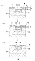
図3は、本発明の実施の形態の配線形成方法を工程順に示す。先ず、CMPまたは電解研磨により、基板Wの表面に成膜した余剰な銅(配線材料)16を研磨して除去し、これによって、図3(a)に示すように、トレンチ(配線用凹部)12内に埋込んだ銅16で配線18を形成するとともに、該配線形成部以外のバリア膜14を露出させる。つまり、銅16の表面を、バリア膜14を残して研磨除去し、トレンチ12内の配線18の表面がバリア膜14の表面とほぼ面一となるようにする。
なお、この余剰な銅16の除去を、無機酸または有機酸を用いたエッチングで行っても良い。
FIG. 3 shows the wiring forming method according to the embodiment of the present invention in the order of steps. First, excess copper (wiring material) 16 formed on the surface of the substrate W is polished and removed by CMP or electropolishing, whereby a trench (wiring recess) is formed as shown in FIG. A
The
このように、バリア膜14を残した状態で、このバリア膜14をマスクとした金属膜(保護膜)の成膜を行い、これによって、図3(b)に示すように、トレンチ12内の配線18の表面に、例えばコバルト合金やニッケル合金からなる金属膜(保護膜)20を選択的に成膜する。これによって、トレンチ12内の配線18の表面を金属膜20で覆って配線18を保護する。
In this way, with the
この金属膜20の成膜を、例えば無電解めっき、化学気相成長法(CVD)または物理気相成長法(PVD)で行う。この金属膜20の成膜を無電解めっきで行う場合には、トレンチ12内の配線18の表面に金属膜20が選択的に成膜するように、例えばPd等の触媒を付与する等の必要な前処理を行う。このめっき前処理は、前述の余剰な銅16の除去と同時に行うようにしてもよい。
The
そして、基板Wの表面にめっき液を接触させてめっきを行う。この時、基板Wの表面の配線形成部を除く領域は、一般に自然酸化膜で覆われて濡れ性が問題となることがないバリア膜14で覆われており、基板Wの表面の濡れ性を確保する必要はない。このため、絶縁膜10の材料の違いに拘わらず、同一のプロセス条件で配線18の表面にのみ金属膜20を選択的に成膜することができる。
Then, plating is performed by bringing the plating solution into contact with the surface of the substrate W. At this time, the region on the surface of the substrate W excluding the wiring forming portion is generally covered with a natural oxide film and covered with a
また、金属膜20の成膜を化学気相成長法で行う場合には、基板Wをチャンバ内に配置し、気相及び基板Wの表面での化学反応を利用して、トレンチ12内の配線18の表面に金属膜20を選択的に成長させる。この場合にあっても、基板Wの表面の配線形成部を除く領域はバリア膜14で覆われており、このバリア膜14がマスクとなって、バリア膜14の表面に金属膜が成膜されることが防止され、これによって、配線18の表面にのみ金属膜20を選択的に成膜することができる。
When the
次に、基板Wの表面に露出している絶縁膜10上のバリア膜14のみをCMPまたはエッチングにより選択的に除去し、これによって、図3(c)に示すように、表面を金属膜20で選択的に覆われて保護された銅からなる配線18の形成を完了させる。このように、金属膜20をマスクとして、バリア膜14のみを除去することで、機械的な要素の相対的な少ない方法でバリア膜14を除去することができる。つまり、配線18の表面に金属膜20が事前に形成されて該配線18が保護されているので、バリア膜14の除去方法として様々な方法を採用することができ、プロセス上の余裕が大きくなる。例えば、このバリア膜14の除去は、CMPによって行うことが実用的であるが、機械的な要素が化学的な要素に比較して相対的に少ないCMPで行うことができ、また電解研磨によって行ってもよい。更に、薬液によるエッチングやプラズマエッチングによって行うことで、機械的な要素によることなく、バリア膜を除去することができる。
Next, only the
湿式エッチングの場合には物理的な力がかからないので、銅やLow−k材膜のような脆弱な材料が存在してもダメージの懸念はない。しかしながらCMP法による場合には、荷重をかけて処理することになるので、ダメージを与えるおそれがある。そこでCMP法による場合は、化学反応性の強いスラリーを用い、低圧、低速で研磨することが必要である。また、電解研磨法であれば湿式エッチングと同様にほとんど荷重がかからないので、ダメージの懸念はない。 In the case of wet etching, no physical force is applied, so there is no fear of damage even if a fragile material such as copper or a low-k material film exists. However, in the case of the CMP method, processing is performed with a load, which may cause damage. Therefore, in the case of the CMP method, it is necessary to use a highly chemically reactive slurry and to polish at a low pressure and a low speed. Moreover, since the load is hardly applied like the wet etching if it is an electropolishing method, there is no fear of damage.
これにより、たとえ絶縁膜10がlow−k材のような機械的強度が極めて弱い材料からなる場合であっても、絶縁膜10に損傷を与えることなく、不要となったバリア膜14を確実に除去することができる。
しかも、金属膜の成膜選択性が不充分であって、バリア膜上に金属膜が多少成膜されたとしても、不要な金属膜をバリア膜ごと除去することにより、金属膜の十分な成膜選択性を確保することができる。
Thereby, even if the insulating
In addition, even if the metal film has insufficient film formation selectivity and a metal film is formed on the barrier film, the metal film can be sufficiently formed by removing the unnecessary metal film together with the barrier film. Membrane selectivity can be ensured.
図4は、本発明の他の実施の形態の配線形成方法を工程順に示す。先ず、CMP、電解研磨またはエッチングにより、基板Wの表面に成膜した余剰な銅(配線材料)16を研磨して除去し、これによって、図4(a)に示すように、トレンチ(配線用凹部)12内に埋込んだ銅16で配線18を形成するとともに、該配線形成部以外のバリア膜14を露出させる。この時、トレンチ12内の配線18の表面が露出するバリア膜14の表面とほぼ面一となった後、更に配線18の研磨またはエッチングを続けて、露出するバリア膜14の表面よりトレンチ12内に形成されるの配線18の表面の方が低くなるようにする。
FIG. 4 shows a wiring forming method according to another embodiment of the present invention in the order of steps. First, excess copper (wiring material) 16 formed on the surface of the substrate W is polished and removed by CMP, electropolishing or etching, whereby a trench (for wiring) is formed as shown in FIG. The
このバリア膜14の表面と配線18の表面との間の間隔Dは、バリア膜14の膜厚と、下記のように、配線18の表面に選択的に成膜される金属膜20の必要膜厚を勘案して決定され、バリア膜14の膜厚T1より大きく(D>T1)することが好ましい。また間隔Dは、バリア膜14の膜厚T1に、配線18の表面に形成される金属膜20の膜厚T2(図4(b)参照)を加えた厚みとほぼ等しく(D≒T1+T2)とすることが更に好ましい。例えば、バリア膜14の膜厚T1が10nmで、金属膜20の必要膜厚T2が10nmである場合には、バリア膜14の表面と配線18の表面との間の間隔Dを20nmとする。これにより、不要となったバリア膜14を除去した後の基板Wの表面に金属膜20が盛り上がってしまうことを防止して、基板Wの表面を平坦にすることができる。
The distance D between the surface of the
このように、バリア膜14を残した状態で、このバリア膜14をマスクとした金属膜(保護膜)の成膜を行い、これによって、図4(b)に示すように、トレンチ12内の配線18の表面に、例えばコバルト合金やニッケル合金からなる金属膜(保護膜)20を選択的に成膜する。これによって、トレンチ12内の配線18の表面を金属膜20で覆って配線18を保護する。
In this manner, a metal film (protective film) is formed using the
次に、基板Wの表面に露出している絶縁膜10上のバリア膜14のみをCMPまたはエッチングにより選択的に除去し、これによって、図4(c)に示すように、表面を金属膜20で選択的に覆われて保護された銅からなる配線18の形成を完了させる。この時、前述のように、不要な銅を除去した後のバリア膜14の表面と配線18の表面との間の間隔Dを、バリア膜14の膜厚T1に配線18の表面に形成される金属膜20の膜厚T2を加えた厚みとほぼ等しく(D≒T1+T2)することで、不要となったバリア膜14を除去した後の基板Wの表面を平坦にすることができる。
Next, only the
なお、不要な銅を除去した後のバリア膜14の表面と配線18の表面との間の間隔Dを、バリア膜14の膜厚T1に配線18の表面に形成される金属膜20の膜厚T2を加えた厚みより広く(D>T1+T2)するようにしてもよく、これにより、配線18の表面に金属膜20を形成した配線部分が、バリア膜14を除去した後、基板表面より突出することを防止することができる。
Note that the distance D between the surface of the
例えば、65nmノード世代以降の配線形成においては、基板表面の凹凸ができるだけ少ないことが求められる。従って、配線18上に成膜した金属膜20を、例えば信頼性向上のための密着層として使う場合にも、バリア膜14を除去した後の基板Wの表面上に、金属膜20が、例えば10nm以上盛り上がって存在することは好ましくない。この例によれば、不要となったバリア膜14を除去した後の基板Wの表面を平坦にするか、または配線部分が基板表面より突出することを防止することで、この要請に応えることができる。
For example, in wiring formation after the 65 nm node generation, it is required that the substrate surface has as few asperities as possible. Therefore, even when the
また、選択的に成膜した金属膜20をマスクとしてバリア膜14を除去する場合であっても、バリア膜14を除去後の絶縁膜10がなす平面から配線18が凸状に出ていることは同様に好ましくない。例えば、不要な銅を除去した後のバリア膜14の表面と配線18の表面との間の間隔Dを、バリア膜14の膜厚T1とほぼ等しくする(D≒T1)ことで、不要となったバリア膜14を除去した後の絶縁膜10がなす平面と、配線18の表面をほぼ面一にして、絶縁膜10がなす平面から配線18が凸状に出てしまうことを防止することができる。
Even when the
図5は、本発明の更に他の実施の形態の配線形成方法を工程順に示す。先ず、CMP、電解研磨またはエッチングにより、基板Wの表面に成膜した余剰な銅(配線材料)16を研磨して除去し、これによって、図5(a)に示すように、トレンチ(配線用凹部)12内に埋込んだ銅16で配線18を形成するとともに、該配線形成部以外のバリア膜14を露出させる。この時、この例では、トレンチ12内の配線18の表面が露出するバリア膜14の表面とほぼ面一となった後、更に配線18の研磨またはエッチングを続けて、露出するバリア膜14の表面よりトレンチ12内に形成されるの配線18の表面の方が低く、しかも、このバリア膜14の表面と配線18の表面との間の間隔D1が、バリア膜14の膜厚T1に、配線18の表面に形成される金属膜20の膜厚T2(図5(b)参照)を加え、更に絶縁膜10の除去代ΔT(図5(b)参照)を加えた厚さとほぼ等しく(D≒T1+T2+ΔT)なるようにする。例えば、バリア膜14の膜厚T1が10nm、金属膜20の必要膜厚T2が10nmである場合には、バリア膜14の表面と配線18の表面との間の間隔D1を20nmに絶縁膜10の除去代ΔTを加えた大きさにする。
FIG. 5 shows a wiring forming method according to still another embodiment of the present invention in the order of steps. First, excess copper (wiring material) 16 formed on the surface of the substrate W is polished and removed by CMP, electropolishing or etching, whereby a trench (for wiring) is formed as shown in FIG. The
このように、バリア膜14を残した状態で、このバリア膜14をマスクとした金属膜(保護膜)の成膜を行い、これによって、図5(b)に示すように、トレンチ12内の配線18の表面に、例えばコバルト合金やニッケル合金からなる金属膜(保護膜)20を選択的に成膜する。これによって、トレンチ12内の配線18の表面を金属膜20で覆って配線18を保護する。
In this way, with the
次に、基板Wの表面に露出している絶縁膜10上のバリア膜14をCMPまたはエッチングにより選択的に除去し、引き続いて、絶縁膜10の表面の一部を除去代ΔT分除去し、これによって、図5(c)に示すように、表面を金属膜20で選択的に覆われて保護された銅からなる配線18の形成を完了させる。このように、絶縁膜10上のバリア膜14を除去した後、絶縁膜10の表面を一部除去することで、絶縁膜10上のバリア膜14を完全に除去して、バリア膜14が絶縁膜10上に一部残ってしまうことを防止しすることができる。
Next, the
この時、前述のように、不要な銅を除去した後のバリア膜14の表面と配線18の表面との間の間隔D1を、バリア膜14の膜厚T1に配線18の表面に形成される金属膜20の膜厚T2を加え、更に絶縁膜10の除去代ΔTを加えた厚みとほぼ等しくすることで、不要となったバリア膜14及び絶縁膜10の表面の一部を除去代ΔT分除去した後の基板Wの表面を平坦にすることができる。
At this time, as described above, the distance D 1 between the surface of the
この絶縁膜10の表面の除去にあっても、配線18の表面に金属膜20が事前に形成されて該配線18が保護されているので、前述のバリア膜14と同様に、機械的な要素の相対的な少ない方法で除去することができる。例えば、薬液によるエッチングやプラズマエッチングによって、機械的な要素によることなく、絶縁膜10を除去することができる。
Even when the surface of the insulating
なお、不要な銅を除去した後のバリア膜14の表面と配線18の表面との間の間隔D1を、バリア膜14の膜厚T1に配線18の表面に形成される金属膜20の膜厚T2を加え、更に絶縁膜10の除去代ΔTを加えた厚みより大きく(D1>ΔT+T1+T2)することで、配線18の表面に金属膜20を形成した配線部分が、バリア膜14、更には絶縁膜10の表面の一部を除去した時に、基板表面より突出することを防止することができる。
また、図3及び図4に示す例にあっても、バリア膜14のエッチング等による除去に継続して、絶縁膜10の表面の一部をエッチング等で除去し、これによって、バリア膜14を絶縁膜10の表面から完全に除去するようにしてもよいことは勿論である。
Note that the distance D 1 between the surface of the
In the example shown in FIGS. 3 and 4, the
図6は、本発明の実施の形態の配線形成装置を示す平面配置図である。この配線形成装置は、ハウジング100内の床上のスペースの一端側に、一対の化学的機械的研磨(CMP)ユニット101、108が左右に対向して配置され、他端側にそれぞれ半導体ウエハ等の基板Wを収納するカセット102を載置するロード・アンロード部が配置されている。そして、研磨ユニット101とロード・アンロード部との間に、第1搬送ロボット103と第2搬送ロボット104が配置されている。更に、搬送ラインに沿った一方側には、ロールスポンジまたはペンシルスポンジを備えた第1洗浄ユニット105、第2洗浄(リンス・乾燥)ユニット106及び仮置台107が配置され、他方側には、保護膜形成用の第1前処理ユニット110と第2前処理ユニット111及び無電解めっきユニット112が配置されている。
FIG. 6 is a plan layout view showing the wiring forming apparatus according to the embodiment of the present invention. In this wiring forming apparatus, a pair of chemical mechanical polishing (CMP)
次に、この配線形成装置によって、図2の状態の基板Wを処理する一連の配線形成処理について、図3及び図6を参照して説明する。
まず、図2の状態の基板Wが収納されたカセット102から基板Wを1枚、第1搬送ロボット103で取り出し、仮置台107に搬送する。次いでこの基板Wを第2搬送ロボット104で取り上げ、研磨ユニット101へ搬入する。この研磨ユニット101で、トレンチ(配線用凹部)12の外の余剰な配線材料16を研磨して除去し、図3(a)に示すように、配線18を形成するとともに、バリア膜14を露出させる。この例では、図示しないが、研磨パッドを貼付して研磨面を構成する研磨テーブルに、トップリングで保持した基板Wの表面を所定圧力で押圧しつつ、研磨液(スラリー)を供給して研磨を行う。
次に、第2搬送ロボット104により、研磨後の基板Wを第1洗浄ユニット105に搬送して、例えば薬液とロールスポンジを用いて基板の表面を洗浄する。
Next, a series of wiring forming processes for processing the substrate W in the state of FIG. 2 by this wiring forming apparatus will be described with reference to FIGS.
First, one substrate W is taken out from the
Next, the polished substrate W is transferred to the
そして、この洗浄後の基板Wを第2搬送ロボット104で第1前処理ユニット110に搬送する。この第1前処理ユニット110では、めっき前処理としての基板表面の清浄化処理を行う。例えば、液温25℃の希釈H2SO4等の薬液を基板の表面全体に接触させ、銅等のCMP残さや、配線上の酸化物を除去し、しかる後、純水等のリンス液を用いてリンス(洗浄)する。
Then, the cleaned substrate W is transferred to the
次に、この洗浄後の基板Wを第2搬送ロボット104で第2前処理ユニット111に搬送する。この第2前処理ユニット111では、基板Wをフェースダウンで保持し、基板Wの表面に触媒付与処理を行う。例えば、保護膜(金属膜)成膜のための触媒金属を含む触媒液を基板Wの表面に向けて噴射し、配線18の表面を活性化させ、しかる後、基板Wの表面を純水等のリンス液を用いてリンス(洗浄)する。
Next, the cleaned substrate W is transferred to the
そして、この触媒を付与しリンス処理した基板Wを第2搬送ロボット104で無電解めっきユニット112に搬送し、この表面に無電解めっき処理を施し金属膜(保護膜)20を成膜する(図3(b)参照)。つまり、基板Wをフェースダウンで保持し、めっき槽に保持された無電解めっき液の液面へ降下させて、基板の表面をめっき液に接液させ、所定時間の後、基板をめっき液から引き上げ、pHが6〜7.5の中性液からなる停止液を基板Wの表面に接触させて、無電解めっき処理を停止させる。なお、図示しないが、第2前処理ユニット111と無電解めっきユニット112の間に、触媒付与後の基板Wの表面のpHの調整(中和処理)を行う第3前処理ユニットを設けてもよい。
Then, the substrate W that has been provided with the catalyst and rinsed is transported to the
次に、この金属膜を成膜した基板Wを第2搬送ロボット104で研磨ユニット108に搬送し、基板Wの表面の全体を研磨して不要なバリア膜14を除去する(図3(c)参照)。このとき、研磨液(スラリー)として金属膜(保護膜)よりもバリア膜に対して研磨レートの高い研磨液を用いるとよい。
Next, the substrate W on which the metal film is formed is transferred to the
そして、この研磨後の基板Wを第2搬送ロボット104で第1洗浄ユニット105に搬入し、界面活性剤、有機アルカリ、キレート剤等の薬品を含む薬液を供給ノズルから基板の表面に供給してロールスクラブ洗浄や、薬液のみによる洗浄をする。そして、このように薬液を使用した場合には、基板Wの表面に残った薬液を純水等のリンス液でリンスする。
Then, the polished substrate W is carried into the
この洗浄後の基板Wを第2搬送ロボット104で第2洗浄(リンス・乾燥)ユニット106へ搬入し、ここでリンス処理を行い、しかる後、基板Wを高速で回転させてスピン乾燥させる。この乾燥させた基板Wを第2搬送ロボット104で仮置台107へ搬送し、この基板を第1搬送ロボット103で取り上げ、カセット102へ搬入して、配線形成処理を完了する。
以上により、基板Wの表面に、金属膜(保護膜)20を持つ埋め込み配線を形成する一連の作業を連続して行うことができる。
The substrate W after the cleaning is carried into the second cleaning (rinsing / drying)
As described above, a series of operations for forming the embedded wiring having the metal film (protective film) 20 on the surface of the substrate W can be continuously performed.
図7は本発明の他の実施の形態の配線形成装置を示す平面配置図である。この配線形成装置は、ハウジング120を有し、このハウジング120の一端に基板Wを収納するカセット121を載置するロード・アンロード部が配置され、このロード・アンロード部からハウジング120の他端側に向かって、第1搬送ロボット122、仮置台125、第2搬送ロボット123、仮置台126及び第3搬送ロボット124が配置されている。第1搬送ロボット122は、仮置台125との間で基板Wの搬送を行い、第2搬送ロボットは、その周囲に配置された仮置台125、仮置台126、第1ウェットエッチングユニット127、第2ウェットエッチングユニット128、第1洗浄ユニット129及び第2洗浄ユニット130の間で基板Wの搬送を行う。第3搬送ロボット124は、仮置台126と、保護膜形成のための第1前処理ユニット131,131、第2前処理ユニット132,132及び無電解めっきユニット133,133との間で基板Wの搬送を行う。
FIG. 7 is a plan layout view showing a wiring forming apparatus according to another embodiment of the present invention. This wiring forming apparatus has a
この例によれば、図2の状態の基板Wが収納されたカセット121から基板Wを1枚、第1搬送ロボット122で取り出し、仮置台125に搬送する。次いでこの基板Wを第2搬送ロボット123で取り上げ、第1ウェットエッチングユニット127へ搬入する。この第1ウェットエッチングユニット127で、配線用凹部12の外の余剰な配線材料16を薬液によるエッチングにより除去して、図4(a)に示すように、配線18を形成するとともに、バリア膜14を露出させる。このとき、トレンチ12内に形成される配線18の表面が絶縁膜10の最上面よりも低くなるようにしてもよい。
According to this example, one substrate W is taken out from the
この基板Wを第2搬送ロボット123で第1洗浄ユニット129へ搬送し、ロールスクラブ洗浄等により基板の表面を洗浄した後、第2搬送ロボット123で仮置台126へ搬送する。基板の洗浄を1回としたが、処理条件によって、基板を第1洗浄ユニット129から第2洗浄ユニット130へ搬送して2段階の洗浄を行い、仮置台126へ送るようにしてもよい。
The substrate W is transported to the
この基板を第3搬送ロボット124により第1前処理ユニット131へ搬入し、めっき前処理としての基板表面の清浄化処理を行う。この基板を第3搬送ロボット124で第2前処理ユニット132、無電解めっきユニット133へ順次搬送し、無電解めっきを施して基板Wの配線18に、図4(b)のような金属膜(保護膜)20を形成する。この工程は、前述の例と同様である。基板表面のトレンチ12内に形成される配線18の表面が絶縁膜10の最上面よりも低い場合には、ここで形成する金属膜20の膜厚を、金属膜20の表面が絶縁膜10の最上面とほぼ同一面になるような膜厚にすることが好ましい。
The substrate is carried into the
さらに、無電解めっき処理の終了した基板Wを第3搬送ロボット124で仮置台126に載置した後、第2搬送ロボット123で第1洗浄ユニット129へ搬送して洗浄し、必要によっては、第2洗浄ユニット130で更に洗浄した後、第2ウェットエッチングユニット128に搬入する。第2ウェットエッチングユニット128では、基板Wの表面の全面にエッチング液を供給し、図4(c)に示すように、基板表面に絶縁膜10が露出するまでバリア膜14のエッチングを行う。
Further, after the electroless plating process is finished, the substrate W is placed on the temporary table 126 by the
しかる後、バリア膜14のエッチングが終了した基板Wを第1洗浄ユニット129へ搬送し、基板表面をロールスクラブ洗浄等によって洗浄し、この洗浄した基板Wを第2洗浄ユニット130へ搬送し、リンス処理を行った後、基板Wを高速で回転させてスピン乾燥させる。この乾燥させた基板Wを仮置台125へ載置し、第1搬送ロボット122によりカセット121へ収納して処理を完了する。
この装置によれば、脆弱な材料から構成される基板表面であっても、機械的なストレスをかけることなしに、保護膜20を持つ埋め込み配線を形成する一連の作業を連続して行うことができる。
Thereafter, the substrate W after the etching of the
According to this apparatus, a series of operations for forming embedded wiring having the
図8は本発明の更に他の実施の形態の配線形成装置を示す平面配置図である。この装置の構成は、ハウジング140内外に、先に図7に示したユニットの他に、第3搬送ロボット124がアクセスできる位置に研磨ユニット101が配置されている。
この装置によれば、本発明の配線形成方法を実施するにあたり、銅膜(配線材料)16の除去を研磨ユニット101で行い、無電解めっき処理の後、バリア膜14の除去をウェットエッチングユニット127または128で行うことができる。また、この装置による別の方法によれば、銅膜(配線材料)16の除去をウェットエッチングユニット127または128で行い、無電解めっき処理の後、バリア膜14の除去を研磨ユニット101で行うことができ、基板Wの表面を平坦に仕上げることができる。
FIG. 8 is a plan layout view showing a wiring forming apparatus according to still another embodiment of the present invention. In this apparatus, the polishing
According to this apparatus, when performing the wiring forming method of the present invention, the copper film (wiring material) 16 is removed by the polishing
10 絶縁膜
12 トレンチ(配線用凹部)
14 バリア膜
16 銅(配線材料)
18 配線
20 金属膜
101,108 化学的機械的研磨ユニット
102,121 カセット
105,106,129,130 洗浄ユニット
110,111,131,132 前処理ユニット
112,133 無電解めっきユニット
127,128 ウェットエッチングユニット
10 Insulating
14
18
Claims (15)
基板表面に成膜した余剰の前記配線材料を除去して前記配線用凹部内に埋込んだ配線材料で配線を形成するとともに、該配線形成部以外の前記バリア膜を露出させ、
前記配線の表面に金属膜を選択的に成膜することを特徴とする配線形成方法。 A barrier film is formed on the surface of the substrate in which the wiring recess is formed in the insulating film, and then a substrate in which the wiring material is formed in the wiring recess and on the substrate surface is prepared,
Excess wiring material formed on the substrate surface is removed to form wiring with the wiring material embedded in the wiring recess, and the barrier film other than the wiring forming portion is exposed,
A wiring forming method, wherein a metal film is selectively formed on a surface of the wiring.
基板を搬送する搬送ロボットと、
基板の表面全体を薬液でエッチングするウェットエッチングユニットと、
基板の表面に無電解めっきの前処理を施す前処理ユニットと、
基板の表面に無電解めっきを施す無電解めっきユニットと、
基板の表面を洗浄する洗浄ユニットとを有することを特徴とする配線形成装置。 A load / unload section for loading a cassette capable of storing substrates;
A transfer robot for transferring substrates;
A wet etching unit that etches the entire surface of the substrate with chemicals;
A pretreatment unit that performs pretreatment of electroless plating on the surface of the substrate;
An electroless plating unit for applying electroless plating to the surface of the substrate;
A wiring forming apparatus comprising a cleaning unit for cleaning a surface of a substrate.
Priority Applications (2)
| Application Number | Priority Date | Filing Date | Title |
|---|---|---|---|
| JP2004261247A JP2006041453A (en) | 2004-06-22 | 2004-09-08 | Method and apparatus for wiring formation |
| US10/941,882 US20050282378A1 (en) | 2004-06-22 | 2004-09-16 | Interconnects forming method and interconnects forming apparatus |
Applications Claiming Priority (2)
| Application Number | Priority Date | Filing Date | Title |
|---|---|---|---|
| JP2004184239 | 2004-06-22 | ||
| JP2004261247A JP2006041453A (en) | 2004-06-22 | 2004-09-08 | Method and apparatus for wiring formation |
Publications (2)
| Publication Number | Publication Date |
|---|---|
| JP2006041453A true JP2006041453A (en) | 2006-02-09 |
| JP2006041453A5 JP2006041453A5 (en) | 2007-07-19 |
Family
ID=35481169
Family Applications (1)
| Application Number | Title | Priority Date | Filing Date |
|---|---|---|---|
| JP2004261247A Withdrawn JP2006041453A (en) | 2004-06-22 | 2004-09-08 | Method and apparatus for wiring formation |
Country Status (2)
| Country | Link |
|---|---|
| US (1) | US20050282378A1 (en) |
| JP (1) | JP2006041453A (en) |
Cited By (4)
| Publication number | Priority date | Publication date | Assignee | Title |
|---|---|---|---|---|
| JP2008140880A (en) * | 2006-11-30 | 2008-06-19 | Tokyo Electron Ltd | Method of forming thin film, deposition apparatus and storage medium |
| JP2012146752A (en) * | 2011-01-07 | 2012-08-02 | Fujitsu Ltd | Semiconductor device and manufacturing method of the same |
| JP2014183127A (en) * | 2013-03-18 | 2014-09-29 | Fujitsu Ltd | Semiconductor device and manufacturing method of the same |
| JP2017188644A (en) * | 2016-03-31 | 2017-10-12 | 東京エレクトロン株式会社 | Formation method for hard mask, formation device for hard mask, and storage medium |
Families Citing this family (15)
| Publication number | Priority date | Publication date | Assignee | Title |
|---|---|---|---|---|
| US6764940B1 (en) | 2001-03-13 | 2004-07-20 | Novellus Systems, Inc. | Method for depositing a diffusion barrier for copper interconnect applications |
| US7842605B1 (en) | 2003-04-11 | 2010-11-30 | Novellus Systems, Inc. | Atomic layer profiling of diffusion barrier and metal seed layers |
| US8298933B2 (en) | 2003-04-11 | 2012-10-30 | Novellus Systems, Inc. | Conformal films on semiconductor substrates |
| US7727880B1 (en) | 2004-11-03 | 2010-06-01 | Novellus Systems, Inc. | Protective self-aligned buffer layers for damascene interconnects |
| US7727881B1 (en) | 2004-11-03 | 2010-06-01 | Novellus Systems, Inc. | Protective self-aligned buffer layers for damascene interconnects |
| US7510634B1 (en) | 2006-11-10 | 2009-03-31 | Novellus Systems, Inc. | Apparatus and methods for deposition and/or etch selectivity |
| US7682966B1 (en) | 2007-02-01 | 2010-03-23 | Novellus Systems, Inc. | Multistep method of depositing metal seed layers |
| US7932179B2 (en) * | 2007-07-27 | 2011-04-26 | Micron Technology, Inc. | Method for fabricating semiconductor device having backside redistribution layers |
| US20090032964A1 (en) * | 2007-07-31 | 2009-02-05 | Micron Technology, Inc. | System and method for providing semiconductor device features using a protective layer |
| US8268722B2 (en) * | 2009-06-03 | 2012-09-18 | Novellus Systems, Inc. | Interfacial capping layers for interconnects |
| US8524599B2 (en) | 2011-03-17 | 2013-09-03 | Micron Technology, Inc. | Methods of forming at least one conductive element and methods of forming a semiconductor structure |
| KR101995602B1 (en) | 2011-06-03 | 2019-07-02 | 노벨러스 시스템즈, 인코포레이티드 | Metal and silicon containing capping layers for interconnects |
| US9087777B2 (en) * | 2013-03-14 | 2015-07-21 | United Test And Assembly Center Ltd. | Semiconductor packages and methods of packaging semiconductor devices |
| US9633896B1 (en) | 2015-10-09 | 2017-04-25 | Lam Research Corporation | Methods for formation of low-k aluminum-containing etch stop films |
| US10224202B2 (en) * | 2016-03-31 | 2019-03-05 | Tokyo Electron Limited | Forming method of hard mask, forming apparatus of hard mask and recording medium |
Family Cites Families (7)
| Publication number | Priority date | Publication date | Assignee | Title |
|---|---|---|---|---|
| US5272104A (en) * | 1993-03-11 | 1993-12-21 | Harris Corporation | Bonded wafer process incorporating diamond insulator |
| US6303505B1 (en) * | 1998-07-09 | 2001-10-16 | Advanced Micro Devices, Inc. | Copper interconnect with improved electromigration resistance |
| US6153523A (en) * | 1998-12-09 | 2000-11-28 | Advanced Micro Devices, Inc. | Method of forming high density capping layers for copper interconnects with improved adhesion |
| US6046108A (en) * | 1999-06-25 | 2000-04-04 | Taiwan Semiconductor Manufacturing Company | Method for selective growth of Cu3 Ge or Cu5 Si for passivation of damascene copper structures and device manufactured thereby |
| US6611060B1 (en) * | 1999-10-04 | 2003-08-26 | Kabushiki Kaisha Toshiba | Semiconductor device having a damascene type wiring layer |
| US6716330B2 (en) * | 2000-10-26 | 2004-04-06 | Ebara Corporation | Electroless plating apparatus and method |
| US7193323B2 (en) * | 2003-11-18 | 2007-03-20 | International Business Machines Corporation | Electroplated CoWP composite structures as copper barrier layers |
-
2004
- 2004-09-08 JP JP2004261247A patent/JP2006041453A/en not_active Withdrawn
- 2004-09-16 US US10/941,882 patent/US20050282378A1/en not_active Abandoned
Cited By (4)
| Publication number | Priority date | Publication date | Assignee | Title |
|---|---|---|---|---|
| JP2008140880A (en) * | 2006-11-30 | 2008-06-19 | Tokyo Electron Ltd | Method of forming thin film, deposition apparatus and storage medium |
| JP2012146752A (en) * | 2011-01-07 | 2012-08-02 | Fujitsu Ltd | Semiconductor device and manufacturing method of the same |
| JP2014183127A (en) * | 2013-03-18 | 2014-09-29 | Fujitsu Ltd | Semiconductor device and manufacturing method of the same |
| JP2017188644A (en) * | 2016-03-31 | 2017-10-12 | 東京エレクトロン株式会社 | Formation method for hard mask, formation device for hard mask, and storage medium |
Also Published As
| Publication number | Publication date |
|---|---|
| US20050282378A1 (en) | 2005-12-22 |
Similar Documents
| Publication | Publication Date | Title |
|---|---|---|
| JP4644926B2 (en) | Semiconductor manufacturing apparatus and semiconductor device manufacturing method | |
| JP2006041453A (en) | Method and apparatus for wiring formation | |
| US8771804B2 (en) | Processes and systems for engineering a copper surface for selective metal deposition | |
| US8241701B2 (en) | Processes and systems for engineering a barrier surface for copper deposition | |
| TWI393186B (en) | Processes and integrated systems for engineering a substrate surface for metal deposition | |
| US10755934B2 (en) | Systems and methods for chemical mechanical polish and clean | |
| US8747960B2 (en) | Processes and systems for engineering a silicon-type surface for selective metal deposition to form a metal silicide | |
| KR101078627B1 (en) | Methods and systems for barrier layer surface passivation | |
| JP2006093357A (en) | Semiconductor device and manufacturing method thereof, and processing solution | |
| US20060003521A1 (en) | Method of and apparatus for manufacturing semiconductor device | |
| JP2006041453A5 (en) | ||
| US20060003570A1 (en) | Method and apparatus for electroless capping with vapor drying | |
| JP2006016684A (en) | Wiring method and wiring device | |
| JP2005044910A (en) | Method and device for forming wiring | |
| JP2003193246A (en) | Pretreatment method for electroless plating and pretreatment solution | |
| JP2008004615A (en) | Method and apparatus for forming wiring | |
| JP2005116630A (en) | Wiring forming method and apparatus thereof | |
| JP2006147655A (en) | Method of manufacturing semiconductor device | |
| JP2003034876A (en) | Catalytic treatment liquid and method for electroless plating | |
| JP2008072123A (en) | Forming method of electrically conductive pattern of semiconductor element | |
| JP2004363155A (en) | Method and device for manufacturing semiconductor device | |
| JP2005044913A (en) | Semiconductor device and manufacturing method thereof | |
| KR20010092109A (en) | Method for forming metal wire | |
| JP2007208142A (en) | Semiconductor device manufacturing method | |
| JP2003213438A (en) | Plating apparatus and plating method |
Legal Events
| Date | Code | Title | Description |
|---|---|---|---|
| A521 | Written amendment |
Free format text: JAPANESE INTERMEDIATE CODE: A523 Effective date: 20070606 |
|
| A621 | Written request for application examination |
Free format text: JAPANESE INTERMEDIATE CODE: A621 Effective date: 20070606 |
|
| A977 | Report on retrieval |
Free format text: JAPANESE INTERMEDIATE CODE: A971007 Effective date: 20090810 |
|
| A761 | Written withdrawal of application |
Free format text: JAPANESE INTERMEDIATE CODE: A761 Effective date: 20090812 |