JP2006040407A - Optical disk device - Google Patents
Optical disk device Download PDFInfo
- Publication number
- JP2006040407A JP2006040407A JP2004218729A JP2004218729A JP2006040407A JP 2006040407 A JP2006040407 A JP 2006040407A JP 2004218729 A JP2004218729 A JP 2004218729A JP 2004218729 A JP2004218729 A JP 2004218729A JP 2006040407 A JP2006040407 A JP 2006040407A
- Authority
- JP
- Japan
- Prior art keywords
- optical disk
- optical disc
- metal substrate
- turntable
- substrate
- Prior art date
- Legal status (The legal status is an assumption and is not a legal conclusion. Google has not performed a legal analysis and makes no representation as to the accuracy of the status listed.)
- Pending
Links
Images


Landscapes
- Optical Record Carriers And Manufacture Thereof (AREA)
- Holding Or Fastening Of Disk On Rotational Shaft (AREA)
Abstract
【課題】 ディスク基板にプラスチック材料を用いたために生じる帯電性により、光ディスクの記録または再生時に起こりやすい塵埃の付着しやすさと、これによって損なわれる再生能力を改善し、さらに、MDのようなマグネティック・クランプを採用したシステムにおいて、マグネティック・クランプの簡易化を可能にする。
【解決手段】 光ディスクの基板としてSUS430等の磁性を帯びやすい金属を使用する。また、光ディスク装置内の、光ディスクを載置するためのターンテーブルを磁石と一体形成することにより、光ディスクのマグネティック・クランプを容易に行う。また、上記光ディスクの記録または再生時にターンテーブルまたは位置決めのための軸を通してアースを取ることで、光ディスクに対する塵埃の付着を防ぐ。
【選択図】 図15PROBLEM TO BE SOLVED: To improve the ease of adhering dust which is likely to occur at the time of recording or reproduction of an optical disk and the reproduction ability impaired by the electrification generated by using a plastic material for a disk substrate. This makes it possible to simplify magnetic clamps in systems that use clamps.
As a substrate of an optical disk, a metal that is easily magnetized, such as SUS430, is used. In addition, the magnetic table can be easily magnetically clamped by integrally forming a turntable for mounting the optical disk in the optical disk apparatus with the magnet. Also, dust is prevented from adhering to the optical disk by grounding through a turntable or a positioning shaft during recording or reproduction of the optical disk.
[Selection] FIG.
Description
この発明は、静電気による塵埃の吸着を軽減できる光ディスク装置に関する。 The present invention relates to an optical disc apparatus capable of reducing dust adsorption due to static electricity.
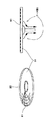
CD(Compact Disc)やDVD(Digital Versatile Disc)に代表される透明基板透過型の光ディスクメディアはポリカーボネート(以下、適宜PCと略す)、ポリメチルメタクリレート(以下、適宜PMMAと略す)、ガラスなどの透明基板を使うことが一般的である。その理由としては、図1に示すように、読み書き用のレーザ光14を透明基板11に透過させて、そのレンズ効果も活用しつつ絞り込んで透明基板11の奥に形成された信号層13に焦点を結ばせるためである。
Transparent substrate transmission type optical disc media represented by CD (Compact Disc) and DVD (Digital Versatile Disc) are transparent such as polycarbonate (hereinafter abbreviated as PC as appropriate), polymethyl methacrylate (hereinafter abbreviated as PMMA as appropriate), glass, and the like. It is common to use a substrate. The reason for this is that, as shown in FIG. 1, a
一方、昨今実用化されつつある、例えば図2に示すBlu−ray Disc(商品名、以下BDと適宜称する)に代表される高NA(Numerical Aperture)の光学系を用いた読み書き型の光ディスクメディアにおいては、基板の透過性は必要ではない。BDでは、カバーシート22とPSA(Pressure Sensitive Adhesive:感圧性接着剤)を用いた接着層23からなる0.1mm厚のカバー層24側からレーザ光26を入射させるため、基板21自体の透過性は問題とならないためである。
On the other hand, in a read / write optical disk medium using a high NA (Numerical Aperture) optical system represented by, for example, Blu-ray Disc (trade name, hereinafter referred to as BD as appropriate) shown in FIG. The substrate transparency is not necessary. In the BD, the
図1、図2に示すいずれの形状のディスクにおいても、信号層を複数設け、これを積層化することで容量を増やした多層光ディスクを作製できる。 In any of the disks shown in FIGS. 1 and 2, a multilayer optical disk having a plurality of signal layers and having a plurality of signal layers stacked to increase the capacity can be manufactured.
光ディスクの基板に不透明な材料を用いた場合の例として、以下の特許文献1、特許文献2および特許文献3が挙げられる。
Examples of the case where an opaque material is used for the substrate of the optical disk include the following Patent Document 1,
下記の特許文献1では、パーソナルコンピュータに標準搭載された光ディスク読み取り機において、データ転送速度の向上を目的にディスクの回転速度を上げた場合(回転数40,000rpm)、ディスクの表面が波打つなど、遠心応力に起因して発生する強度的な問題を解決するものである。 In the following Patent Document 1, when the rotation speed of a disk is increased for the purpose of improving the data transfer speed in an optical disk reader standardly installed in a personal computer (the rotation speed is 40,000 rpm), the surface of the disk is wavy, etc. This solves the strength problem caused by centrifugal stress.
特許文献1では、読み取り専用反射型光ディスクの基板をアルミニウム基合金、またはマグネシウム基合金のいずれか一方で構成することにより、回転の高速化によるデータ転送速度の向上が低コストで可能となるとともに、これまでプラスチックと金属の複合材料であり、資源リサイクルが困難であった読み取り専用反射型光ディスクのリサイクル性も向上させることができる。 In Patent Document 1, by configuring the substrate of the read-only reflective optical disk with either an aluminum-based alloy or a magnesium-based alloy, it is possible to improve the data transfer speed by increasing the rotation speed at a low cost, Recyclability of read-only reflective optical discs, which have been plastic and metal composite materials and have been difficult to recycle resources, can be improved.
また、特許文献2では、特許文献1に記載された読み取り専用反射型光ディスクにおける強度、リサイクル性と同様の特徴を有する書き込み可能反射型光ディスクに関するものである。
特許文献3では、光ディスクの強度を高め、耐摩耗性、耐衝撃性を向上させることを目的としている。光ディスクの高密度化のためにはピットを小さくする必要があるが、それに伴いピットを読み取る光スポット径も小さくする必要がある。このためには、レンズの開口数を大きくする方法を用いることが比較的容易であるが、この場合、光ディスクと光ヘッドをより近接させて制御しなければならない。
このため、光ディスクと光ヘッドが接触する恐れが生じ、光ディスクの耐摩耗性、耐衝撃性の向上が不可欠となる。そこで、特許文献3では、基板をアルミニウムまたはアルミニウム合金を用いて作製し、これらの課題を解決するものである。
For this reason, there is a risk of contact between the optical disk and the optical head, and it is essential to improve the wear resistance and impact resistance of the optical disk. Therefore, in
Blu−ray Discの基板としては、上述したように、CDやDVDで実用化されているPC、PMMAなどの透明プラスチックの表面に信号に対応する凹凸パターンを転写したものを用いることが一般的であるが、プラスチック材料は帯電しやすく、ディスクの作製工程や記録・再生中に塵埃がつきやすいという問題が生じ、これらのことが原因で再生能力が損なわれるおそれがある。 As described above, as a Blu-ray Disc substrate, it is common to use a substrate in which a concavo-convex pattern corresponding to a signal is transferred to the surface of a transparent plastic such as PC or PMMA that has been put to practical use in a CD or DVD. However, the plastic material is easily charged, and there arises a problem that dust is easily attached during the disc manufacturing process and recording / reproducing, and there is a possibility that the reproducing ability is impaired due to these.
さらに、MDのようなマグネティック・クランプを採用したシステムにおいては、鉄製のハブを別途用意し、これを基板に装着する必要がある。 Furthermore, in a system employing a magnetic clamp such as MD, it is necessary to prepare an iron hub separately and attach it to the substrate.
したがって、この発明の目的とするところは、ディスク基板にプラスチック材料を用いたために生じる帯電性により、光ディスクの記録または再生時に起こりやすい塵埃の付着しやすさと、これによって損なわれる再生能力を改善し、さらに、MDのようなマグネティック・クランプを採用したシステムにおいて、マグネティック・クランプの簡易化を可能にすることである。 Therefore, the object of the present invention is to improve the reproducibility that is impaired by the ease of adhesion of dust that tends to occur during recording or reproduction of the optical disk due to the charging property that is caused by using a plastic material for the disk substrate, Furthermore, in a system employing a magnetic clamp such as MD, it is possible to simplify the magnetic clamp.
上記課題を解決するために、この発明の第1の態様は、金属で構成された基板上に情報層を有し、情報層の上にカバー層を形成した光ディスクを記録または再生する光ディスク装置において、光ディスクの記録または再生時に金属基板を接地するようにした光ディスク装置である。 In order to solve the above-mentioned problems, a first aspect of the present invention is an optical disc apparatus that records or reproduces an optical disc having an information layer on a metal substrate and having a cover layer formed on the information layer. An optical disc apparatus in which a metal substrate is grounded during recording or reproduction of an optical disc.
この発明によれば、この金属基板が帯電しにくくなり、ディスク作成過程や再生装置を使って記録・再生動作中にディスク表面に塵埃を引き付けにくく、ディスク再生能力が安定する。 According to the present invention, this metal substrate is less likely to be charged, and it is difficult to attract dust to the disk surface during recording / reproducing operations using the disk making process or reproducing apparatus, and the disk reproducing ability is stabilized.
以下、この発明の一実施形態として、読取専用型の光ディスクを作製する工程を図面を参照しながら説明する。 Hereinafter, as an embodiment of the present invention, a process for producing a read-only optical disk will be described with reference to the drawings.
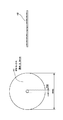
図3は、磁性を帯びやすい金属を用いて薄型円盤状(ディスク状)に加工した金属基板31の形状である。金属基板31は、例えば外形は直径50mm、中心孔直径2mm、厚み0.3mmとし、材料としては、例えばフェライト系ステンレスであるSUS430(JIS規格)等が用いられる。
FIG. 3 shows the shape of the
また、図4は金属基板31の表面に形成する凹凸信号のマスターとしてのプラスチック原盤41の一例である。プラスチック原盤41は、光ディスク基板の製造工程で一般的なNiスタンパを用いて、インジェクションモールディングによって形成された、厚さ0.3mm〜数mmの円盤である。材料はPMMAやPCなどの樹脂であるが、ゼオネックス(商品名:Zeonex 日本ゼオン社製)に代表される、紫外線硬化樹脂に対して剥離性に優れる環状ポリオレフィンなどが好ましい。大きさは金属基板31と同等もしくは金属基板31より大きいものがよい。
FIG. 4 shows an example of a
[ディスク基板作製工程]
次に、金属基板31に凹凸パターンを形成する。上述した金属基板31とプラスチック原盤41を対向させ、フォトポリマー法(2P法)によりプラスチック原盤41表面の凹凸信号を金属基板31に転写する。
[Disk substrate manufacturing process]
Next, an uneven pattern is formed on the
転写方法としては、プレスロール方式、真空圧着方式、スピンボンディング方式など、種々の方法が挙げられる。以下、図面を参照して各方法を説明する。 Examples of the transfer method include various methods such as a press roll method, a vacuum pressure bonding method, and a spin bonding method. Hereinafter, each method will be described with reference to the drawings.
図5は、プレスロール(Press−Roll)方式を説明する略線図である。金属基板31上に、あらかじめ決められたパターンで紫外線硬化樹脂を塗布した後、プラスチック原盤41の凹凸信号面を金属基板31側にして重ね、プレスロールにて貼り合わせる。その後、紫外線照射により樹脂を硬化させる。
FIG. 5 is a schematic diagram illustrating a press-roll system. An ultraviolet curable resin is applied in a predetermined pattern on the
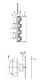
図6は、真空圧着転写方式(Pre−Coating&真空張り合わせ方式)を説明する略線図である。金属基板31の内周部にリング状に紫外線硬化樹脂を塗布し、スピンコーティングすることにより、平滑な樹脂膜を成膜した後、プラスチック原盤41の凹凸信号面を金属基板31側にして重ね、真空中で貼り合わせる。この時、プラスチック原盤41上から瞬時に押圧することにより、間に入った泡や隙間などを排除することが可能である。その後、プレスロール方式と同様に、紫外線照射により樹脂を硬化させる。
FIG. 6 is a schematic diagram illustrating a vacuum pressure bonding transfer method (Pre-Coating & vacuum bonding method). After applying a UV curable resin in a ring shape to the inner periphery of the
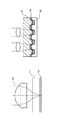
図7は、スピンボンディング(Spin−Bonding)方式を説明する略線図である。金属基板31の内周部にリング状に紫外線硬化樹脂を塗布し、プラスチック原盤41の内周部には多点状に紫外線硬化樹脂を塗布する。次に、プラスチック原盤41の凹凸信号面を金属基板31側にして重ね、貼り合わせる。貼り合せた金属基板31およびプラスチック原盤41をスピンさせ、紫外線硬化樹脂が均一に広がった後、紫外線照射により樹脂を硬化させる。
FIG. 7 is a schematic diagram illustrating a spin-bonding method. An ultraviolet curable resin is applied in a ring shape to the inner peripheral portion of the
図8は、図5〜図7で説明したプレスロール方式、真空圧着方式、スピンボンディング方式のいずれかにより金属基板31とプラスチック原盤41を貼り合せた後、金属基板31上に凹凸パターンが形成されるまでの流れを示す。
In FIG. 8, the
金属基板31とプラスチック原盤41を貼り合せた後、紫外線光をプラスチック原盤41側から照射して紫外線硬化樹脂を硬化させ、プラスチック原盤41を金属基板31上で硬化した樹脂から剥離することにより、金属基板31上に凹凸パターン81が転写されたディスク基板80が形成される。
After the
また、凹凸パターンの転写方法としては上述の方法のみに限ったものではなく、図9、図10に示す方法を用いてもよい。図9、図10に示す方法を、以下で説明する。 Further, the method for transferring the concavo-convex pattern is not limited to the above-described method, and the methods shown in FIGS. 9 and 10 may be used. The method shown in FIGS. 9 and 10 will be described below.
図9は、凹凸パターンをエンボス転写する方法を示している。半硬化の紫外線硬化型アシストPSA91をあらかじめ金属基板31にラミネート積層しておき、この表面に対してプラスチック原盤41の凹凸信号面を張り合わせ、紫外線を照射する。その後、プラスチック原盤41を剥離させることにより、紫外線硬化型アシストPSA91に凹凸パターンがエンボス転写され、ディスク基板が完成する。
FIG. 9 shows a method for embossed transfer of the concavo-convex pattern. A semi-cured UV
また、図10では、フォトリソグラフィーを用いた凹凸パターン転写方法を示している。上述の方法とは異なり、真空中で金属基板31自身にエッチングを施し、凹凸パターンを形成してディスク基板を作製するものである。
FIG. 10 shows an uneven pattern transfer method using photolithography. Unlike the method described above, the
この方法を用いた場合は金属基板1枚1枚にエッチングを施さなければならず、樹脂およびPSAを用いた場合と比較して時間、コストともに大きいものとなる。また、樹脂を用いた場合、金属基板に傷、へこみなどがあった場合でも樹脂の塗布により平滑化されるため、より正確な凹凸パターンの転写を行うことができることから、樹脂を用いるほうがより好適である。 When this method is used, each metal substrate must be etched, and both time and cost are increased compared to the case where resin and PSA are used. In addition, when a resin is used, even if there are scratches, dents, etc. on the metal substrate, it is smoothed by the application of the resin, so that a more accurate uneven pattern transfer can be performed. It is.
[金属基板型光ディスク作製工程]
次に、上述した方法により作製したディスク基板80を用いて金属基板型光ディスクを作製する。
[Metal substrate type optical disc manufacturing process]
Next, a metal substrate type optical disk is manufactured using the
図11に示すように、金属基板31上に形成された凹凸信号81上に、反射膜や記録膜を形成する。この膜は、Al反射膜、Ag反射膜、光磁気膜、金属相変化膜、有機色素膜、ホログラム膜など、光ディスクで一般的な膜で、その形成方法も真空蒸着、スパッタリング、スピンコーティング、ダイコーティング、ディップコーティング、スプレーコーティングなどが用いられるなど特に制約は無い。
As shown in FIG. 11, a reflective film or a recording film is formed on the
なお、この発明の金属基板型光ディスクでは、例えばスピンコートプロセス時、圧着プロセス、剥離プロセスにおける機台からもアースが取り易く、各工程で積極的にアース取りをすることで静電気による塵埃の吸着を軽減できる。 In the metal substrate type optical disc of the present invention, for example, it is easy to take the ground from the machine base in the spin coating process, the crimping process, and the peeling process, and the dust is adsorbed by static electricity by actively grounding in each process. Can be reduced.
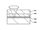
その後、読み取り側のカバー層114を形成する。例えばBDでは、0.1mmの透明プラスチックである。このカバー層114は、紫外線硬化樹脂をスピンコーティングによって形成したものや、PCなどの透明フィルムを接着剤や粘着剤を介して張り合わせた形態があるが、特に制約は無い。
Thereafter, the
以上の工程により、この発明の金属基板型光ディスクが形成される。 Through the above steps, the metal substrate type optical disk of the present invention is formed.
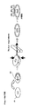
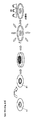
この金属基板型光ディスクを用いて記録・再生する際、金属基板を用いたことにより、クランピング方法としてマグネティック・クランプが有効に用いられる。例えば、図12に示すようにターンテーブル124の軸122の直径を2mm弱として、金属基板型光ディスク120をはめ込むことで位置決めを行う。この時、ターンテーブル124に埋蔵された磁石125がディスク基板120そのものを引き付け、同時にクランピングする。この場合、ターンテーブルの大きさは図12のように金属基板型光ディスクの外形より小さいものであっても問題ない。
When recording / reproducing using this metal substrate type optical disk, a magnetic clamp is effectively used as a clamping method by using the metal substrate. For example, as shown in FIG. 12, the diameter of the
ここで、ターンテーブルは磁石により一体形成したものまたは金属等を用いてテーブル形状を作製し、これに磁石を埋め込んだ構造であってもよい。ターンテーブル作製に用いる磁石としては、例えば、ボンド磁石、焼結磁石等が挙げられる。また、磁石の大きさ、磁力などは用途、目的に応じて最適なものに適宜調整すればよい。 Here, the turntable may have a structure in which a table is formed by using a magnet or a metal or the like, and a magnet is embedded in the turntable. Examples of the magnet used for producing the turntable include a bond magnet and a sintered magnet. Further, the size, magnetic force, etc. of the magnet may be appropriately adjusted to the optimum one according to the application and purpose.
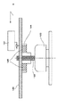
また、例えば、図13に示すような金属基板型光ディスクの外形にてセンタリングするタイプのもので、磁石を埋め込んだターンテーブル134を採用することにより、センターホールを有しないディスクも作製可能である。この場合、図14に示すように、センターホールによってデザイン等が欠けることがないため、デザインの幅が広がり、絵や文字を印刷したディスクメディアとすることもできる。
Further, for example, a disk that does not have a center hole can be manufactured by adopting a
金属基板型光ディスクの作製工程でも述べたように、この発明を適用した光ディスクでは、スピンコートプロセスや圧着プロセス、剥離プロセスにおける機台からもアースが取り易く、またそれのみならずドライブシステムのターンテーブルまたは回転軸からも容易にアースを取る事ができる。 As described in the manufacturing process of the metal substrate type optical disk, the optical disk to which the present invention is applied can easily be grounded from the machine base in the spin coating process, the pressure bonding process, and the peeling process, and not only the turntable of the drive system. Or it can be easily grounded from the rotating shaft.
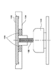
図15に示すように、基板が金属であるため、機台やターンテーブルを導電性の材料を用いて作製し、機台、ターンテーブル側でアースを取ることにより、静電気による塵埃の吸着を軽減することができる。 As shown in FIG. 15, since the substrate is made of metal, the machine base and turntable are made of a conductive material, and grounding is performed on the machine base and turntable side, thereby reducing dust adsorption due to static electricity. can do.
一例として、点線で示すように、[金属基板→ターンテーブル→回転軸→接地(例えばメカシャーシ)]の経路でアースを取ることができる。この場合、軸受けまたはブラシを使用して回転軸と接地との間の電気的接続を行うことができる。 As an example, as indicated by a dotted line, grounding can be performed through a path of [metal substrate → turn table → rotating shaft → grounding (for example, mechanical chassis)]. In this case, a bearing or brush can be used to make an electrical connection between the rotating shaft and ground.
以上、この発明の実施形態について具体的に説明したが、この発明は、上述の実施形態に限定されるものではなく、この発明の技術的思想に基づく各種の変形が可能である。 As mentioned above, although embodiment of this invention was described concretely, this invention is not limited to the above-mentioned embodiment, The various deformation | transformation based on the technical idea of this invention is possible.
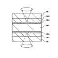
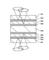
例えば、一実施形態として図16に示すような代表的な単層ディスクの例を示したが、この発明はこれにとどまらず、図17に示すように金属プレート両面に信号面を有する両面2層ディスク、また図18に示す片面2層ディスク、図19に示す片面2層を両面に有する4層ディスクなどの各多層ディスクにも適用可能である。 For example, an example of a typical single-layer disc as shown in FIG. 16 is shown as an embodiment, but the present invention is not limited to this, and double-sided two-layers having signal surfaces on both sides of a metal plate as shown in FIG. The present invention can also be applied to a multi-layer disc such as a disc, a single-sided dual-layer disc shown in FIG. 18, and a four-layer disc having two single-sided layers shown in FIG.
また、一実施形態として読取専用型の光ディスクの例を示したが、書き込み可能な光ディスクについても適用可能である。 Further, although an example of a read-only optical disc has been shown as an embodiment, the present invention can also be applied to a writable optical disc.
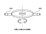
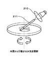
また、図20、21に示すように表面凹凸信号転写の際に紫外線照射の方向をプラスチック原盤からのみならず、内部エッジ部または外周エッジ部から照射して紫外線硬化樹脂を硬化させることもできる。 In addition, as shown in FIGS. 20 and 21, the ultraviolet curable resin can be cured by irradiating the direction of ultraviolet irradiation not only from the plastic master but also from the inner edge portion or the outer peripheral edge portion during the surface unevenness signal transfer.
11・・・透明基板
12、24、114・・・カバー層
13、25・・・信号層
31・・・金属基板
41・・・プラスチック原盤
42・・・凹凸信号
80・・・ディスク基板
81・・・転写凹凸信号
91、162・・・紫外線硬化型アシストPSA
101・・・クロムマスク
103・・・フォトレジスト
120・・・金属基板型光ディスク
122、132・・・軸
124、134・・・ターンテーブル
125、135・・・磁石
161・・・PCフィルム
163・・・信号層
164・・・金属基板
200・・・紫外線光
210・・・集光レンズ
211・・・光ファイバー
DESCRIPTION OF
DESCRIPTION OF
Claims (5)
上記光ディスクの記録または再生時に上記金属基板を接地するようにした光ディスク装置。 In an optical disc apparatus for recording or reproducing an optical disc having an information layer on a substrate made of metal and having a cover layer formed on the information layer,
An optical disc apparatus wherein the metal substrate is grounded during recording or reproduction of the optical disc.
上記光ディスク装置は、上記情報層が樹脂により形成された凹凸信号と、上記凹凸信号上に成膜された反射膜とからなる上記光ディスクを記録または再生する光ディスク装置。 The optical disk device according to claim 1,
The optical disk apparatus is an optical disk apparatus for recording or reproducing the optical disk comprising a concavo-convex signal in which the information layer is formed of a resin and a reflective film formed on the concavo-convex signal.
上記光ディスク装置は、上記情報層が記録可能な記録層である上記光ディスクを記録または再生する光ディスク装置。 The optical disk device according to claim 1,
The optical disc apparatus is an optical disc apparatus for recording or reproducing the optical disc, wherein the information layer is a recordable recording layer.
上記光ディスクを載置するターンテーブルの一部に磁石を配置し、上記光ディスクを上記ターンテーブルの回転軸を介して接地させることを特徴とする光ディスク装置。 The optical disk device according to claim 1,
An optical disc apparatus, wherein a magnet is disposed on a part of a turntable on which the optical disc is placed, and the optical disc is grounded via a rotation shaft of the turntable.
上記光ディスクを載置するターンテーブルの一部に磁石を配置し、上記光ディスクの外周を上記ターンテーブルの凹部によって位置決めし、上記光ディスクを上記ターンテーブルおよび回転軸を介して接地させることを特徴とする光ディスク装置。 The optical disk device according to claim 1,
A magnet is disposed on a part of a turntable on which the optical disc is placed, the outer periphery of the optical disc is positioned by a concave portion of the turntable, and the optical disc is grounded through the turntable and a rotating shaft. Optical disk device.
Priority Applications (1)
| Application Number | Priority Date | Filing Date | Title |
|---|---|---|---|
| JP2004218729A JP2006040407A (en) | 2004-07-27 | 2004-07-27 | Optical disk device |
Applications Claiming Priority (1)
| Application Number | Priority Date | Filing Date | Title |
|---|---|---|---|
| JP2004218729A JP2006040407A (en) | 2004-07-27 | 2004-07-27 | Optical disk device |
Publications (1)
| Publication Number | Publication Date |
|---|---|
| JP2006040407A true JP2006040407A (en) | 2006-02-09 |
Family
ID=35905237
Family Applications (1)
| Application Number | Title | Priority Date | Filing Date |
|---|---|---|---|
| JP2004218729A Pending JP2006040407A (en) | 2004-07-27 | 2004-07-27 | Optical disk device |
Country Status (1)
| Country | Link |
|---|---|
| JP (1) | JP2006040407A (en) |
Cited By (3)
| Publication number | Priority date | Publication date | Assignee | Title |
|---|---|---|---|---|
| WO2007094446A1 (en) | 2006-02-17 | 2007-08-23 | Toyo Ink Mfg. Co., Ltd. | Active energy ray-curable inkjet ink composition |
| WO2009044527A1 (en) * | 2007-10-04 | 2009-04-09 | Shibaura Mechatronics Corporation | Transfer apparatus |
| US9506618B2 (en) | 2012-12-25 | 2016-11-29 | Hon Hai Precision Industry Co., Ltd. | Automotive lamp system |
-
2004
- 2004-07-27 JP JP2004218729A patent/JP2006040407A/en active Pending
Cited By (4)
| Publication number | Priority date | Publication date | Assignee | Title |
|---|---|---|---|---|
| WO2007094446A1 (en) | 2006-02-17 | 2007-08-23 | Toyo Ink Mfg. Co., Ltd. | Active energy ray-curable inkjet ink composition |
| WO2009044527A1 (en) * | 2007-10-04 | 2009-04-09 | Shibaura Mechatronics Corporation | Transfer apparatus |
| JP4679664B2 (en) * | 2007-10-04 | 2011-04-27 | 芝浦メカトロニクス株式会社 | Transfer device |
| US9506618B2 (en) | 2012-12-25 | 2016-11-29 | Hon Hai Precision Industry Co., Ltd. | Automotive lamp system |
Similar Documents
| Publication | Publication Date | Title |
|---|---|---|
| US20040152501A1 (en) | Gaming machine and display device therefor | |
| JP2002260307A (en) | Method and apparatus for manufacturing optical information recording medium and optical information recording medium | |
| US7161893B2 (en) | Stamper for fabrication of optical recording medium, method of forming information recording area and light transmissive layer, and optical recording medium | |
| JP2003203402A (en) | Method for manufacturing optical information recording medium and optical information recording medium | |
| JP2006040407A (en) | Optical disk device | |
| JP4360269B2 (en) | Multilayer optical disc manufacturing method | |
| JPH0997452A (en) | Method for manufacturing multilayer optical recording medium | |
| JP2000036135A (en) | Method for manufacturing multilayer information recording medium | |
| JP4266044B2 (en) | Information recording medium | |
| JP4516414B2 (en) | Optical disc manufacturing method and optical disc | |
| JP3980992B2 (en) | Optical recording medium manufacturing method and optical recording medium | |
| US20050046689A1 (en) | Optical disk medium, optical disk medium production method, turntable and optical disk apparatus | |
| US20040158848A1 (en) | Optical disk and method for manufacturing the same | |
| WO2004036570A1 (en) | Optial information recording medium and production method therefor, production device | |
| EP1581942B1 (en) | Magnetically clamped optical disc and apparatus | |
| JP4433632B2 (en) | Manufacturing method of optical recording medium | |
| JP3086404B2 (en) | Single-sided playback composite optical disc structure | |
| JPH0917035A (en) | Composite optical disk structure and mold for manufacturing the same | |
| JP2007310994A (en) | Flexible optical disk and holder | |
| JP2007310998A (en) | optical disk | |
| JPH0963124A (en) | Composite optical disc structure | |
| JPH09306042A (en) | Method for manufacturing optical recording medium | |
| JP2004127380A (en) | Optical information recording medium | |
| JP2004126038A (en) | Optical information recording medium | |
| JP2002312982A (en) | Method of manufacturing optical recording medium and spindle device |
Legal Events
| Date | Code | Title | Description |
|---|---|---|---|
| RD04 | Notification of resignation of power of attorney |
Free format text: JAPANESE INTERMEDIATE CODE: A7424 Effective date: 20060209 |