JP2005534510A - Silicon (Si) or silicon germanium (SiGe) for MEMS applications with low temperature plasma - Google Patents
Silicon (Si) or silicon germanium (SiGe) for MEMS applications with low temperature plasma Download PDFInfo
- Publication number
- JP2005534510A JP2005534510A JP2004525975A JP2004525975A JP2005534510A JP 2005534510 A JP2005534510 A JP 2005534510A JP 2004525975 A JP2004525975 A JP 2004525975A JP 2004525975 A JP2004525975 A JP 2004525975A JP 2005534510 A JP2005534510 A JP 2005534510A
- Authority
- JP
- Japan
- Prior art keywords
- silicon
- layer
- mems
- temperature less
- forming
- Prior art date
- Legal status (The legal status is an assumption and is not a legal conclusion. Google has not performed a legal analysis and makes no representation as to the accuracy of the status listed.)
- Withdrawn
Links
Images


Classifications
-
- B—PERFORMING OPERATIONS; TRANSPORTING
- B81—MICROSTRUCTURAL TECHNOLOGY
- B81C—PROCESSES OR APPARATUS SPECIALLY ADAPTED FOR THE MANUFACTURE OR TREATMENT OF MICROSTRUCTURAL DEVICES OR SYSTEMS
- B81C1/00—Manufacture or treatment of devices or systems in or on a substrate
-
- B—PERFORMING OPERATIONS; TRANSPORTING
- B81—MICROSTRUCTURAL TECHNOLOGY
- B81C—PROCESSES OR APPARATUS SPECIALLY ADAPTED FOR THE MANUFACTURE OR TREATMENT OF MICROSTRUCTURAL DEVICES OR SYSTEMS
- B81C1/00—Manufacture or treatment of devices or systems in or on a substrate
- B81C1/00349—Creating layers of material on a substrate
- B81C1/0038—Processes for creating layers of materials not provided for in groups B81C1/00357 - B81C1/00373
-
- B—PERFORMING OPERATIONS; TRANSPORTING
- B81—MICROSTRUCTURAL TECHNOLOGY
- B81B—MICROSTRUCTURAL DEVICES OR SYSTEMS, e.g. MICROMECHANICAL DEVICES
- B81B3/00—Devices comprising flexible or deformable elements, e.g. comprising elastic tongues or membranes
-
- B—PERFORMING OPERATIONS; TRANSPORTING
- B81—MICROSTRUCTURAL TECHNOLOGY
- B81C—PROCESSES OR APPARATUS SPECIALLY ADAPTED FOR THE MANUFACTURE OR TREATMENT OF MICROSTRUCTURAL DEVICES OR SYSTEMS
- B81C1/00—Manufacture or treatment of devices or systems in or on a substrate
- B81C1/00015—Manufacture or treatment of devices or systems in or on a substrate for manufacturing microsystems
- B81C1/00222—Integrating an electronic processing unit with a micromechanical structure
- B81C1/00246—Monolithic integration, i.e. micromechanical structure and electronic processing unit are integrated on the same substrate
-
- H—ELECTRICITY
- H01—ELECTRIC ELEMENTS
- H01G—CAPACITORS; CAPACITORS, RECTIFIERS, DETECTORS, SWITCHING DEVICES OR LIGHT-SENSITIVE DEVICES, OF THE ELECTROLYTIC TYPE
- H01G5/00—Capacitors in which the capacitance is varied by mechanical means, e.g. by turning a shaft; Processes of their manufacture
- H01G5/16—Capacitors in which the capacitance is varied by mechanical means, e.g. by turning a shaft; Processes of their manufacture using variation of distance between electrodes
- H01G5/18—Capacitors in which the capacitance is varied by mechanical means, e.g. by turning a shaft; Processes of their manufacture using variation of distance between electrodes due to change in inclination, e.g. by flexing, by spiral wrapping
-
- B—PERFORMING OPERATIONS; TRANSPORTING
- B81—MICROSTRUCTURAL TECHNOLOGY
- B81B—MICROSTRUCTURAL DEVICES OR SYSTEMS, e.g. MICROMECHANICAL DEVICES
- B81B2201/00—Specific applications of microelectromechanical systems
- B81B2201/01—Switches
- B81B2201/012—Switches characterised by the shape
- B81B2201/018—Switches not provided for in B81B2201/014 - B81B2201/016
-
- B—PERFORMING OPERATIONS; TRANSPORTING
- B81—MICROSTRUCTURAL TECHNOLOGY
- B81B—MICROSTRUCTURAL DEVICES OR SYSTEMS, e.g. MICROMECHANICAL DEVICES
- B81B2201/00—Specific applications of microelectromechanical systems
- B81B2201/02—Sensors
- B81B2201/0292—Sensors not provided for in B81B2201/0207 - B81B2201/0285
-
- B—PERFORMING OPERATIONS; TRANSPORTING
- B81—MICROSTRUCTURAL TECHNOLOGY
- B81C—PROCESSES OR APPARATUS SPECIALLY ADAPTED FOR THE MANUFACTURE OR TREATMENT OF MICROSTRUCTURAL DEVICES OR SYSTEMS
- B81C2201/00—Manufacture or treatment of microstructural devices or systems
- B81C2201/01—Manufacture or treatment of microstructural devices or systems in or on a substrate
- B81C2201/0161—Controlling physical properties of the material
- B81C2201/0163—Controlling internal stress of deposited layers
- B81C2201/0164—Controlling internal stress of deposited layers by doping the layer
-
- B—PERFORMING OPERATIONS; TRANSPORTING
- B81—MICROSTRUCTURAL TECHNOLOGY
- B81C—PROCESSES OR APPARATUS SPECIALLY ADAPTED FOR THE MANUFACTURE OR TREATMENT OF MICROSTRUCTURAL DEVICES OR SYSTEMS
- B81C2203/00—Forming microstructural systems
- B81C2203/07—Integrating an electronic processing unit with a micromechanical structure
- B81C2203/0707—Monolithic integration, i.e. the electronic processing unit is formed on or in the same substrate as the micromechanical structure
- B81C2203/0735—Post-CMOS, i.e. forming the micromechanical structure after the CMOS circuit
Abstract
MEMS構造(69)の形成方法が提供される。この方法によれば、その上に堆積した配線金属(53)を有するCMOS基板(51)を設ける。MEMS構造は基板の上に、シリコン及びシリコン−ゲルマニウム合金から成るグループから選択される材料をプラズマ化学気相成長(PACVD)を使用して堆積させることにより形成される。PACVDの使用に付随する低成長温度によって、これらの材料を、CMOS集積化プロセスの後工程におけるMEMS形成に使用することが可能になる。A method of forming a MEMS structure (69) is provided. According to this method, a CMOS substrate (51) having a wiring metal (53) deposited thereon is provided. The MEMS structure is formed on a substrate by depositing a material selected from the group consisting of silicon and silicon-germanium alloy using plasma enhanced chemical vapor deposition (PACVD). The low growth temperatures associated with the use of PACVD allow these materials to be used for MEMS formation later in the CMOS integration process.
Description
本発明は概してMEMSデバイスに関し、より詳細には、MEMSデバイスをシリコン及びシリコンゲルマニウム合金から作製するための低温プラズマ法に関する。 The present invention relates generally to MEMS devices, and more particularly to a low temperature plasma method for making MEMS devices from silicon and silicon germanium alloys.
マイクロマシン技術及び他のマイクロ加工技術、及びプロセスの進歩によって多種多様な微小電気機械システム(Micro Electro Mechanical Systems: MEMS)及びMEMSデバイスの形成が可能になっている。これらのシステム及びデバイスは、可動ロータ、ギア、スイッチ、加速度計、小型センサ、アクチュエータシステムなどの構造を含む。 Advances in micromachine technology and other microfabrication technologies and processes have made it possible to form a wide variety of micro electro mechanical systems (MEMS) and MEMS devices. These systems and devices include structures such as movable rotors, gears, switches, accelerometers, miniature sensors, actuator systems, and the like.
マイクロ加工の一の重要な用途はRF MEMSスイッチの形成である。このようなデバイスは、これらのデバイスと対比されるべき固体の等価物よりも優れる幾つかの利点を有する。例えば、RF MEMSスイッチは固体スイッチよりも低い挿入損失、良好な絶縁性、良好な直線性、及び低い電力を示す。RF MEMSデバイスはまた、種々の用途において有用である。従って、これらのデバイスは調整可能なプリセレクタ及び周波数シンセサイザとして使用することができ、そして信号ルーティングデバイス、インピーダンス整合ネットワーク、及び調整可能な利得増幅器を含む種々の電気通信デバイス及びシステムの構成要素として有用でもある。 One important application of micromachining is the formation of RF MEMS switches. Such devices have several advantages over the solid equivalents to be contrasted with these devices. For example, RF MEMS switches exhibit lower insertion loss, better insulation, better linearity, and lower power than solid state switches. RF MEMS devices are also useful in a variety of applications. Thus, these devices can be used as adjustable preselectors and frequency synthesizers and are useful as components in various telecommunications devices and systems, including signal routing devices, impedance matching networks, and adjustable gain amplifiers. But there is.
図1,2(図2は図1の側面図である)は、従来のRF MEMSスイッチ10を示している。スイッチはカンチレバーアーム20を備え、このアームは通常、絶縁材料からなり、かつ基板12にアンカー構造14によって取り付けられる。アンカー構造は、堆積による積層、又は周囲材料の選択除去、或いは選択エッチング除去によって基板上にメサとして形成することができる。通常は接地される下部電極16、及び信号ライン18も基板上に形成される。下部電極及び信号ラインは通常、容易には酸化されない金など金属から成る細片からなる。信号ラインと下部電極との間には間隙がある。
1 and 2 (FIG. 2 is a side view of FIG. 1) show a conventional
スイッチの作動部は上述のカンチレバーアーム20を備える。カンチレバーアームは懸架マイクロビームを形成し、このマイクロビームはその一端がアンカー構造の最上部に取り付けられ、そして基板上に配置される下部電極及び信号ラインの上方を覆って延在する。電気コンタクト22も通常、容易には酸化されない金などの金属からなり、アンカー構造から離れたカンチレバーアームの端部の上に形成される。電気コンタクトはカンチレバーアームの底面側に位置して信号ラインの上方を覆う形で基板の最上部に面している。
The switch operating portion includes the above-described
通常、アルミニウム又は金などの金属を含む上部電極24はカンチレバーアームの上に形成される。上部電極はアンカー構造の上方の位置を起点としてカンチレバーアームの最上部に沿って下部電極の上方の位置の端部にまで延びる。カンチレバーアーム及び上部電極は下部電極(この電極自体が広がっている)の上方に広がっていてキャパシタ構造26を形成する。キャパシタ構造には格子状の穴が設けられてこの構造の質量を減らしている。
Typically, the
動作状態では、スイッチは普通、図2に示すように「オフ」ポジションになっている。スイッチがオフ状態になると、信号ラインは、電気コンタクトと信号ラインとの間に間隙が介在することによってオープン回路になる。スイッチは、電圧を上部電極に印加することにより作動して「オン」ポジションになる。上部電極に電圧が印加されると、静電気力によってキャパシタ構造(及びカンチレバーアーム)が下部電極の方に引き付けられる。
矢印11で示すようにカンチレバーアームが下部電極に向かって移動することにより、電気コンタクトが信号ラインに当接する方向に移動するのでギャップが無くなって信号ラインがオン状態となる(すなわち回路を閉じる)。
In the operating state, the switch is normally in the “off” position as shown in FIG. When the switch is turned off, the signal line becomes an open circuit due to a gap between the electrical contact and the signal line. The switch is activated by applying a voltage to the upper electrode to the “on” position. When a voltage is applied to the upper electrode, the capacitor structure (and cantilever arm) is attracted toward the lower electrode by electrostatic force.
As the cantilever arm moves toward the lower electrode as indicated by an arrow 11, the electrical contact moves in a direction in contact with the signal line, so that there is no gap and the signal line is turned on (ie, the circuit is closed).
図1,2に示すタイプのデバイスに生じる一つの問題は、デバイスの幾つかの構成部品に使用される材料の間に観察される熱膨張係数(CTE)の不一致に関するものである。特にRF MEMSスイッチの場合、熱的不一致は通常、上部電極(上述のように通常、Auのような金属から作製される)とカンチレバーアーム(普通、酸窒化シリコン(SiON)のような材料から作製される)との間に生じる。その結果、スイッチの可動部が、離脱の後のパッケージングプロセス期間中に生じる熱サイクル期間中に恒久的に歪んでしまうので、スイッチの動作特性に変化が生じ、そして多くの場合、スイッチが故障する。 One problem that arises with devices of the type shown in FIGS. 1 and 2 is related to the coefficient of thermal expansion (CTE) discrepancy observed between the materials used in several components of the device. Especially for RF MEMS switches, the thermal mismatch is usually made from a material such as a top electrode (usually made from a metal like Au as described above) and a cantilever arm (usually silicon oxynitride (SiON)). To occur). As a result, the moving parts of the switch are permanently distorted during the thermal cycle that occurs during the packaging process after release, resulting in a change in the operating characteristics of the switch and, in many cases, failure of the switch. To do.
他の種々の材料がMEMS形成プロセスに使用されてきており、これらの材料の内の幾つかは、SiONのCTE(熱膨張係数)に更に一致する方向の値のCTEを有する。しかしながら、これらの材料の多くをRF MEMSスイッチの上部電極に使用する手法は、従来の形成方法に付随する処理を考慮に入れると用いられることがなかった。従って、例えばシリコン及びシリコン/ゲルマニウム合金がLPCVDを使用するMEMSプロセスにおける構造素子として使用されてきており、しかも多くの所望特性を示している。しかしながら、通常のRF MEMSスイッチの最高処理温度は約350℃に制限され(主として犠牲層が設けられることに起因するが、この犠牲層は通常、ポリイミド又は同様な感熱材料から作製される)、LPCVDプロセス又はエピタキシャルプロセスにおけるシリコン又はシリコン−ゲルマニウム合金に必要な約550℃の堆積温度よりもかなり低い。 Various other materials have been used in the MEMS formation process, some of these materials have values of CTE that more closely match the CTE (Coefficient of Thermal Expansion) of SiON. However, the technique of using many of these materials for the upper electrode of the RF MEMS switch has not been used in view of the processing associated with conventional formation methods. Thus, for example, silicon and silicon / germanium alloys have been used as structural elements in MEMS processes using LPCVD and have exhibited many desirable properties. However, the maximum processing temperature of a typical RF MEMS switch is limited to about 350 ° C. (mainly due to the provision of a sacrificial layer, which is usually made from polyimide or a similar thermal material) and LPCVD. Much lower than the deposition temperature of about 550 ° C. required for silicon or silicon-germanium alloys in process or epitaxial processes.
処理温度を考慮に入れると、他のMEMS用途におけるシリコン及びシリコン/ゲルマニウム合金のような材料が所望の物理及び電気特性を示すにも拘らず、これらの材料も同様に、用いることができなかった。このような用途においては、例えばCMOS(相補型金属酸化膜半導体)構造と共に集積化される、センサ及びアクチュエータのようなMEMSデバイスが形成される。CMOS構造は、この構造が電力消費及び電力損失が小さく、更にはオフ状態での電流が最小になることから、デジタル機能を実行するために非常に有効なデバイス構成である。CMOSと両立し得る実用レベルのマイクロマシン技術を用いることにより、微細構造及びサポート回路を一緒に同じ基板の上に設けることができるので、集積化プロセスで形成することができる。 Taking into account the processing temperature, materials such as silicon and silicon / germanium alloys in other MEMS applications could not be used as well, although materials such as silicon and silicon / germanium alloys exhibited the desired physical and electrical properties. . In such applications, MEMS devices such as sensors and actuators are formed that are integrated with, for example, CMOS (complementary metal oxide semiconductor) structures. The CMOS structure is a very effective device configuration for performing digital functions because this structure has low power consumption and power loss, and further minimizes current in the off state. By using a micromachine technology at a practical level compatible with CMOS, the microstructure and the support circuit can be provided together on the same substrate, and thus can be formed by an integration process.
しかしながら、CMOSプロセスへの適切な統合、及びCMOSの各世代間の円滑な遷移を確実に行なうためには、MEMS形成をCMOSプロセスの後工程に組み入れることが好適である。このためには、配線金属を既に堆積させた後にMEMS構造を形成することが必要である。しかしながら、配線金属が基板の上に在ると、基板を450℃超の温度に晒さないようにする必要があり、これらの温度はこの場合もやはり、LPCVD又はエピタキシャルプロセスにおけるシリコン又はシリコン−ゲルマニウム合金に必要な約550℃の堆積温度よりもかなり低い。従って、これらの材料をCMOSデバイスの後工程における処理に使用することができない。幾つかのプロセスフローではこの問題を、MEMS形成をCMOSプロセスの最初又は中間に組み入れることにより回避することが可能であるが、このようにすると、CMOSの各世代間の円滑なプロセス遷移に制約を与えてしまうので望ましくない。 However, in order to ensure proper integration into the CMOS process and smooth transitions between each generation of CMOS, it is preferable to incorporate MEMS formation into the post-process of the CMOS process. For this purpose, it is necessary to form the MEMS structure after the wiring metal has already been deposited. However, if wiring metal is on the substrate, it is necessary to avoid exposing the substrate to temperatures above 450 ° C., which again is silicon or silicon-germanium alloys in LPCVD or epitaxial processes. Considerably lower than the deposition temperature of about 550 ° C. required for the process. Therefore, these materials cannot be used for processing in the subsequent process of the CMOS device. In some process flows this problem can be avoided by incorporating MEMS formation at the beginning or middle of the CMOS process, but this limits smooth process transitions between CMOS generations. Because it gives, it is not desirable.
従って、この技術分野においては、MEMSデバイス又はMEMSデバイスの構成要素をシリコン又はシリコン−ゲルマニウム合金から低温で形成する方法が必要となる。また
、この技術分野においては、CMOSプロセスの後工程に組み入れることができ、かつセンサ及びアクチュエータの形成に使用することができるこれらの材料に基づいてMEMS構造又はMEMS構成要素を形成する方法が必要となる。さらに、この技術分野においては、上部電極及びカンチレバーアームのCTE(熱膨張係数)がほぼ一致するRF CMOSデバイス及びその形成方法が必要となる。これらの要求及び他の要求は本明細書に開示するデバイス及び方法によって満たされる。
Accordingly, there is a need in the art for a method of forming MEMS devices or components of MEMS devices from silicon or silicon-germanium alloys at low temperatures. There is also a need in the art for a method of forming a MEMS structure or MEMS component based on these materials that can be incorporated into subsequent processes of a CMOS process and used to form sensors and actuators. Become. Further, in this technical field, there is a need for an RF CMOS device and a method of forming the same, in which the CTE (coefficient of thermal expansion) of the upper electrode and the cantilever arm are substantially the same. These and other needs are met by the devices and methods disclosed herein.
一の態様では、MEMSデバイスの形成方法が本明細書において提供される。この方法によれば、基板を設け、そしてMEM構造又はMEM構造の構成部品を基板の上に、シリコン及びシリコン−ゲルマニウム合金から成るグループから選択される材料をプラズマ化学気相成長(PACVD)を使用して堆積させることにより形成する。PACVDによる低温によって、これらの材料を、処理を考慮に入れるとこれらの材料を今までは使用できなかった形成プロセスに使用することができ、さらにこれらの材料にその場で不純物をドープすることができる。この方法によれば、PACVDを使用してMEMS構造(又はMEMS構造の構成部品)を種々の基板の上に、さらに種々の用途において形成することができる。従って、例えばPACVDを使用してMEMS構造をCMOS基板の上に形成することができる(この場合、MEMS構造は、例えばセンサ又はアクチュエータとすることができる)。PACVDを使用してMEMS構造又は構成部品(例えば、電極及び構造素子を含む)をRF MEMS形成プロセスで形成することもできる。 In one aspect, a method for forming a MEMS device is provided herein. According to this method, a substrate is provided, and a material selected from the group consisting of silicon and a silicon-germanium alloy is used by plasma enhanced chemical vapor deposition (PACVD) on the substrate with a MEM structure or a component of the MEM structure. Then, it is formed by depositing. Due to the low temperature by PACVD, these materials can be used in forming processes that could not be used before when processing is taken into account, and these materials can be doped in situ with impurities. it can. According to this method, a MEMS structure (or a component part of the MEMS structure) can be formed on various substrates using PACVD in various applications. Thus, for example, PACVD can be used to form a MEMS structure on a CMOS substrate (in this case, the MEMS structure can be, for example, a sensor or an actuator). PACVD can also be used to form MEMS structures or components (eg, including electrodes and structural elements) with an RF MEMS formation process.
別の態様では、MEMS構造の形成方法が提供される。この方法によれば、配線金属をその上に堆積させたCMOS基板を設ける。配線金属は、例えば金又はアルミニウムからなるものであってもよい。MEMS構造又はその構成部品を基板の上に、シリコン及びシリコン−ゲルマニウム合金から成るグループから選択される材料をプラズマ化学気相成長を使用して堆積させることにより形成する。プラズマ化学気相成長(PACVD)は通常、約450℃未満、好適には約400℃未満、更に好適には約350℃未満、更に好適には約300℃未満、そして最適には約250℃未満の温度で生じる。必要に応じて、材料には、この材料が堆積している間に不純物をドープすることができる。 In another aspect, a method for forming a MEMS structure is provided. According to this method, a CMOS substrate having a wiring metal deposited thereon is provided. The wiring metal may be made of, for example, gold or aluminum. A MEMS structure or component thereof is formed on a substrate by depositing a material selected from the group consisting of silicon and a silicon-germanium alloy using plasma enhanced chemical vapor deposition. Plasma enhanced chemical vapor deposition (PACVD) is typically less than about 450 ° C, preferably less than about 400 ° C, more preferably less than about 350 ° C, more preferably less than about 300 ° C, and optimally less than about 250 ° C. Occurs at temperatures of If desired, the material can be doped with impurities while the material is being deposited.
更に別の態様では、超小型電気機械センサ及びアクチュエータの形成方法が本明細書において提供される。この方法によれば、その上に少なくとも第1表面領域及び第2表面領域を有するCMOS基板を設け、第1表面領域がシリコン、ガラス、及び砒化ガリウムから成るグループから選択される第1材料を含み、第2表面領域が酸化シリコン及びポリイミドから成るグループから選択される第2材料を含む。第3材料から成る層は基板を覆うように形成され、さらに第1及び第2領域の少なくとも一部を覆って延び、第3材料がシリコン及びシリコン−ゲルマニウム合金から成るグループから選択され、そして第3材料から成る層が約450℃未満、好適には約350℃未満、更に好適には約300℃未満、そして最適には約250℃未満の温度でプラズマ化学気相成長プロセスを使用して形成される。第2材料の少なくとも一部を第3材料から成る層の下方から除去することにより第3材料を含む超小型機械変形素子を形成する。 In yet another aspect, a method for forming a microelectromechanical sensor and actuator is provided herein. According to this method, a CMOS substrate having at least a first surface region and a second surface region is provided thereon, and the first surface region includes a first material selected from the group consisting of silicon, glass, and gallium arsenide. The second surface region comprises a second material selected from the group consisting of silicon oxide and polyimide. The third material layer is formed to cover the substrate, further extends over at least a portion of the first and second regions, the third material is selected from the group consisting of silicon and a silicon-germanium alloy, and A layer of three materials is formed using a plasma chemical vapor deposition process at a temperature below about 450 ° C., preferably below about 350 ° C., more preferably below about 300 ° C., and optimally below about 250 ° C. Is done. By removing at least a part of the second material from below the layer made of the third material, a micromechanical deformation element including the third material is formed.
更に別の態様では、RF MEMSスイッチの形成方法が本明細書において提供される。この方法によれば、その上に画定される信号ライン又は他の回路を有し、RF MEMSスイッチを支持する基板を設ける。犠牲層を基板の少なくとも一部に設ける。次に、RF MEMSスイッチの構造素子を犠牲層を覆うように形成し、そして上部電極を構造素子の上にプラズマ化学気相成長プロセスを使用して形成する。上部電極は通常、約400℃未満、好適には約350℃未満、更に好適には約300℃未満、そして最適には約250℃未満の温度で形成される。上部電極はシリコン及びシリコン−ゲルマニウム合金から成るグループから選択される材料を含む。次に、犠牲層の少なくとも一部を構造素子の下
方から除去することにより構造素子を切り離す。
In yet another aspect, a method for forming an RF MEMS switch is provided herein. According to this method, a substrate is provided having a signal line or other circuit defined thereon and supporting an RF MEMS switch. A sacrificial layer is provided on at least part of the substrate. Next, a structural element of the RF MEMS switch is formed over the sacrificial layer, and an upper electrode is formed on the structural element using a plasma enhanced chemical vapor deposition process. The top electrode is typically formed at a temperature of less than about 400 ° C, preferably less than about 350 ° C, more preferably less than about 300 ° C, and optimally less than about 250 ° C. The top electrode includes a material selected from the group consisting of silicon and silicon-germanium alloys. Next, the structural element is separated by removing at least part of the sacrificial layer from below the structural element.
別の態様では、RF MEMSスイッチが提供され、このスイッチはシリコン及びシリコン/ゲルマニウム合金から成るグループから選択される材料を含む。スイッチは好適にはカンチレバーアームを備え、及び好適には電極がカンチレバーアームの最上部の上に設けられる。第2電極は好適にはカンチレバーアームの下方に配置される。 In another aspect, an RF MEMS switch is provided, the switch comprising a material selected from the group consisting of silicon and a silicon / germanium alloy. The switch preferably comprises a cantilever arm, and preferably an electrode is provided on the top of the cantilever arm. The second electrode is preferably disposed below the cantilever arm.
更に別の態様では、上述の方法を使用して形成することができるデバイスが開示される。
これらの態様及び他の態様について以下に更に詳細に記載する。
In yet another aspect, a device that can be formed using the methods described above is disclosed.
These and other aspects are described in further detail below.
化学気相成長(CVD)は、膜、コーティング及び構造をガス前駆体から形成するためにこの技術分野では広く使用されている。例えば、低圧化学気相成長(LPCVD)を含む幾つかの異なる種類のCVDが現在知られている。 Chemical vapor deposition (CVD) is widely used in the art to form films, coatings and structures from gas precursors. For example, several different types of CVD are currently known, including low pressure chemical vapor deposition (LPCVD).
つい最近開発された種類のCVDはプラズマ化学気相成長(PACVD)であり、PECVDとも呼ばれる。PACVDでは、コーティング材料を生成する前駆体の反応を誘起するエネルギーはプラズマイオン及び電子が前駆体と衝突することにより生じる。プラズマ自体は通常、マイクロ波又は電界を使用することにより生成される。PACVDは前駆体を熱によって反応させる現象を利用する訳ではないので、PACVDプロセスにおいて基板が晒される温度は、LPCVD又はエピタキシーのような他の普通に使用される堆積プロセスにおいて基板が晒される温度よりも低い場合が多い。 The most recently developed type of CVD is plasma enhanced chemical vapor deposition (PACVD), also called PECVD. In PACVD, the energy that induces the reaction of the precursor that produces the coating material is generated by the collision of plasma ions and electrons with the precursor. The plasma itself is usually generated by using microwaves or electric fields. Since PACVD does not make use of the phenomenon of precursor reaction by heat, the temperature at which the substrate is exposed in the PACVD process is higher than the temperature at which the substrate is exposed in other commonly used deposition processes such as LPCVD or epitaxy. Are often low.
現在では、PACVDをシリコン又はシリコン/ゲルマニウム合金用のMEMS形成プロセスに上手く使用してこのようなプロセスにおいて基板が晒される温度を相当に低減することができることが判明している。特に、PACVDを使用すると、シリコン及びシリコン/ゲルマニウム合金を、LPCVD又はエピタキシーに基づくMEMS形成プロセスにおいてこれらの材料に通常必要とされる約550℃の堆積温度に比べて200〜300℃の範囲という低温で堆積させることができる。これにより、シリコン及びシリコン/ゲルマニウム合金に基づくMEMSデバイス及びその構成部品(アンカー部分、マイクロビーム、カンチレバーアーム、及び他のMEMS構造及び部品を含む)を、温度上の制約から従来の形成方法(LPCVDプロセス又はエピタキシープロセスのような)では使用することができない種々の基板の上に形成することができる。従って、例えばPACVDを使用してRF MEMSスイッチの上に電極(上部電極を含む)を形成することができる。PACVDを使用して加速度計、圧力センサ、及びこれらのデバイスの構成部品をCMOS基板の上に形成することもでき、この場合、PACVDにより可能になる低温によってPACVDを集積化プロセスの後工程で使用することができる。 It has now been found that PACVD can be successfully used in MEMS forming processes for silicon or silicon / germanium alloys to significantly reduce the temperature to which the substrate is exposed in such processes. In particular, using PACVD, silicon and silicon / germanium alloys can be used at temperatures as low as 200-300 ° C. compared to the deposition temperature of about 550 ° C. typically required for these materials in LPCVD or epitaxy based MEMS formation processes. Can be deposited. This allows MEMS devices and their components (including anchor portions, microbeams, cantilever arms, and other MEMS structures and components) based on silicon and silicon / germanium alloys to be fabricated in a conventional manner (LPCVD) due to temperature constraints. It can be formed on a variety of substrates that cannot be used (such as processes or epitaxy processes). Thus, for example, PACVD can be used to form electrodes (including the top electrode) on top of the RF MEMS switch. PACVD can also be used to form accelerometers, pressure sensors, and component parts of these devices on a CMOS substrate, in which case PACVD is used later in the integration process due to the low temperatures enabled by PACVD. can do.
本明細書における示唆に従ってMEMS構造及び構成部品を形成するために使用するのに適するPACVD反応装置を図3に示す。この図に示すように、反応装置31は反応チャンバー33から成り、このチャンバー内に基板35を置く。反応チャンバーはポンプ37によってほぼ真空状態に維持される。基板は、反応チャンバー内で適切な成長温度に基板ヒータ39を使用して維持される。基板の温度は熱電対41によってモニターされる。本明細書において記載される用途では、基板は通常、約450℃未満、好適には約350℃未満、更に好適には約300℃未満、最適には約250℃未満の温度に維持される。
A PACVD reactor suitable for use in forming MEMS structures and components in accordance with the suggestions herein is shown in FIG. As shown in this figure, the
PACVD反応装置は前駆体ガスを分解して材料を基板の上に堆積させる。例えば、シラン(SiH4)を前駆体ガスとしてシリコンの堆積に使用することができる。前駆体ガスは、反応チャンバーと開放連通しているガス容器43に供給される。前駆体ガスのガス
容器への流入はガスマニホールド45により一定量に制御される。前駆体ガスが反応チャンバーに流入すると、これらのガスはRF電極47によって生成されるプラズマと反応し、そして分解反応してシリコン及び他の固体反応生成物を生成し、これらの材料が基板の上に膜として堆積する。
The PACVD reactor decomposes the precursor gas and deposits material on the substrate. For example, silane (SiH 4 ) can be used for silicon deposition as a precursor gas. The precursor gas is supplied to a
PACVDによって低成長温度が可能になるのに加えて、PACVDがMEMS形成に関連する他の成長方法よりも遥かに優れる点は、不純物ドープがその場で行なわれる、すなわち材料が堆積している最中に材料に不純物がドープされる、ということである。これは、適切なガスをPACVDのガス供給流に導入することにより行なうことができ、このガスが堆積チャンバー内で分解反応して適切な不純物を生成することができる。従って、例えばn型不純物をドープしたい場合にはホスフィン(PH3)を供給流に導入し、そしてp型不純物をドープしたい場合にはジボラン(B2H6)を導入することができる。これらのガスは分解されて基本となるリン及びボロンをそれぞれ生成し、これらのリン及びボロンが、形成中の層に導入される。これとは対照的に、従来の手法では多くの場合、層又は構造が形成された後に層又は構造に不純物をドープする必要がある。このような堆積後の不純物ドープを行なうと基板が損傷し、そして不純物分布に好適でない勾配も生じる。 In addition to allowing low growth temperatures with PACVD, PACVD is far superior to other growth methods associated with MEMS formation because impurity doping is performed in-situ, ie when the material is deposited. The material is doped with impurities. This can be done by introducing a suitable gas into the PACVD gas feed stream, which can decompose and produce suitable impurities in the deposition chamber. Thus, for example, phosphine (PH 3 ) can be introduced into the feed stream if it is desired to dope n-type impurities, and diborane (B 2 H 6 ) can be introduced if it is desired to dope p-type impurities. These gases are decomposed to produce basic phosphorus and boron, respectively, which are introduced into the layer being formed. In contrast, conventional approaches often require doping a layer or structure after the layer or structure has been formed. Such post-deposition impurity doping results in damage to the substrate and an unfavorable gradient in impurity distribution.
一旦、不純物が構造材料に導入されると、不純物が種々の手段により活性化される。PACVDプロセス自体で或る程度の不純物活性化が生じる。しかしながら、不純物の完全な活性化は他の種々の手段によって行なわれる。レーザアニールは不純物の完全活性化に特に望ましい方法である、というのは、完全活性化が基板を高温に晒すことなく行なわれるからである。 Once the impurities are introduced into the structural material, the impurities are activated by various means. Some degree of impurity activation occurs in the PACVD process itself. However, complete activation of the impurities is accomplished by various other means. Laser annealing is a particularly desirable method for full activation of impurities because full activation is performed without exposing the substrate to high temperatures.
図4〜15は1つの可能な形成手順を示しており、このシーケンスにより、本明細書が示唆するRF MEMSを形成することができる。このプロセスにより形成される構造は、その構成が図1,2に示す先行技術構造とは異なるが、同じ普通の方法を使用して図1,2に示す構造と同様な構造で、上部金属電極をシリコン電極に置き換えた構造を形成することもできることを理解されたい。 4-15 illustrate one possible formation procedure, this sequence can form an RF MEMS as suggested herein. The structure formed by this process is similar to the structure shown in FIGS. 1 and 2 using the same conventional method, although the structure is different from the prior art structure shown in FIGS. It should be understood that a structure can be formed in which is replaced with a silicon electrode.
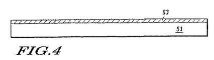
図4に示すように、高抵抗率シリコン、酸化シリコン、又はGaAsなどの材料からなる基板51を設ける。SiO2から成る層53を基板の上に、例えば熱酸化によって、通常約0.8ミクロンの厚さに堆積させる。図5に示すように、次に、RF MEMSスイッチ(例えば、信号を入力する/出力するために、そして/又は接地を行なうために)を支持する金属配線55を酸化シリコン層の上に画定させるが、この画定は、第1フォトマスク(図示せず)を酸化シリコン層を覆うように形成し、その後蒸着及びリフトオフを行なうことにより行なわれる。次に、ポリイミドスペーサ57を図6に示すように形成する。
As shown in FIG. 4, a
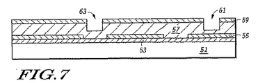
次に、第1SiONエッチングマスク59をPACVDによりポリイミド層を覆うように形成し、その後、構造にリセス(窪み)を画定するための第2フォトマスク(図示せず)を形成する。次に、コンタクトリセス61及びコンタクトポストリセス63を、犠牲材料(ポリイミド)中を構造内に一部の深さにまで達するエッチングにより形成し、その後、リセスマスクを除去して図7に示す構造を形成する。
Next, a first
図8に示すように、第2SiONエッチングマスク65をPACVDにより第1SiONエッチングマスクを覆うように形成する。第3フォトマスク(図示せず)を構造を覆うように形成し、そして適切なエッチング技術を使用し、層57を貫通するエッチングを行なうことによりアンカービアリセス67を構造中に画定する。次に図9に示すように、第1及び第2SiONマスクを構造から除去する。
As shown in FIG. 8, a second
図10に示すように、移動止め69及び短絡バー71をそれぞれコンタクトリセス及びコンタクトポストリセスに形成するが、これらの移動止め及び短絡バーは、第4フォトマスク(図示せず)を形成し、その後蒸着及びリフトオフを行なうことにより構造中に予め画定させておいたものである。図11に示すように、次に、デバイスのカンチレバー部分73を構成する部分又は層をPACVDにより低応力SiONから形成する。図12に示すように、次に例えばシリコン又はシリコン/ゲルマニウム合金を含むパターニング済み上部電極75をカンチレバーアームの上に、第5フォトマスク(図示せず)を形成し、その後蒸着及びリフトオフを行なうことにより形成する。この場合、上部電極を形成するためにPACVDを使用すると有利である、というのは、PACVDにより低温処理が可能になるだけでなく、シリコン又はシリコン/ゲルマニウム合金にその場で不純物をドープすることができるという利点があるからである。
As shown in FIG. 10, a
図13に示すように、多くのエッチング孔77をSiON層に、第6フォトマスク(図示せず)を使用し、その後エッチングを行なうことにより形成する、或いは選択エッチングにより形成する。開口79をアンカービアリセスの底面に同様な方法で画定させて下敷き金属配線を露出させる。
As shown in FIG. 13, many etching holes 77 are formed in the SiON layer by using a sixth photomask (not shown) and then performing etching, or by selective etching. An
図14に示すように、アンカーパッド81をアンカービアリセスに、第7フォトマスク(図示せず)を形成し、その後蒸着及びリフトオフを行なうことにより形成する。結果として得られるアンカーパッドは上部電極75とボンディングパッド55との間の電気接続を形成する。次に図15に示すように、最終構造83を、ポリイミド層57を薬品によって除去することにより切り離す。
As shown in FIG. 14, an
本明細書における示唆に従ってシリコン膜又はシリコン−ゲルマニウム膜を形成するために使用するPACVDプロセスのパラメータを調整して結果として得られる膜の結晶性を変えることができる。例えば、パルスガス導入方式を採用して、RF MEMS及び他の種々のMEMSデバイスに使用するナノ結晶PACVDシリコン膜を形成することができる。このようなナノ結晶膜は、その場で不純物をドープして低抵抗率の膜を形成する幾つかのプロセスにおいて特に有利である。 The parameters of the PACVD process used to form the silicon film or silicon-germanium film can be adjusted in accordance with the suggestions herein to change the crystallinity of the resulting film. For example, a pulse gas introduction method can be employed to form a nanocrystalline PACVD silicon film for use in RF MEMS and other various MEMS devices. Such nanocrystalline films are particularly advantageous in some processes in which impurities are doped in situ to form low resistivity films.
本明細書において記載するデバイス及び方法に関する理解は、本発明を制限するものではない次の実施例を参照することにより更に深めることができる。
(実施例1〜42)
これらの実施例では、PACVDを使用してシリコンを基板の上に低温成長させることができる。
An understanding of the devices and methods described herein can be further enhanced by reference to the following examples, which do not limit the invention.
(Examples 1-42)
In these embodiments, PACVD can be used to grow silicon on the substrate at a low temperature.
一連のシリコンウェハ基板を、ノベラス コンセプト ワン プラズマCVD装置(サンノゼ(米国カリフォルニア州)に本拠を置くノベラスシステムズ社による市販製品を利用できる)の反応チャンバーに置く。このシステムには真空ポンプ及びガス流入口が設けられ、ガス流入口は、シランが前駆体として、そしてヘリウムがキャリアガスとして安定に流れるように適合させている。システムには、反応チャンバー内の温度を安定に維持する温度制御機構、及び調整可能な電力出力を有するマイクロ波電源も設けられる。前駆体及びキャリアガスの流量、マイクロ波電源のワット量、及び各実験に関する反応チャンバーの温度及び圧力は表1に示す通りである。 A series of silicon wafer substrates are placed in the reaction chamber of a Novellus Concept One Plasma CVD system (available from Novellus Systems, Inc., based in San Jose, Calif., USA). The system is provided with a vacuum pump and a gas inlet, the gas inlet adapted to stably flow silane as a precursor and helium as a carrier gas. The system is also provided with a temperature control mechanism that maintains a stable temperature in the reaction chamber and a microwave power source with adjustable power output. The flow rates of the precursor and carrier gas, the wattage of the microwave power source, and the reaction chamber temperature and pressure for each experiment are as shown in Table 1.

表1に示すデータから分かるように、堆積プロセスの諸パラメータを350℃を超えない温度範囲(RF MEMSスイッチの最大温度範囲)で変えて約160オングストローム/分〜約1000オングストローム/分で変化する堆積速度を実現することができる。
堆積させるシリコンの膜厚は、約700オングストローム〜約3500オングストローム超で変化し、そして形成した層は低い残留応力を有する。これらの堆積速度及び膜厚は実用的なMEMS形成プロセスに対して十分なレベルのものである。
As can be seen from the data shown in Table 1, deposition process parameters are varied from about 160 angstroms / minute to about 1000 angstroms / minute with the temperature range not exceeding 350 ° C. (maximum temperature range of the RF MEMS switch). Speed can be realized.
The film thickness of the deposited silicon varies from about 700 angstroms to over about 3500 angstroms, and the formed layer has low residual stress. These deposition rates and film thicknesses are sufficient for a practical MEMS formation process.
堆積速度に対して温度、圧力、及びRF電力が及ぼす効果という観点から、表1のデータから或るトレンドを認めることもできる。これらのトレンドを理解し易くするために、表1から選択されるデータポイントを図16,17にグラフで示す。ここで、図16は堆積速度を温度の関数(圧力を2Torrとする)として示し、そしてRF電力が200ワット及び400ワットの場合のデータポイントを含んでいる。図16に示すように、RF電力が堆積速度に大きく影響することが分かり、この場合、電力が大きくなると所与の温度における堆積速度が大きくなる。温度は、電力ほどではないが、所与のRF電力での堆積速度に顕著に影響することがわかる。 Certain trends can also be observed from the data in Table 1 in terms of the effects of temperature, pressure, and RF power on the deposition rate. To facilitate understanding of these trends, the data points selected from Table 1 are shown graphically in FIGS. Here, FIG. 16 shows the deposition rate as a function of temperature (with a pressure of 2 Torr) and includes data points for RF powers of 200 and 400 watts. As shown in FIG. 16, it can be seen that the RF power greatly affects the deposition rate, where the deposition rate at a given temperature increases as the power increases. It can be seen that temperature is not as great as power but significantly affects the deposition rate at a given RF power.
図17は、温度が350℃のときの反応チャンバーにおける堆積速度を圧力の関数として表わすグラフである。このグラフから分かるように、堆積速度はテスト対象範囲の圧力に対して直線的に変化する。 FIG. 17 is a graph representing the deposition rate in the reaction chamber as a function of pressure when the temperature is 350 ° C. As can be seen from this graph, the deposition rate varies linearly with the pressure in the test area.
表1のデータを再度参照すると、堆積層のSi−H結合の実効量から、シランを前駆体として使用するシリコン成長用のPACVDを使用してアモルファス水素化シリコン層を形成することが可能であることが分かる。アモルファス水素化シリコンは、処理の施されていないアモルファスシリコンの材料特性よりもはるかに良好な材料特性を有する、というのは、後者の欠陥密度が前者の欠陥密度よりも高く、かつこれらの欠陥が作用して捕捉電荷キャリアが容易に再結合するからである。従って、PACVDをMEMS形成に使用すると、プロセスによって可能になる低温からもたらされる利点よりも大きな利点がもたらされることが分かる。 Referring back to the data in Table 1, from the effective amount of Si—H bonds in the deposited layer, it is possible to form an amorphous hydrogenated silicon layer using PACVD for silicon growth using silane as a precursor. I understand that. Amorphous silicon hydride has material properties that are much better than those of untreated amorphous silicon, because the latter defect density is higher than the former defect density and these defects are This is because the trapped charge carriers easily recombine by acting. Thus, it can be seen that the use of PACVD for MEMS formation provides a greater advantage than the low temperature enabled by the process.
これらの結果から、PACVDを使用してMEMS形成プロセスにおいてシリコンを実用的に達成できる速度で、かつ実現可能な膜厚に堆積させることができることが分かる。さらに、基板がこのプロセスにおいて晒される温度が十分に低いのでPACVDをRF MEMSスイッチの形成に、又はMEMS構造の形成に、後工程を含む従来のCMOSプロセスのどの時点でも使用することができる。また、PACVDプロセスによって堆積するシリコンの物理特性は、電気特性の点で他の幾つかの方法により形成されるシリコン層よりも優れる。
(比較例1)
この比較例は、固体の上部金電極を有する形で作製されるスイッチの熱特性を示している。図15に示すタイプで、図4〜15に示す一般的な方法に従って形成されるスイッチを形成するが、上部電極が固体の金であり、かつ0.2ミクロンの厚さを有する点が異なる。金電極の弾性率及び熱膨張係数を求め(60〜80℃の範囲の温度で)、そして表2に示す。
(実施例43〜45)
次の実施例は、PACVDにより形成したRF MEMSの熱安定性を示している。
These results show that PACVD can be used to deposit silicon at a rate that can be achieved practically and in a feasible film thickness in the MEMS formation process. Furthermore, since the temperature at which the substrate is exposed in this process is sufficiently low, PACVD can be used at any point in the conventional CMOS process, including post processing, to form RF MEMS switches or to form MEMS structures. Also, the physical properties of silicon deposited by the PACVD process are superior to silicon layers formed by some other methods in terms of electrical properties.
(Comparative Example 1)
This comparative example shows the thermal characteristics of a switch made with a solid top gold electrode. The type shown in FIG. 15 forms a switch formed according to the general method shown in FIGS. 4-15 except that the top electrode is solid gold and has a thickness of 0.2 microns. The elastic modulus and thermal expansion coefficient of the gold electrode were determined (at temperatures in the range of 60-80 ° C.) and are shown in Table 2.
(Examples 43 to 45)
The following example shows the thermal stability of RF MEMS formed by PACVD.
実施例43では、スイッチを比較例1と同じように形成するが、金電極を0.3ミクロン厚さのアンドープシリコン電極で置き換える点が異なる。電極の弾性率及び熱膨張係数を再度求め、そして表2に示す。 In Example 43, the switch is formed in the same manner as in Comparative Example 1, except that the gold electrode is replaced with an undoped silicon electrode having a thickness of 0.3 microns. The elastic modulus and thermal expansion coefficient of the electrode were again determined and are shown in Table 2.
実施例44では、スイッチを比較例1と同じように形成するが、金電極を0.3ミクロン厚さを有し、ボロンをドープしたシリコン電極で置き換える点が異なる。電極の弾性率
及び熱膨張係数を再度求め、そして表2に示す。
In Example 44, the switch is formed in the same manner as in Comparative Example 1, except that the gold electrode is replaced with a silicon electrode having a thickness of 0.3 microns and doped with boron. The elastic modulus and thermal expansion coefficient of the electrode were again determined and are shown in Table 2.
実施例45では、スイッチを比較例1と同じように形成するが、金電極を0.3ミクロン厚さを有し、リンをドープしたシリコン電極で置き換える点が異なる。電極の弾性率及び熱膨張係数を再度求め、そして表2に示す。 In Example 45, the switch is formed in the same manner as in Comparative Example 1, except that the gold electrode is replaced with a silicon electrode having a thickness of 0.3 microns and doped with phosphorus. The elastic modulus and thermal expansion coefficient of the electrode were again determined and are shown in Table 2.
表2の結果から分かるように、実施例43〜45のスイッチの上の上部電極は金電極の熱膨張係数よりもずっと小さい熱膨張係数を有するので、実施例43〜45のスイッチの熱安定性が、比較例1のスイッチに比べて改善されていることが示される。実施例43〜45のスイッチの上の上部電極はかなり大きな弾性率も有するので、比較例1のスイッチの電極に比べて感度がかなり低くなっている。しかしながら、これらのパラメータ(弾性率及び感度)の両方がほとんどの用途における許容範囲に収まるので、これらの結果を最適化する必要は全くない。 As can be seen from the results in Table 2, the upper electrode above the switches of Examples 43-45 has a coefficient of thermal expansion much smaller than that of the gold electrode, so the thermal stability of the switches of Examples 43-45. Is shown to be improved compared to the switch of Comparative Example 1. Since the upper electrode on the switches of Examples 43 to 45 also has a considerably large elastic modulus, the sensitivity is considerably lower than that of the electrode of the switch of Comparative Example 1. However, since both of these parameters (modulus and sensitivity) are acceptable for most applications, there is no need to optimize these results.
図18は、シリコンを金の替わりに図12に示すタイプのスイッチに使用するときの作動電圧に及ぼす影響を示している。印加電圧の関数としてのビームの撓み(たわみ)を比較例1及び実施例43のスイッチに関して測定した。この図に示されるように、実施例43のスイッチに関する電圧50〜55Vに比べると、比較例1のスイッチに関する作動電圧(すなわち、信号ライン及び隣接電気コンタクトが互いに電気コンタクトするようになるのに必要な電圧)は約46〜48Vであるので、許容作動電圧を有するスイッチをシリコンをベースに形成することができることが分かる。作動電圧を少しだけ大きくする必要があるのは、シリコンの弾性率及び実施例43のシリコン電極の厚さが、比較例1の金をベースとする電極に比べて大きいことに、少なくとも一部起因する。 FIG. 18 shows the effect on operating voltage when silicon is used in a switch of the type shown in FIG. 12 instead of gold. Beam deflection as a function of applied voltage was measured for the switches of Comparative Example 1 and Example 43. As shown in this figure, the operating voltage for the switch of Comparative Example 1 (i.e., required for the signal line and adjacent electrical contacts to be in electrical contact with each other) compared to the voltage of 50-55 V for the switch of Example 43. Therefore, it can be seen that a switch having an allowable operating voltage can be formed on the basis of silicon. The operating voltage needs to be increased slightly because at least in part, the elastic modulus of silicon and the thickness of the silicon electrode of Example 43 are larger than the gold-based electrode of Comparative Example 1. To do.
本明細書では、MEMSデバイスをシリコン又はシリコン/ゲルマニウム合金から形成する低温形成法について、CMOSプロセスの後工程に組み入れることができ、かつセンサ及びアクチュエータを形成するために使用することができるこれらの材料に基づいてM
EMS構造を形成する方法と一緒に説明してきた。RF MEMSデバイス及びその形成方法についても説明してきたが、この場合においては、上部電極及びカンチレバーアームの熱膨張係数(CTE)が非常に近い値となるので、デバイスは先行技術のデバイスに比べて大きく改善された熱安定性を示す。
As used herein, these materials that can be incorporated into a later process of the CMOS process and used to form sensors and actuators for low temperature forming methods in which MEMS devices are formed from silicon or silicon / germanium alloys. Based on M
It has been described together with a method of forming an EMS structure. The RF MEMS device and its method of formation have also been described, but in this case the thermal expansion coefficient (CTE) of the upper electrode and cantilever arm is very close, so the device is larger than the prior art device. Shows improved thermal stability.
本発明に関する上の記述は例示であり、本発明を制限するためのものではない。従って、種々の追加、代替、及び変形を上述の実施形態に、本発明の技術範囲から逸脱しない範囲で行なうことができることが理解できるであろう。従って、本発明の技術範囲は添付の請求項に準拠して解釈されるべきものと考えられる。 The above description of the invention is exemplary and not intended to limit the invention. Accordingly, it will be understood that various additions, alternatives, and modifications may be made to the above-described embodiments without departing from the scope of the present invention. Accordingly, the scope of the invention should be construed in accordance with the appended claims.
Claims (30)
配線金属が堆積されたCMOS基板を設ける工程と、
前記基板の上に、シリコン及びシリコン−ゲルマニウム合金から成るグループから選択される材料をプラズマ化学気相成長を使用してMEMS構造を形成する工程とを備える方法。 A method for forming a MEMS structure, comprising:
Providing a CMOS substrate on which wiring metal is deposited;
Forming a MEMS structure on the substrate using plasma enhanced chemical vapor deposition with a material selected from the group consisting of silicon and silicon-germanium alloys.
シリコン、酸化シリコン、及び砒化ガリウムから成るグループから選択される第1材料からなる第1表面領域と、酸化シリコン及びポリイミドから成るグループから選択される第2材料からなる第2表面領域とを上面に少なくとも有したCMOS基板を設ける工程と、
前記第1及び第2領域の少なくとも一部を覆って延伸し、及びシリコン及びシリコン−ゲルマニウム合金から成るグループから選択された第3材料から成る層を、約450℃未満の温度でプラズマ化学気相成長を使用して形成する工程と、
前記第2材料の少なくとも一部を前記第3材料から成る層の下方から除去することにより前記第3材料を含む超小型機械変形素子を形成する工程とを備える方法。 A method for forming an ultra-small electromechanical deformation element,
A first surface region made of a first material selected from the group consisting of silicon, silicon oxide, and gallium arsenide and a second surface region made of a second material selected from the group consisting of silicon oxide and polyimide are disposed on the upper surface. Providing at least a CMOS substrate;
A layer of a third material selected from the group consisting of silicon and a silicon-germanium alloy that extends over at least a portion of the first and second regions is plasma chemical vapor deposited at a temperature less than about 450 ° C. Forming using growth, and
Forming a micromechanical deformable element comprising the third material by removing at least a portion of the second material from below the layer of the third material.
法。 The method of claim 11, wherein the third layer is doped with impurities while the layer is formed.
上面に画定された回路を有し、及びRF MEMSスイッチを支持する基板を設ける工程と、
犠牲層を前記基板の少なくとも一部に設ける工程と、
前記犠牲層の少なくとも一部を覆って延びるRF MEMSスイッチの構造素子を形成する工程と、
プラズマ化学気相成長プロセスを使用して、シリコン及びシリコン−ゲルマニウム合金から成るグループから選択される材料を含む電極を前記構造素子の表面の上に形成する工程と、
前記犠牲層の少なくとも一部を前記構造素子の下方から除去することにより前記構造素子を切り離す工程とを備える方法。 A method of forming an RF MEMS switch comprising:
Providing a substrate having circuitry defined on an upper surface and supporting an RF MEMS switch;
Providing a sacrificial layer on at least a portion of the substrate;
Forming a structural element of an RF MEMS switch extending over at least a portion of the sacrificial layer;
Forming an electrode comprising a material selected from the group consisting of silicon and a silicon-germanium alloy on the surface of the structural element using a plasma enhanced chemical vapor deposition process;
Detaching the structural element by removing at least a portion of the sacrificial layer from below the structural element.
Applications Claiming Priority (2)
| Application Number | Priority Date | Filing Date | Title |
|---|---|---|---|
| US10/210,315 US6770569B2 (en) | 2002-08-01 | 2002-08-01 | Low temperature plasma Si or SiGe for MEMS applications |
| PCT/US2003/014930 WO2004013039A2 (en) | 2002-08-01 | 2003-05-13 | Low temperature plasma si or sige for mems applications |
Publications (2)
| Publication Number | Publication Date |
|---|---|
| JP2005534510A true JP2005534510A (en) | 2005-11-17 |
| JP2005534510A5 JP2005534510A5 (en) | 2006-07-13 |
Family
ID=31187279
Family Applications (1)
| Application Number | Title | Priority Date | Filing Date |
|---|---|---|---|
| JP2004525975A Withdrawn JP2005534510A (en) | 2002-08-01 | 2003-05-13 | Silicon (Si) or silicon germanium (SiGe) for MEMS applications with low temperature plasma |
Country Status (6)
| Country | Link |
|---|---|
| US (1) | US6770569B2 (en) |
| JP (1) | JP2005534510A (en) |
| KR (1) | KR20050026078A (en) |
| CN (1) | CN1675126A (en) |
| AU (1) | AU2003229041A1 (en) |
| WO (1) | WO2004013039A2 (en) |
Cited By (4)
| Publication number | Priority date | Publication date | Assignee | Title |
|---|---|---|---|---|
| US7692195B2 (en) | 2007-11-09 | 2010-04-06 | Seiko Epson Corporation | Active-matrix device, electro-optical display device, and electronic apparatus |
| WO2013046283A1 (en) * | 2011-09-30 | 2013-04-04 | 富士通株式会社 | Electric equipment with moving part and manufacturing method thereof |
| WO2013076755A1 (en) * | 2011-11-22 | 2013-05-30 | パイオニア株式会社 | Electrostatic actuator, variable capacitor, and electric switch |
| US9158107B2 (en) | 2011-10-21 | 2015-10-13 | Kabushiki Kaisha Toyota Chuo Kenkyusho | Semiconductor device |
Families Citing this family (30)
| Publication number | Priority date | Publication date | Assignee | Title |
|---|---|---|---|---|
| EP0867701A1 (en) * | 1997-03-28 | 1998-09-30 | Interuniversitair Microelektronica Centrum Vzw | Method of fabrication of an infrared radiation detector and more particularly an infrared sensitive bolometer |
| US7071017B2 (en) * | 2003-08-01 | 2006-07-04 | Yamaha Corporation | Micro structure with interlock configuration |
| US7442570B2 (en) | 2005-03-18 | 2008-10-28 | Invensence Inc. | Method of fabrication of a AL/GE bonding in a wafer packaging environment and a product produced therefrom |
| US7288464B2 (en) * | 2005-04-11 | 2007-10-30 | Hewlett-Packard Development Company, L.P. | MEMS packaging structure and methods |
| US20060234412A1 (en) * | 2005-04-19 | 2006-10-19 | Hewlett-Packard Development Company, L.P. Intellectual Property Administration | MEMS release methods |
| US7678601B2 (en) * | 2006-01-20 | 2010-03-16 | Texas Instruments Incorporated | Method of forming an acceleration sensor |
| US7642114B2 (en) * | 2006-07-19 | 2010-01-05 | Semiconductor Energy Laboratory Co., Ltd. | Micro electro mechanical device and manufacturing method thereof |
| DE102006061386B3 (en) * | 2006-12-23 | 2008-06-19 | Atmel Germany Gmbh | Integrated assembly, its use and method of manufacture |
| KR100959454B1 (en) * | 2007-12-10 | 2010-05-25 | 주식회사 동부하이텍 | Semiconductor device and method for fabricating the same |
| WO2009079780A1 (en) * | 2007-12-21 | 2009-07-02 | The Royal Institution For The Advancement Of Learning/Mcgill University | Low temperature ceramic microelectromechanical structures |
| US8409901B2 (en) * | 2008-03-11 | 2013-04-02 | The Royal Institution For The Advancement Of Learning/Mcgill University | Low temperature wafer level processing for MEMS devices |
| US8658452B2 (en) * | 2008-07-09 | 2014-02-25 | The Royal Institution For The Advancement Of Learning / Mcgill University | Low temperature ceramic microelectromechanical structures |
| CN101393321B (en) * | 2008-10-09 | 2010-06-02 | 重庆大学 | Monolithic integration method of grating light modulator and active matrix driving circuit |
| FR2953819A1 (en) * | 2009-12-15 | 2011-06-17 | Commissariat Energie Atomique | METHOD FOR MANUFACTURING AN ELECTRONIC COMPONENT ASSOCIATED WITH AN ELECTROMECHANICAL SYSTEM AND AN ELECTRONIC CIRCUIT |
| CN102336388B (en) * | 2010-07-22 | 2014-04-16 | 上海华虹宏力半导体制造有限公司 | Preparation method of pressure-sensitive transducer |
| US8567246B2 (en) | 2010-10-12 | 2013-10-29 | Invensense, Inc. | Integrated MEMS device and method of use |
| US9664750B2 (en) | 2011-01-11 | 2017-05-30 | Invensense, Inc. | In-plane sensing Lorentz force magnetometer |
| US8860409B2 (en) | 2011-01-11 | 2014-10-14 | Invensense, Inc. | Micromachined resonant magnetic field sensors |
| US8947081B2 (en) | 2011-01-11 | 2015-02-03 | Invensense, Inc. | Micromachined resonant magnetic field sensors |
| US8686555B2 (en) * | 2011-06-29 | 2014-04-01 | Invensense, Inc. | Integrated heater on MEMS cap for wafer scale packaged MEMS sensors |
| CN102515089B (en) * | 2011-12-21 | 2014-10-15 | 北京大学 | MEMS integration method |
| CN102616731B (en) * | 2012-03-27 | 2016-02-03 | 上海华虹宏力半导体制造有限公司 | The manufacture method of MEMS |
| KR101471190B1 (en) * | 2012-12-31 | 2014-12-11 | 한국과학기술원 | Method of manufacturing Mems structure |
| CN104501983B (en) * | 2015-01-08 | 2017-03-22 | 上海新微技术研发中心有限公司 | Folded film temperature sensor and manufacturing method thereof |
| WO2016130722A1 (en) | 2015-02-11 | 2016-08-18 | Invensense, Inc. | 3D INTEGRATION USING Al-Ge EUTECTIC BOND INTERCONNECT |
| US10192850B1 (en) | 2016-09-19 | 2019-01-29 | Sitime Corporation | Bonding process with inhibited oxide formation |
| CN108584864B (en) * | 2018-04-16 | 2019-08-09 | 大连理工大学 | A kind of manufacturing method of the flexible electrostatic driving MEMS relay based on polyimides |
| US11314210B2 (en) * | 2018-08-01 | 2022-04-26 | Nutech Ventures | Neuromorphic computing using electrostatic mems devices |
| CN110504435B (en) * | 2019-08-30 | 2021-06-04 | 石家庄尚太科技股份有限公司 | Method for preparing silicon-carbon composite negative electrode material by low-temperature plasma |
| CN110713169B (en) * | 2019-10-21 | 2023-02-14 | 中北大学 | Method for improving flatness of polyimide sacrificial layer in radio frequency MEMS switch |
Family Cites Families (11)
| Publication number | Priority date | Publication date | Assignee | Title |
|---|---|---|---|---|
| US5552994A (en) | 1992-09-23 | 1996-09-03 | Onkor, Ltd. | System for printing social expression cards in response to electronically transmitted orders |
| CA2154357C (en) | 1993-02-04 | 2004-03-02 | Kevin A. Shaw | Microstructures and single-mask, single-crystal process for fabrication thereof |
| US5616514A (en) | 1993-06-03 | 1997-04-01 | Robert Bosch Gmbh | Method of fabricating a micromechanical sensor |
| ATE184920T1 (en) | 1994-11-22 | 1999-10-15 | Fraunhofer Ges Forschung | METHOD FOR PRODUCING MICROMECHANICAL COMPONENTS WITH FREE-STANDING MICROSTRUCTURES OR MEMBRANES |
| US5578976A (en) | 1995-06-22 | 1996-11-26 | Rockwell International Corporation | Micro electromechanical RF switch |
| FR2736654B1 (en) * | 1995-07-13 | 1997-08-22 | Commissariat Energie Atomique | METHOD FOR MANUFACTURING RIGID FLOATING MICROSTRUCTURE ELEMENTS AND DEVICE EQUIPPED WITH SUCH ELEMENTS |
| JP4511739B2 (en) * | 1999-01-15 | 2010-07-28 | ザ リージェンツ オブ ザ ユニヴァーシティ オブ カリフォルニア | Polycrystalline silicon germanium films for forming microelectromechanical systems |
| US6069540A (en) | 1999-04-23 | 2000-05-30 | Trw Inc. | Micro-electro system (MEMS) switch |
| DE60139610D1 (en) * | 2000-04-05 | 2009-10-01 | Imec | METHOD FOR SEPARATING A POLYCRYSTALLINE SUITABLE FOR MICRO-PROCESSING |
| US6635506B2 (en) * | 2001-11-07 | 2003-10-21 | International Business Machines Corporation | Method of fabricating micro-electromechanical switches on CMOS compatible substrates |
| US6701779B2 (en) * | 2002-03-21 | 2004-03-09 | International Business Machines Corporation | Perpendicular torsion micro-electromechanical switch |
-
2002
- 2002-08-01 US US10/210,315 patent/US6770569B2/en not_active Expired - Lifetime
-
2003
- 2003-05-13 CN CNA038185636A patent/CN1675126A/en active Pending
- 2003-05-13 KR KR1020057001759A patent/KR20050026078A/en not_active Application Discontinuation
- 2003-05-13 JP JP2004525975A patent/JP2005534510A/en not_active Withdrawn
- 2003-05-13 AU AU2003229041A patent/AU2003229041A1/en not_active Abandoned
- 2003-05-13 WO PCT/US2003/014930 patent/WO2004013039A2/en active Application Filing
Cited By (6)
| Publication number | Priority date | Publication date | Assignee | Title |
|---|---|---|---|---|
| US7692195B2 (en) | 2007-11-09 | 2010-04-06 | Seiko Epson Corporation | Active-matrix device, electro-optical display device, and electronic apparatus |
| US8013849B2 (en) | 2007-11-09 | 2011-09-06 | Seiko Epson Corporation | Active-matrix device, electro-optical display device, and electronic apparatus |
| WO2013046283A1 (en) * | 2011-09-30 | 2013-04-04 | 富士通株式会社 | Electric equipment with moving part and manufacturing method thereof |
| US9767966B2 (en) | 2011-09-30 | 2017-09-19 | Fujitsu Limited | Electric equipment having movable portion, and its manufacture |
| US9158107B2 (en) | 2011-10-21 | 2015-10-13 | Kabushiki Kaisha Toyota Chuo Kenkyusho | Semiconductor device |
| WO2013076755A1 (en) * | 2011-11-22 | 2013-05-30 | パイオニア株式会社 | Electrostatic actuator, variable capacitor, and electric switch |
Also Published As
| Publication number | Publication date |
|---|---|
| AU2003229041A1 (en) | 2004-02-23 |
| WO2004013039A3 (en) | 2004-12-16 |
| KR20050026078A (en) | 2005-03-14 |
| US20040023429A1 (en) | 2004-02-05 |
| WO2004013039A2 (en) | 2004-02-12 |
| US6770569B2 (en) | 2004-08-03 |
| CN1675126A (en) | 2005-09-28 |
Similar Documents
| Publication | Publication Date | Title |
|---|---|---|
| JP2005534510A (en) | Silicon (Si) or silicon germanium (SiGe) for MEMS applications with low temperature plasma | |
| US6953977B2 (en) | Micromechanical piezoelectric device | |
| US8338205B2 (en) | Method of fabricating and encapsulating MEMS devices | |
| US6753639B2 (en) | Micro-electromechanical structure resonator frequency adjustment using radiant energy trimming and laser/focused ion beam assisted deposition | |
| US7582514B2 (en) | Microelectromechanical systems encapsulation process with anti-stiction coating | |
| JP2005517546A (en) | Thin film encapsulation of MEMS devices | |
| WO2000042231A2 (en) | Polycrystalline silicon germanium films for forming micro-electromechanical systems | |
| JP2004502555A (en) | Method of manufacturing semiconductor component and semiconductor component manufactured by the method | |
| US7977136B2 (en) | Microelectromechanical systems structures and self-aligned high aspect-ratio combined poly and single-crystal silicon fabrication processes for producing same | |
| TW200534580A (en) | Electro-mechanical device and method of producing the same | |
| EP1684420A2 (en) | Band filter using film bulk acoustic resonator and method of fabricating the same | |
| US10106398B2 (en) | Micromechanical structure comprising carbon material and method for fabricating the same | |
| Kim et al. | Si-SiO2 composite MEMS resonators in CMOS compatible wafer-scale thin-film encapsulation | |
| EP1482069A1 (en) | Method for producing polycrystalline silicon germanium suitable for micromachining | |
| CN110504937A (en) | A kind of film bulk acoustic resonator structure and preparation method thereof | |
| US8268660B2 (en) | Process for fabricating micromachine | |
| EP2663520A2 (en) | Method for mems device fabrication and device formed | |
| US7799376B2 (en) | Method of controlling film stress in MEMS devices | |
| Hung et al. | Silicide-based release of high aspect-ratio microstructures | |
| CN105984841A (en) | Method for producing a porous structure in the layer structure of a semiconductor component and MEMS component with such a porous structural element | |
| CN112888654B (en) | Microelectromechanical structure with functional element arranged in cavity of microelectromechanical structure | |
| JP3638160B2 (en) | Electret, method of forming the same, and electrostatic relay | |
| Stoffels et al. | A novel gap narrowing process for creating high aspect ratio transduction gaps for MEM HF Resonators | |
| Kafumbe et al. | Operational process for manufacturing a MEMS micro-cantilever system | |
| Bartek et al. | Selective and non-selective deposition of thick polysilicon layers for adaptive mirror device |
Legal Events
| Date | Code | Title | Description |
|---|---|---|---|
| A521 | Written amendment |
Free format text: JAPANESE INTERMEDIATE CODE: A523 Effective date: 20060512 |
|
| A621 | Written request for application examination |
Free format text: JAPANESE INTERMEDIATE CODE: A621 Effective date: 20060512 |
|
| A761 | Written withdrawal of application |
Free format text: JAPANESE INTERMEDIATE CODE: A761 Effective date: 20070723 |