JP2005514756A - Basic halogen converter IC - Google Patents
Basic halogen converter IC Download PDFInfo
- Publication number
- JP2005514756A JP2005514756A JP2003559198A JP2003559198A JP2005514756A JP 2005514756 A JP2005514756 A JP 2005514756A JP 2003559198 A JP2003559198 A JP 2003559198A JP 2003559198 A JP2003559198 A JP 2003559198A JP 2005514756 A JP2005514756 A JP 2005514756A
- Authority
- JP
- Japan
- Prior art keywords
- circuit
- oscillator
- voltage
- output
- signal
- Prior art date
- Legal status (The legal status is an assumption and is not a legal conclusion. Google has not performed a legal analysis and makes no representation as to the accuracy of the status listed.)
- Pending
Links
Images


Classifications
-
- H—ELECTRICITY
- H05—ELECTRIC TECHNIQUES NOT OTHERWISE PROVIDED FOR
- H05B—ELECTRIC HEATING; ELECTRIC LIGHT SOURCES NOT OTHERWISE PROVIDED FOR; CIRCUIT ARRANGEMENTS FOR ELECTRIC LIGHT SOURCES, IN GENERAL
- H05B39/00—Circuit arrangements or apparatus for operating incandescent light sources
- H05B39/02—Switching on, e.g. with predetermined rate of increase of lighting current
-
- H—ELECTRICITY
- H05—ELECTRIC TECHNIQUES NOT OTHERWISE PROVIDED FOR
- H05B—ELECTRIC HEATING; ELECTRIC LIGHT SOURCES NOT OTHERWISE PROVIDED FOR; CIRCUIT ARRANGEMENTS FOR ELECTRIC LIGHT SOURCES, IN GENERAL
- H05B39/00—Circuit arrangements or apparatus for operating incandescent light sources
- H05B39/04—Controlling
- H05B39/041—Controlling the light-intensity of the source
- H05B39/044—Controlling the light-intensity of the source continuously
- H05B39/045—Controlling the light-intensity of the source continuously with high-frequency bridge converters
-
- H—ELECTRICITY
- H05—ELECTRIC TECHNIQUES NOT OTHERWISE PROVIDED FOR
- H05B—ELECTRIC HEATING; ELECTRIC LIGHT SOURCES NOT OTHERWISE PROVIDED FOR; CIRCUIT ARRANGEMENTS FOR ELECTRIC LIGHT SOURCES, IN GENERAL
- H05B41/00—Circuit arrangements or apparatus for igniting or operating discharge lamps
- H05B41/14—Circuit arrangements
- H05B41/26—Circuit arrangements in which the lamp is fed by power derived from dc by means of a converter, e.g. by high-voltage dc
- H05B41/28—Circuit arrangements in which the lamp is fed by power derived from dc by means of a converter, e.g. by high-voltage dc using static converters
- H05B41/295—Circuit arrangements in which the lamp is fed by power derived from dc by means of a converter, e.g. by high-voltage dc using static converters with semiconductor devices and specially adapted for lamps with preheating electrodes, e.g. for fluorescent lamps
- H05B41/298—Arrangements for protecting lamps or circuits against abnormal operating conditions
- H05B41/2981—Arrangements for protecting lamps or circuits against abnormal operating conditions for protecting the circuit against abnormal operating conditions
Abstract
フィラメント・ランプに電力を供給する電力半導体デバイスに制御信号を与えるための駆動回路であって、該駆動回路は、前記制御信号を発生するための発振器を備える。該駆動回路は、さらに、起動時に前記ランプに過度の電流を避けるように前記発振器を制御するソフト・スタート回路(180)、負荷における変動を補償するように前記発振器を制御する電圧補償回路、欠陥状態に応答して前記発振器をシャットダウンしそして自動的に再スタートさせるためのシャットダウン回路(254)、前記電力半導体デバイスの冷却作動を提供するように前記発振器を制御する適応性デッド・タイム回路(78)、及び/または前記ランプを駆動するように前記発振器を制御する調光回路を備えていて良い。該駆動回路及びその制御回路は、集積回路で履行され得る。 A drive circuit for providing a control signal to a power semiconductor device that supplies power to the filament lamp, the drive circuit comprising an oscillator for generating the control signal. The drive circuit further includes a soft start circuit (180) that controls the oscillator to avoid excessive current in the lamp during start-up, a voltage compensation circuit that controls the oscillator to compensate for variations in load, A shutdown circuit (254) for shutting down and automatically restarting the oscillator in response to a condition; an adaptive dead time circuit (78) for controlling the oscillator to provide cooling operation for the power semiconductor device ), And / or a dimming circuit that controls the oscillator to drive the lamp. The drive circuit and its control circuit can be implemented in an integrated circuit.
Description
関連出願の相互参照
本願は、2001年12月31日に出願された米国仮出願シリアル番号第60/343,236号、並びに2002年7月22日に出願されたシリアル番号第60/398,298号に基づいておりそれらの優先権を主張するものであり、それらの開示内容は参照によりここに組込まれる。
CROSS-REFERENCE TO RELATED APPLICATIONS This application December 2001, filed 31 U.S. Provisional Application Serial No. 60 / 343,236, as well as the serial number, filed on Jul. 22, 2002 No. 60 / 398,298 And claims their priority, the disclosures of which are incorporated herein by reference.
発明の分野
本発明は、ハロゲン・ランプを駆動するための集積回路(IC)に関する。
The present invention relates to an integrated circuit (IC) for driving a halogen lamp.
図1は、出力リード12を横切って変圧器14の二次コイルに接続されたハロゲン・ランプ(図示せず)を駆動するための従来のハロゲン・コンバータ回路10を示す。回路10は、入力リード16を横切ってAC電力を受け、限られた性能しか持たないが、基礎的なバイポーラ自己共振回路として働く。
FIG. 1 shows a conventional
集積回路(IC)は、蛍光灯のための電子安定器コントローラを提供するよう発展してきた。従来の安定器ICは、例えば、発振用ハーフ・ブリッジ・ドライバ、欠陥状態を示す信号に応答する欠陥ロジック、及び蛍光灯を始動して作動させる適切な回路を含み得る。例として、International Rectifier Corporation(IR)によって販売されており米国特許第6,211,623号に記載されているIR2156ICがあり、その米国特許の開示内容はその全体において参照によりここに組込まれる。 Integrated circuits (ICs) have been developed to provide electronic ballast controllers for fluorescent lamps. A conventional ballast IC may include, for example, an oscillating half-bridge driver, fault logic responsive to a signal indicating a fault condition, and suitable circuitry for starting and operating a fluorescent lamp. An example is IR2156IC sold by International Rectifier Corporation (IR) and described in US Pat. No. 6,211,623, the disclosure of which is hereby incorporated by reference in its entirety.
しかしながら、蛍光灯のための安定器ICは、ハロゲン・ランプや、フィラメントを有する他のランプ(ここでは“フィラメント・ランプ”と称する)のような他の型のランプを駆動するためには適切ではない。フィラメント・ランプ、特に、ハロゲン・ランプを駆動するためのICを提供することは有利であろう。 However, ballast ICs for fluorescent lamps are not suitable for driving other types of lamps such as halogen lamps or other lamps with filaments (referred to herein as “filament lamps”). Absent. It would be advantageous to provide an IC for driving filament lamps, particularly halogen lamps.
本発明は、ハロゲン・ランプのようなフィラメント・ランプを駆動するために適切な、好ましくはランプ・ドライバICで履行される、新規なドライバ(駆動)回路を提供するものである。 The present invention provides a novel driver circuit suitable for driving a filament lamp, such as a halogen lamp, preferably implemented with a lamp driver IC.
本発明の回路は、フィラメント・ランプ及び蛍光バラスト(安定器)を駆動するためのシステム間の幾つかの違いを取り扱う。例えば、ハロゲン・ランプ及び他のフィラメント・ランプは、予熱及び点火を必要としない抵抗性負荷である。フィラメント・ランプのためのDCバスは、平滑化されていない全波整流されたラインであって良い。代表的なフィラメント・ランプ・システムにおいては、力率1は本来的なものである。フィラメント・ランプはトライアック調光器で調光され得、調光は、ACラインの位相カットにより達成され得る。フィラメント・ランプの出力は、絶縁された低い電圧であり得る。出力の短絡回路または過負荷に対しては保護が必要であり、シャットダウンが自動リセットするはずである(しゃっくり(hiccup)モード)。 The circuit of the present invention addresses several differences between systems for driving filament lamps and fluorescent ballasts. For example, halogen lamps and other filament lamps are resistive loads that do not require preheating and ignition. The DC bus for the filament lamp can be an unsmoothed full wave rectified line. In a typical filament lamp system, a power factor of 1 is inherent. The filament lamp can be dimmed with a TRIAC dimmer, and dimming can be achieved by phase cutting of the AC line. The output of the filament lamp can be an isolated low voltage. Protection against output short circuit or overload should be provided and shutdown should reset automatically (hiccup mode).
本発明の実施形態の回路は、高電圧ハーフブリッジ・ゲート・ドライバと、内部電圧基準により制御される可変周波数発振器と、電圧制御される発振器(VCO)とを含む。該回路は、電子変圧器のようなハロゲン・コンバータのための出力電圧調整器を提供する。該回路は、内部発振器、スイッチ・オン時にランプ・フィラメント・ストレスを減少するための周波数掃引ソフト・スタート、自動リセットする短絡回路保護、自動リセットする過負荷保護、可変周波数出力電圧調整、冷却作動するMOSFETを許容するための適応性デッド・タイム、立下りエッジの自己調光(または位相カット調光)、(マイクロコントローラに対する5Vのような)調整された電圧出力、内部の熱制限、AC主サイクルに渡る周波数変調または変動、マイクロパワー起動、自動再スタート、ラッチの免除、及びESD保護を提供する。該回路は、外部の位相カット調光器で調光を提供する集積回路の形態で履行するのが好ましい。 The circuit of an embodiment of the present invention includes a high voltage half-bridge gate driver, a variable frequency oscillator controlled by an internal voltage reference, and a voltage controlled oscillator (VCO). The circuit provides an output voltage regulator for a halogen converter such as an electronic transformer. The circuit operates with internal oscillator, frequency sweep soft start to reduce lamp filament stress when switch on, automatic short circuit protection to reset automatically, overload protection to automatically reset, variable frequency output voltage regulation, cooling operation Adaptive dead time to allow MOSFETs, falling edge self dimming (or phase cut dimming), regulated voltage output (such as 5V to microcontroller), internal thermal limit, AC main cycle Provides frequency modulation or variation across, micropower activation, automatic restart, latch exemption, and ESD protection. The circuit is preferably implemented in the form of an integrated circuit that provides dimming with an external phase cut dimmer.
本発明の第2の実施形態の回路は、高電圧ハーフブリッジ・ゲート・ドライバと、内部電圧基準によって制御される可変周波数発振器と、誤差増幅器とを含む。該回路は、電子変圧器のようなハロゲン・コンバータのための出力電圧調整器を提供する。該回路は、内部発振器、スイッチ・オン時にランプ・フィラメント・ストレスを減少するための周波数掃引ソフト・スタート、自動リセットする短絡回路保護、自動リセットする過負荷保護、可変周波数出力電圧調整、冷却作動するMOSFETを許容するための適応性デッド・タイム、立下りエッジの自己調光(または位相カット調光)、(マイクロコントローラに対する5Vのような)調整された電圧出力、内部の熱制限、AC主サイクルに渡る周波数変調または変動、マイクロパワー起動、自動再スタート、ラッチの免除、及びESD保護を提供する。該回路は、DALIまたはDMX512とのような、両立し得るマイクロコントローラである集積回路の形態で、及び外部の位相カット調光器で調光をも提供する集積回路の形態で履行するのが好ましい。 The circuit of the second embodiment of the present invention includes a high voltage half-bridge gate driver, a variable frequency oscillator controlled by an internal voltage reference, and an error amplifier. The circuit provides an output voltage regulator for a halogen converter such as an electronic transformer. The circuit operates with internal oscillator, frequency sweep soft start to reduce lamp filament stress when switch on, automatic reset short circuit protection, automatic reset overload protection, variable frequency output voltage regulation, cooling operation Adaptive dead time to allow MOSFETs, falling edge self dimming (or phase cut dimming), regulated voltage output (such as 5V to microcontroller), internal thermal limit, AC main cycle Provides frequency modulation or variation across, micropower activation, automatic restart, latch exemption, and ESD protection. The circuit is preferably implemented in the form of an integrated circuit that is a compatible microcontroller, such as DALI or DMX512, and in the form of an integrated circuit that also provides dimming with an external phase cut dimmer. .
本発明の回路は、ランプのより長い寿命及び優れた製品の信頼性に帰結する。 The circuit of the present invention results in a longer lamp life and superior product reliability.
本発明の他の特徴及び長所は、添付図面を参照する本発明の以下の説明から明瞭となるであろう。 Other features and advantages of the present invention will become apparent from the following description of the invention which refers to the accompanying drawings.
第1の実施形態
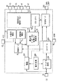
図2は、本発明の回路が履行される8ピンの集積回路(IC)50(IRの部品番号IR2161)の主機能構成要素を示す。一層進歩した履行は、14ピンの集積回路(部品番号IR2162)に見られる。ここではIR2161を詳細に説明し、IR2162に含まれるさらなる機能は他のところで説明する。
First Embodiment FIG. 2 shows the main functional components of an 8-pin integrated circuit (IC) 50 (IR part number IR2161) in which the circuit of the present invention is implemented. More advanced implementations can be found in the 14-pin integrated circuit (part number IR2162). Here, IR 2161 is described in detail, and further functions included in IR 2162 are described elsewhere.
供給電圧(VCC)ピン52、電力及び信号接地(COM)ピン54、電流感知(CS)ピン56、高側ゲート・ドライブ浮動供給(VB)ピン58、高側ゲート・ドライブ出力(HO)ピン60、高側浮動戻り(VS)62、及び低側ゲート・ドライブ出力(LO)ピン64は、International Rectifier Corporationの製品であるIR2156ICまたはIR2157(1)ICの同様に識別されたピンと実質的に同じ機能を行い、かつ実質的に同じ態様で履行され得る。IR2157(1)ICの特徴もまた、米国特許第6,211,623号に記載されており、その開示内容は、その全体においてここに組込まれる。同様に、高側及び低側ドライバ70、下電圧検出回路72、過温度検出回路74、及び欠陥ロジック76は、米国特許第6,211,623号における同様に識別された回路と実質的に同じ機能を行い、かつ実質的に同じ態様で履行され得る。IC50の発振器要素78及び他の要素は、以下の説明から理解され得る。
Supply voltage (VCC)
図3は、出力リード82に接続されたハロゲン・ランプ(図示せず)を、図1における変圧器14と同様に働く変圧器84を介して駆動するように、IR2161 ICとして言及されたInternational Rectifier Corporationの製品として履行されるIC50が接続されている回路80を示す。回路80は、入力リード86を介してAC電力を受け、該回路80中のキャパシタンス90、インダクタンス92、ダイオード94及び96、抵抗98及び100、そしてキャパシタンス102及び104は、図1における従来の回路10における同等の構成要素と同じ機能を行う。回路80は、高側及び低側の電力MOSFET110及び112の動作を介して変圧器84に発振信号を提供する。高側MOSFET110は、そのゲート駆動信号をドライバ70からHOピン60を介して受け、低側MOSFET112は、そのゲート駆動信号をドライバ70からLOピン64を介して受ける。この構成において、出力電圧は、出力変圧器84の負荷変動率に起因する負荷に依存して、またシステム作動周波数に依存して変化する。変圧器84は、一次の漏れインダクタンスを有するので、出力電圧は、周波数が増加するにつれて下降するであろう。
FIG. 3 shows an International Rectifier referred to as an IR 2161 IC to drive a halogen lamp (not shown) connected to the
発振器
図2における発振器要素78を履行するために、図4における発振器回路は、出力信号OOをドライバ70に提供し、この信号は図10に示されている。出力信号は、比較器CMP6の出力からの一連のパルスを含む。OO信号は、デッド・タイム中は高であり、ドライバ70がMOSFET110及び112のいずれか一方にパルスを提供しているときには低である。
Oscillator To implement the
図4を参照すると、比較器CMP6は、制御された電流源により充電されたキャパシタンスC1が閾値電圧Vth1に達すると高出力を提供する。高出力は、また、キャパシタンスC1を所定の電流で放電するために、分路トランジスタMN9をターンオンする。また、高出力は、閾値ロジックが、5Vから0.6Vまで閾値を減少させるMN89をスイッチ・オンすることによってVth1を調整するようにする。比較器出力は、C1上の電圧が0.6V以下に下がってしまうまで、高いままである。このことが起こるまでにかかる時間は、MOSFET110または112のいずれもスイッチ・オンされないデッド・タイムを決定する。C1は、しかしながら、MN8を介して0Vまで即座に放電され得、もしRSET入力にパルスが印加されないならば、比較器出力が直ちに低になるようにして次のサイクルが始まるようにする。このパルスは、以後説明する適応性デッド・タイム回路から送られる。
Referring to FIG. 4, the comparator CMP6 provides a high output when the capacitance C1 charged by the controlled current source reaches the threshold voltage Vth1. The high power also turns on the shunt transistor MN9 to discharge the capacitance C1 with a predetermined current. Also, the high output causes the threshold logic to adjust Vth1 by switching on MN89, which reduces the threshold from 5V to 0.6V. The comparator output remains high until the voltage on C1 has dropped below 0.6V. The time it takes for this to occur determines the dead time during which neither
発振器回路は、入力VCOに与えられる0から+5Vまでの範囲のDC制御電圧から電圧制御される。VCO入力は、図11に示されるシャットダウン回路内の送信ゲートTGATE_SWITCH1を介して外部のCSDピン272に接続される。この送信ゲートは、シャットダウン回路によって検出された欠陥状態中以外は、常時可能化される。ピンCSDからCOM54に接続された外部コンデンサ270は、3つの別々の動作モードを有し、それをこれから詳細に説明するが、概略的には、これらは、(1)ソフト・スタート・タイミングと、(2)電圧補償モードにおける増幅されたCSピン信号の平滑化と、(3)シャットダウン及び自動再スタート・タイミングとである。
The oscillator circuit is voltage controlled from a DC control voltage ranging from 0 to +5 V applied to the input VCO. The VCO input is connected to an
ロジック入力SSN(ソフト・スタートではない)は、VCO入力が0Vにセットされるときに生じる動作の上部周波数を決定する。下部周波数は、SSNの状態とは無関係に同じである。周波数は、VCO電圧が変化するにつれほぼ線形的に変化する。SSNが高であるとき、ソフト・スタート中のVCO電圧の周波数範囲は、それが電圧補償モードで動作しているときの正常作動中のものよりも大きい。IR2161は、電圧をCSピン56に給電する電流感知抵抗を介してMOSFET110、112のハーフ・ブリッジにおける電流を感知することによって、コンバータ出力80における負荷を決定する。
The logic input SSN (not soft start) determines the upper frequency of operation that occurs when the VCO input is set to 0V. The lower frequency is the same regardless of the state of the SSN. The frequency changes approximately linearly as the VCO voltage changes. When SSN is high, the frequency range of the VCO voltage during soft start is greater than that during normal operation when it is operating in voltage compensation mode. IR 2161 determines the load at
ソフト・スタート
ソフト・スタートは、コンバータが最初にスイッチ・オンしたときに生じる。ランプ・フィラメントが冷えているとき、それは熱いときよりも低い抵抗を有し、このことは、図6に示すように高い流入電流をもたらす。このことは、現在用いられている幾つかのシステムにおいては、シャットダウン回路の偽トリガを生成するように見られてきており、安定な連続動作に達する前に、ランプが数回、オン及びオフに点滅することとなる。
Soft start Soft start occurs when the converter is first switched on. When the lamp filament is cold, it has a lower resistance than when it is hot, which results in a high inflow current as shown in FIG. This has been seen in some currently used systems to generate a false trigger of the shutdown circuit, with the lamp turning on and off several times before reaching stable continuous operation. Will blink.
ソフト・スタート回路は、この問題を解消し、同時に、起動時にフィラメントにかかるストレスを減少し、これによりランプの寿命を延ばし得る。図5のソフト・スタート回路は、IC52のVCCピンが下電圧ロックアウト(UVLO)閾値以上に高められたときに動作する。UVLOの作用は、IR2156のようなInternational Rectifier点灯バラスト制御ICと共通である。この点において、発振器は、より高い周波数で開始し、外部のCSD270のコンデンサは、ソフト・スタート中にだけ可能化されたIC内の電流源から充電され始める。ピンCSDにおける電圧が増加するにつれ、周波数は低下し、そうなるにつれ、一層多くの電力がランプに与えられる。CSDにおける電圧が5Vの閾値に達すると、周波数は、30kHz前後の最小値に低下してしまうであろう。IC内のソフト・スタート回路の履行は、図5に見られ得る。ラッチング比較器CMPLTCH1の出力は、周波数範囲を決定する発振器に給電される、ソフト・スタート期間の終わりでの低から高へ行くSSNロジック信号である。ランプ流入電流への影響は、図7に見られ得る。
A soft start circuit can eliminate this problem and at the same time reduce the stress on the filament during start-up, thereby extending the life of the lamp. The soft start circuit of FIG. 5 operates when the VCC pin of
電圧補償モード
ソフト・スタート制御に加えて、発振器周波数は、また、出力電流感知に応答しても制御され得る。CSピンにおける電流は、望まれない高周波数のノイズを除去する低域フィルタを任意選択的に介して、図8の電圧補償回路のCSF入力に与えられる。図8における回路は、正電圧の固定された利得を有する演算増幅器PMOS_OP1を組み込んでいる。出力は、ダイオードQ1及び伝達ゲートTGATE_SWITCH1を介して、外部のCSDコンデンサ及び発振器VCOの入力に与えられる。伝達ゲートは、電圧補償作用が活性化されている時の正常動作モードにある、ソフト・スタート・モード及びシャットダウン・モードにシステムが無いときに、可能化される。電圧補償とは、負荷変動に起因したコンバータの出力電圧における変化を補償するための機構を言っている。ハロゲン変換器は最大電力定格を有するが、高い出力電圧に帰結する幾分軽い負荷で用いられ得る。例えば、2つの並列の50Wランプを駆動する100Wのコンバータが、11.5VのRMS出力電圧を生成し得るが、もし一方のランプが取り除かれるかまたは開回路になった場合には、電圧は12Vに増加し得る。当然、電圧が高ければ高いほど、高いランプ電力を生成し、このことは、ランプ温度を高めてその寿命を減らす。最大負荷においてCSDコンデンサにかかる電圧はおよそ5Vである。PMOS_OP1における電圧は、全波整流された正弦波包絡線内に含まれる発振器周波数におけるパルスから成り、ダイオードQ1は、ピーク整流を提供し、CSDコンデンサは、ピークに比例したDCレベルを生成するよう平滑化を提供する。もし負荷が減少されたならば、CSDコンデンサは、電流源MN1を介して多くのサイクルに渡ってゆっくりと放電される。この回路においては高速応答は不必要である。
In addition to voltage compensated mode soft start control, the oscillator frequency can also be controlled in response to output current sensing. The current at the CS pin is applied to the CSF input of the voltage compensation circuit of FIG. 8 optionally through a low pass filter that removes unwanted high frequency noise. The circuit in FIG. 8 incorporates an operational amplifier PMOS_OP1 with a fixed gain of positive voltage. The output is applied to the input of the external CSD capacitor and the oscillator VCO via the diode Q1 and the transmission gate TGATE_SWITCH1. The transmission gate is enabled when the system is not in soft start mode and shutdown mode, which is in the normal mode of operation when voltage compensation is activated. Voltage compensation refers to a mechanism for compensating for changes in the converter output voltage due to load fluctuations. Halogen converters have a maximum power rating but can be used with somewhat lighter loads resulting in higher output voltages. For example, a 100 W converter driving two parallel 50 W lamps can produce an RMS output voltage of 11.5 V, but if one lamp is removed or becomes an open circuit, the voltage is 12 V Can be increased. Of course, higher voltages produce higher lamp power, which increases the lamp temperature and reduces its lifetime. The voltage across the CSD capacitor at maximum load is approximately 5V. The voltage at PMOS_OP1 consists of pulses at the oscillator frequency contained within the full wave rectified sinusoidal envelope, diode Q1 provides peak rectification, and the CSD capacitor is smoothed to produce a DC level proportional to the peak. Provide If the load is reduced, the CSD capacitor is slowly discharged over many cycles through the current source MN1. In this circuit, a high-speed response is unnecessary.
シャットダウン回路
IR2161におけるシャットダウン回路が図11に示されている。入力CSは、ICの外部のCSピンに接続されている。正常動作中、電流感知抵抗は、最大負荷において
約0.4Vのピーク電流を提供するように選択されている。これは、発振器が必要とされる最小の周波数で作動するようにする、電圧補償モード中にCSDピンにおいて5Vを提供する。もし負荷が最大定格の150%に増加された場合、CSピンにおけるピーク電圧は、結果的に0.5Vに達し、このことは、CMP1の出力が高に行くようにし、INV2を介してMP8をスイッチング・オンする。CSピンにおける信号の高周波成分のために、CMP1は、ライン電圧の半サイクルのピークにおいて高周波パルスを生成する。同様に、過酷な過負荷もしくは出力の短絡が生じたならば、CSにおけるピーク電圧は、INV14の閾値を超え、これにより、その出力は低くなり、MP4をスイッチ・オンさせることとなる。
A shutdown circuit in the shutdown circuit IR2161 is shown in FIG. The input CS is connected to a CS pin outside the IC. During normal operation, the current sensing resistor is selected to provide a peak current of about 0.4V at full load. This provides 5V at the CSD pin during the voltage compensation mode, which allows the oscillator to operate at the minimum frequency required. If the load is increased to 150% of the maximum rating, the peak voltage at the CS pin will eventually reach 0.5V, which will cause the output of CMP1 to go high and turn MP8 through INV2. Switching on. Due to the high frequency component of the signal at the CS pin, CMP1 generates a high frequency pulse at the peak of the half cycle of the line voltage. Similarly, if a severe overload or output short circuit occurs, the peak voltage at CS exceeds the threshold of INV14, which lowers its output and causes MP4 to switch on.
CMP1が高になると、フリップ・フロップRRS1はセットされる。このことは、伝達ゲートTGATE_SWITCH2を可能化してCSDピンをシャットダウン回路に接続し、そしてTGATE_SWITCH1を不可能化してCSDピンを電圧補償回路から遮断する。同時に、MP44がスイッチ・オンされて、CSDコンデンサがMN70を介してほぼ4Vに充電されるようにし、これにより、MN1が保持され、RRS1及びRRS2のR2入力が低く保たれるのを確実にしている。これは、電圧補償及びシャットダウン回路間でのCSDのサイクルごとのスイッチングを避けることである。 When CMP1 goes high, flip-flop RRS1 is set. This enables the transfer gate TGATE_SWITCH2 to connect the CSD pin to the shutdown circuit and disables TGATE_SWITCH1 to disconnect the CSD pin from the voltage compensation circuit. At the same time, MP44 is switched on so that the CSD capacitor is charged to approximately 4V via MN70, thereby ensuring that MN1 is held and the R2 inputs of RRS1 and RRS2 are kept low. Yes. This is to avoid cycle-by-cycle switching of the CSD between voltage compensation and shutdown circuits.
RRS1がセットされている期間中、システムは、図14に示される状態図に示されるように、欠陥タイミング・モードまたは欠陥モードにある。これらのモードにおいて、明確には必要とされない電圧補償回路は不活性となり、周波数は静に留まる。INV14の出力が低いとき、電流は、MP3及びMP4を介して外部のCSDコンデンサ270に供給され、CMP1が高いとき、電流は、MP2及びMP8を介してコンデンサに供給される。外部の電力MOSFET110及び112を短時間内に破壊するであろう非常に高いハーフ(半)・ブリッジ電流をINV14が検出するので、充電速度は、INV14がCMP1よりも一層急速にコンデンサを充電させるように、異なっている。MOSFETが損傷無しで或る時間この電流を維持できるであろうので、CMP1は、コンデンサをゆっくりと充電する。CSD電圧は、VCC(APWRとしてIC内に言及される)に近接した点まで増加するので、PMOSデバイスMP6はスイッチ・オフし、INV4の入力は高から低に行き、MN2によってプル・ダウンされる。INV4の出力は、フリップフロップRRS2をセットしてSDロジック信号を高に行かせる。この信号が高であるとき、システムは、双方のハーフ・ブリッジMOSFETのオフで不可能化され、出力への電力を完全に除去する。結果として、CSピンにおける電流はゼロに降下し、INV14の出力は高に行き、そしてCMP1の出力は低に行くが、RRS1及びRRS2はセットされたままで、システムは欠陥モードに留まる。欠陥モードにおいて、MN3はスイッチ・オンされ、電流シンクMN4を通してCSDを放電し、電圧が徐々に降下するようにする。それがゼロ近くに降下すると、MN1はスイッチ・オフし、RRS2のR2入力はMP6を介して高に引っ張られてSDを低に再度セットし、これにより、発振器が再度作動を開始すること、並びにMOSFETへの出力ドライブが付勢されることを許容する。SDNは同時に高に行き、INV2がAND1を介して高である場合に、フリップフロップRRS1をリセットする。INV2の出力は、CSで検出された過電流欠陥があるときに高である。RRS1がリセットされるとき、TGATE_SWITCH2は不可能化され、TGATE_SWITCH1は可能化され、これにより、CSDを電圧補償回路に接続し、
そしてシャットダウン回路から遮断する。発振器が再スタートし、欠陥が未だ存在するならば、全シーケンスは、欠陥状態がもはや存在しなくなるまで、繰り返される。このことは、図14の状態図に示されている。
During the period when RRS1 is set, the system is in a defect timing mode or a defect mode, as shown in the state diagram shown in FIG. In these modes, voltage compensation circuits that are not explicitly required become inactive and the frequency remains static. When the output of INV14 is low, current is supplied to the
And it shuts off from the shutdown circuit. If the oscillator restarts and the defect still exists, the entire sequence is repeated until the defect state no longer exists. This is illustrated in the state diagram of FIG.
要約すると、過負荷が生じると、次に、システムは、およそ0.5秒の遅延後にシャットダウンする。短絡回路が生じると、システムは、およそ50ミリ秒の遅延後にシャットダウンする。双方の場合において、システムは、およそ0.5秒間、オフに留まり、次に、自動的に再スタートする。過負荷もしくは短絡回路状態が残っているならば、次に、シーケンスは、連続的に反復する。これは、図12及び図13に示されている。この方法で、コンバータは、過熱または要素を損傷することなく、欠陥状態を無制限に許容し得る。 In summary, when an overload occurs, the system then shuts down after a delay of approximately 0.5 seconds. When a short circuit occurs, the system shuts down after a delay of approximately 50 milliseconds. In both cases, the system stays off for approximately 0.5 seconds and then automatically restarts. If an overload or short circuit condition remains, then the sequence repeats continuously. This is illustrated in FIGS. 12 and 13. In this way, the converter can tolerate unlimited fault conditions without overheating or damaging elements.
適応性デッド・タイム
バイポーラ電力トランジスタをベースにした自己発振ハロゲン・コンバータは、システムが常にソフトに切り換わるので、固有に効率的である。DCバスはライン電圧ハーフ・サイクル中に変わるので、デッド・タイムは当然に変わる。同様のレベルの効率を達成するために、デッド・タイムも、本発明においては、同様のソフト・スイッチング(切り換え)を提供するよう順応する。
Self-oscillating halogen converters based on adaptive dead time bipolar power transistors are inherently efficient because the system always switches to soft. Since the DC bus changes during the line voltage half cycle, the dead time naturally changes. In order to achieve a similar level of efficiency, dead time is also adapted in the present invention to provide similar soft switching.
IR2161は、図3のVSピンにおいてMOSFETハーフ・ブリッジ中央点における電圧を感知することにより動作する適応性デッド・タイム機能を含む。高側のMOSFET110がスイッチ・オフされるとき、VSにおける電圧は、変圧器84の漏れインダクタンス及びMOSFET110及び112のドレイン・ソース容量に起因して、0Vにそれる。電圧VSが0Vに達すると、それは、下部のMOSFET112がスイッチ・オンするための正しい時間である。
IR 2161 includes an adaptive dead time function that operates by sensing the voltage at the MOSFET half bridge midpoint at the VS pin of FIG. When the
MOSFET110のゲートを駆動する高側ドライバ出力HOは、図15に示される回路のSPN入力に供給される負に行くパルスによって高にセットされる。それは、RPN入力に供給される負に行くパルスで低にセットされる。SPNパルスは、フリップ・フロップRS1をセットし、D型フリップ・フロップDF1をリセットし、MP30がスイッチ・オフされるようにする。RPNパルスは、DF1のQDN出力が低に行くようにし、HOがVSの高から低への変遷の始まりにおいて低にセットされると同時にMP30をスイッチ・オンする。MP30がスイッチ・オンされると、電流が、VSプラスVCCの電位にあるVBピンからZCに供給される。電流は、HINが低であるのでこの時点で可能化される、図15に示されるMN37及びMN38のミラーに流れる。これは、MN38のドレイン、図10に示される信号Dが低であるようにする。VS電圧がゼロに向かってそれるので、ミラーにおけるさらなる電流が無い点が達成され、MN38のドレインは高に行く。この点において、出力ADTでパルスが発生され、これが図10に示される。ADTパルスはOR4に供給され、MN31を駆動し、図15の高側ドライバ回路のRPN入力得において第2の負に行くパルスを生成する。これはHSRS5には、それがすでにリセットされているので、何の影響も与えないが、DF1がセットされたときにRS1がリセットされたので、DF1をリセットするであろう。このロジックは、MP30をスイッチ・オフし、ZCにはそれ以上の電流は供給されない。その結果、制限された電流だけを供給するような大きさとされているMP30は、VSの高から低へのそらせ(slew)時間中にだけスイッチ・オンされる。
The high side driver output HO that drives the gate of
波形VSが図10に示されており、該図10はまた、図15のためのSPN及びRPN入力を生成する、図16のMN30及びMN31のゲートに供給するパルスをも示している。図10を参照すると、VSの高から低への変遷の始めにおいて、LTRIGでパルスが生じ、そしてVSにおける電圧が0Vに接近してそれる(slew)ときにADTでパルスが生じることが分かり得る。これらパルス間の期間もしくは周期は、デッド・タイムを決定する。これらの信号は、図9の適応性デッド・タイム回路に供給される。RRS1はLTRIGによってセットされ、そして或る理由で、高から低への変遷が検出されない場合には発振器からのADTまたはOONによってリセットされ、システムを固定されたデッド・タイムにデフォルトする。RRS1がセットされると、MP11をスイッチ・オフさせ、MP9及びMP10から成る電流ミラーがコンデンサCBに電流を供給するようにする。結果として、電圧は、VSの検出された高から低へのスルー(slew:そらせ)時間に比例してCB上に存在する。 Waveform VS is shown in FIG. 10, which also shows the pulses supplied to the gates of MN30 and MN31 of FIG. 16 that generate the SPN and RPN inputs for FIG. Referring to FIG. 10, it can be seen that at the beginning of the transition of VS from high to low, a pulse occurs at LTRIG and a pulse occurs at ADT when the voltage at VS slews close to 0V. . The period or period between these pulses determines the dead time. These signals are supplied to the adaptive dead time circuit of FIG. RRS1 is set by LTRIG and for some reason is reset by ADT or OON from the oscillator if no high to low transition is detected, defaulting the system to a fixed dead time. When RRS1 is set, MP11 is switched off and a current mirror consisting of MP9 and MP10 supplies current to capacitor CB. As a result, voltage is present on CB in proportion to the detected high to low slew time of VS.
同じ方法で、高から低へのスルー(slew:そらせ)時間を感知することが可能ではないので、類似であると仮定され得る高から低へのスルー(そらせ)時間を再生することにより正しいデッド・タイムを決定する。MOSFET112へのゲート・ドライブLOが低に行くとき、図9に示されるフリップ・フロップRRS2をセットするHTRIGパルスが生じる。この点において、MP13及びMP14から成るもう1つの同一の電流源が可能化されて、CBが充電を始める。CA上の電圧がCB上の電圧を超えると、比較器CMP3の出力は高に行き、これにより、スルー(そらせ)時間は複製される。CMP3の出力が高に行くと、フリップ・フロップRRS2はリセットされ、従って、正しいデッド・タイム・パルスが、RRS2のQ出力において低から高への変遷の間生成される。フリップ・フロップRRS1及びRRS2からの出力は、NORゲートNOR7に供給されてADTO出力を生成する。ADTO出力は、いずれかのデッド・タイム中に低であり、出力MOSFET110または112のいずれかがスイッチ・オンされたときに高である信号から成る。ADTO信号は、各デッド・タイムの終りでRSET出力にパルスを生成し、該パルスは、図4の発振器に戻して供給され、C1を放電し、次のサイクルを始める。この方法で、図10に示される発振器出力OOは、適応性デッド・タイム回路に追従し、反転されることができ、そして次に、図17に示される出力ロジック回路に信号OONを介して供給される。信号OONは、ANDゲートAND2及びAND3を介してLO及びHOのブランキングを提供する。
Since it is not possible to sense the slew time from high to low in the same way, the correct dead by reproducing the high to low slew time that can be assumed to be similar.・ Determine time. When the gate drive LO to MOSFET 112 goes low, an HTRIG pulse is generated that sets flip-flop RRS2 shown in FIG. At this point, another identical current source consisting of MP13 and MP14 is enabled and the CB begins charging. When the voltage on CA exceeds the voltage on CB, the output of comparator CMP3 goes high, thereby replicating the slew time. When the output of CMP3 goes high, flip-flop RRS2 is reset, so the correct dead time pulse is generated during the low-to-high transition at RRS2's Q output. Outputs from the flip-flops RRS1 and RRS2 are supplied to a NOR gate NOR7 to generate an ADTO output. The ADTO output consists of a signal that is low during either dead time and is high when either
位相カット調光操作
ハロゲン・コンバータは、主に平滑化されないDCバス電圧のために、トライアックまたはトランジスタをベースにした位相カット調光システムを介して操作される。IR2161の場合において、調光器におけるトライアックまたはトランジスタがオフの期間中、DCバス電圧はゼロに降下するということが考慮されてきた。このことは、電流が引き上げられ続けるので、VCCにおける電圧がUVLOの負に行く閾値以下に降下することに帰結し得る。位相カット調光操作中にソフト・スタート回路がハーフ・サイクルごとに再トリガされる可能性を避けるために、第2の負に行く閾値が下電圧ロックアウト回路に追加されてきており、これにより、VCCは、ソフト・スタート回路がリセットされるようになるためにはこのより低い閾値以下に降下しなければならない。この第2の閾値は、第1のもの以下のほぼ2Vである。VCCが第1の閾値以下に降下すると、ICは、マイクロ・パワー・モードに行き、VCCコンデンサからの非常に小さい電流だけを引き上げる。従って、VCCにおけるこのコンデンサがさらに2Vだけ放電するために一つのライン電圧ハーフ・サイクルよりも長くかかり、結果としてソフト・スタート回路はリセットされない。
Phase Cut Dimming Operation Halogen converters are operated via a TRIAC or transistor based phase cut dimming system, mainly for unsmoothed DC bus voltage. In the case of IR2161, it has been considered that the DC bus voltage drops to zero during the TRIAC or transistor off period of the dimmer. This can result in the voltage at VCC dropping below the UVLO negative threshold as the current continues to be pulled up. To avoid the possibility of the soft start circuit being retriggered every half cycle during phase cut dimming operation, a second negative threshold has been added to the undervoltage lockout circuit, thereby VCC must fall below this lower threshold for the soft start circuit to be reset. This second threshold is approximately 2V below the first. When VCC falls below the first threshold, the IC goes into micro power mode and pulls only a very small current from the VCC capacitor. Therefore, it takes longer than one line voltage half cycle to discharge this capacitor at VCC by an additional 2V, resulting in the soft start circuit not being reset.
追加の機能
IR2161は、IR2157(1)のようなInternational Rectifierによって製造された他のICにおいても履行される追加の機能(例えば、過温度のシャットダウン)を有する。
Additional functions IR 2161 have additional functions (eg, over temperature shutdown) that are also implemented in other ICs manufactured by International Rectifier such as IR 2157 (1).
第2の実施形態
図18は、本発明の回路が実施される集積回路(IC)50の第2の実施形態の主な機能構成要素を示す。供給電圧(VCC)ピン52、電力及び信号接地(COM)ピン54、電流感知(CS)ピン56、高側ゲート・ドライブ浮動供給(VB)ピン58、高側ゲート・ドライバ出力(HO)ピン60、高側浮動戻り(VS)62、及び低側ゲート・ドライバ出力(LO)ピン64は、International Rectifier Corporationの製品であるIR2156IC及びIR2157ICの同様に識別されたピンと実質的に同じ作用を行い、そして実質的に同じ態様で履行され得る。IR2157ICの特徴も、米国特許第6,211,623号に記載されており、その開示内容は、その全体においてここに組込まれる。同様に、高側及び低側ドライバ70、下電圧検出回路72、過温度検出回路74、及び欠陥ロジック76は、米国特許第6,211,623号において同様に識別された回路と実質的に同じ作用を行い、そして実質的に同じ態様で履行され得る。発振器要素78及びIC50の他の構成要素は、以下の説明から理解され得る。
Second Embodiment FIG. 18 shows the main functional components of a second embodiment of an integrated circuit (IC) 50 in which the circuit of the present invention is implemented. Supply voltage (VCC)
図19は、IR2162ICとして言及されるInternational Rectifier Corporationの製品として履行されるIC50が、ハロゲン・ランプ(図示せず)を駆動するように接続されている回路80を示す。ハロゲン・ランプは、図1における変圧器14と同様に作用する変圧器84を介して出力リード82に接続される。回路80は、入力リード86を介してAC電力を受け、この場合、キャパシタンス90、インダクタンス92、ダイオード94及び96、抵抗98及び100、並びにキャパシタンス102及び104は、図1の従来の回路10における同等の構成要素と同じ作用を行う。回路80は、高及び低側電力MOSFRT110及び112の動作により発振信号を変圧器84に与える。高側MOSFET110は、そのゲート・ドライブ信号をHOピン60を介してドライバ70から受け、低側MOSFET112は、そのゲート・ドライブ信号をLOピン64を介してドライバ70から受ける。
FIG. 19 shows a
図18における発振器要素78を履行するために、図20における発振器回路120は、ドライバ70に出力信号OSCを与える。出力波形122は、出力信号が比較器124の出力からの一連のパルスを含むということを示す。OSC信号はデッド・タイム中は高であり、ドライバ70がMOSFET110及び112のいずれか一つにパルスを提供しているときは低である。
To implement the
比較器124は、制御された電流源132により充電されたキャパシタンス130が閾値電圧Vthに達したときに高出力を提供する。高出力は、また、キャパシタンス130を放電するために分路トランジスタ134をターン・オンする。高出力は、また、閾値ロジック136にVthを調節させて、比較器124が低に行き、次に、適切な時刻に再度高に行くのを確実にする。
The
制御された電流源132は、フィードバック電圧による制御及びソフト・スタート中の制御を含む幾つかの方法で制御される。電流源132がキャパシタンス130を充電する速度を変えれば、次に、発振周波数を変える。電流源132による充電速度は、従って、同等の周波数範囲を有する。
The controlled
フィードバック電圧制御のために、電流源132がキャパシタンス130を充電する速度は、比較器142からの出力によって制御される。例えば、電流源132は、40kHzのような出力波形122の最小周波数を確実にする最小電流レベルを有し得る。しかし、充電ポンプ入力(VFB)ピン144におけるフィードバック電圧がバンドギャップ基準電圧Vrefを超えると、比較器142は、誤差増幅器補償(COMP)ピン148を介して外部のキャパシタンス146を充電し、電流源132への電圧が高まるようにしてキャパシタンス130の充電速度が増加するようにし、これにより、出力波形122の周波数を増加する。増加速度は、キャパシタンス146の大きさによって決定される。
For feedback voltage control, the rate at which
図19に示されるように、VFBピン144は、出力リード82を介してハロゲン・ランプに与えられる信号を示すように接続されたノード150からの電圧を受けるように接続される。変圧器84は、追加の二次コイル154を有し、該コイルの一方のリードは、ダイオード156、抵抗158及び160、並びに抵抗160を横切って接続されたキャパシタンス162を介して接地に接続される。コイル154がダイオード156の導通方向に信号を受け始めると、抵抗158を通る電流は、最初にキャパシタンス162を充電し、ノード150における電圧を高め、そして抵抗160を通して電流を生成する。信号がダイオード156の非導通方向に変わると、抵抗158を通る電流は停止し、キャパシタンス162は抵抗160を通して放電し、ノード150における電圧が降下するのを許容する。結果として、VFBピン144における電圧は、出力信号の各サイクルの部分中にVrefを超える。
As shown in FIG. 19,
このようにして、キャパシタンス146の大きさは、出力信号の周波数を決定する:もしキャパシタンス146が大きければ、電流源132は、ほぼ最小周波数に対する速度でキャパシタンス130を充電するが、より小さいキャパシタンス146が選択された場合には、電流源132は、より早い速度でキャパシタンス130を充電し、より高い出力信号周波数を生成する。
In this way, the magnitude of the
同様に、出力信号周波数は、ソフト・スタート回路180から電流源142への信号によって、より高い周波数から最小の周波数まで下方に掃引され得る。図21に示されるフリップ・フロップ182は、トランジスタ184が起動時に最初にターン・オンされるように、適切な回路(図示せず)により起動前にリセットされ、外部のキャパシタンス190を調光ランプ(CDIM)ピン192を介して充電するように、電流が抵抗186及び188を介して流れるのを許容する。ノード194における電圧は最初は低いので、トランジスタ196も最初はターン・オンされ、それにより、トランジスタ184を流れる電流は分割される。幾らかの電流は、抵抗198を介して電流源132に流れ、それ故、コンデンサ130に流れ、急速充電及び一層高い出力信号周波数を許容する。
Similarly, the output signal frequency can be swept down from a higher frequency to a minimum frequency by a signal from
ノード194における電圧は、キャパシタンス190の充電に起因して上昇するので、トランジスタ196はターン・オフされ、コンデンサ130は、一層ゆっくりと充電し、出力信号をその最小周波数まで下方に持っていく。次に、CDIMピン192上の電圧は、それが閾値電圧Vthを超えるまで上昇する。この時点で、比較器200は、高い信号を提供し、フリップ・フロップ182をセットし、従って、トランジスタ184をターン・オフし、これによりソフト・スタート回路180は完全に切り換えられ、次回にフリップ・フロップ182が起動時にリセットされるまで、出力信号周波数にさらなるどんな影響をも与えない。
As the voltage at
図22及び図23は、起動時におけるランプ電流へのソフト・スタート回路180の影響を示す。図22は、ソフト・スタート回路180が無い場合のランプ電流を示し、図23は、ソフト・スタート回路180が有る場合のランプ電流を示す。図22において、ランプ電流は、一層高い初期値でスタートし、安定状態に降下する。他方、図23においては、ランプ電流は、安定状態よりも僅かに高いだけの一層低い初期値でスタートし、一層徐々に降下し、このように、スイッチ・オン時にランプのフィラメントにかかるストレスを減少する。図23における一層低い初期値は、一層高い出力信号周波数が電流の流れを減少するので、生じる。
22 and 23 show the influence of the
電圧フィードバック及びソフト・スタート制御に加えて、制御された電流源132は、また、出力電流感知に応答しても制御され得る。そして、OSC信号の周波数は、キャパシタンス130を横切って接続されたリセット・トランジスタ210によって成就される、デッド・タイム調整を介しても制御され得る。
In addition to voltage feedback and soft start control, the controlled
図24は、発振器回路120の部分である適応性デッド・タイム(ADT)回路220を示し、該回路は、高から低への遷移じのデッド・タイムを検出し、その結果を用いてパルス化されたリセット(RST)信号を提供して、低から高への遷移の間のデッド・タイムを修正し、冷えた作動電力MOSFETを許容する。図25は、回路220の動作を示す幾つかの波形を示す。
FIG. 24 shows an adaptive dead time (ADT)
ADT回路220は、発振器回路120から出力(OSC)信号を受け、また、交流OSCパルスの立ち上がりエッジを示す低及び高のトリガ・パルスを受ける。低及び高のトリガ・パルスは、適切な回路(図示せず)によってOSC信号から導出される。OSC信号はトランジスタ222のゲートに与えられ、低及び高のトリガ信号は、それぞれフリップ・フロップ(RS1)224及びフリップ・フロップ(RS2)226をセットするように接続される。
The
OSC信号は、ドライブ信号間にデッド・タイムを与えるように高に行くが、ドライブ信号を提供し始めるためには低に行く。デッド・タイムの開始を示す、OSC信号におけるパルスの立ち上がりエッジは、トランジスタ222をターン・オンする。回路220は、OSC信号におけるパルスの立ち上がりエッジだけが、VSの高から低への変遷中に、すなわちOSC信号における1つおきのパルス中に、トランジスタ222をターン・オンするようにロジック(図示せず)を含む。図25で左に示す、高から低への変遷中、VSピン62上の電圧は、VBUS電圧からCOM電圧への変遷を行い、電流はトランジスタ228に流れ、従って、トランジスタ230もまたターン・オンし、そしてADT信号を低に保持する。VS電圧がCOM電圧へのすべての道をそれる(slew)とき、トランジスタ230はスイッチ・オフし、ADT信号は、抵抗234を介して接続される供給電圧に応答して高に行く。
The OSC signal goes high to give a dead time between the drive signals, but goes low to begin providing the drive signal. The rising edge of the pulse in the OSC signal indicating the start of dead time turns on
高のADT信号は、低のトリガ・パルスにより高から低への変遷の開始時にセットされていたフリップ・フロップ224をリセットする。低のトリガは、HOがデッド・タイムの開始時にスイッチ・オフするとき、高に行く。結果として、ADT OUT信号は、高から低へのデッド・タイム中にだけ高である。フリップ・フロップ224がリセットされると、そのQ出力は、低のADT OUT信号を提供し始め、そしてNORゲート232は、図20におけるトランジスタ210をリセットするよう高のRST信号を提供することにより応答し、OSCパルスが低に行くように発振器60をリセットし、デッド・タイムを終結し、そして新しい発振器サイクル/タイミング・ランプ(傾斜)を始める。
A high ADT signal resets the flip-
フリップ・フロップ224が、このデッド・タイムの開始時に低のトリガ・パルスによってセットされるとき、そのQN出力は、スイッチ回路236のENN_B入力に低の信号を提供し、該回路236は、そのOUT_Bリードを介してキャパシタンス(CB)240に充電電流を提供することにより応答する。
When flip-
スイッチング回路236は、そのIN入力に適切な電流源(図示せず)から電流を受け、以下のように動作する。そのENN_A及びENN_B入力が双方とも高であるとき、スイッチ回路236は、そのIN入力をそのCOM出力に接続する。ENN_Aが低であるとき、スイッチ回路236は、そのIN入力をそのOUT_A出力に接続する。ENN_Bが低であるとき、スイッチ回路236はそのIN入力をそのOUT_B出力に接続する。ADT回路220は、フリップ・フロップ224及び226の少なくとも一方が常にリセットされるので、ENN_A及びENN_Bが決して同時には低にはならないのを確実にする。
The
ADT信号が高に行くとき、ENN_Bもまた高に行き、それ故、スイッチ回路236は、キャパシタンス240を充電するのを停止する。図25に示すように、キャパシタンス(CB)240を横切る電圧は上昇を停止して、ほぼ一定を保持し、このようにして、図25の左のOSCパルス中のデッド・タイムの期間に関する情報を格納する。
When the ADT signal goes high, ENN_B also goes high, so
図25の右に示される、引き続く低から高へのOSCパルスの立ち上がりエッジは、VSピン62上の電圧における低から高への変遷中のデッド・タイムの始まりを示す。VS電圧が上昇するにつれ、トランジスタ222及び228を通る電流の流れは、トランジスタ230をターン・オンし、ADT信号が低に行くのを許容する。しかし、同時にキャパシタンス242を通して受信される高のトリガ信号パルスはフリップ・フロップ226をセットし、それ故、そのQ出力は高のCOMP Out信号を提供する。NORゲート232は、応答して低のRST信号を提供し始める。
The rising edge of the subsequent low-to-high OSC pulse, shown to the right of FIG. 25, indicates the beginning of dead time during the low-to-high transition in the voltage on
フリップ・フロップ226がセットされると、そのQN出力は、スイッチ回路236のENN_A入力に低の信号を提供し、スイッチ回路236がキャパシタンス(CA)244に充電電流を提供するようにする。キャパシタンスCA244及びCB240は、それぞれ比較器246の非反転及び反転入力に接続される。従って、キャパシタンス244上の電圧がキャパシタンス240上の電圧を超えると、比較器246は、その出力に高のCOMP信号を提供し始め、フリップ・フロップ226をリセットし、それ故、COMP Outは低に行く。低のCOMP Out信号は、NORゲート232に高のRST信号を提供させてトランジスタ210をリセットさせる。結果として、OSCパルスは低に行き、それ故、デッド・タイムを終結させて、新しい発振器サイクル/タイミング・ランプ(傾斜)を始める。
When flip-
フリップ・フロップ226が高のCOMP信号によりリセットされると、そのQN出力は高に行く。従って、スイッチ回路236は、ENN_A及びENN_Bの双方に高の入力を有し、コンデンサ240及び244のいずれも充電されている。高のQN出力は、キャパシタンス254を介してトランジスタ250及び252のゲートにパルスを提供して、キャパシタンス240及び244の双方を0Vに放電する。結果として、低から高へのVS変遷中のデッド・タイムの期間は、直ぐ前の高から低への変遷デッド・タイム中にキャパシタンス240に蓄えられた電荷によってのみ決定される。上述したように、蓄えられた電荷は、高から低への変遷デッド・タイムの期間を示し、それ故、デッド・タイム期間は、IC50への外部の構成要素を用いることなく、ADT回路220によって調整される。
When flip-
図26は、図18におけるタイミング要素254及びピーク・レベル検出要素252を含むシャットダウン回路250を示す。過負荷または短絡回路状態が検出されると、シャットダウン回路250は、不能化信号を提供する。該不能化信号は、高のとき、欠陥ロジック76に、高及び低の出力信号HO及びLOを不能化させる。過負荷または短絡回路状態が終了すると、シャットダウン回路250は自動リセットを行う。
FIG. 26 shows a
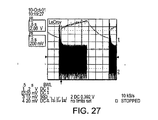
電流感知CSピン56上の電圧は電流感知抵抗260を介して受信され、高周波スパイクを除去するためにキャパシタンス262によってフィルタリングされる。フィルタリングされた結果は、比較器264及び266の“+”入力に与えられる。比較器264は、その“+”入力を1.2Vと比較することにより短絡回路状態を検出し、他方、比較器266は、その“+”入力を0.6Vと比較することにより過負荷状態を検出する。いずれの比較器からの高出力も、シャットダウン・タイミング・コンデンサ(CSD)ピン272を介して、図19に示される外部のキャパシタンス270を充電させる。しかし、比較器264は、例証的に50キロオームの抵抗274を介してキャパシタンス270を充電し、他方、比較器266は、例証的に500キロオームの抵抗276を介して充電する。抵抗274及び276における違いの結果として、比較器264は、比較器266が充電するよりも急速にキャパシタンス270を充電する。換言すれば、短絡回路状態の検出は、短い遅延を有し、過負荷状態の検出は、長い遅延を有する。
The voltage on current
比較器264及び266の一方がキャパシタンス270を1V以上に充電するまで、比較器280を高出力を提供し、フリップ・フロップ282はそのリセット状態を保持する。1V以上で、比較器280は低出力を提供し、フリップ・フロップ282がセットされるのを許容する。キャパシタンス270が5Vを通過したとき、比較器284は、フリップ・フロップ282をセットする高出力を提供し、そしてHO及びLO出力を不能化する高い不能化出力を提供する。高い不能化出力は、また、トランジスタ290をターン・オンし、これにより、キャパシタンス270が、例証的に1メガオームである抵抗292を介して放電するのを許容するが、比較器264及び266の一方が高出力を提供している間は、キャパシタンス270が放電するのを阻止する。キャパシタンス270が再度1V以下に降下すると、比較器280は再度高出力を提供し、フリップ・フロップ282をリセットし、それ故、不能化出力は低に行き、HO及びLO出力はもはや不能化されない。
Until one of
図27及び図28は、図27に示される過負荷状態と、図28に示される短絡回路状態と、に応答したシャットダウン回路250の動作を比較している。各図は、電流感知抵抗260を横切る電圧の波形(明るい灰色)を、CSDピン272における電圧によって測定されるキャパシタンス270を横切る電圧の波形(暗い灰色)と比較している。図から分かるように、過負荷状態に対するシャットダウンは比較的ゆっくりしており、短絡回路状態に対するシャットダウンは比較的早い。しかし、再スタート前の遅延は、いずれの場合においても同じ固定時間である。
27 and 28 compare the operation of the
図19に示されるように、調光制御入力(VDIM)ピン300は、マイクロコントローラ(図示せず)によってまたはICに対する外部の他のソースによって与えられるDC制御電圧であって良い調光制御信号を受ける。サンプルACライン電圧(SYNC)ピン302は、回路80によって入力ピン86において受信されたACライン電圧から導出された信号を受ける。これらの信号に応答して、図18に示される位相カット調光要素304は、立下りエッジの自己調光を行う。
As shown in FIG. 19, a dimming control input (VDIM)
例証的にキャパシタンス90及びインダクタンス92によって行われるフィルタリングの後、ピン86からのACライン電圧は、ダイオード94及び96によって整流され、COMピン54上の電圧を参照して感知される。図29は、例証的に各々220キロオームであって良い抵抗310及び312を介して与えられる結果のAC半波信号を示す。2つの半波信号はノード314で合計されて、SYNCピン302への信号を提供する。
Illustratively after filtering performed by
SYNCピン302からの合計された半波信号は、図30に波形342によって示されるように、調光ランプ(ramp:傾斜)回路340によって受信される。回路340は、ACライン電圧に同期化されたランプ(ramp)波形を提供する、図18における位相カット調光要素304の部分である。このランプ波形は、比較器(図示せず)の一方のリードに与えられ、VDIMピン300からの調光制御信号は、他方に与えられて、以下で一層充分に説明される可能化信号として働くことができるチョップ化された高周波出力を生成する。このサンプル及び効率的な調光技術は、フィラメント・ランプに対して理想的である。
The summed half-wave signal from the
SYNCピン302からの半波信号は、例証的に5キロオームである抵抗344を横切る電圧を制御する。この電圧は、半波信号が一半サイクルの終了時に降下するときトランジスタ346をターン・オフし、半波信号が次の半サイクルの始めに上昇するとき、オンに戻す。トランジスタ346がターン・オフされるとき、ノード348における電圧は上昇し、トランジスタ346がターン・オンされるとき再度降下し、このようにして、波形352によって示されるように、トランジスタ350のゲートにパルス化された信号を与える。
The half wave signal from
トランジスタ350がオフである比較的長い期間中、電流源360は、調光ランプ(CDIM)ピン192を介して外部のキャパシタンス190を充電する。キャパシタンス190は、また、ソフト・スタート回路180によっても使用されるので、電流源360は、図21−23に関して上述したソフト・スタートの完了後だけに可能化され得る。充電中、ノード362における電圧は、波形364に示されるように、上方に傾斜する。しかし、トランジスタ350が波形352におけるパルスによってターン・オンされると、キャパシタンス190は、トランジスタ350を介して放電し、波形364における降下エッジを生成する。波形352におけるパルスの後、充電が再度始まる。
During a relatively long period when
ノード362は、比較器(図示せず)の“+”リードに接続され得、VDIMピン300は、“−”リードに接続され得る。結果として、比較器は、ライン周波数に同期化した矩形波形を提供する。例えば、矩形波形は、ランプ(傾斜)波形が調光制御信号を超えるまで低に留まり、次に、ランプ波形における次の降下エッジまで高に行くことができ、従って、そのデューティ・サイクルは、VDIMピン300への調光制御信号に依存する。比較器出力は適切なゲート(図示せず)に与えられて、ドライバ70からのHO及びLO出力を不能化及び可能化し得る。この履行において、ドライバ70によって制御されるハーフ・ブリッジは、各主サイクルの初期の部分の間だけスイッチングし、その後、スイッチングを停止し、従って、VSピン62における電圧は、初期の部分の間だけ駆動され、その後、減衰路をたどる。
図31における波形は、位相カット調光要素304の動作を示しており、下部の波形は、CDIMピン192におけるランプ波形電圧を示しており、上部の波形は、VSピン62におけるチョップ化された高周波出力電圧を示している。VDIMピン300に与えられる調光制御信号を調節することにより、矩形波形のデューティ・サイクルは変化され、その最大値の0%と100%との間でVSピン62における平均出力電圧を調整する。一方、ライン電圧ゼロ交差は、DCバス上の電圧に影響せず、該電圧は、もはや負荷が無いという理由で位相カット調光によって出力が不能化されたときにライン電圧がどんな電圧にあったとしてもその電圧に留まる。結果として、SYNC信号は、ブリッジ整流器の前に検出されなければならない。
The waveform in FIG. 31 shows the operation of the phase cut dimming
図18の回路50におけるバンドギャップ基準380は、Vref、比較器142のための基準電圧、並びに種々の他の基準電圧を提供することができる。回路50における5V調整器382は、調整された5V出力(5VOUT)ピン384を介してマイクロコントローラのための5V調整された出力電圧を提供する。
The
IC50の、より単純で、より低価格の、8ピンの同等物も、上述のこれら特徴を有して製造されてきたが、より簡単な調整機構を有している。
The simpler, less expensive, 8-pin equivalent of
上述した新しいICは、ハロゲン・ランプを駆動するための商業的に入手可能な最初のICで有ると期待され、それらICの応用は、他のフィラメント・ランプに拡張し得るものである。これら新規なICの履行は、大いに信頼性を得ることができ、現存の回路よりも多くの機能を有することができ、潜在的に低価格で製造することができる。良好な実験結果が得られた。 The new ICs described above are expected to be the first commercially available ICs for driving halogen lamps, and their IC applications can be extended to other filament lamps. The implementation of these new ICs can be highly reliable, can have more functions than existing circuits, and can be manufactured at potentially lower cost. Good experimental results were obtained.
50・・・集積回路(IC)、70・・・高側及び低側ドライバ、72・・・下電圧検出回路、74・・・過温度検出回路、76・・・欠陥ロジック、78・・・IC50の発振器要素(適応性デッド・タイム回路)、180・・・ソフト・スタート回路、254・・・シャットダウン回路。
50: Integrated circuit (IC), 70: High side and low side drivers, 72: Under voltage detection circuit, 74: Over temperature detection circuit, 76: Defect logic, 78 ... IC50 oscillator element (adaptive dead time circuit), 180... Soft start circuit, 254.
Claims (6)
前記制御信号を発生するための発振器と、
起動時に前記ランプに過度の電流を避けるように前記発振器を制御するソフト・スタート回路と、
を備えた駆動回路。 A drive circuit for providing a control signal to a power semiconductor device that supplies power to a filament lamp,
An oscillator for generating the control signal;
A soft start circuit that controls the oscillator to avoid excessive current in the lamp during start-up;
Drive circuit.
前記制御信号を発生するための発振器と、
負荷における変動を補償するように前記発振器を制御する電圧補償回路と、
を備えた駆動回路。 A drive circuit for providing a control signal to a power semiconductor device that supplies power to a filament lamp,
An oscillator for generating the control signal;
A voltage compensation circuit that controls the oscillator to compensate for variations in the load;
Drive circuit.
前記制御信号を発生するための発振器と、
欠陥状態に応答して前記発振器をシャットダウンしそして自動的に再スタートさせるためのシャットダウン回路と、
を備えた駆動回路。 A drive circuit for providing a control signal to a power semiconductor device that supplies power to a filament lamp,
An oscillator for generating the control signal;
A shutdown circuit for shutting down and automatically restarting the oscillator in response to a fault condition;
Drive circuit.
前記制御信号を発生するための発振器と、
前記電力半導体デバイスの冷却作動を提供するように前記発振器を制御する適応性デッド・タイム回路と、
を備えた駆動回路。 A drive circuit for providing a control signal to a power semiconductor device that supplies power to a filament lamp,
An oscillator for generating the control signal;
An adaptive dead time circuit that controls the oscillator to provide cooling operation of the power semiconductor device;
Drive circuit.
前記制御信号を発生するための発振器と、
前記ランプを調光するように前記発振器を制御する調光回路と、
を備えた駆動回路。 A drive circuit for providing a control signal to a power semiconductor device that supplies power to a filament lamp,
An oscillator for generating the control signal;
A dimming circuit for controlling the oscillator to dimm the lamp;
Drive circuit.
前記制御信号を発生するための発振器と、
該発振器のための制御回路と、
を備え、集積回路内で実施される駆動回路。
A drive circuit for providing a control signal to a power semiconductor device that supplies power to a filament lamp,
An oscillator for generating the control signal;
A control circuit for the oscillator;
And a drive circuit implemented in an integrated circuit.
Applications Claiming Priority (3)
| Application Number | Priority Date | Filing Date | Title |
|---|---|---|---|
| US34323601P | 2001-12-31 | 2001-12-31 | |
| US39829802P | 2002-07-22 | 2002-07-22 | |
| PCT/US2002/041836 WO2003059017A1 (en) | 2001-12-31 | 2002-12-30 | Basic halogen convertor ic |
Related Child Applications (1)
| Application Number | Title | Priority Date | Filing Date |
|---|---|---|---|
| JP2007198049A Division JP2007280973A (en) | 2001-12-31 | 2007-07-30 | Control circuit serving its role in integrated circuit in order to provide control signal to power semiconductor device for supplying output power to filament lamp |
Publications (2)
| Publication Number | Publication Date |
|---|---|
| JP2005514756A true JP2005514756A (en) | 2005-05-19 |
| JP2005514756A5 JP2005514756A5 (en) | 2006-01-19 |
Family
ID=26993387
Family Applications (2)
| Application Number | Title | Priority Date | Filing Date |
|---|---|---|---|
| JP2003559198A Pending JP2005514756A (en) | 2001-12-31 | 2002-12-30 | Basic halogen converter IC |
| JP2007198049A Withdrawn JP2007280973A (en) | 2001-12-31 | 2007-07-30 | Control circuit serving its role in integrated circuit in order to provide control signal to power semiconductor device for supplying output power to filament lamp |
Family Applications After (1)
| Application Number | Title | Priority Date | Filing Date |
|---|---|---|---|
| JP2007198049A Withdrawn JP2007280973A (en) | 2001-12-31 | 2007-07-30 | Control circuit serving its role in integrated circuit in order to provide control signal to power semiconductor device for supplying output power to filament lamp |
Country Status (7)
| Country | Link |
|---|---|
| US (2) | US7321201B2 (en) |
| JP (2) | JP2005514756A (en) |
| CN (1) | CN1618256A (en) |
| AU (1) | AU2002360849A1 (en) |
| DE (1) | DE10297588T5 (en) |
| TW (1) | TW200304339A (en) |
| WO (1) | WO2003059017A1 (en) |
Cited By (2)
| Publication number | Priority date | Publication date | Assignee | Title |
|---|---|---|---|---|
| JP2007305394A (en) * | 2006-05-11 | 2007-11-22 | Toshiba Lighting & Technology Corp | Dimmer device |
| JP2013122879A (en) * | 2011-12-12 | 2013-06-20 | Mitsubishi Electric Corp | Lighting control device |
Families Citing this family (27)
| Publication number | Priority date | Publication date | Assignee | Title |
|---|---|---|---|---|
| EP1793484B1 (en) * | 2005-12-02 | 2010-02-24 | STMicroelectronics S.r.l. | A method and device for driving power converters |
| CN2636576Y (en) * | 2003-06-19 | 2004-08-25 | 悦诚贸易(国际)有限公司 | Cold light sheet driving device |
| US7924584B1 (en) | 2004-01-29 | 2011-04-12 | Marvell International Ltd. | Power supply switching circuit for a halogen lamp |
| US7436160B2 (en) * | 2004-02-19 | 2008-10-14 | International Rectifier Corporation | Half bridge adaptive dead time circuit and method |
| US7265503B2 (en) * | 2004-04-08 | 2007-09-04 | International Rectifier Corporation | Applications of halogen convertor control IC |
| US7525293B1 (en) * | 2004-12-06 | 2009-04-28 | Marvell International Ltd. | Power supply switching circuit for a halogen lamp |
| DE102006016983B4 (en) * | 2006-04-06 | 2014-03-20 | E.G.O. Elektro-Gerätebau GmbH | Switching power supply with overload and short-circuit protection |
| GB0617393D0 (en) * | 2006-09-04 | 2006-10-11 | Lutron Electronics Co | Variable load circuits for use with lighting control devices |
| US7541751B2 (en) * | 2007-03-05 | 2009-06-02 | Mdl Corporation | Soft start control circuit for lighting |
| US7696701B2 (en) * | 2007-04-05 | 2010-04-13 | Osram Sylvania Inc. | Power supply for halogen lamp having an inverter and output circuit |
| KR101386975B1 (en) * | 2007-07-03 | 2014-04-21 | 페어차일드코리아반도체 주식회사 | Lamp ballast circuit and driving method thereof |
| US7888925B2 (en) * | 2007-07-23 | 2011-02-15 | Intersil Americas Inc. | Load current compensation in synchronous power converters |
| US7906948B2 (en) * | 2007-07-23 | 2011-03-15 | Intersil Americas Inc. | Threshold voltage monitoring and control in synchronous power converters |
| TW200913445A (en) * | 2007-07-23 | 2009-03-16 | Intersil Inc | Dead-time transition adjustments for synchronous power converters |
| KR101473805B1 (en) * | 2007-10-30 | 2014-12-24 | 삼성디스플레이 주식회사 | Backlight driver and liquid crystal display comprising the same |
| US8749209B2 (en) | 2008-05-05 | 2014-06-10 | Infineon Technologies Austria Ag | System and method for providing adaptive dead times |
| US8076860B2 (en) * | 2008-11-06 | 2011-12-13 | Osram Sylvania Inc. | Power converter and power conversion method with reduced power consumption |
| US7982413B2 (en) * | 2009-05-01 | 2011-07-19 | Grenergy Opto, Inc. | Electronic ballast with dimming control from power line sensing |
| US8378695B2 (en) | 2009-06-17 | 2013-02-19 | Infineon Technologies Austria Ag | Determining the dead time in driving a half-bridge |
| TWI420964B (en) * | 2009-08-24 | 2013-12-21 | Green Solution Tech Co Ltd | Driving circuit and controller for controlling the same |
| US8339056B1 (en) * | 2010-06-17 | 2012-12-25 | Universal Lighting Technologies, Inc. | Lamp ballast with protection circuit for input arcing and line interruption |
| KR20130052359A (en) * | 2011-11-11 | 2013-05-22 | 삼성전기주식회사 | Control ic having auto recovery circuit, auto recovery circuit of control ic, power converter system and method for auto-recovery in control ic |
| CN102723886B (en) * | 2012-06-26 | 2015-02-18 | 上海新进半导体制造有限公司 | High power factor switch power supply and controller and control method thereof |
| TWI505644B (en) * | 2012-08-08 | 2015-10-21 | Leadtrend Tech Corp | Circuit with adjustable phase delay and a feedback voltage and method for adjusting phase delay and a feedback voltage |
| US9306446B2 (en) * | 2012-12-07 | 2016-04-05 | Atmel Corporation | Fault protection and correction of line and load faults |
| WO2014188229A1 (en) * | 2013-05-20 | 2014-11-27 | Xmart Chip Micro-Electronics Co., Ltd. | Electronic ballast control |
| CN106059278B (en) * | 2016-05-31 | 2018-08-21 | 中国电子科技集团公司第三十八研究所 | A kind of frequency SS (soft start) control circuit |
Family Cites Families (21)
| Publication number | Priority date | Publication date | Assignee | Title |
|---|---|---|---|---|
| BE786136A (en) | 1971-07-13 | 1973-01-11 | Philips Nv | DEVICE FOR FEEDING AT LEAST ONE GAS AND / OR VAPOR DISCHARGE LAMP |
| GB2244608A (en) | 1990-04-23 | 1991-12-04 | P I Electronics Pte Ltd | High frequency drive circuit for a fluorescent lamp |
| JPH0494097A (en) | 1990-08-10 | 1992-03-26 | Hitachi Lighting Ltd | Inverter for halogen lamp |
| JPH0574581A (en) | 1991-09-13 | 1993-03-26 | Matsushita Electric Works Ltd | Incandescent lamp lighting device |
| JPH0574580A (en) | 1991-09-13 | 1993-03-26 | Matsushita Electric Works Ltd | High-frequency lighting device for incandescent lamp |
| JPH0632588A (en) | 1991-10-24 | 1994-02-08 | Kobe Steel Ltd | Operating condition display device for construction machine |
| JP3459142B2 (en) | 1995-08-09 | 2003-10-20 | ソニー株式会社 | Drive pulse output limiting circuit |
| US6002213A (en) * | 1995-10-05 | 1999-12-14 | International Rectifier Corporation | MOS gate driver circuit with analog input and variable dead time band |
| US5796215A (en) * | 1996-01-29 | 1998-08-18 | International Rectifier Corporation | Soft start circuit for self-oscillating drivers |
| JPH10223381A (en) | 1997-01-31 | 1998-08-21 | Toshiba Lighting & Technol Corp | Power supply unit, lighting device and lighting system |
| US6008593A (en) * | 1997-02-12 | 1999-12-28 | International Rectifier Corporation | Closed-loop/dimming ballast controller integrated circuits |
| JPH1131593A (en) | 1997-07-10 | 1999-02-02 | Toshiba Lighting & Technol Corp | Lamp-lighting device, and lighting system |
| CN1175468C (en) | 1997-09-03 | 2004-11-10 | 皇家菲利浦电子有限公司 | Incandescent lamp |
| US5925990A (en) * | 1997-12-19 | 1999-07-20 | Energy Savings, Inc. | Microprocessor controlled electronic ballast |
| US6211623B1 (en) * | 1998-01-05 | 2001-04-03 | International Rectifier Corporation | Fully integrated ballast IC |
| WO2000035252A2 (en) | 1998-12-07 | 2000-06-15 | Systel Development And Industries Ltd. | Digital lamp ballast |
| CN1784108A (en) * | 2000-06-19 | 2006-06-07 | 国际整流器有限公司 | Ballast control IC with minimal internal and external components |
| ATE348354T1 (en) * | 2000-10-20 | 2007-01-15 | Int Rectifier Corp | BALLAST CONTROL IC WITH POWER FACTOR CORRECTION |
| US6900599B2 (en) * | 2001-03-22 | 2005-05-31 | International Rectifier Corporation | Electronic dimming ballast for cold cathode fluorescent lamp |
| US6856519B2 (en) * | 2002-05-06 | 2005-02-15 | O2Micro International Limited | Inverter controller |
| US7109665B2 (en) * | 2002-06-05 | 2006-09-19 | International Rectifier Corporation | Three-way dimming CFL ballast |
-
2002
- 2002-12-30 AU AU2002360849A patent/AU2002360849A1/en not_active Abandoned
- 2002-12-30 CN CN02827685.XA patent/CN1618256A/en active Pending
- 2002-12-30 TW TW091137888A patent/TW200304339A/en unknown
- 2002-12-30 DE DE10297588T patent/DE10297588T5/en not_active Withdrawn
- 2002-12-30 JP JP2003559198A patent/JP2005514756A/en active Pending
- 2002-12-30 WO PCT/US2002/041836 patent/WO2003059017A1/en active Application Filing
-
2003
- 2003-05-21 US US10/443,525 patent/US7321201B2/en not_active Expired - Fee Related
-
2006
- 2006-11-15 US US11/560,216 patent/US7558081B2/en not_active Expired - Fee Related
-
2007
- 2007-07-30 JP JP2007198049A patent/JP2007280973A/en not_active Withdrawn
Cited By (2)
| Publication number | Priority date | Publication date | Assignee | Title |
|---|---|---|---|---|
| JP2007305394A (en) * | 2006-05-11 | 2007-11-22 | Toshiba Lighting & Technology Corp | Dimmer device |
| JP2013122879A (en) * | 2011-12-12 | 2013-06-20 | Mitsubishi Electric Corp | Lighting control device |
Also Published As
| Publication number | Publication date |
|---|---|
| CN1618256A (en) | 2005-05-18 |
| AU2002360849A1 (en) | 2003-07-24 |
| US7558081B2 (en) | 2009-07-07 |
| TW200304339A (en) | 2003-09-16 |
| DE10297588T5 (en) | 2004-11-18 |
| US7321201B2 (en) | 2008-01-22 |
| US20070069658A1 (en) | 2007-03-29 |
| JP2007280973A (en) | 2007-10-25 |
| WO2003059017A1 (en) | 2003-07-17 |
| US20040012346A1 (en) | 2004-01-22 |
Similar Documents
| Publication | Publication Date | Title |
|---|---|---|
| US7558081B2 (en) | Basic halogen convertor IC | |
| US6151232A (en) | Power supply circuit utilizing a piezoelectric transformer that supplies power to a load whose impedance varies depending on temperature | |
| US6008593A (en) | Closed-loop/dimming ballast controller integrated circuits | |
| US9532415B2 (en) | Multi-mode dimmer interfacing including attach state control | |
| US6175195B1 (en) | Triac dimmable compact fluorescent lamp with dimming interface | |
| JP3958368B2 (en) | stabilizer | |
| US6011357A (en) | Triac dimmable compact fluorescent lamp with low power factor | |
| US6043611A (en) | Dimmable compact fluorescent lamp | |
| US6020689A (en) | Anti-flicker scheme for a fluorescent lamp ballast driver | |
| US7408307B2 (en) | Ballast dimming control IC | |
| US6949888B2 (en) | Dimming ballast control IC with flash suppression circuit | |
| US7436127B2 (en) | Ballast control circuit | |
| JP2007311360A (en) | Stabilizer control ic with power factor correction circuit | |
| JPH0329299A (en) | Lamp controller | |
| JPH0773983A (en) | Electronic method ballast of zero voltage switching method for fluorescent lamp | |
| US8212591B2 (en) | Control of a resonant switching system with monitoring of the working current in an observation window | |
| JP4700289B2 (en) | Load power consumption adjustment method, load power consumption adjustment circuit, and electric lighting device for lamp | |
| US5982110A (en) | Compact fluorescent lamp with overcurrent protection | |
| JP4122206B2 (en) | Integrated circuit for closed loop / dimming stability control | |
| MX2010011978A (en) | Voltage fed programmed start ballast. |
Legal Events
| Date | Code | Title | Description |
|---|---|---|---|
| A521 | Request for written amendment filed |
Free format text: JAPANESE INTERMEDIATE CODE: A523 Effective date: 20051121 |
|
| A131 | Notification of reasons for refusal |
Free format text: JAPANESE INTERMEDIATE CODE: A131 Effective date: 20070130 |
|
| A601 | Written request for extension of time |
Free format text: JAPANESE INTERMEDIATE CODE: A601 Effective date: 20070501 |
|
| A602 | Written permission of extension of time |
Free format text: JAPANESE INTERMEDIATE CODE: A602 Effective date: 20070510 |
|
| A521 | Request for written amendment filed |
Free format text: JAPANESE INTERMEDIATE CODE: A523 Effective date: 20070730 |
|
| A131 | Notification of reasons for refusal |
Free format text: JAPANESE INTERMEDIATE CODE: A131 Effective date: 20080318 |
|
| A601 | Written request for extension of time |
Free format text: JAPANESE INTERMEDIATE CODE: A601 Effective date: 20080520 |
|
| A602 | Written permission of extension of time |
Free format text: JAPANESE INTERMEDIATE CODE: A602 Effective date: 20080527 |
|
| A601 | Written request for extension of time |
Free format text: JAPANESE INTERMEDIATE CODE: A601 Effective date: 20080818 |
|
| A602 | Written permission of extension of time |
Free format text: JAPANESE INTERMEDIATE CODE: A602 Effective date: 20080825 |
|
| A521 | Request for written amendment filed |
Free format text: JAPANESE INTERMEDIATE CODE: A523 Effective date: 20080918 |
|
| A02 | Decision of refusal |
Free format text: JAPANESE INTERMEDIATE CODE: A02 Effective date: 20090331 |