JP2005509266A - Protective layer for forming molecular electronic devices - Google Patents
Protective layer for forming molecular electronic devices Download PDFInfo
- Publication number
- JP2005509266A JP2005509266A JP2002575993A JP2002575993A JP2005509266A JP 2005509266 A JP2005509266 A JP 2005509266A JP 2002575993 A JP2002575993 A JP 2002575993A JP 2002575993 A JP2002575993 A JP 2002575993A JP 2005509266 A JP2005509266 A JP 2005509266A
- Authority
- JP
- Japan
- Prior art keywords
- layer
- molecular
- electronic device
- region
- protective layer
- Prior art date
- Legal status (The legal status is an assumption and is not a legal conclusion. Google has not performed a legal analysis and makes no representation as to the accuracy of the status listed.)
- Pending
Links
- 238000005442 molecular electronic Methods 0.000 title claims abstract description 59
- 239000011241 protective layer Substances 0.000 title claims abstract description 55
- 239000010410 layer Substances 0.000 claims abstract description 100
- 239000002052 molecular layer Substances 0.000 claims abstract description 34
- 238000000034 method Methods 0.000 claims abstract description 33
- 230000015654 memory Effects 0.000 claims abstract description 22
- 238000000059 patterning Methods 0.000 claims abstract description 5
- 239000004020 conductor Substances 0.000 claims description 26
- 239000012212 insulator Substances 0.000 claims description 23
- 229910052751 metal Inorganic materials 0.000 claims description 14
- 239000002184 metal Substances 0.000 claims description 14
- 238000002955 isolation Methods 0.000 claims description 5
- 230000003647 oxidation Effects 0.000 claims description 5
- 238000007254 oxidation reaction Methods 0.000 claims description 5
- 229910044991 metal oxide Inorganic materials 0.000 claims description 3
- 150000004706 metal oxides Chemical class 0.000 claims description 3
- 238000000926 separation method Methods 0.000 claims description 3
- 230000002542 deteriorative effect Effects 0.000 claims 1
- 230000008569 process Effects 0.000 abstract description 15
- 230000000593 degrading effect Effects 0.000 abstract description 3
- 238000004519 manufacturing process Methods 0.000 abstract 1
- 239000000758 substrate Substances 0.000 description 9
- 239000004065 semiconductor Substances 0.000 description 8
- 230000006870 function Effects 0.000 description 7
- 238000000427 thin-film deposition Methods 0.000 description 7
- 239000000463 material Substances 0.000 description 6
- 229910052782 aluminium Inorganic materials 0.000 description 5
- XAGFODPZIPBFFR-UHFFFAOYSA-N aluminium Chemical compound [Al] XAGFODPZIPBFFR-UHFFFAOYSA-N 0.000 description 5
- 239000002070 nanowire Substances 0.000 description 5
- 239000002904 solvent Substances 0.000 description 5
- RTAQQCXQSZGOHL-UHFFFAOYSA-N Titanium Chemical compound [Ti] RTAQQCXQSZGOHL-UHFFFAOYSA-N 0.000 description 4
- 230000008859 change Effects 0.000 description 4
- 239000010936 titanium Substances 0.000 description 4
- 229910052719 titanium Inorganic materials 0.000 description 4
- 239000010408 film Substances 0.000 description 3
- 230000001681 protective effect Effects 0.000 description 3
- VYPSYNLAJGMNEJ-UHFFFAOYSA-N Silicium dioxide Chemical compound O=[Si]=O VYPSYNLAJGMNEJ-UHFFFAOYSA-N 0.000 description 2
- WYURNTSHIVDZCO-UHFFFAOYSA-N Tetrahydrofuran Chemical compound C1CCOC1 WYURNTSHIVDZCO-UHFFFAOYSA-N 0.000 description 2
- 239000011149 active material Substances 0.000 description 2
- 230000015572 biosynthetic process Effects 0.000 description 2
- 238000005229 chemical vapour deposition Methods 0.000 description 2
- 239000002131 composite material Substances 0.000 description 2
- 238000000313 electron-beam-induced deposition Methods 0.000 description 2
- 238000005530 etching Methods 0.000 description 2
- 238000001459 lithography Methods 0.000 description 2
- 238000001755 magnetron sputter deposition Methods 0.000 description 2
- 229920003229 poly(methyl methacrylate) Polymers 0.000 description 2
- 239000000126 substance Substances 0.000 description 2
- 230000005641 tunneling Effects 0.000 description 2
- 229910004298 SiO 2 Inorganic materials 0.000 description 1
- XUIMIQQOPSSXEZ-UHFFFAOYSA-N Silicon Chemical compound [Si] XUIMIQQOPSSXEZ-UHFFFAOYSA-N 0.000 description 1
- 230000004888 barrier function Effects 0.000 description 1
- 150000001875 compounds Chemical class 0.000 description 1
- 238000000151 deposition Methods 0.000 description 1
- 238000010586 diagram Methods 0.000 description 1
- 238000009792 diffusion process Methods 0.000 description 1
- 238000004090 dissolution Methods 0.000 description 1
- 238000005401 electroluminescence Methods 0.000 description 1
- 238000000609 electron-beam lithography Methods 0.000 description 1
- 230000008571 general function Effects 0.000 description 1
- 239000013547 langmuir monolayer Substances 0.000 description 1
- 230000007246 mechanism Effects 0.000 description 1
- 230000009149 molecular binding Effects 0.000 description 1
- 230000001590 oxidative effect Effects 0.000 description 1
- TWNQGVIAIRXVLR-UHFFFAOYSA-N oxo(oxoalumanyloxy)alumane Chemical compound O=[Al]O[Al]=O TWNQGVIAIRXVLR-UHFFFAOYSA-N 0.000 description 1
- 230000035515 penetration Effects 0.000 description 1
- 238000000206 photolithography Methods 0.000 description 1
- 229920002120 photoresistant polymer Polymers 0.000 description 1
- 238000001020 plasma etching Methods 0.000 description 1
- 229920000642 polymer Polymers 0.000 description 1
- 239000004926 polymethyl methacrylate Substances 0.000 description 1
- 230000009467 reduction Effects 0.000 description 1
- 229910052594 sapphire Inorganic materials 0.000 description 1
- 239000010980 sapphire Substances 0.000 description 1
- 229910052710 silicon Inorganic materials 0.000 description 1
- 239000010703 silicon Substances 0.000 description 1
- 235000012239 silicon dioxide Nutrition 0.000 description 1
- 239000000377 silicon dioxide Substances 0.000 description 1
- 239000002356 single layer Substances 0.000 description 1
- YLQBMQCUIZJEEH-UHFFFAOYSA-N tetrahydrofuran Natural products C=1C=COC=1 YLQBMQCUIZJEEH-UHFFFAOYSA-N 0.000 description 1
- 238000001075 voltammogram Methods 0.000 description 1
Images


Classifications
-
- H—ELECTRICITY
- H01—ELECTRIC ELEMENTS
- H01L—SEMICONDUCTOR DEVICES NOT COVERED BY CLASS H10
- H01L29/00—Semiconductor devices adapted for rectifying, amplifying, oscillating or switching, or capacitors or resistors with at least one potential-jump barrier or surface barrier, e.g. PN junction depletion layer or carrier concentration layer; Details of semiconductor bodies or of electrodes thereof ; Multistep manufacturing processes therefor
- H01L29/66—Types of semiconductor device ; Multistep manufacturing processes therefor
- H01L29/68—Types of semiconductor device ; Multistep manufacturing processes therefor controllable by only the electric current supplied, or only the electric potential applied, to an electrode which does not carry the current to be rectified, amplified or switched
- H01L29/76—Unipolar devices, e.g. field effect transistors
- H01L29/772—Field effect transistors
- H01L29/78—Field effect transistors with field effect produced by an insulated gate
-
- G—PHYSICS
- G11—INFORMATION STORAGE
- G11C—STATIC STORES
- G11C13/00—Digital stores characterised by the use of storage elements not covered by groups G11C11/00, G11C23/00, or G11C25/00
- G11C13/0002—Digital stores characterised by the use of storage elements not covered by groups G11C11/00, G11C23/00, or G11C25/00 using resistive RAM [RRAM] elements
- G11C13/0009—RRAM elements whose operation depends upon chemical change
- G11C13/0014—RRAM elements whose operation depends upon chemical change comprising cells based on organic memory material
-
- B—PERFORMING OPERATIONS; TRANSPORTING
- B82—NANOTECHNOLOGY
- B82Y—SPECIFIC USES OR APPLICATIONS OF NANOSTRUCTURES; MEASUREMENT OR ANALYSIS OF NANOSTRUCTURES; MANUFACTURE OR TREATMENT OF NANOSTRUCTURES
- B82Y10/00—Nanotechnology for information processing, storage or transmission, e.g. quantum computing or single electron logic
-
- G—PHYSICS
- G11—INFORMATION STORAGE
- G11C—STATIC STORES
- G11C13/00—Digital stores characterised by the use of storage elements not covered by groups G11C11/00, G11C23/00, or G11C25/00
- G11C13/02—Digital stores characterised by the use of storage elements not covered by groups G11C11/00, G11C23/00, or G11C25/00 using elements whose operation depends upon chemical change
-
- H—ELECTRICITY
- H01—ELECTRIC ELEMENTS
- H01L—SEMICONDUCTOR DEVICES NOT COVERED BY CLASS H10
- H01L21/00—Processes or apparatus adapted for the manufacture or treatment of semiconductor or solid state devices or of parts thereof
- H01L21/70—Manufacture or treatment of devices consisting of a plurality of solid state components formed in or on a common substrate or of parts thereof; Manufacture of integrated circuit devices or of parts thereof
- H01L21/71—Manufacture of specific parts of devices defined in group H01L21/70
- H01L21/768—Applying interconnections to be used for carrying current between separate components within a device comprising conductors and dielectrics
- H01L21/76801—Applying interconnections to be used for carrying current between separate components within a device comprising conductors and dielectrics characterised by the formation and the after-treatment of the dielectrics, e.g. smoothing
- H01L21/76829—Applying interconnections to be used for carrying current between separate components within a device comprising conductors and dielectrics characterised by the formation and the after-treatment of the dielectrics, e.g. smoothing characterised by the formation of thin functional dielectric layers, e.g. dielectric etch-stop, barrier, capping or liner layers
- H01L21/76834—Applying interconnections to be used for carrying current between separate components within a device comprising conductors and dielectrics characterised by the formation and the after-treatment of the dielectrics, e.g. smoothing characterised by the formation of thin functional dielectric layers, e.g. dielectric etch-stop, barrier, capping or liner layers formation of thin insulating films on the sidewalls or on top of conductors
-
- H—ELECTRICITY
- H01—ELECTRIC ELEMENTS
- H01L—SEMICONDUCTOR DEVICES NOT COVERED BY CLASS H10
- H01L21/00—Processes or apparatus adapted for the manufacture or treatment of semiconductor or solid state devices or of parts thereof
- H01L21/70—Manufacture or treatment of devices consisting of a plurality of solid state components formed in or on a common substrate or of parts thereof; Manufacture of integrated circuit devices or of parts thereof
- H01L21/71—Manufacture of specific parts of devices defined in group H01L21/70
- H01L21/768—Applying interconnections to be used for carrying current between separate components within a device comprising conductors and dielectrics
- H01L21/76838—Applying interconnections to be used for carrying current between separate components within a device comprising conductors and dielectrics characterised by the formation and the after-treatment of the conductors
- H01L21/76886—Modifying permanently or temporarily the pattern or the conductivity of conductive members, e.g. formation of alloys, reduction of contact resistances
- H01L21/76888—By rendering at least a portion of the conductor non conductive, e.g. oxidation
-
- G—PHYSICS
- G11—INFORMATION STORAGE
- G11C—STATIC STORES
- G11C2213/00—Indexing scheme relating to G11C13/00 for features not covered by this group
- G11C2213/70—Resistive array aspects
- G11C2213/77—Array wherein the memory element being directly connected to the bit lines and word lines without any access device being used
-
- H—ELECTRICITY
- H01—ELECTRIC ELEMENTS
- H01L—SEMICONDUCTOR DEVICES NOT COVERED BY CLASS H10
- H01L21/00—Processes or apparatus adapted for the manufacture or treatment of semiconductor or solid state devices or of parts thereof
- H01L21/70—Manufacture or treatment of devices consisting of a plurality of solid state components formed in or on a common substrate or of parts thereof; Manufacture of integrated circuit devices or of parts thereof
- H01L21/71—Manufacture of specific parts of devices defined in group H01L21/70
- H01L21/768—Applying interconnections to be used for carrying current between separate components within a device comprising conductors and dielectrics
- H01L21/76801—Applying interconnections to be used for carrying current between separate components within a device comprising conductors and dielectrics characterised by the formation and the after-treatment of the dielectrics, e.g. smoothing
- H01L21/76822—Modification of the material of dielectric layers, e.g. grading, after-treatment to improve the stability of the layers, to increase their density etc.
- H01L21/76823—Modification of the material of dielectric layers, e.g. grading, after-treatment to improve the stability of the layers, to increase their density etc. transforming an insulating layer into a conductive layer
-
- H—ELECTRICITY
- H10—SEMICONDUCTOR DEVICES; ELECTRIC SOLID-STATE DEVICES NOT OTHERWISE PROVIDED FOR
- H10K—ORGANIC ELECTRIC SOLID-STATE DEVICES
- H10K10/00—Organic devices specially adapted for rectifying, amplifying, oscillating or switching; Organic capacitors or resistors having a potential-jump barrier or a surface barrier
- H10K10/701—Organic molecular electronic devices
-
- H—ELECTRICITY
- H10—SEMICONDUCTOR DEVICES; ELECTRIC SOLID-STATE DEVICES NOT OTHERWISE PROVIDED FOR
- H10K—ORGANIC ELECTRIC SOLID-STATE DEVICES
- H10K19/00—Integrated devices, or assemblies of multiple devices, comprising at least one organic element specially adapted for rectifying, amplifying, oscillating or switching, covered by group H10K10/00
Landscapes
- Engineering & Computer Science (AREA)
- Physics & Mathematics (AREA)
- Power Engineering (AREA)
- Microelectronics & Electronic Packaging (AREA)
- Condensed Matter Physics & Semiconductors (AREA)
- General Physics & Mathematics (AREA)
- Computer Hardware Design (AREA)
- Nanotechnology (AREA)
- Chemical & Material Sciences (AREA)
- Manufacturing & Machinery (AREA)
- Mathematical Physics (AREA)
- Theoretical Computer Science (AREA)
- Crystallography & Structural Chemistry (AREA)
- Ceramic Engineering (AREA)
- Semiconductor Memories (AREA)
- Design And Manufacture Of Integrated Circuits (AREA)
- Semiconductor Integrated Circuits (AREA)
- Internal Circuitry In Semiconductor Integrated Circuit Devices (AREA)
- Formation Of Insulating Films (AREA)
Abstract
【課題】 処理中に電子デバイスのアクティブ分子層の元の状態を保持する分子電子デバイスを形成するプロセスが記載される。
【解決手段】 一態様では、下側ワイヤ層と上側ワイヤ層との間に配置される分子層を有する分子電子デバイスを形成する方法を提供する。本発明の方法によれば、保護層が配設され、それにより上側ワイヤ層のパターニング中に分子層が劣化するのを防ぐ。この製造プロセスから形成される分子電子デバイス構造およびメモリシステムが記載される。A process for forming a molecular electronic device that retains the original state of an active molecular layer of the electronic device during processing is described.
In one aspect, a method of forming a molecular electronic device having a molecular layer disposed between a lower wire layer and an upper wire layer is provided. According to the method of the present invention, a protective layer is provided, thereby preventing the molecular layer from degrading during the patterning of the upper wire layer. A molecular electronic device structure and memory system formed from this manufacturing process is described.
Description
本発明は、分子電子デバイスを形成するためのシステムおよび方法に関する。 The present invention relates to systems and methods for forming molecular electronic devices.
種々の異なる分子電子論理回路およびメモリデバイスが提案されている。 A variety of different molecular electronic logic circuits and memory devices have been proposed.
たとえば、1つの分子電子デバイス構造では、分子層(たとえば、ラングミュア−ブロジェット膜)が一対の導電層(たとえば、一対の金属層、金属層およびドープ半導体層、あるいは一対のドープ半導体層)間に挟まれる。分子層は薄い絶縁性の膜としての役割を果たし、その膜は、トンネル接合デバイスあるいはスイッチングデバイスとして構成される場合がある金属−絶縁体−金属(MIM)構造において、あるいは論理デバイスもしくはエレクトロルミネセンスデバイスとして構成される場合がある金属−絶縁体−半導体(MIS)構造において用いることができる。 For example, in one molecular electronic device structure, a molecular layer (eg, Langmuir-Blodgett film) is between a pair of conductive layers (eg, a pair of metal layers, a metal layer and a doped semiconductor layer, or a pair of doped semiconductor layers). Sandwiched. The molecular layer serves as a thin insulating film that can be configured as a tunnel junction device or a switching device in a metal-insulator-metal (MIM) structure, or as a logic device or electroluminescence. It can be used in metal-insulator-semiconductor (MIS) structures that may be configured as devices.
米国特許第6,128,214号は、ナノスケールデバイスの2次元のアレイから形成される分子ワイヤ・クロスバー・メモリ(MWCM)システムとして構成される別の分子電子デバイス構造を記載する。各MWCMデバイスは、一対の交差するワイヤの交点(すなわち接合部)に形成され、その場所において、少なくとも1つの分子結合種が一対の交差するワイヤ間で双安定分子スイッチとしての役割を果たす。結果として形成されるデバイス構造は、抵抗、ダイオードあるいは非対称非線形の抵抗として構成されることができる。各MWCMデバイスの状態は、比較的高いが、破壊するほど高くはない状態変化用の電圧を印加することにより変更することができ、状態変化を引き起こさない電圧で読み取られることができる。さらに他の分子電子デバイスも提案されている。
本発明は、処理中に電子デバイスのアクティブ分子層の元の状態を保持する分子電子デバイスを形成する新規のプロセスを提供することを目的とする。さらに、本発明は新規の分子電子デバイス構造、およびこの形成プロセスで形成される新規のメモリシステムを提供することを目的とする。 The present invention seeks to provide a novel process for forming a molecular electronic device that retains the original state of the active molecular layer of the electronic device during processing. It is a further object of the present invention to provide a novel molecular electronic device structure and a novel memory system formed by this formation process.
一態様では、本発明は、下側ワイヤ層と上側ワイヤ層との間に配置される分子層を有する分子電子デバイスを形成する方法を提供する。本発明の方法によれば、保護層が設けられ、それにより分子層が上側ワイヤ層のパターニング中に劣化するのを防ぐ。本発明の実施形態は、以下の機構のうちの1つあるいは複数の機構を含むことができる。 In one aspect, the present invention provides a method of forming a molecular electronic device having a molecular layer disposed between a lower wire layer and an upper wire layer. According to the method of the present invention, a protective layer is provided, thereby preventing the molecular layer from degrading during the patterning of the upper wire layer. Embodiments of the invention can include one or more of the following mechanisms.
保護層の選択された領域は、エッチングにより除去されることが好ましい。保護層の選択された領域は、電気導体から絶縁体に変換できるか、または絶縁体から電気導体に変換できることが好ましい。 The selected region of the protective layer is preferably removed by etching. The selected region of the protective layer can preferably be converted from an electrical conductor to an insulator or from an insulator to an electrical conductor.
一実施形態では、分子電子デバイスを包囲する分離保護領域が電気導体から絶縁体に変換される。たとえば、保護層には金属層を用いることができ、分離保護領域は酸化によって絶縁体に変換されることができる。 In one embodiment, the isolated protective region surrounding the molecular electronic device is converted from an electrical conductor to an insulator. For example, a metal layer can be used for the protective layer, and the isolation protective region can be converted into an insulator by oxidation.
別の実施形態では、上側ワイヤ層と下側ワイヤ層との間に配置されるデバイス保護領域が絶縁体から電気導体に変換される。たとえば、保護層はアンチヒューズ構造を有することができ、デバイス保護領域は、デバイス保護領域に電圧を印加することにより電気導体に変換されることができる。 In another embodiment, a device protection region disposed between the upper and lower wire layers is converted from an insulator to an electrical conductor. For example, the protective layer can have an antifuse structure and the device protection region can be converted to an electrical conductor by applying a voltage to the device protection region.
一実施形態では、選択された保護領域が上側ワイヤ層を画定するように変換される。この実施形態では、変換されない保護領域は上側ワイヤ層に対応する。 In one embodiment, the selected protected area is converted to define an upper wire layer. In this embodiment, the unconverted protected area corresponds to the upper wire layer.
いくつかの実施形態では、パターニングされた上側ワイヤ層が保護層上に配置される。上側ワイヤ層は、保護層上にリフトオフ層を配置し、リフトオフ層上に導電層を配置し、リフトオフ層を溶解することによりパターニングされることができる。 In some embodiments, a patterned upper wire layer is disposed on the protective layer. The upper wire layer can be patterned by disposing a lift-off layer on the protective layer, disposing a conductive layer on the lift-off layer, and dissolving the lift-off layer.
別の態様では、本発明は、下側ワイヤ層と、デバイス領域において下側ワイヤ層上に配置される分子層と、保護層とを含む分子電子デバイスを提供する。保護層は分子層上に配置され、電気導体領域と絶縁体領域とを有する。 In another aspect, the present invention provides a molecular electronic device that includes a lower wire layer, a molecular layer disposed on the lower wire layer in a device region, and a protective layer. The protective layer is disposed on the molecular layer and has an electric conductor region and an insulator region.
別の態様では、本発明は、上述の分子電子デバイスに相当するデバイスのアレイを含む分子メモリシステムを提供する。 In another aspect, the present invention provides a molecular memory system comprising an array of devices corresponding to the molecular electronic devices described above.
本発明の他の特徴および利点は、図面および特許請求の範囲を含む、以下に記載される説明から明らかになるであろう。 Other features and advantages of the invention will become apparent from the following description, including the drawings and the claims.
以下に記載される詳細な説明では、類似のデバイスを特定するために類似の参照番号が用いられる。さらに、図面は例示的な実施形態の主な機構を概略的に例示することを意図している。その図面は、実際の実施形態の全ての機構を示すことや、図示されるデバイスの相対的な寸法を示すことを意図するわけではなく、縮尺どおりにも描かれていない。 In the detailed description set forth below, like reference numerals are used to identify like devices. Furthermore, the drawings are intended to schematically illustrate the main features of the exemplary embodiments. The drawings are not intended to illustrate all features of an actual embodiment, nor to illustrate the relative dimensions of the illustrated device, and are not drawn to scale.
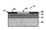
図1を参照すると、一実施形態では、分子電子デバイス10は、0°より大きな角度で交差する2つの導電性ワイヤ12、14を含む。各ワイヤ12、14は、金属あるいはドープ半導体材料から形成されることができる。双安定分子あるいは分子化合物16の層(記号Rによって示される)が、ワイヤ12、14の間に挟まれる。ワイヤ12、14の交差部分に配置される特定の1つあるいは複数の分子18(記号Rsによって示される)は、スイッチ分子として機能し、分子電子デバイス10のアクティブな部分に対応する。
Referring to FIG. 1, in one embodiment, molecular
動作時に、分子電子デバイス10の状態は、比較的高い状態変化用の電圧をワイヤ12、14に印加することにより変更することができる。状態変化用の電圧の大きさは、スイッチ分子18を酸化あるいは還元するのに十分な大きさである。スイッチ分子18は、電荷のバランスをとり、分子種の一方が酸化(あるいは還元)される際に、他方の分子種が還元(あるいは酸化)されるように協動する一対のレドックス分子種を含むことができる。
In operation, the state of the molecular
動作時に、一例では、一方の分子種が還元され、関連する分子種(レドックス対の他方)が酸化されることができる。別の例では、一方の分子種が還元され、ワイヤ12、14のうちの一方が酸化されることができる。第3の例では、一方の分子種が酸化され、ワイヤ12、14のうちの一方が還元されることができる。第4の例では、一方のワイヤが酸化され、他方のワイヤに関連する酸化物が還元されることができる。
In operation, in one example, one molecular species can be reduced and the associated molecular species (the other of the redox couple) can be oxidized. In another example, one molecular species can be reduced and one of the
これらの各例では、酸化あるいは還元が、2つのワイヤ間のトンネル効果距離あるいはトンネル効果障壁高に影響を及ぼし、それにより、ワイヤ接合部を越える電荷輸送の速度を指数関数的に変更する。この電子的な機能は、分子電子デバイス10を電気的スイッチとして動作させるための基礎としての役割を果たす。分子電子デバイス10の全般的な機能に関するさらに細かい点は、米国特許第6,128,214号から得ることができる。
In each of these examples, oxidation or reduction affects the tunneling distance or tunneling barrier height between two wires, thereby exponentially changing the rate of charge transport across the wire junction. This electronic function serves as a basis for operating the molecular
上記のように分子電子デバイス10は、アクティブ分子層18を元の状態に保持するように形成されることができる。図2〜図8Bを参照すると、一実施形態では、分子電子デバイス10は以下のように形成することができる。
As described above, the molecular
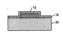
最初に図2、図3Aおよび図3Bを参照する。パターニングされた下側ワイヤ層12は、基板20上に配置することができる(ステップ22)。基板20は、絶縁性の金属、たとえば、半導体基板から形成される酸化物層(たとえば、シリコン基板上に形成される二酸化シリコン(SiO2)層)あるいはサファイアから形成されることができる。
Reference is first made to FIGS. 2, 3A and 3B. The patterned
下側ワイヤ層12は、導電性の金属あるいはドープ半導体材料から形成されることができる。たとえば、一実施形態では、下側ワイヤ層12は、上側にアルミニウム酸化物をコーティングされた(〜1ないし2nm厚)アルミニウム層(〜0.01ないし0.1μm厚)から形成される。下側層12は、物理的薄膜堆積プロセス(たとえば、マグネトロンスパッタリングまたは電子ビーム堆積)あるいは化学的薄膜堆積プロセス(たとえば、化学気相成長)を含む、従来の薄膜堆積プロセスによって基板20上に堆積されることができる。パターニング後(たとえば、リソグラフィによる)、下側ワイヤ層12は、約1nm〜数μmの範囲の幅寸法を有することができる。
The
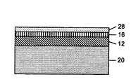
図4Aおよび図4Bを参照すると、分子層16が下側ワイヤ層12上に配置される(図2のステップ26)。分子層16は、種々の異なる双安定分子種から形成されることができる。たとえば、1999年3月29日に出願の米国特許出願第09/282,048号に記載されるロタクサン分子のうちの1つあるいは複数の分子がある。いくつかの実施形態では、選択された分子種が、溶媒(たとえば、テトラヒドロフラン)内に溶解され、ラングミュア単層膜として準備され、下側ワイヤ層12上に移され、ラングミュア−ブロジェット単分子単層膜16とすることができる。結果として形成される分子層は、0.1〜100nm2/分子の表面被覆率を有することができ、約5オングストローム〜約100オングストロームの厚みを有することができる。他の実施形態では、適当な分子種が基板20上に直に堆積されることができる。
Referring to FIGS. 4A and 4B, the
図5A〜図5Bに示されるように、分子層16上に保護層28が配置される(図2のステップ30)。保護層28の溶解特性は、後続の上側ワイヤ層14のパターニング中に分子層16が劣化するのを防ぐように、選択される。詳細には、保護層28は、上側ワイヤ層14をパターニングするために用いられるプロセスにおいて概ね安定であるように、選択される。保護層28は、電気導体(たとえば、アルミニウムあるいはチタンのような金属)あるいは絶縁体(たとえば、電気的アンチヒューズ構造)から形成されることができる。アンチヒューズは、集積回路の分野においてよく知られている。たとえば、米国特許第5,486,776号を参照されたい。アンチヒューズは、最初は非導電性であるが、アンチヒューズ端子に所定の閾値電圧よりも高い電圧が印加される際に永久に導電性になる構造である。保護層28は、1〜100nmの範囲内の厚みを有することが好ましく、1〜10nmの範囲の厚みを有することがさらに好ましい。
As shown in FIGS. 5A to 5B, the
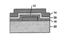
図6Aおよび図6Bを参照する。保護層28上に導電性の上側ワイヤ層14が配置される(図2のステップ32)。上側ワイヤ層14は、導電性の金属あるいはドープ半導体材料から形成されることができる。たとえば、一実施形態では、上側ワイヤ層14は、チタン層(〜5nm厚)およびその上のアルミニウム層(〜0.01ないし0.1μm厚)から形成される。上側ワイヤ層14は、従来の薄膜堆積プロセスによって堆積されることができる。従来の薄膜堆積プロセスは、物理的薄膜堆積プロセス(たとえば、マグネトロンスパッタリングまたは電子ビーム堆積)あるいは化学的薄膜堆積プロセス(たとえば、化学気相成長)を含む。
Please refer to FIG. 6A and FIG. 6B. A conductive
上側ワイヤ層14は、パターニングされたリフトオフ層を保護層に配置し、導電層をリフトオフ層上に堆積し、保護層28が概ね不溶性である溶媒でリフトオフ層を溶解することにより、パターニングされることができる。リフトオフ層は、ポリマー(たとえば、PMMA(ポリメチルメタクリレート))から形成され、電子ビームリソグラフィあるいはインプリンティングリソグラフィによってパターニングされることができる。その他、リフトオフ層は、従来のフォトレジストから形成され、従来のリソグラフィ技法(たとえば、光リソグラフィ)によってパターニングされることができる。結果として形成される上側ワイヤ層14は、約1nm〜数μmの範囲の幅寸法を有することができる。保護層28は、分子層16を完全に覆い、剥離溶媒において概ね不溶性である。従って保護層28は、剥離溶媒が侵入しないよう分子層16を封印し保護する。さもなければ、剥離溶媒が侵入することにより、分子層16が劣化するか、または完全に破壊されるであろう。
The
図7Aおよび図7Bに示されるように、導電性ワイヤ14は、保護層28の選択された領域をエッチングする(たとえば、反応性イオンエッチングによる)ことにより、他のデバイスから分離することができる(図2のステップ35)。詳細には、保護層28が電気導体から形成される実施形態では、上側ワイヤ層14を包囲する領域は、分子電子デバイスを他のデバイスから分離するためにエッチングして除去されることができる。
As shown in FIGS. 7A and 7B, the
図8Aおよび図8Bに示されるように、いくつかの実施形態では、保護層28の1つあるいは複数の選択された領域が、1つの導電タイプから別の導電タイプに変換され、分子電子デバイスを完成することができる(図2のステップ36)。たとえば、保護層28が電気導体から形成される実施形態では、分離保護領域38が絶縁体に変換され、分子電子デバイス10が他のデバイスからさらに分離される。たとえば、保護層28が金属(たとえば、アルミニウムあるいはチタンのような金属)から形成される場合には、分離保護領域38は、従来の酸化プロセスによって金属酸化物絶縁体に変換されることができる。別の実施形態では、保護層28は絶縁体から形成されることができ、上側ワイヤ層14と下側ワイヤ層12との間に配置されるデバイス保護領域40は電気導体に変換され、分子電子デバイスのデバイス領域が完成される。たとえば、保護層28は絶縁性アンチヒューズ構造から形成され、デバイス保護領域40は、上側ワイヤ層14と下側ワイヤ層16との間に、アンチヒューズ構造を溶断するほどの十分な電圧を印加することにより、電気導体に変換されることができる。アンチヒューズ構造を溶断するために必要とされる閾値電流は、分子層16の電流許容範囲内にある。別の例示では、保護層28は酸化物(たとえば、金属酸化物あるいは半導体酸化物)から形成されることができ、デバイス保護領域40は、デバイス保護領域40への上側ワイヤ層14の金属拡散によって電気導体に変換されることができる。この例示的な実施形態では、適当なオーミックコンタクト形成プロセスを用いて、デバイス保護領域40を電気導体に変換することができる。
As shown in FIGS. 8A and 8B, in some embodiments, one or more selected regions of the
結果として形成される分子電子デバイス10は、約50オングストローム〜10μmの横方向寸法を有することができる。
The resulting molecular
図9Aおよび図9Bを参照すると、別の実施形態では、上側ワイヤ層14が保護層28から形成される。この実施形態では、保護層28のある領域が、1つの導電タイプから別の導電タイプに変換され、上側ワイヤ層14が形成される。たとえば、一実施形態では、保護層28を電気導体(たとえば、アルミニウムあるいはチタン)から形成し、分離保護領域42を従来の酸化プロセスによって絶縁体に変換することによりその分子電子デバイスを他のデバイスから分離する。別の実施形態では、保護層28は絶縁体(たとえば、電気的アンチヒューズ構造)から形成され、その場合に、デバイス保護領域40が電気導体に変換されることにより分子電子デバイスのデバイス領域が完成される。
With reference to FIGS. 9A and 9B, in another embodiment, the
分子層16のために選択される分子あるいは材料に応じて、分子電子デバイス10は、種々の異なる電気的スイッチング機能のうちの任意のものを示すことができる。この電気的スイッチング機能は、下側ワイヤ層12および上側ワイヤ層14の接続あるいは切断を制御するために用いることができるものである。分子電子デバイスは、個々に構成可能あるいは構成変更可能にすることができる。個々に構成可能な実施形態では、分子電子デバイス10の初期状態は開いているか、閉じているかのいずれかにすることができる。ある特定の閾値電圧よりも高い電圧で分子電子デバイス10にバイアスをかけることにより、アクティブ材料あるいは分子18が、酸化あるいは還元され、デバイスの初期状態が永久に反転され、それによりデバイスのスイッチング状態を不可逆的に閉じるか、開くことができる。構成変更可能な実施形態では、スイッチングデバイスを何度も開閉することができる。スイッチングデバイスの開閉は、適当な閾値を越えるように印加電圧の極性および大きさを入れ替えることにより行われる。この適当な閾値は、アクティブ材料あるいは分子18を可逆的に酸化および還元するように選択される。
Depending on the molecule or material selected for the
一般的に、下側ワイヤ層12と上側ワイヤ層14との間に形成される電気的接続のタイプは、ワイヤ層12、14および分子層16が形成される材料に依存する。表1は、異なるデバイス材料の組み合わせから得られる種々のタイプの電気的スイッチング機能を明らかにする。

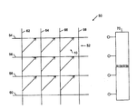
図10を参照すると、一実施形態では、分子電子デバイス10は、多数の行および多数の列に配列される複数のメモリセル52を含む抵抗性分子ワイヤ・クロスバーメモリ50内に実装されることができる。各メモリセル52は、個々の下側ワイヤ線54、56、58、60と個々の上側ワイヤ線62、64、66、68との間に結合される分子電子デバイス10を含む。メモリセルに印加される電圧は、そのメモリセルがその間に結合される下側ワイヤ線と上側ワイヤ線とに印加される電圧によって決定される。制御回路70が、メモリセルアレイ50内の1つあるいは複数のメモリセル52をアドレス指定(選択)し、その中に情報を書き込み、さらにそこから情報を読み出すように構成される。分子電子デバイス10は、下側ワイヤ線と上側ワイヤ線との間に挟まれる分子18を電気化学的に還元あるいは酸化することにより起動される。
Referring to FIG. 10, in one embodiment, the molecular
この実施形態では、分子層16の分子は、スイッチが相対的に高い電圧で酸化され、その状態が低い電圧で読み出されることができるように、ボルタモグラムにおいて大きなヒステリシスを有するように選択される。スイッチが(電気化学的に)閉じられるとき、接続しているワイヤ間の抵抗は低抵抗であり、それは、「1」の論理レベルに対応することができる。スイッチが開かれるとき、抵抗は高抵抗であり、それは「0」の論理レベルに対応することができる。抵抗性分子クロスバーメモリの動作に関するさらに細かい点は、米国特許第6,128,214号から得ることができる。
In this embodiment, the molecules of the
他の実施形態も特許請求の範囲内にある。たとえば、抵抗性分子ワイヤ・クロスバーメモリのほかに、他の分子ワイヤ・クロスバーメモリの実施形態が、表1において明らかにされる他のスイッチング機能のうちの任意の1つを提供するように構成される分子電子デバイスのアレイを含むことができる。さらに、上記の分子電子デバイスは、1つあるいは複数の論理(メモリではない)機能を実行するように設計される回路内に実装されることもできる。さらに他の実施形態も特許請求の範囲内にある。 Other embodiments are within the scope of the claims. For example, in addition to the resistive molecular wire crossbar memory, other molecular wire crossbar memory embodiments provide any one of the other switching functions identified in Table 1. An array of constructed molecular electronic devices can be included. Furthermore, the molecular electronic device described above can also be implemented in a circuit designed to perform one or more logic (not memory) functions. Still other embodiments are within the scope of the claims.
10 分子電子デバイス
12 下側ワイヤ層
14 上側ワイヤ層
16 分子層
18 分子
20 基板
28 保護層
38 分離保護領域
40 デバイス保護領域
42 分離保護領域
50 抵抗性分子ワイヤ・クロスバーメモリ
52 メモリセル
54〜60 下側ワイヤ線
62〜68 上側ワイヤ線
70 制御回路
DESCRIPTION OF
Claims (20)
下側ワイヤ層と、
デバイス領域において前記下側ワイヤ層上に配置される分子層と、
前記分子層上に配置され、電気導体領域および絶縁体領域を有する保護層とを含む分子電子デバイス。 A molecular electronic device,
A lower wire layer;
A molecular layer disposed on the lower wire layer in a device region;
A molecular electronic device comprising a protective layer disposed on the molecular layer and having an electrical conductor region and an insulator region.
下側ワイヤ層と、
デバイス領域において前記下側ワイヤ層上に配置される分子層と、
前記分子層上に配置され、電気導体領域および絶縁体領域を有する保護層とを含む分子メモリシステム。 A molecular memory system comprising an array of molecular electronic devices, each molecular electronic device comprising:
A lower wire layer;
A molecular layer disposed on the lower wire layer in a device region;
A molecular memory system comprising a protective layer disposed on the molecular layer and having an electrical conductor region and an insulator region.
The molecular memory system of claim 18, further comprising a patterned upper wire layer disposed on the protective layer.
Applications Claiming Priority (2)
| Application Number | Priority Date | Filing Date | Title |
|---|---|---|---|
| US09/815,922 US6707063B2 (en) | 2001-03-22 | 2001-03-22 | Passivation layer for molecular electronic device fabrication |
| PCT/US2002/008934 WO2002078056A2 (en) | 2001-03-22 | 2002-03-21 | Passivation layer for molecular electronic device fabrication |
Publications (2)
| Publication Number | Publication Date |
|---|---|
| JP2005509266A true JP2005509266A (en) | 2005-04-07 |
| JP2005509266A5 JP2005509266A5 (en) | 2005-12-22 |
Family
ID=25219185
Family Applications (1)
| Application Number | Title | Priority Date | Filing Date |
|---|---|---|---|
| JP2002575993A Pending JP2005509266A (en) | 2001-03-22 | 2002-03-21 | Protective layer for forming molecular electronic devices |
Country Status (5)
| Country | Link |
|---|---|
| US (2) | US6707063B2 (en) |
| EP (1) | EP1371063A2 (en) |
| JP (1) | JP2005509266A (en) |
| KR (1) | KR20030085015A (en) |
| WO (1) | WO2002078056A2 (en) |
Cited By (3)
| Publication number | Priority date | Publication date | Assignee | Title |
|---|---|---|---|---|
| JP2005521237A (en) * | 2001-06-28 | 2005-07-14 | ヒューレット・パッカード・カンパニー | Production of molecular electronic circuits by imprinting |
| JP2010506403A (en) * | 2006-10-03 | 2010-02-25 | ヒューレット−パッカード デベロップメント カンパニー エル.ピー. | Electrically operated switch |
| US8431921B2 (en) | 2009-01-13 | 2013-04-30 | Hewlett-Packard Development Company, L.P. | Memristor having a triangular shaped electrode |
Families Citing this family (16)
| Publication number | Priority date | Publication date | Assignee | Title |
|---|---|---|---|---|
| KR100470831B1 (en) * | 2002-05-20 | 2005-03-08 | 한국전자통신연구원 | Method for fabricating molecular electric devices |
| US7195343B2 (en) * | 2004-08-27 | 2007-03-27 | Lexmark International, Inc. | Low ejection energy micro-fluid ejection heads |
| US7242215B2 (en) * | 2004-10-27 | 2007-07-10 | Hewlett-Packard Development Company, L.P. | Nanoscale latches and impedance-encoded logic for use in nanoscale state machines, nanoscale pipelines, and in other nanoscale electronic circuits |
| US7443711B1 (en) | 2004-12-16 | 2008-10-28 | Hewlett-Packard Development Company, L.P. | Non-volatile programmable impedance nanoscale devices |
| US7741638B2 (en) | 2005-11-23 | 2010-06-22 | Hewlett-Packard Development Company, L.P. | Control layer for a nanoscale electronic switching device |
| US7302513B2 (en) * | 2006-04-03 | 2007-11-27 | Blaise Laurent Mouttet | Programmable crossbar signal processor |
| US8183554B2 (en) * | 2006-04-03 | 2012-05-22 | Blaise Laurent Mouttet | Symmetrical programmable memresistor crossbar structure |
| US9965251B2 (en) * | 2006-04-03 | 2018-05-08 | Blaise Laurent Mouttet | Crossbar arithmetic and summation processor |
| US20070231972A1 (en) * | 2006-04-03 | 2007-10-04 | Mouttet Blaise L | Manufacture of programmable crossbar signal processor |
| US20070233761A1 (en) * | 2006-04-03 | 2007-10-04 | Mouttet Blaise L | Crossbar arithmetic processor |
| US7576565B2 (en) * | 2006-04-03 | 2009-08-18 | Blaise Laurent Mouttet | Crossbar waveform driver circuit |
| US7763552B2 (en) * | 2006-04-28 | 2010-07-27 | Hewlett-Packard Development Company, L.P. | Method of interconnect formation using focused beams |
| US8030754B2 (en) | 2007-01-31 | 2011-10-04 | Hewlett-Packard Development Company, L.P. | Chip cooling channels formed in wafer bonding gap |
| WO2011010702A1 (en) * | 2009-07-22 | 2011-01-27 | 株式会社村田製作所 | Anti-fuse element |
| TW201330282A (en) * | 2012-01-09 | 2013-07-16 | Lextar Electronics Corp | Zener diode structure and manufacturing method thereof |
| CN103730302B (en) * | 2012-10-10 | 2016-09-14 | 清华大学 | Field emitting electronic source and field emission apparatus |
Family Cites Families (24)
| Publication number | Priority date | Publication date | Assignee | Title |
|---|---|---|---|---|
| JPS5679449A (en) | 1979-11-30 | 1981-06-30 | Mitsubishi Electric Corp | Production of semiconductor device |
| US4371883A (en) * | 1980-03-14 | 1983-02-01 | The Johns Hopkins University | Current controlled bistable electrical organic thin film switching device |
| JPH0669109B2 (en) * | 1984-12-07 | 1994-08-31 | シャ−プ株式会社 | Optical semiconductor device |
| US5272359A (en) * | 1988-04-07 | 1993-12-21 | California Institute Of Technology | Reversible non-volatile switch based on a TCNQ charge transfer complex |
| JPH02215173A (en) * | 1989-02-16 | 1990-08-28 | Canon Inc | Switching element and manufacture thereof |
| JPH02216173A (en) | 1989-02-17 | 1990-08-29 | Canon Inc | Cleaning device for image forming device |
| US5311039A (en) * | 1990-04-24 | 1994-05-10 | Seiko Epson Corporation | PROM and ROM memory cells |
| US5177567A (en) * | 1991-07-19 | 1993-01-05 | Energy Conversion Devices, Inc. | Thin-film structure for chalcogenide electrical switching devices and process therefor |
| US5350484A (en) | 1992-09-08 | 1994-09-27 | Intel Corporation | Method for the anisotropic etching of metal films in the fabrication of interconnects |
| US5834824A (en) | 1994-02-08 | 1998-11-10 | Prolinx Labs Corporation | Use of conductive particles in a nonconductive body as an integrated circuit antifuse |
| US5514876A (en) * | 1994-04-15 | 1996-05-07 | Trw Inc. | Multi-terminal resonant tunneling transistor |
| CN1106696C (en) * | 1994-05-16 | 2003-04-23 | 皇家菲利浦电子有限公司 | Semiconductor device provided with organic semiconductor material |
| US5424560A (en) * | 1994-05-31 | 1995-06-13 | Motorola, Inc. | Integrated multicolor organic led array |
| JP3683669B2 (en) * | 1997-03-21 | 2005-08-17 | 株式会社リコー | Semiconductor light emitting device |
| US6344662B1 (en) * | 1997-03-25 | 2002-02-05 | International Business Machines Corporation | Thin-film field-effect transistor with organic-inorganic hybrid semiconductor requiring low operating voltages |
| EP0968537B1 (en) * | 1997-08-22 | 2012-05-02 | Creator Technology B.V. | A method of manufacturing a field-effect transistor substantially consisting of organic materials |
| US6600185B1 (en) * | 1999-03-10 | 2003-07-29 | Oki Electric Industry Co., Ltd. | Ferroelectric capacitor with dielectric lining, semiconductor memory device employing same, and fabrication methods thereof |
| US6128214A (en) * | 1999-03-29 | 2000-10-03 | Hewlett-Packard | Molecular wire crossbar memory |
| US6265243B1 (en) * | 1999-03-29 | 2001-07-24 | Lucent Technologies Inc. | Process for fabricating organic circuits |
| US6459095B1 (en) * | 1999-03-29 | 2002-10-01 | Hewlett-Packard Company | Chemically synthesized and assembled electronics devices |
| US6314019B1 (en) * | 1999-03-29 | 2001-11-06 | Hewlett-Packard Company | Molecular-wire crossbar interconnect (MWCI) for signal routing and communications |
| DE10001301A1 (en) | 2000-01-14 | 2001-07-19 | Opel Adam Ag | Nut for mounting components in car has internal threaded section which is mounted in bore in component and upper section which can be deformed using special tool to form collar which fixes nut in place |
| US6541309B2 (en) | 2001-03-21 | 2003-04-01 | Hewlett-Packard Development Company Lp | Fabricating a molecular electronic device having a protective barrier layer |
| US6458621B1 (en) * | 2001-08-01 | 2002-10-01 | Hewlett-Packard Company | Batch fabricated molecular electronic devices with cost-effective lithographic electrodes |
-
2001
- 2001-03-22 US US09/815,922 patent/US6707063B2/en not_active Expired - Lifetime
-
2002
- 2002-03-21 WO PCT/US2002/008934 patent/WO2002078056A2/en active Application Filing
- 2002-03-21 KR KR10-2003-7012211A patent/KR20030085015A/en not_active Application Discontinuation
- 2002-03-21 JP JP2002575993A patent/JP2005509266A/en active Pending
- 2002-03-21 EP EP02713890A patent/EP1371063A2/en not_active Withdrawn
-
2003
- 2003-03-28 US US10/402,642 patent/US6835575B2/en not_active Expired - Lifetime
Cited By (7)
| Publication number | Priority date | Publication date | Assignee | Title |
|---|---|---|---|---|
| JP2005521237A (en) * | 2001-06-28 | 2005-07-14 | ヒューレット・パッカード・カンパニー | Production of molecular electronic circuits by imprinting |
| JP2010506403A (en) * | 2006-10-03 | 2010-02-25 | ヒューレット−パッカード デベロップメント カンパニー エル.ピー. | Electrically operated switch |
| US8766224B2 (en) | 2006-10-03 | 2014-07-01 | Hewlett-Packard Development Company, L.P. | Electrically actuated switch |
| US9735355B2 (en) | 2006-10-03 | 2017-08-15 | Hewlett Packard Enterprise Development Lp | Electrically actuated switch |
| US10374155B2 (en) | 2006-10-03 | 2019-08-06 | Hewlett Packard Enterprise Development Lp | Electrically actuated switch |
| US11283012B2 (en) | 2006-10-03 | 2022-03-22 | Hewlett Packard Enterprise Development Lp | Electrically actuated switch |
| US8431921B2 (en) | 2009-01-13 | 2013-04-30 | Hewlett-Packard Development Company, L.P. | Memristor having a triangular shaped electrode |
Also Published As
| Publication number | Publication date |
|---|---|
| US6835575B2 (en) | 2004-12-28 |
| KR20030085015A (en) | 2003-11-01 |
| WO2002078056A2 (en) | 2002-10-03 |
| US20030186466A1 (en) | 2003-10-02 |
| EP1371063A2 (en) | 2003-12-17 |
| US6707063B2 (en) | 2004-03-16 |
| WO2002078056A3 (en) | 2003-02-13 |
| US20020172064A1 (en) | 2002-11-21 |
Similar Documents
| Publication | Publication Date | Title |
|---|---|---|
| US6541309B2 (en) | Fabricating a molecular electronic device having a protective barrier layer | |
| JP2005509266A (en) | Protective layer for forming molecular electronic devices | |
| CN104659050B (en) | The top electrode barrier layer of RRAM device | |
| CN101395716B (en) | Nonvolatile storage element, nonvolatile storage device and method for manufacturing such element and device | |
| JP4643145B2 (en) | Electromechanical 3-trace junction device | |
| US6458621B1 (en) | Batch fabricated molecular electronic devices with cost-effective lithographic electrodes | |
| JP2002500430A (en) | Read only memory and read only memory device | |
| JP6901686B2 (en) | Switching elements, semiconductor devices and their manufacturing methods | |
| JP5135797B2 (en) | Switching element, switching element manufacturing method, rewritable logic integrated circuit, and memory element | |
| KR20160035582A (en) | Resistive memory device having field enhanced features | |
| KR20140092360A (en) | Memristive element based on hetero-junction oxide | |
| JP2008305889A (en) | Non-volatile storage device and method of manufacturing the same | |
| US20170186811A1 (en) | Compact Three-Dimensional Mask-Programmed Read-Only Memory | |
| KR100577544B1 (en) | Electrodes, method and apparatus for memory structure | |
| US6833593B2 (en) | Electrode means, a method for its manufacture, an apparatus comprising the electrode means as well as use of the latter | |
| JP2008218855A (en) | Nonvolatile storage element and manufacturing method thereof | |
| KR100473970B1 (en) | Memory element and method for production of a memory element | |
| KR100785032B1 (en) | Resistive random access memory device and method of manufacuring the same | |
| CN107706154A (en) | A kind of memory element, storage device, preparation method and driving method | |
| US10211258B2 (en) | Manufacturing methods of JFET-type compact three-dimensional memory | |
| JP2008147257A (en) | Electronic apparatus and method for manufacturing the same, and memory device | |
| KR101007562B1 (en) | Resistive memory device and method for manufacturing the same | |
| JP2001267552A (en) | Single-electron tunnel element |
Legal Events
| Date | Code | Title | Description |
|---|---|---|---|
| A521 | Request for written amendment filed |
Free format text: JAPANESE INTERMEDIATE CODE: A523 Effective date: 20050224 |
|
| A621 | Written request for application examination |
Free format text: JAPANESE INTERMEDIATE CODE: A621 Effective date: 20050224 |
|
| A977 | Report on retrieval |
Free format text: JAPANESE INTERMEDIATE CODE: A971007 Effective date: 20070622 |
|
| A131 | Notification of reasons for refusal |
Free format text: JAPANESE INTERMEDIATE CODE: A131 Effective date: 20070703 |
|
| A521 | Request for written amendment filed |
Free format text: JAPANESE INTERMEDIATE CODE: A523 Effective date: 20071002 |
|
| A131 | Notification of reasons for refusal |
Free format text: JAPANESE INTERMEDIATE CODE: A131 Effective date: 20071030 |
|
| A02 | Decision of refusal |
Free format text: JAPANESE INTERMEDIATE CODE: A02 Effective date: 20080610 |