JP2005341663A - Overcurrent detection device - Google Patents
Overcurrent detection device Download PDFInfo
- Publication number
- JP2005341663A JP2005341663A JP2004154341A JP2004154341A JP2005341663A JP 2005341663 A JP2005341663 A JP 2005341663A JP 2004154341 A JP2004154341 A JP 2004154341A JP 2004154341 A JP2004154341 A JP 2004154341A JP 2005341663 A JP2005341663 A JP 2005341663A
- Authority
- JP
- Japan
- Prior art keywords
- circuit
- load
- overcurrent detection
- overcurrent
- fet
- Prior art date
- Legal status (The legal status is an assumption and is not a legal conclusion. Google has not performed a legal analysis and makes no representation as to the accuracy of the status listed.)
- Pending
Links
- 238000001514 detection method Methods 0.000 title claims abstract description 53
- 230000010354 integration Effects 0.000 claims abstract description 5
- 101100464779 Saccharomyces cerevisiae (strain ATCC 204508 / S288c) CNA1 gene Proteins 0.000 abstract description 10
- 239000003990 capacitor Substances 0.000 description 4
- 238000010586 diagram Methods 0.000 description 4
- 238000009499 grossing Methods 0.000 description 2
- 238000001914 filtration Methods 0.000 description 1
- 238000007306 functionalization reaction Methods 0.000 description 1
- 230000020169 heat generation Effects 0.000 description 1
- 230000002265 prevention Effects 0.000 description 1
- 230000035945 sensitivity Effects 0.000 description 1
- 238000004804 winding Methods 0.000 description 1
Images
Classifications
-
- H—ELECTRICITY
- H03—ELECTRONIC CIRCUITRY
- H03K—PULSE TECHNIQUE
- H03K17/00—Electronic switching or gating, i.e. not by contact-making and –breaking
- H03K17/08—Modifications for protecting switching circuit against overcurrent or overvoltage
- H03K17/082—Modifications for protecting switching circuit against overcurrent or overvoltage by feedback from the output to the control circuit
- H03K17/0822—Modifications for protecting switching circuit against overcurrent or overvoltage by feedback from the output to the control circuit in field-effect transistor switches
-
- H—ELECTRICITY
- H02—GENERATION; CONVERSION OR DISTRIBUTION OF ELECTRIC POWER
- H02H—EMERGENCY PROTECTIVE CIRCUIT ARRANGEMENTS
- H02H3/00—Emergency protective circuit arrangements for automatic disconnection directly responsive to an undesired change from normal electric working condition with or without subsequent reconnection ; integrated protection
- H02H3/08—Emergency protective circuit arrangements for automatic disconnection directly responsive to an undesired change from normal electric working condition with or without subsequent reconnection ; integrated protection responsive to excess current
- H02H3/087—Emergency protective circuit arrangements for automatic disconnection directly responsive to an undesired change from normal electric working condition with or without subsequent reconnection ; integrated protection responsive to excess current for DC applications
-
- H—ELECTRICITY
- H03—ELECTRONIC CIRCUITRY
- H03F—AMPLIFIERS
- H03F1/00—Details of amplifiers with only discharge tubes, only semiconductor devices or only unspecified devices as amplifying elements
- H03F1/52—Circuit arrangements for protecting such amplifiers
-
- H—ELECTRICITY
- H03—ELECTRONIC CIRCUITRY
- H03F—AMPLIFIERS
- H03F2200/00—Indexing scheme relating to amplifiers
- H03F2200/462—Indexing scheme relating to amplifiers the current being sensed
Landscapes
- Engineering & Computer Science (AREA)
- Power Engineering (AREA)
- Emergency Protection Circuit Devices (AREA)
- Protection Of Static Devices (AREA)
- Control Of Voltage And Current In General (AREA)
Abstract
【課題】脈動電流を発生する負荷が接続されている場合やノイズ発生時等に、誤検出の発生を防止することができる過電流検出装置を提供する。
【解決手段】所定の負荷3に流れる過電流を検出する装置であって、入力信号を所定の基準値と比較する比較回路CMP1と、負荷3に流れる電流に対応する信号をフィルタリングし、これを入力信号として比較回路CMP1に与える、RC積分回路で構成されるフィルタ回路R4、C1を含む。特に、負荷3に直列的に接続された第1FET、及びこの第1FETに並列的に接続されて、負荷3に流れる電流に対応する信号をセンスソース端子Sから出力する第2FET、で構成されるマルチソースFET回路1と、センスソース端子Sとアースとの間に介接された過電流検出閾値抵抗R5とを含み、過電流検出閾値抵抗R5にかかる電圧をフィルタ回路を通して検出し、これを比較回路CMP1に与えるようにしている。
【選択図】図1An overcurrent detection device capable of preventing erroneous detection when a load generating pulsating current is connected or when noise is generated.
A device for detecting an overcurrent flowing through a predetermined load, comprising: a comparator circuit that compares an input signal with a predetermined reference value; and a signal corresponding to the current flowing through the load is filtered. Filter circuits R4 and C1 configured by an RC integration circuit are provided as input signals to the comparison circuit CMP1. In particular, the first FET is connected in series to the load 3 and the second FET is connected in parallel to the first FET and outputs a signal corresponding to the current flowing through the load 3 from the sense source terminal S. It includes a multi-source FET circuit 1 and an overcurrent detection threshold resistor R5 connected between the sense source terminal S and the ground. The voltage applied to the overcurrent detection threshold resistor R5 is detected through a filter circuit and compared. The signal is supplied to the circuit CMP1.
[Selection] Figure 1
Description
本発明は、所定の負荷に流れる過電流を検出する過電流検出装置に関し、特に、マルチソースFET回路を用いた過電流検出装置に関する。 The present invention relates to an overcurrent detection device that detects an overcurrent flowing through a predetermined load, and more particularly to an overcurrent detection device that uses a multi-source FET circuit.
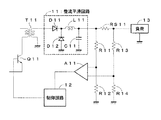
従来、ヒューズレスで関連する回路を保護するために、種々の過電流検出装置が提案されている。図2は、この種の従来の過電流検出装置を示す回路図である。 Conventionally, various overcurrent detection devices have been proposed to protect related circuits without a fuse. FIG. 2 is a circuit diagram showing this type of conventional overcurrent detection device.
図2において、トランスT11の2次巻線に励起された電圧は、ダイオードD11、D12、チョークコイルL11、コンデンサC11からなる整流平滑回路11により、直流電圧に変換されて負荷13に与えられる。負荷13に流れる電流に対応する、整流平滑回路11と負荷13との間に介接された電流検出抵抗RS11に発生する電圧は、分圧抵抗R11、R12、分圧抵抗R13、R14を介して、オペアンプA11に与えられる。
In FIG. 2, the voltage excited in the secondary winding of the transformer T11 is converted into a DC voltage by the rectifying /
オペアンプA11は、電流検出抵抗RS11に発生する電圧に応じた信号を制御回路12に帰還し、これに基づいて制御回路12がスイッチングトランジスタQ11のオンオフ比を制御することにより、負荷13に過電流が流れないようにしている。
The operational amplifier A11 feeds back a signal corresponding to the voltage generated in the current detection resistor RS11 to the
なお、このような先行技術文献情報としては次のものがある。
しかしながら、上述のような従来の過電流検出装置は、ヒューズレス化は達成するものの、過電流検出に電流検出抵抗RS11を用いているため、種々の問題が発生する。すなわち、負荷13に流れるピーク電流を検出することになるので、負荷13として、例えば、ホーン等のような脈動電流を発生する負荷が接続されている場合には、適正電流と過電流との判別ができず、誤検出が発生する。また、過電流閾値を超えるノイズが入力された場合にも、誤検出が発生する。更に、負荷13に直列的に電流検出抵抗RS11が接続しているため、発熱を引き起こす要因にもなる。
However, although the conventional overcurrent detection device as described above achieves fuse-less, various problems occur because the current detection resistor RS11 is used for overcurrent detection. That is, since the peak current flowing through the
よって本発明は、上述した現状に鑑み、脈動電流を発生する負荷が接続されている場合やノイズ発生時等にも、誤検出の発生を防止することができる過電流検出装置を提供することを課題としている。 Therefore, in view of the present situation described above, the present invention provides an overcurrent detection device capable of preventing the occurrence of false detection even when a load that generates a pulsating current is connected or when noise is generated. It is an issue.
上記課題を解決するためになされた請求項1記載の過電流検出装置は、所定の負荷に流れる過電流を検出する装置であって、前記過電流を検出するために、入力信号を所定の基準値と比較する比較回路と、前記負荷に流れる電流に対応する信号をフィルタリングし、これを前記入力信号として前記比較回路に与えるフィルタ回路と、を含むことを特徴とする。
The overcurrent detection device according to
請求項1記載の発明によれば、負荷に流れる電流に対応する信号をフィルタリングし、これを過電流を検出する比較回路の入力信号としている。これにより、ピーク電流ではなく、フィルタリングされた直流に近い入力信号が比較回路に与えられる。 According to the first aspect of the present invention, the signal corresponding to the current flowing through the load is filtered and used as the input signal of the comparison circuit for detecting the overcurrent. As a result, an input signal close to a filtered direct current, not a peak current, is given to the comparison circuit.
上記課題を解決するためになされた請求項2記載の過電流検出装置は、請求項1記載の過電流検出装置において、前記負荷に直列的に接続された第1FET、及び前記第1FETに並列的に接続されて、前記負荷に流れる電流に対応する信号をセンスソース端子から出力する第2FET、で構成されるマルチソースFET回路と、前記センスソース端子とアースとの間に介接された過電流検出閾値抵抗と、を含み、前記過電流検出閾値抵抗にかかる電圧を前記フィルタ回路を通して検出し、これを前記入力信号として前記比較回路に与える、ことを特徴とする。
The overcurrent detection device according to
請求項2記載の発明によれば、マルチソースFET回路のセンス端子とアースとの間に介接された過電流検出閾値抵抗と、を含み、過電流検出閾値抵抗にかかる電圧をフィルタ回路を通して検出し、これを入力信号として比較回路に与えるようにしている。 According to the second aspect of the present invention, the overcurrent detection threshold resistor connected between the sense terminal of the multi-source FET circuit and the ground is detected, and the voltage applied to the overcurrent detection threshold resistor is detected through the filter circuit. This is given as an input signal to the comparison circuit.
上記課題を解決するためになされた請求項3記載の過電流検出装置は、請求項1又は請求項2記載の過電流検出装置において、前記フィルタ回路をRCの積分回路で形成した、ことを特徴とする。
The overcurrent detection device according to
請求項3記載の発明によれば、フィルタ回路をRCの積分回路で形成しているので、接続される負荷に合わせたフィルタ定数を適宜設定することができる。 According to the third aspect of the present invention, since the filter circuit is formed by the RC integrating circuit, it is possible to appropriately set the filter constant according to the connected load.
請求項1記載の発明によれば、負荷に流れる電流に対応する信号をフィルタリングし、これを過電流を検出する比較回路の入力信号としている。これにより、ピーク電流ではなく、フィルタリングされた直流に近い入力信号が比較回路に与えられる。したがって、脈動電流を発生する負荷が接続されている場合やノイズ発生時にも、誤検出の発生を防止することができる。 According to the first aspect of the present invention, the signal corresponding to the current flowing through the load is filtered and used as the input signal of the comparison circuit for detecting the overcurrent. As a result, an input signal close to a filtered direct current, not a peak current, is given to the comparison circuit. Therefore, it is possible to prevent erroneous detection even when a load that generates a pulsating current is connected or when noise occurs.
請求項2記載の発明によれば、マルチソースFET回路のセンス端子とアースとの間に介接された過電流検出閾値抵抗と、を含み、過電流検出閾値抵抗にかかる電圧をフィルタ回路を通して検出し、これを入力信号として比較回路に与えるようにしている。したがって、誤検出の発生を防止できるうえに、発熱量も軽減できる。 According to the second aspect of the present invention, the overcurrent detection threshold resistor connected between the sense terminal of the multi-source FET circuit and the ground is detected, and the voltage applied to the overcurrent detection threshold resistor is detected through the filter circuit. This is given as an input signal to the comparison circuit. Therefore, occurrence of false detection can be prevented and the amount of generated heat can be reduced.
請求項3記載の発明によれば、フィルタ回路をRCの積分回路で形成しているので、接続される負荷に合わせたフィルタ定数を適宜設定することができる。したがって、適用範囲を広げることができる。 According to the third aspect of the present invention, since the filter circuit is formed by the RC integrating circuit, it is possible to appropriately set the filter constant according to the connected load. Therefore, the application range can be expanded.
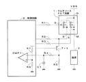
以下、本発明の実施の形態を図面に基づいて説明する。図1は、本発明の一実施形態に係る過電流検出装置を示す回路図である。 Hereinafter, embodiments of the present invention will be described with reference to the drawings. FIG. 1 is a circuit diagram showing an overcurrent detection apparatus according to an embodiment of the present invention.
図1に示すように、この過電流検出装置は、負荷3に接続されたマルチソースFET回路1、制御回路2、抵抗R4及びコンデンサC1からなるフィルタ回路を含んで構成される。
As shown in FIG. 1, the overcurrent detection device includes a filter circuit including a
マルチソースFET回路1は、詳しくは、電源VBBと負荷3との間に介接されている。マルチソースFET回路1は、メインソース端子Mに接続された負荷3に直列的に接続された第1FET、及びこの第1FETに並列的に接続されて、負荷3に流れる電流に対応する信号をセンスソース端子Sから出力する第2FET、で構成される。このような回路構成によると、センスソース端子Sからは、メインソース端子Mに接続された負荷3に流れる電流を分流して取り出すことができる。なお、Dはドレイン端子、Gはゲート端子、Kはケルビンソース端子を示す。
Specifically, the
マルチソースFET回路1のセンスソース端子S及びケルビンソース端子Kにはそれぞれ、抵抗R2及びR3が接続されている。センスソース端子Sと抵抗R2との間には、トランジスタTr1が並列的に接続され、そのコレクタ側とアースとの間には過電流検知閾値抵抗R5が介接されている。このコレクタ側及び抵抗R5の接続点と比較回路CMP1の入力端子との間には、フィルタ用抵抗R4及びフィルタ用コンデンサC1からなるフィルタ回路が接続されている。また、ゲート端子Gにはゲート抵抗R1が接続されている。
Resistors R2 and R3 are connected to the sense source terminal S and the Kelvin source terminal K of the
このように、マルチソースFET回路のセンス端子Sとアースとの間に過電流検出閾値抵抗R5を介接し、過電流検出閾値抵抗R5にかかる電圧を比較回路CMP1に与えるようにしているので、発熱量を大きく軽減できる。 As described above, the overcurrent detection threshold resistor R5 is connected between the sense terminal S of the multi-source FET circuit and the ground, and the voltage applied to the overcurrent detection threshold resistor R5 is applied to the comparison circuit CMP1. The amount can be greatly reduced.
制御回路2は、基準抵抗R6及びR7が基準端子に接続された過電流検出用の比較回路CMP1を含んで構成される。制御回路2は、例えば、IC化されており、図示しないチャージポンプ回路やドライバ回路を含んで構成するようにしてもよい。
The
このような構成において、センスソース端子Sから出力される負荷3に流れる電流に対応する電流は、トランジスタTr1のエミッタ側に出力される。トランジスタTr1がオンされると、そのコレクタ側に接続された過電流検出閾値抵抗R5にかかる電圧は、抵抗R4及びコンデンサC1からなるフィルタ回路を通して検出され、比較回路の入力端子に与えられる。そして、比較回路CMP1において、基準抵抗R6及びR7で分圧された基準端子にかかる基準電圧と比較されて、比較回路CMP1から比較結果に応じた制御信号が出力される。
In such a configuration, a current corresponding to the current flowing through the
この制御信号は、例えば、図2で示したように接続されたスイッチングトランジスタのオンオフ比を制御するために利用可能である。これにより、ヒューズレスで関連する回路を過電流から保護することができるようになる。 This control signal can be used, for example, to control the on / off ratio of the switching transistors connected as shown in FIG. As a result, it is possible to protect a related circuit from overcurrent without a fuse.
このように、負荷3に流れる電流に対応する信号をフィルタリングし、これを過電流を検出する比較回路CMP1の入力信号としているので、ピーク電流ではなく、フィルタリングされた直流に近い入力信号が比較回路CMP1に与えられることになる。したがって、脈動電流を発生する負荷が接続されている場合やノイズ発生時にも、誤検出の発生を防止することができる。
Thus, since the signal corresponding to the current flowing through the
特に、フィルタ回路をRCの積分回路で形成しているので、接続される負荷に合わせたフィルタ定数を適宜設定することができる。上述のように、直流に近い信号になるようにフィルタリングするのみならず、ピーク電流に近い電流も検出可能なように、RC時定数を変更して検出感度を上げることも可能である。したがって、フィルタ回路をRCの積分回路で形成することにより、この過電流検出装置の適用範囲を広げることができる。標準化促進の一助ともなる。 In particular, since the filter circuit is formed by an RC integration circuit, the filter constant can be set as appropriate according to the connected load. As described above, it is possible to increase the detection sensitivity by changing the RC time constant so as to detect not only a signal close to a direct current but also a current close to the peak current. Therefore, the application range of this overcurrent detection device can be expanded by forming the filter circuit with an RC integration circuit. It also helps to promote standardization.
また、比較回路CMP1の出力信号は、IC化された制御回路2の内部に出されるので、多機能化に適している。例えば、制御回路2内でロジックを組むことにより、過電流検出してから必要な時間だけ遅延させたり、所定のゲート入力と比較してから、過電流を示す制御信号を出力するというような誤検出防止機能を付加することも可能となる。
Further, since the output signal of the comparison circuit CMP1 is output inside the
以上のように、本発明の実施形態によれば、脈動電流を発生する負荷が接続されている場合やノイズ発生時等にも、誤検出の発生を防止することができる過電流検出装置を提供することができる。また、トランジスタ回路を用いているので、ヒューズレス、メンテナンスフリーであり、スペース効率もよいことはいうまでもない。 As described above, according to the embodiment of the present invention, there is provided an overcurrent detection device that can prevent erroneous detection even when a load that generates a pulsating current is connected or when noise is generated. can do. In addition, since a transistor circuit is used, it goes without saying that it is fuseless, maintenance-free, and has good space efficiency.
1 マルチソースFET回路
2 制御回路
3 負荷
R4、C1 フィルタ回路
1
Claims (3)
前記過電流を検出するために、入力信号を所定の基準値と比較する比較回路と、
前記負荷に流れる電流に対応する信号をフィルタリングし、これを前記入力信号として前記比較回路に与えるフィルタ回路と、
を含むことを特徴とする過電流検出装置。 A device for detecting an overcurrent flowing through a predetermined load,
A comparison circuit for comparing an input signal with a predetermined reference value in order to detect the overcurrent;
A filter circuit that filters a signal corresponding to a current flowing through the load and supplies the signal to the comparison circuit as the input signal;
An overcurrent detection device comprising:
前記負荷に直列的に接続された第1FET、及び前記第1FETに並列的に接続されて、前記負荷に流れる電流に対応する信号をセンスソース端子から出力する第2FET、で構成されるマルチソースFET回路と、
前記センスソース端子とアースとの間に介接された過電流検出閾値抵抗と、を含み、
前記過電流検出閾値抵抗にかかる電圧を前記フィルタ回路を通して検出し、これを前記入力信号として前記比較回路に与える、
ことを特徴とする過電流検出装置。 The overcurrent detection device according to claim 1,
A multi-source FET comprising: a first FET connected in series to the load; and a second FET connected in parallel to the first FET and outputting a signal corresponding to a current flowing through the load from a sense source terminal. Circuit,
An overcurrent detection threshold resistor interposed between the sense source terminal and the ground,
A voltage applied to the overcurrent detection threshold resistance is detected through the filter circuit, and this is supplied to the comparison circuit as the input signal;
An overcurrent detection device.
前記フィルタ回路をRCの積分回路で形成した、
ことを特徴とする過電流検出装置。 In the overcurrent detection device according to claim 1 or 2,
The filter circuit is formed by an RC integration circuit.
An overcurrent detection device.
Priority Applications (3)
| Application Number | Priority Date | Filing Date | Title |
|---|---|---|---|
| JP2004154341A JP2005341663A (en) | 2004-05-25 | 2004-05-25 | Overcurrent detection device |
| US11/135,390 US20060114633A1 (en) | 2004-05-25 | 2005-05-24 | Overcurrent detecting apparatus |
| EP05011269A EP1601104A1 (en) | 2004-05-25 | 2005-05-24 | Overcurrent detecting apparatus |
Applications Claiming Priority (1)
| Application Number | Priority Date | Filing Date | Title |
|---|---|---|---|
| JP2004154341A JP2005341663A (en) | 2004-05-25 | 2004-05-25 | Overcurrent detection device |
Publications (1)
| Publication Number | Publication Date |
|---|---|
| JP2005341663A true JP2005341663A (en) | 2005-12-08 |
Family
ID=34936896
Family Applications (1)
| Application Number | Title | Priority Date | Filing Date |
|---|---|---|---|
| JP2004154341A Pending JP2005341663A (en) | 2004-05-25 | 2004-05-25 | Overcurrent detection device |
Country Status (3)
| Country | Link |
|---|---|
| US (1) | US20060114633A1 (en) |
| EP (1) | EP1601104A1 (en) |
| JP (1) | JP2005341663A (en) |
Cited By (5)
| Publication number | Priority date | Publication date | Assignee | Title |
|---|---|---|---|---|
| JP2012054804A (en) * | 2010-09-02 | 2012-03-15 | Yazaki Corp | Protection device for load driving circuit |
| JP2013128343A (en) * | 2011-12-16 | 2013-06-27 | Auto Network Gijutsu Kenkyusho:Kk | Overcurrent protection circuit |
| JP2014158281A (en) * | 2014-04-23 | 2014-08-28 | Mitsubishi Electric Corp | Power module |
| US9007736B2 (en) | 2011-03-04 | 2015-04-14 | Mitsubishi Electric Corporation | Power module |
| JP2019068537A (en) * | 2017-09-29 | 2019-04-25 | Necプラットフォームズ株式会社 | Output device, protective apparatus, and setting method |
Families Citing this family (10)
| Publication number | Priority date | Publication date | Assignee | Title |
|---|---|---|---|---|
| JP2008537414A (en) | 2005-04-18 | 2008-09-11 | フリースケール セミコンダクター インコーポレイテッド | Adaptive protection circuit for power amplifier |
| DE102007038143A1 (en) * | 2007-08-13 | 2009-02-19 | Continental Automotive Gmbh | switching system |
| DE102010013322B4 (en) * | 2010-03-30 | 2011-11-17 | Austriamicrosystems Ag | Detection circuit and method for operating a detection circuit |
| TWI497682B (en) * | 2012-06-13 | 2015-08-21 | Elite Semiconductor Esmt | Integrated circuit having circuit damage protection mechanism and method thereof |
| US10041982B2 (en) | 2012-08-15 | 2018-08-07 | Texas Instruments Incorporated | Switch mode power converter current sensing apparatus and method |
| EP2746890B1 (en) * | 2012-12-19 | 2017-09-27 | Nxp B.V. | Current monitoring circuits and methods |
| JP6402591B2 (en) * | 2014-10-31 | 2018-10-10 | 富士電機株式会社 | Semiconductor device |
| JP6914867B2 (en) * | 2018-01-29 | 2021-08-04 | 株式会社東芝 | Driver circuit with overcurrent protection function |
| CN109660114B (en) * | 2019-02-26 | 2024-04-23 | 深圳英飞源技术有限公司 | Driving circuit of multipath parallel MOS (metal oxide semiconductor) tubes |
| US11831303B2 (en) * | 2020-12-08 | 2023-11-28 | Gan Systems Inc. | High accuracy current sensing for GaN power switching devices |
Family Cites Families (3)
| Publication number | Priority date | Publication date | Assignee | Title |
|---|---|---|---|---|
| US5018041A (en) * | 1989-06-16 | 1991-05-21 | National Semiconductor Corp. | Circuit for internal current limiting in a fast high side power switch |
| US5784244A (en) * | 1996-09-13 | 1998-07-21 | Cooper Industries, Inc. | Current limiting circuit |
| GB0110634D0 (en) * | 2001-05-01 | 2001-06-20 | Gunton Bruce S | Monitoring apparatus |
-
2004
- 2004-05-25 JP JP2004154341A patent/JP2005341663A/en active Pending
-
2005
- 2005-05-24 US US11/135,390 patent/US20060114633A1/en not_active Abandoned
- 2005-05-24 EP EP05011269A patent/EP1601104A1/en not_active Withdrawn
Cited By (5)
| Publication number | Priority date | Publication date | Assignee | Title |
|---|---|---|---|---|
| JP2012054804A (en) * | 2010-09-02 | 2012-03-15 | Yazaki Corp | Protection device for load driving circuit |
| US9007736B2 (en) | 2011-03-04 | 2015-04-14 | Mitsubishi Electric Corporation | Power module |
| JP2013128343A (en) * | 2011-12-16 | 2013-06-27 | Auto Network Gijutsu Kenkyusho:Kk | Overcurrent protection circuit |
| JP2014158281A (en) * | 2014-04-23 | 2014-08-28 | Mitsubishi Electric Corp | Power module |
| JP2019068537A (en) * | 2017-09-29 | 2019-04-25 | Necプラットフォームズ株式会社 | Output device, protective apparatus, and setting method |
Also Published As
| Publication number | Publication date |
|---|---|
| EP1601104A1 (en) | 2005-11-30 |
| US20060114633A1 (en) | 2006-06-01 |
Similar Documents
| Publication | Publication Date | Title |
|---|---|---|
| JP2005341663A (en) | Overcurrent detection device | |
| US5453904A (en) | Power control unit protection apparatus | |
| TW474059B (en) | A power factor correction circuit | |
| JP4200364B2 (en) | Switching type AC adapter circuit | |
| US6137696A (en) | Switching regulator for power converter with dual mode feedback input and method thereof | |
| CN101197534B (en) | Dc/dc converter | |
| US5610532A (en) | Isolated DC fault current sensor | |
| US6556401B1 (en) | Circuit arrangement for overload protection | |
| US20040070375A1 (en) | Step-down converter | |
| JP4729675B2 (en) | Switching mode power supply | |
| US7116140B2 (en) | Circuit arrangement for recognizing and outputting control signals, integrated circuit including the same, and use thereof | |
| JP5031491B2 (en) | Abnormality detection circuit for switching power supply circuit | |
| JP2010183721A (en) | Ac power supply detecting circuit and dc power supply unit | |
| JP4973724B2 (en) | Primary side control semiconductor integrated circuit and DC power supply | |
| JPH09505977A (en) | Voltage converter | |
| JP2006186479A (en) | Clamp circuit and semiconductor device having the same | |
| JPH04142468A (en) | Intelligent IC overcurrent detection circuit | |
| JPH1169789A (en) | Switching power supply device | |
| JP4329463B2 (en) | Capacitor charging circuit | |
| US6310331B1 (en) | Circuit configuration for driving an ignition coil | |
| KR100704589B1 (en) | Low voltage protection system of vehicle DC-AC inverter and its operation method | |
| JP3944109B2 (en) | Switching power supply | |
| JP2020137137A (en) | Clamp circuit | |
| JPS60141122A (en) | Output shortcircuit protecting circuit for power source circuit | |
| CN100524997C (en) | Undervoltage protection device |
Legal Events
| Date | Code | Title | Description |
|---|---|---|---|
| A621 | Written request for application examination |
Free format text: JAPANESE INTERMEDIATE CODE: A621 Effective date: 20061002 |
|
| A131 | Notification of reasons for refusal |
Free format text: JAPANESE INTERMEDIATE CODE: A131 Effective date: 20071211 |
|
| A02 | Decision of refusal |
Free format text: JAPANESE INTERMEDIATE CODE: A02 Effective date: 20080408 |