JP2005338366A - Antireflection film and optical component - Google Patents
Antireflection film and optical component Download PDFInfo
- Publication number
- JP2005338366A JP2005338366A JP2004156103A JP2004156103A JP2005338366A JP 2005338366 A JP2005338366 A JP 2005338366A JP 2004156103 A JP2004156103 A JP 2004156103A JP 2004156103 A JP2004156103 A JP 2004156103A JP 2005338366 A JP2005338366 A JP 2005338366A
- Authority
- JP
- Japan
- Prior art keywords
- film
- refractive index
- layer
- antireflection
- substrate
- Prior art date
- Legal status (The legal status is an assumption and is not a legal conclusion. Google has not performed a legal analysis and makes no representation as to the accuracy of the status listed.)
- Withdrawn
Links
Images


Classifications
-
- G—PHYSICS
- G02—OPTICS
- G02B—OPTICAL ELEMENTS, SYSTEMS OR APPARATUS
- G02B1/00—Optical elements characterised by the material of which they are made; Optical coatings for optical elements
- G02B1/10—Optical coatings produced by application to, or surface treatment of, optical elements
- G02B1/11—Anti-reflection coatings
- G02B1/113—Anti-reflection coatings using inorganic layer materials only
- G02B1/115—Multilayers
-
- G—PHYSICS
- G02—OPTICS
- G02C—SPECTACLES; SUNGLASSES OR GOGGLES INSOFAR AS THEY HAVE THE SAME FEATURES AS SPECTACLES; CONTACT LENSES
- G02C7/00—Optical parts
- G02C7/02—Lenses; Lens systems ; Methods of designing lenses
Landscapes
- Physics & Mathematics (AREA)
- Health & Medical Sciences (AREA)
- Ophthalmology & Optometry (AREA)
- General Physics & Mathematics (AREA)
- Optics & Photonics (AREA)
- General Health & Medical Sciences (AREA)
- Chemical & Material Sciences (AREA)
- Inorganic Chemistry (AREA)
- Surface Treatment Of Optical Elements (AREA)
Abstract
Description
本発明は、近赤外域、可視域で使用される光学レンズ等の光学部品に施される反射防止
膜、該反射防止膜を表面に形成した光学部品に関するものである。
The present invention relates to an antireflection film applied to an optical component such as an optical lens used in the near infrared region and the visible region, and an optical component having the antireflection film formed on the surface thereof.
一般に、レンズやプリズム等の光学部品の表面には、反射防止膜が施されている。この反射防止膜の主な目的は、多数の光学部品により構成される光学部品ユニットの透過率を向上すること、特に、可視域の反射を抑えることで、像の明るさや見え易さを向上させた光学機器とすることである。
近年、広い波長域で使用する光学機器が開発されている。これに用いる光学部品には、使用される波長域に対応した反射防止膜が用いられている。このような広い波長域に対応できる従来の反射防止膜は、例えば、特許文献1に記載されている。
この特許文献1に記載された発明の光学部品によれば、光学基板上に設けられた反射防止膜として、TiO2、SiO2、MgF2の3種類の材料を用いた8層構成とすることで、可視域から近赤外域として400nmから900nmの広帯域で0.8%以下の低反射率を実現している。
In recent years, optical devices used in a wide wavelength range have been developed. An optical component used for this uses an antireflection film corresponding to the wavelength range to be used. A conventional antireflection film that can cope with such a wide wavelength range is described in
According to the optical component of the invention described in
ここで、400nm〜900nmの帯域以上の広帯域で、低反射を必要とする光学機器、例えば、顕微鏡や内視鏡等の光学機器は、1つの光学系で可視域(400〜700nm)及び赤外域(700〜1000nm)での観察を行うため、光学系に用いるレンズは、可視域及び赤外域のそれぞれの波長範囲において反射防止作用を有する反射防止膜が施されたものが必要である。
上述した特許文献1記載の従来技術による反射防止膜を用いて、上述した条件でシュミレーションを行った場合、400nm〜1100nmの波長域の平均反射率は0.8%を越え、900nm〜1100nmの波長域における最大反射率は1.5%以上となる。従って、この反射防止膜を両面に施した光学基板1枚からなる光学部品での透過率は95%以下となり、光学基板5枚からなる光学部品での透過率は70%以下となる。
Here, a wide range of 400 nm to 900 nm or more, and an optical device that requires low reflection, for example, an optical device such as a microscope or an endoscope, has a visible range (400 to 700 nm) and an infrared range with a single optical system. In order to perform observation at (700 to 1000 nm), the lens used in the optical system needs to be provided with an antireflection film having an antireflection effect in each of the visible wavelength range and the infrared wavelength range.
When simulation is performed under the above-described conditions using the above-described conventional antireflection film described in
このため、光学部品を複数備える光学機器では、900nm〜1100nmの波長域の光量が不足するため赤外域での観察を行うことが困難であった。つまり、この反射防止膜は、400nm〜1100nmの波長域において可視域及び赤外域の同時観察を行う光学機器のレンズ等の反射防止膜として、対応させることが困難なものであった。 For this reason, in an optical apparatus provided with a plurality of optical components, it is difficult to perform observation in the infrared region because the light amount in the wavelength region of 900 nm to 1100 nm is insufficient. That is, this antireflection film has been difficult to be used as an antireflection film for lenses of optical instruments that perform simultaneous observation in the visible region and the infrared region in the wavelength range of 400 nm to 1100 nm.
この発明は、上記課題を考慮してなされたものであり、その目的は、可視域(400〜700nm)から赤外域(700〜1000nm)に亘る広帯域で、高い反射防止性能を有した反射防止膜及び該反射防止膜を光学基板上に備えて高い透過率を有し、400nm〜1100nmに亘る広帯域で使用可能な光学部品を提供することである。 The present invention has been made in consideration of the above problems, and its object is to provide an antireflection film having high antireflection performance over a wide band from the visible region (400 to 700 nm) to the infrared region (700 to 1000 nm). And providing an optical component having the antireflection film on an optical substrate and having a high transmittance and usable in a wide band ranging from 400 nm to 1100 nm.
上記の目的を達成するために、この発明は以下の手段を提供している。
請求項1に係る発明は、複数の層を有して光学基板上に設けられる反射防止膜であって、前記光学基板側から数えて第1、3、5及び7層に、屈折率が2.5以上3.1以下の高屈折率膜を成膜し、前記光学基板側から数えて第2、4、6及び8層に、屈折率が1.5以上1.8以下の中間屈折率膜と、屈折率が1.3以上1.5未満の低屈折率膜との少なくとも一方を成膜したものであり、前記各層の光学的膜厚nd(nは薄膜の屈折率、dは物理的膜厚)が、設計波長λに対して、第1層は(0.05〜0.25)×λ/4、第2層は(0.26〜1.1)×λ/4、第3層は(0.39〜0.68)×λ/4、第4層は(0.15〜0.40)×λ/4、第5層は(2.57〜2.76)×λ/4、第6層は(0.29〜0.47)×λ/4、第7層は(0.25〜0.42)×λ/4、第8層は(1.24〜1.28)×λ/4とした反射防止膜を提供する。
In order to achieve the above object, the present invention provides the following means.
The invention according to
この発明に係る反射防止膜においては、各層を構成する膜の屈折率及び物理的膜厚を限定することにより、可視域(400〜700nm)から赤外域(700から1100nm)で高い反射防止効果を得ることができる。
具体的には、400nmから1100nmの波長域で、0.5%以下の平均反射率を実現することができる。また、設計波長λを変えることにより、反射防止の波長域をシフトさせることが可能であり、また、長波長側の設計波長λ(例えば、520nmを600nm)とすることで反射防止の波長域を広げたりすることも可能である。
なお、光学基板の材質は、ガラス、結晶材料やプラスチック等を適用することができる。また、基板の形状は、平板形状、レンズ形状やプリズム形状等のあらゆる形状に適用可能である。また、成膜方法についても、スパッタリング法やイオンアシスト法等、特に限定されるものではない。
更に、(0.26〜1.1)×λ/4というのは、例えば、設計波長λを520nmとしたときに、第2層の光学的膜厚ndが(0.26〜1.1)×520nm/4=(0.26〜1.1)×130nm=33.8〜143nmとなることを意味するものである。また、他の層についても同様である。
In the antireflection film according to the present invention, by limiting the refractive index and the physical film thickness of the film constituting each layer, a high antireflection effect from the visible region (400 to 700 nm) to the infrared region (700 to 1100 nm) is obtained. Can be obtained.
Specifically, an average reflectance of 0.5% or less can be realized in a wavelength region from 400 nm to 1100 nm. Further, it is possible to shift the antireflection wavelength region by changing the design wavelength λ, and the antireflection wavelength region can be changed by setting the long wavelength side design wavelength λ (for example, 520 nm to 600 nm). It can also be expanded.
Note that glass, crystal material, plastic, or the like can be applied as the material of the optical substrate. Moreover, the shape of a board | substrate is applicable to all shapes, such as a flat plate shape, a lens shape, and a prism shape. Also, the film forming method is not particularly limited, such as a sputtering method or an ion assist method.
Furthermore, (0.26 to 1.1) × λ / 4 means that, for example, when the design wavelength λ is 520 nm, the optical film thickness nd of the second layer is (0.26 to 1.1). × 520 nm / 4 = (0.26 to 1.1) × 130 nm = 33.8 to 143 nm. The same applies to the other layers.
請求項2に係る発明は、請求項1記載の反射防止膜において、前記高屈折率膜、前記中間屈折率膜及び前記低屈折率膜の屈折率は、それぞれ350nm〜1100nmの波長域における屈折率である反射防止膜を提供する。
The invention according to
この発明に係る反射防止膜においては、低屈折率膜、中間屈折率膜及び高屈折率膜の各屈折率膜の屈折率の波長範囲を定めることで、400〜1100nmの波長域で高い反射防止効果を得ることができる。 In the antireflection film according to the present invention, by defining the wavelength range of the refractive index of each of the low refractive index film, the intermediate refractive index film, and the high refractive index film, high antireflection in the wavelength range of 400 to 1100 nm. An effect can be obtained.
請求項3に係る発明は、請求項1記載の反射防止膜において、前記高屈折率膜を構成する原料は、その主成分がTiOx(0<x<2)であり、Nb、Cr、Zr、Ta、Bi、Si、Ce、W、La及びALのうち少なくともいずれか1つ、若しくはこれらの酸化物、或いはこれらの混合物を用いて成膜された反射防止膜を提供する。 According to a third aspect of the present invention, in the antireflection film according to the first aspect, the main component of the high refractive index film is TiOx (0 <x <2), and Nb, Cr, Zr, Provided is an antireflection film formed using at least one of Ta, Bi, Si, Ce, W, La, and AL, or an oxide thereof, or a mixture thereof.
この発明に係る反射防止膜においては、400〜1100nmの波長域で高い反射防止効果を得ることができると共に、適当な膜を選択することにより、特定の波長域の反射率を低下させたものや、一定の波長帯域を拡大したものや、或いは、製造コストの低下が可能なもの等、その材料の特性を生かした反射防止膜を得ることができる。
また、高屈折率膜を構成する原料は、TiOx(0<x<2)に各元素、或いは、これらの酸化物や混合物を混合することで、屈折率2.5以上3.1以下の膜を得ることができる。なお、TiOxは、主成分として原料中に50重量%以上含まれるものである。
In the antireflection film according to the present invention, a high antireflection effect can be obtained in the wavelength range of 400 to 1100 nm, and by selecting an appropriate film, the reflectance in a specific wavelength range is reduced. In addition, an antireflection film can be obtained that makes use of the characteristics of the material, such as a film in which a certain wavelength band is expanded or a film whose manufacturing cost can be reduced.
The raw material constituting the high refractive index film is a film having a refractive index of 2.5 or more and 3.1 or less by mixing TiOx (0 <x <2) with each element, or an oxide or a mixture thereof. Can be obtained. TiOx is contained in the raw material as a main component in an amount of 50% by weight or more.
請求項4に係る発明は、請求項1記載の反射防止膜において、前記中間屈折率膜が、Al2O3、La2O5、CeF3、MgO、LaF3のいずれか1つ、又は、これらの混合物である反射防止膜を提供する。
The invention according to
この発明に係る反射防止膜においては、400〜1100nmの波長域で高い反射防止効果を得ることができると共に、適当な膜を選択することにより、特定の波長域の反射率を低下させたものや、一定の波長帯域を拡大したものや、或いは、製造コストの低下が可能なもの等、その材料の特性を生かした反射防止膜を得ることができる。
なお、中間屈折率膜として、安価な材料であるAl2O3を用いることが望ましい。
In the antireflection film according to the present invention, a high antireflection effect can be obtained in the wavelength range of 400 to 1100 nm, and by selecting an appropriate film, the reflectance in a specific wavelength range is reduced. In addition, an antireflection film can be obtained that makes use of the characteristics of the material, such as a film in which a certain wavelength band is expanded or a film whose manufacturing cost can be reduced.
As the intermediate refractive index film, it is desirable to use Al 2 O 3 which is an inexpensive material.
請求項5に係る発明は、請求項1記載の反射防止膜において、前記低屈折率膜が、SiO2、MgF2のいずれか1つ、又は、これらの混合物である反射防止膜を提供する。
The invention according to
この発明に係る反射防止膜においては、400〜1100nmの波長域で高い反射防止効果を得ることができると共に、適当な膜を選択することにより、特定の波長域の反射率を低下させたものや、一定の波長帯域を拡大したものや、或いは、製造コストの低下が可能なもの等、その材料の特性を生かした反射防止膜を得ることができる。
なお、第8層に、最も屈折率の低いMgF2を用いることが望ましい。
In the antireflection film according to the present invention, a high antireflection effect can be obtained in the wavelength range of 400 to 1100 nm, and by selecting an appropriate film, the reflectance in a specific wavelength range is reduced. In addition, an antireflection film can be obtained that makes use of the characteristics of the material, such as a film in which a certain wavelength band is expanded or a film whose manufacturing cost can be reduced.
Note that it is desirable to use MgF 2 having the lowest refractive index for the eighth layer.
請求項6に係る発明は、光学基板と、該光学基板上に設けられた請求項1から5のいずれか1項記載の反射防止膜とを有する光学部品を提供する。
The invention according to claim 6 provides an optical component comprising an optical substrate and the antireflection film according to any one of
この発明に係る光学部品においては、上述した反射防止膜を光学基板に設けることによって、400〜1100nmの波長域で、光学基板1面毎に反射率が下がり、面数が増加したときに透過率を上げることができる。 In the optical component according to the present invention, by providing the above-described antireflection film on the optical substrate, the transmittance decreases when the number of surfaces increases and the reflectance decreases for each surface of the optical substrate in the wavelength range of 400 to 1100 nm. Can be raised.
本発明に係る反射防止膜によれば、各層を構成する膜の屈折率及び膜厚を限定することにより、可視域(400〜700nm)から赤外域(700から1100nm)で高い反射防止効果を得ることができる。
また、本発明に係る光学部品によれば、400〜1100nmの波長域で高い透過率を得ることができる。
According to the antireflection film according to the present invention, a high antireflection effect is obtained from the visible region (400 to 700 nm) to the infrared region (700 to 1100 nm) by limiting the refractive index and film thickness of the film constituting each layer. be able to.
Moreover, according to the optical component which concerns on this invention, a high transmittance | permeability can be obtained in the wavelength range of 400-1100 nm.
次に、本発明に係る反射防止膜及び光学部品の第1実施形態を、図1から図5を参照して説明する。
本実施形態では、図1に示すイオンアシスト蒸着装置1により、基板(光学基板)2上に反射防止膜をイオンアシスト蒸着で成膜させる場合を例にして説明する。
この反射防止膜は、基板2側から数えて第1、3、5及び7層に、屈折率が2.5以上3.1以下の高屈折率膜を成膜し、基板2側から数えて第2、4、6及び8層に、屈折率が1.5以上1.8以下の中間屈折率膜と、屈折率が1.3以上1.5未満の低屈折率膜との少なくとも一方を成膜したものであり、各層の光学的膜厚nd(nは薄膜の屈折率、dは物理的膜厚)が、設計波長λに対して、第1層は(0.05〜0.25)×λ/4、第2層は(0.26〜1.1)×λ/4、第3層は(0.39〜0.68)×λ/4、第4層は(0.15〜0.40)×λ/4、第5層は(2.57〜2.76)×λ/4、第6層は(0.29〜0.47)×λ/4、第7層は(0.25〜0.42)×λ/4、第8層は(1.24〜1.28)×λ/4とされている。これらについては、以下に詳細に説明する。
Next, a first embodiment of an antireflection film and an optical component according to the present invention will be described with reference to FIGS.
In the present embodiment, an example in which an antireflection film is formed on a substrate (optical substrate) 2 by ion-assisted vapor deposition using the ion-assisted
This antireflection film is formed by forming a high refractive index film having a refractive index of 2.5 or more and 3.1 or less on the first, third, fifth and seventh layers from the
上記イオンアシスト蒸着装置1は、図1に示すように、右側面に排気口3、左側面にガス導入口4を有した真空チャンバ5を備えている。排気口3は、真空チャンバ5内を排気するものであり、ガス導入口4は、成膜中にO2ガスを真空チャンバ5内に導入するものである。また、真空チャンバ5の底部には、坩堝6a、6b、電子銃7a、7b、シャッタ8a、8b及びイオンガン9が設けられている。
As shown in FIG. 1, the ion-assisted
上記坩堝6a、6bは、内部に蒸着材料(膜を形成するための原料)を保持している。上記電子銃7a、7bは、電子ビームを坩堝6a、6bに照射して、該坩堝6a、6bの内部に保持されている蒸着材料を蒸発させるようになっている。上記シャッタ8a、8bは、各坩堝6a、6bの上方に開閉可能に配されており、開閉動作されることで、成膜の開始及び終了を行うようになっている。上記イオンガン9は、真空チャンバ5の中央上部に設けられたドーム10に設置された後述するヤトイ11内の上記基板2に向かってイオンを照射させるようになっている。
The
上記ドーム10は、上述したように基板2を入れたヤトイ11が設置可能とされ、成膜中は回転するようになっている。また、真空チャンバ5上部には、クリスタル監視計12と光学監視計13とが設けられている。クリスタル監視計12は、クリスタル基板14に成膜される物理的膜厚及び成膜速度を測定するものであり、光学監視計13は、成膜中のモニターガラス15の反射率変化を測定するようになっている。
As described above, the
このように構成されたイオンアシスト蒸着装置1により、真空チャンバ5内を8.0×10⁻³まで排気した後、基板2上に反射防止膜を成膜した。
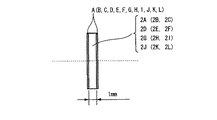
なお、本実施形態では、基板2として基板屈折率が1.52のS−BSL7((株)オハラ製)基板2A、基板屈折率が1.609のS−BSM14((株)オハラ製)基板2B、基板屈折率が1.721のS−LAL8((株)オハラ製)基板2Cの3種類を用い、それぞれ交換して3回に分けて各基板2A、2B、2C上に、各基板屈折率に基づいてそれぞれに反射防止膜A、B、Cを成膜した。
After the
In this embodiment, the
この際、設計波長λを520nm(即ち、高屈折率膜、中間屈折率膜及び低屈折率膜の屈折率が、それぞれ350nm〜1100nmの波長域における屈折率とされている)として、それぞれ基板2側から第1、3、5、7層に高屈折率膜としてTiO1.9とNb2O5との混合物(重量比95:5)を原料としてチタン、ニオブ混合酸化膜を、第2、4、6層に低屈折率膜としてSiO2を、第8層に低屈折率膜としてMgF2を用いて、表1に示す光学的膜厚nd(設計波長における膜の屈折率×物理的膜厚)で成膜した。 At this time, the design wavelength λ is set to 520 nm (that is, the refractive indexes of the high refractive index film, the intermediate refractive index film, and the low refractive index film are set to the refractive indexes in the wavelength range of 350 nm to 1100 nm, respectively). The first, third, fifth, and seventh layers from the side are titanium, niobium mixed oxide films using a mixture of TiO 1.9 and Nb 2 O 5 (weight ratio 95: 5) as a high refractive index film, Using SiO 2 as the low refractive index film for the 4th and 6th layers and MgF 2 as the low refractive index film for the 8th layer, the optical film thickness nd shown in Table 1 (refractive index of the film at the design wavelength × physical film) (Thickness).

成膜後の各層の屈折率は、520nmの波長において、高屈折率膜が2.53(上述した屈折率2.5以上3.1以下の範囲内)、低屈折率膜が1.46及び1.37(上述した屈折率1.3以上1.5未満の範囲内)の屈折率であった。
また、表1に示すように、各層の光学的膜厚ndは、上述した範囲内に設定されている。
The refractive index of each layer after the film formation is 2.53 for the high refractive index film (within the above-described refractive index of 2.5 to 3.1), 1.46 for the low refractive index film at a wavelength of 520 nm. The refractive index was 1.37 (within the above-described refractive index of 1.3 or more and less than 1.5).
Further, as shown in Table 1, the optical film thickness nd of each layer is set within the above-described range.
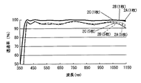
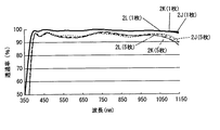
ここで、図2に、本実施形態の8層反射防止膜A、B、Cを片面に成膜した上記基板2A、2B、2Cの8層反射防止膜のみの分光反射率特性を示す。図2に示すように、いずれの基板2A、2B、2Cの反射防止膜A、B、Cも400nm〜700nmの波長域における反射率が、0.7%以下であり、また、平均反射率は、400nm〜1100nmで0.45%以下、400nm〜1150nmでも0.45%以下と低く、良好な反射防止性能を有している。
Here, FIG. 2 shows spectral reflectance characteristics of only the eight-layer antireflection films of the
上述したように、400nm〜1100nmまで、更には、400nm〜1150nmの波長域において、高い反射防止効果を持つ反射防止膜A、B、Cを得ることができた。
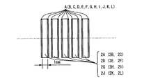
ここで、表1に示す反射防止膜Aを、両面に施した平面の基板2Aが1枚のものを図3に示し、基板2Aが5枚のものを図4に示す。
屈折率が1.52の基板2Aを、図3に示すように1枚配置した時と、図4に示すように5枚配置した時との分光透過率を測定した。また、同様に、屈折率1.609、1.721の基板2B、2Cについても分光透過率を測定した。この測定による分光透過率特性を、図5に示す。図5に示すように、400nm〜1100nmの波長域における透過率は、基板が1枚で98%以上、基板が5枚で94%以上となり、光学部品として共に可視域から赤外域に亘る広帯域で良好な透過率を示した。
As described above, antireflection films A, B, and C having a high antireflection effect could be obtained in the wavelength range of 400 nm to 1100 nm and further in the wavelength range of 400 nm to 1150 nm.
Here, FIG. 3 shows a single
Spectral transmittance was measured when one
なお、本実施形態の反射防止膜A、B、Cは、イオンアシスト蒸着により形成されたが、これに限定されるものではなく、スパッタリング法によっても同等の特性を得ることができる。
また、本実施形態では、高屈折率膜はTiOx(x=1.9)とNb2O5との重量比95:5の混合物を原料として形成した混合酸化物膜、低屈折率膜がSiO2及びMgF2としたが、これに限定されるものではなく、TiOxにおいては、x=1.5〜1.9でも、TiOxとNb2O5との混合比が98:2〜80:20でも、同様の効果が得られた。
また、高屈折率膜として、主成分をTiOx(0<x<2)とし、Cr、Zr、Ta、Bi、Si、Ce、W、La及びAlのいずれか、或いは、その酸化物の混合物を原料とした混合酸化物膜、低屈折率膜として、SiO2、MgF2のいずれか又はこれらの混合物というように、各膜と同様な屈折率を持つ膜であれば、同等の特性を有する反射防止膜A、B、Cを得ることができる。
The antireflection films A, B, and C of the present embodiment are formed by ion-assisted deposition, but are not limited to this, and equivalent characteristics can be obtained by a sputtering method.
In this embodiment, the high refractive index film is a mixed oxide film formed using a mixture of TiOx (x = 1.9) and Nb 2 O 5 in a weight ratio of 95: 5 as a raw material, and the low refractive index film is
In addition, as a high refractive index film, the main component is TiOx (0 <x <2), and any of Cr, Zr, Ta, Bi, Si, Ce, W, La, and Al, or a mixture of oxides thereof. As long as the film has a refractive index similar to that of each film, such as a mixed oxide film as a raw material, a low refractive index film such as SiO 2 , MgF 2 or a mixture thereof, a reflection having equivalent characteristics The prevention films A, B, and C can be obtained.
次に、本発明に係る反射防止膜及び光学部品の第2実施形態を、図1、図3、図4、図6及び図7を参照して説明する。なお、この第2実施形態においては、第1実施形態における構成要素と同一の部分については、同一の符号を付しその説明を省略する。
本実施形態では、図1に示すイオンアシスト蒸着装置1を用いて、真空槽内を8.0×10⁻⁴まで排気した後、基板2上に反射防止膜を成膜した、
なお、本実施形態では、基板2として基板屈折率が1.609のS−BSM14((株)オハラ製)基板2D、基板屈折率が1.721のS−LAL8((株)オハラ製)基板2E、基板屈折率が1.818のS−LAH53((株)オハラ製)基板2Fの3種類を用い、それぞれ交換して3回に分けて各基板2D、2E、2F上に、各基板屈折率に基づいてそれぞれに反射防止膜D、E、Fを成膜した。
Next, a second embodiment of the antireflection film and the optical component according to the present invention will be described with reference to FIG. 1, FIG. 3, FIG. 4, FIG. In the second embodiment, the same components as those in the first embodiment are denoted by the same reference numerals, and the description thereof is omitted.
In the present embodiment, the ion-assisted
In this embodiment, the
また、第1実施形態と同様に設計波長λを520nmとして、それぞれ基板2側から第1、3、5、7層に高屈折率膜としてTiO1.95とBi2O3との混合物(重量比60:40)を原料としてチタン、ビスマス混合酸化膜を、第2、4、6層に中間屈折率膜としてAl2O3を、第8層に低屈折率膜としてMgF2を用いて、表2に示す光学的膜厚nd(設計波長における膜の屈折率×物理的膜厚)で成膜した。
Similarly to the first embodiment, the design wavelength λ is set to 520 nm, and a mixture (weight) of TiO 1.95 and Bi 2 O 3 as high refractive index films on the first, third, fifth, and seventh layers from the
成膜後の各層の屈折率は、520nmの波長において、高屈折率膜が2.53(上述した屈折率2.5以上3.1以下の範囲内)、中間屈折率膜が1.64(上述した屈折率1.5以上1.8以下の範囲内)、低屈折率膜が1.37の(上述した屈折率1.3以上1.5未満の範囲内)屈折率であった。 The refractive index of each layer after film formation is 2.53 for the high refractive index film (within the above-described refractive index of 2.5 to 3.1) and 1.64 for the intermediate refractive index film at a wavelength of 520 nm. The refractive index of the low refractive index film was 1.37 (within the above-described refractive index of 1.3 to less than 1.5).
ここで、図6に、本実施形態の8層反射防止膜D、E、Fを片面に成膜した上記基板2D、2E、2Fの8層反射防止膜のみの分光反射率特性を示す。図6に示すように、いずれの基板2D、2E、2Fの反射防止膜D、E、Fも400nm〜700nmの波長域における反射率が0.65%以下であり、また平均反射率は、400nm〜1100nmで0.42%以下、400nm〜1150nmで0.45%以下と低く、良好な反射防止性能を有している。 Here, FIG. 6 shows spectral reflectance characteristics of only the eight-layer antireflection films of the substrates 2D, 2E, and 2F on which the eight-layer antireflection films D, E, and F of the present embodiment are formed on one side. As shown in FIG. 6, the antireflection films D, E, and F of any of the substrates 2D, 2E, and 2F have a reflectance of 0.65% or less in the wavelength region of 400 nm to 700 nm, and the average reflectance is 400 nm. It has a low antireflection performance of 0.42% or less at ˜1100 nm and 0.45% or less at 400 nm to 1150 nm.
上述したように、400nm〜1100nmまで、更には、400nm〜1150nmの波長域において、高い反射防止効果を持つ反射防止膜D、E、Fを得ることができる。
ここで、表2に示す反射防止膜Dを、両面に施した平面の基板2D(屈折率1.609)を、図3に示すように1枚配置した時と、図4に示すように5枚配置した時との分光透過率を測定した。同様に、反射防止膜E、Fを両面に施した屈折率1.721、1.818の基板2E、2Fについても分光透過率を測定した。
この測定による分光透過率特性を、図7に示す。図7に示すように、400nm〜1100nmの波長域における透過率は、基板が1枚で98%以上、基板が5枚で94%以上となり、光学部品として共に可視域から赤外域に亘る広帯域で良好な透過率を示した。
As described above, the antireflection films D, E, and F having a high antireflection effect can be obtained in the wavelength range of 400 nm to 1100 nm, and further in the wavelength range of 400 nm to 1150 nm.
Here, when a single flat substrate 2D (refractive index of 1.609) provided with the antireflection film D shown in Table 2 on both sides is arranged as shown in FIG. 3, and as shown in FIG. Spectral transmittance was measured when the sheets were placed. Similarly, the spectral transmittance was also measured for the substrates 2E and 2F having refractive indexes of 1.721 and 1.818 having antireflection films E and F applied on both surfaces.
The spectral transmittance characteristics by this measurement are shown in FIG. As shown in FIG. 7, the transmittance in the wavelength range of 400 nm to 1100 nm is 98% or more for one substrate and 94% or more for five substrates, and both optical components have a wide band from the visible region to the infrared region. Good transmittance was shown.
なお、本実施形態の反射防止膜D、E、Fは、第1実施形態と同様に、イオンアシスト蒸着により形成されたが、これに限定されるものではなく、スパッタリング法によっても同等の特性を得ることができる。
また、本実施形態では、高屈折率膜はTiO1.95とBi2O3との60:40の混合物、中間屈折率膜がAl2O3、低屈折率膜がMgF2としたが、これに限定されるものではなく、TiOxにおいては、x=1.7〜1.98でも、重量比98:2〜50:50でも同等の効果が得られた。
また、高屈折率膜として、主成分をTiOx(0<x<2)とし、Nb、Cr、Zr、Ta、Si、Ce、W、La及びAlのいずれか、或いは、その酸化物の混合物を原料とした混合酸化物膜、中間屈折率膜として、Al2O3、La2O5、CeF3、LaF3、MgOのいずれか、又はこれらの混合物、低屈折率膜として、SiO2、MgF2のいずれか又はこれらの混合物というように、各膜と同様な屈折率を持つ膜であれば、同等の特性を有する反射防止膜D、E、Fを得ることができる。
但し、中間屈折率膜として、安価な材料であるAl2O3を用いることが望ましい。
The antireflection films D, E, and F of this embodiment are formed by ion-assisted vapor deposition as in the first embodiment. However, the present invention is not limited to this, and the same characteristics can be obtained by a sputtering method. Can be obtained.
In this embodiment, the high refractive index film is a 60:40 mixture of TiO 1.95 and Bi 2 O 3 , the intermediate refractive index film is Al 2 O 3 , and the low refractive index film is MgF 2 . However, the present invention is not limited to this, and in TiOx, the same effect was obtained even when x = 1.7 to 1.98 and weight ratio 98: 2 to 50:50.
In addition, as a high refractive index film, a main component is TiOx (0 <x <2), and Nb, Cr, Zr, Ta, Si, Ce, W, La and Al, or a mixture of oxides thereof are used. Mixed oxide film as raw material, intermediate refractive index film as Al 2 O 3 , La 2 O 5 , CeF 3 , LaF 3 , MgO, or a mixture thereof, as low refractive index film as SiO 2 , MgF The antireflection films D, E, and F having the same characteristics can be obtained as long as the film has a refractive index similar to that of each film, such as any one of 2 or a mixture thereof.
However, it is desirable to use Al 2 O 3 which is an inexpensive material as the intermediate refractive index film.
次に、本発明に係る反射防止膜及び光学部品の第3実施形態を、図1、図3、図4、図8及び図9を参照して説明する。なお、この第3実施形態においては、第1実施形態における構成要素と同一の部分については、同一の符号を付しその説明を省略する。
本実施形態では、図1に示すイオンアシスト蒸着装置1を用いて、真空槽内を8.0×10⁻³Paまで排気した後、基板2上に反射防止膜を成膜した。
なお、本実施形態では、基板2として基板屈折率が1.52のS−BSL7((株)オハラ製)基板2G、基板屈折率が1.609のS−BSM14((株)オハラ製)基板2H、基板屈折率が1.721のS−LAL8((株)オハラ製)基板2Iの3種類を用い、交換してそれぞれ3回に分けて各基板2G、2H、2I上に、各基板屈折率に基づいてそれぞれに反射防止膜G、H、Iを成膜した。
Next, a third embodiment of the antireflection film and the optical component according to the present invention will be described with reference to FIG. 1, FIG. 3, FIG. 4, FIG. In the third embodiment, the same components as those in the first embodiment are denoted by the same reference numerals, and the description thereof is omitted.
In the present embodiment, the interior of the vacuum chamber was evacuated to 8.0 × 10 −3 Pa using the ion-assisted
In this embodiment, the
また、第1実施形態と同様に設計波長λを520nmとして、それぞれ基板2側から第1、3、5、7層に高屈折率膜としてTiO1.5とWO3の混合物(重量比90:10)を原料としてチタン、タングステン混合酸化膜を、第2、4、6、8層に低屈折率膜としてMgF2を用いて、表3に示す光学的膜厚nd(設計波長における膜の屈折率×物理的膜厚)で成膜した。
Similarly to the first embodiment, the design wavelength λ is 520 nm, and a mixture of TiO 1.5 and WO 3 is used as a high refractive index film on the first, third, fifth, and seventh layers from the
成膜後の各層の屈折率は、520nmの波長において、高屈折率膜が2.53(上述した屈折率2.5以上3.1以下の範囲内)、低屈折率膜が1.37(上述した屈折率
1.3以上1.5未満の範囲内)の屈折率であった。
The refractive index of each layer after film formation is 2.53 for the high refractive index film (within the above-described refractive index of 2.5 to 3.1) and 1.37 for the low refractive index film at a wavelength of 520 nm. The refractive index was within the range of the above-mentioned refractive index of 1.3 or more and less than 1.5.
ここで、図8に、本実施形態の8層反射防止膜G、H、Iを片面に成膜した上記基板2G、2H、2Iの8層反射防止膜のみの分光反射率特性を示す。図8に示すように、いずれの基板2G、2H、2Iの反射防止膜G、H、Iも400nm〜700nmの波長域における反射率が0.6%以下であり、また平均反射率は、400nm〜1100nmで0.42%以下、400nm〜1200nmで0.5%以下と低く、良好な反射防止性能を有している。
Here, FIG. 8 shows spectral reflectance characteristics of only the eight-layer antireflection films of the
上述したように、400nm〜1100nmまで、更には、400nm〜1200nmの波長域において、高い反射防止効果を持つ反射防止膜G、H、Iを得ることができる。
ここで、表3に示す反射防止膜Gを、両面に施した平面の基板2G(屈折率が1.52)を、図3に示すように1枚配置した時と、図4に示すように5枚配置した時との分光透過率を測定した。同様に、反射防止膜H、Iを両面に施した屈折率1.609、1.721の基板2H、2Iについても分光透過率を測定した。
この測定による分光透過率特性を、図9に示す。図9に示すように、400nm〜1100nmの波長域における透過率は、基板が1枚で97%以上、基板が5枚で94%以上となり、光学部品として共に可視域から赤外域に亘る広帯域で良好な透過率を示した。
As described above, antireflection films G, H, and I having a high antireflection effect can be obtained in the wavelength range of 400 nm to 1100 nm, and further in the wavelength range of 400 nm to 1200 nm.
Here, when the
The spectral transmittance characteristics obtained by this measurement are shown in FIG. As shown in FIG. 9, the transmittance in the wavelength region of 400 nm to 1100 nm is 97% or more for one substrate and 94% or more for five substrates, and both optical components have a wide band from the visible region to the infrared region. Good transmittance was shown.
なお、本実施形態の反射防止膜G、H、Iは、第1実施形態と同様に、イオンアシスト蒸着により形成されたが、これに限定されるものではなく、スパッタリング法によっても同等の特性を得ることができる。
また、本実施形態では、高屈折率膜はTiOx(x=1.5)とWO3との混合膜、低屈折率膜はMgF2としたが、これに限定されるものではなく、例えば、高屈折率膜として主成分をTiOx(0<x<2)とし、Nb、Cr、Zr、Ta、Bi、Si、Ce、La及びAlのいずれか、或いは、その酸化物の混合物を原料とした混合酸化物膜、低屈折率膜としてSiO2、MgF2のいずれか又はこれらの混合物というように、各膜と同様な屈折率を持つ膜であれば、同等の特性を有する反射防止膜G、H、Iを得ることができる。
The antireflection films G, H, and I of the present embodiment are formed by ion-assisted deposition as in the first embodiment. However, the present invention is not limited to this, and the same characteristics can be obtained by a sputtering method. Can be obtained.
In the present embodiment, the high refractive index film is a mixed film of TiOx (x = 1.5) and WO 3 and the low refractive index film is MgF 2. However, the present invention is not limited to this. For example, The main component of the high refractive index film is TiOx (0 <x <2), and any of Nb, Cr, Zr, Ta, Bi, Si, Ce, La and Al, or a mixture of oxides thereof is used as a raw material. As long as the film has a refractive index similar to each film, such as a mixed oxide film, SiO 2 , MgF 2 or a mixture thereof as a low refractive index film, an antireflection film G having equivalent characteristics, H and I can be obtained.
次に、本発明に係る反射防止膜及び光学部品の第4実施形態を、図1、図3、図4、図10及び図11を参照して説明する。なお、この第4実施形態においては、第1実施形態における構成要素と同一の部分については、同一の符号を付しその説明を省略する。
本実施形態では、図1に示すイオンアシスト蒸着装置1を用いて、真空槽内を8.0×10⁻³Paまで排気した後、基板2上に反射防止膜を成膜した。
なお、本実施形態では、基板2として基板屈折率が1.609のS−BSM14((株)オハラ製)基板2J、基板屈折率が1.721のS−LAL8((株)オハラ製)基板2K、基板屈折率が1.818のS−LAH53((株)オハラ製)基板2Lの3種類を用い、それぞれ交換して3回に分けて各基板2J、2K、2Lに、各基板屈折率に基づいてそれぞれに反射防止膜J、K、Lを成膜した。
Next, a fourth embodiment of the antireflection film and the optical component according to the present invention will be described with reference to FIG. 1, FIG. 3, FIG. 4, FIG. In the fourth embodiment, the same components as those in the first embodiment are denoted by the same reference numerals, and the description thereof is omitted.
In the present embodiment, an antireflection film was formed on the
In this embodiment, the
また、第1実施形態と同様に、設計波長λを520nmとして、それぞれ基板2側から第1、3、5、7層に高屈折率膜としてTiOx(x=1.9)とNb2O5との混合物(重量比95:5)を原料としてチタン、ニオブ混合酸化膜を、第4層に中間屈折率膜としてAl2O3を、第6層に低屈折率膜としてSiO2を、第2、8層に低屈折率膜としてMgF2を用いて、表4に示す光学的膜厚nd(設計波長における膜の屈折率×物理的膜厚)で成膜した。
Similarly to the first embodiment, the design wavelength λ is 520 nm, and TiOx (x = 1.9) and Nb 2 O 5 are used as high refractive index films on the first, third, fifth, and seventh layers from the
成膜後の各層の屈折率は、520nmの波長において、高屈折率膜が2.53(上述した屈折率2.5以上3.1以下の範囲内)、中間屈折率膜が1.64(上述した屈折率1.5以上1.8以下の範囲内)、低屈折率膜が1.37(上述した屈折率1.3以上1.5未満の範囲内)の屈折率であった。 The refractive index of each layer after film formation is 2.53 for the high refractive index film (within the above-described refractive index of 2.5 to 3.1) and 1.64 for the intermediate refractive index film at a wavelength of 520 nm. The refractive index of the low refractive index film was 1.37 (within the above-described refractive index of 1.3 to less than 1.5).
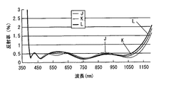
ここで、図10に、本実施形態の8層反射防止膜J、K、Lを片面に成膜した上記基板2J、2K、2Lの8層反射防止膜のみの分光反射率特性を示す。図10に示すように、いずれの基板2J、2K、2Lの反射防止膜J、K、Lも400nm〜700nmの波長域における反射率が0.55%以下であり、また平均反射率は400nm〜1100nmで0.43%以下、400nm〜1150nmで0.45%以下と低く、良好な反射防止性能を有している。
Here, FIG. 10 shows spectral reflectance characteristics of only the eight-layer antireflection films of the
上述したように、400nm〜1100nmまで、更には、400nm〜1150nmの波長域において、高い反射防止効果を持つ反射防止膜J、K、Lを得ることができる。
ここで、表4に示す反射防止膜Jを両面に施した平面の基板2J(屈折率1.609)を、図3に示すように1枚配置した時と、図4に示すように5枚配置した時との分光透過率を測定した。同様に、反射防止膜K、Lを両面に施した屈折率1.721、1.818の基板2K、2Lについても分光透過率を測定した。
この測定による分光透過率特性を、図11に示す。図11に示すように、400nm〜1100nmの波長域における透過率は、基板が1枚で98%以上、基板が5枚で93%以上となり、光学部品として共に可視域から赤外域に亘る広帯域で良好な透過率を示した。
As described above, the antireflection films J, K, and L having a high antireflection effect can be obtained in the wavelength range of 400 nm to 1100 nm, and further in the wavelength range of 400 nm to 1150 nm.
Here, when one
The spectral transmittance characteristics by this measurement are shown in FIG. As shown in FIG. 11, the transmittance in the wavelength range of 400 nm to 1100 nm is 98% or more for one substrate and 93% or more for five substrates, and both optical components have a wide band from the visible region to the infrared region. Good transmittance was shown.
なお、本実施形態の反射防止膜J、K、Lは、第1実施形態と同様に、イオンアシスト蒸着により形成されたが、これに限定されるものではなく、スパッタリング法によっても同等の特性を得ることができる。
また、本実施形態では、高屈折率膜はTiOx(x=1.9)とNb2O5との混合膜、中間屈折率膜はAl2O3、低屈折率膜はSiO2及びMgF2を用いたが、これに限定されるものではなく、例えば、高屈折率膜として、主成分をTiOx(0<x<2)とし、Cr、Zr、Ta、Bi、Si、Ce、W、La及びAlのいずれか、或いは、その酸化物との混合物を原料とした形成した混合膜、中間屈折率膜としてAl2O3、La2O5、CeF3、LaF3、MgOのいずれか、又はこれらの混合物、低屈折率膜としてSiO2、MgF2のいずれか又はこれらの混合物というように、各膜と同様な屈折率を持つ膜であれば、同等の特性を有する反射防止膜J、K、Lを得ることができる。
但し、中間屈折率膜として、安価な材料であるAl2O3 を用いることが好ましい。
The antireflection films J, K, and L of this embodiment are formed by ion-assisted vapor deposition as in the first embodiment. However, the present invention is not limited to this, and the same characteristics can be obtained by a sputtering method. Can be obtained.
In this embodiment, the high refractive index film is a mixed film of TiOx (x = 1.9) and Nb 2 O 5 , the intermediate refractive index film is Al 2 O 3 , and the low refractive index film is SiO 2 and MgF 2. However, the present invention is not limited to this. For example, as a high refractive index film, the main component is TiOx (0 <x <2), Cr, Zr, Ta, Bi, Si, Ce, W, La And any one of Al and Al, or a mixed film formed using a mixture of the oxide as a raw material, Al 2 O 3 , La 2 O 5 , CeF 3 , LaF 3 , MgO as an intermediate refractive index film, or Antireflection films J and K having the same characteristics as long as the film has a refractive index similar to that of each film, such as a mixture of these, a low refractive index film such as SiO 2 or MgF 2 , or a mixture thereof. , L can be obtained.
However, it is preferable to use Al 2 O 3 which is an inexpensive material as the intermediate refractive index film.
A、B、C、D、E、F、G、H、I、J、K、L 反射防止膜
2 基板(光学基板)
A, B, C, D, E, F, G, H, I, J, K,
Claims (6)
前記光学基板側から数えて第1、3、5及び7層に、屈折率が2.5以上3.1以下の高屈折率膜を成膜し、
前記光学基板側から数えて第2、4、6及び8層に、屈折率が1.5以上1.8以下の中間屈折率膜と、屈折率が1.3以上1.5未満の低屈折率膜との少なくとも一方を成膜したものであり、
前記各層の光学的膜厚nd(nは薄膜の屈折率、dは物理的膜厚)が、設計波長λに対して、第1層は(0.05〜0.25)×λ/4、第2層は(0.26〜1.1)×λ/4、第3層は(0.39〜0.68)×λ/4、第4層は(0.15〜0.40)×λ/4、第5層は(2.57〜2.76)×λ/4、第6層は(0.29〜0.47)×λ/4、第7層は(0.25〜0.42)×λ/4、第8層は(1.24〜1.28)×λ/4としたことを特徴とする反射防止膜。 An antireflection film provided on an optical substrate having a plurality of layers,
A high refractive index film having a refractive index of 2.5 or more and 3.1 or less is formed on the first, third, fifth and seventh layers counted from the optical substrate side,
An intermediate refractive index film having a refractive index of 1.5 or more and 1.8 or less and a low refractive index of 1.3 or more and less than 1.5 on the second, fourth, sixth and eighth layers counted from the optical substrate side. And at least one of the rate film is formed,
The optical film thickness nd (n is the refractive index of the thin film and d is the physical film thickness) of each of the layers is (0.05 to 0.25) × λ / 4 with respect to the design wavelength λ. The second layer is (0.26-1.1) × λ / 4, the third layer is (0.39-0.68) × λ / 4, and the fourth layer is (0.15-0.40) × λ / 4, the fifth layer is (2.57 to 2.76) × λ / 4, the sixth layer is (0.29 to 0.47) × λ / 4, and the seventh layer is (0.25 to 0). .42) × λ / 4, and the eighth layer is (1.24 to 1.28) × λ / 4.
前記高屈折率膜、前記中間屈折率膜及び前記低屈折率膜の屈折率は、それぞれ350nm〜1100nmの波長域における屈折率であることを特徴とする反射防止膜。 The antireflection film according to claim 1,
The antireflective film, wherein the high refractive index film, the intermediate refractive index film, and the low refractive index film each have a refractive index in a wavelength range of 350 nm to 1100 nm.
前記高屈折率膜を構成する原料は、その主成分がTiOx(0<x<2)であり、
Nb、Cr、Zr、Ta、Bi、Si、Ce、W、La及びALのうち少なくともいずれか1つ、若しくはこれらの酸化物、或いはこれらの混合物を用いて成膜されたことを特徴とする反射防止膜。 The antireflection film according to claim 1,
The raw material constituting the high refractive index film is mainly composed of TiOx (0 <x <2),
Reflective film formed using at least one of Nb, Cr, Zr, Ta, Bi, Si, Ce, W, La and AL, or an oxide thereof, or a mixture thereof. Prevention film.
前記中間屈折率膜が、Al2O3、La2O5、CeF3、MgO、LaF3のいずれか1つ、又は、これらの混合物であることを特徴とする反射防止膜。 The antireflection film according to claim 1,
The antireflective film, wherein the intermediate refractive index film is any one of Al 2 O 3 , La 2 O 5 , CeF 3 , MgO, LaF 3 , or a mixture thereof.
前記低屈折率膜が、SiO2、MgF2のいずれか1つ、又は、これらの混合物であることを特徴とする反射防止膜。 The antireflection film according to claim 1,
The antireflective film, wherein the low refractive index film is any one of SiO 2 and MgF 2 or a mixture thereof.
An optical component comprising: an optical substrate; and the antireflection film according to claim 1 provided on the optical substrate.
Priority Applications (1)
| Application Number | Priority Date | Filing Date | Title |
|---|---|---|---|
| JP2004156103A JP2005338366A (en) | 2004-05-26 | 2004-05-26 | Antireflection film and optical component |
Applications Claiming Priority (1)
| Application Number | Priority Date | Filing Date | Title |
|---|---|---|---|
| JP2004156103A JP2005338366A (en) | 2004-05-26 | 2004-05-26 | Antireflection film and optical component |
Publications (1)
| Publication Number | Publication Date |
|---|---|
| JP2005338366A true JP2005338366A (en) | 2005-12-08 |
Family
ID=35492029
Family Applications (1)
| Application Number | Title | Priority Date | Filing Date |
|---|---|---|---|
| JP2004156103A Withdrawn JP2005338366A (en) | 2004-05-26 | 2004-05-26 | Antireflection film and optical component |
Country Status (1)
| Country | Link |
|---|---|
| JP (1) | JP2005338366A (en) |
Cited By (16)
| Publication number | Priority date | Publication date | Assignee | Title |
|---|---|---|---|---|
| WO2010113622A1 (en) * | 2009-04-01 | 2010-10-07 | 東海光学株式会社 | Light-emitting member, plastic lens for glasses, and production method therefor |
| JP2011039218A (en) * | 2009-08-10 | 2011-02-24 | Seiko Epson Corp | Method for producing optical article |
| EP2128658A3 (en) * | 2008-05-22 | 2011-05-11 | Fujinon Corporation | Reflection reducing film, optical member and optical system |
| JP2011232569A (en) * | 2010-04-28 | 2011-11-17 | Seiko Epson Corp | Optical article and manufacturing method of the same |
| WO2011145613A1 (en) * | 2010-05-20 | 2011-11-24 | 東海光学株式会社 | Plastic optical product and plastic lens for eyeglasses |
| JP2012078829A (en) * | 2010-10-01 | 2012-04-19 | Carl Zeiss Vision Gmbh | Optical lens having antistatic coating |
| WO2012169393A1 (en) | 2011-06-10 | 2012-12-13 | オリンパス株式会社 | Antireflection film, optical system and optical device |
| WO2013179914A1 (en) | 2012-05-30 | 2013-12-05 | オリンパス株式会社 | Antireflection film, optical system, optical device and method for forming antireflection film |
| JP2017068096A (en) * | 2015-09-30 | 2017-04-06 | 株式会社トプコン | Antireflection film, optical element, and ophthalmic device |
| WO2018155213A1 (en) | 2017-02-27 | 2018-08-30 | 東海光学株式会社 | Plastic spectacle lens and spectacles |
| JP2019053115A (en) * | 2017-09-13 | 2019-04-04 | Agc株式会社 | Transparent base body with antireflection film and display device using the same |
| WO2021024834A1 (en) * | 2019-08-08 | 2021-02-11 | Hoya株式会社 | Antireflection film-equipped optical member and production method therefor |
| WO2023195500A1 (en) * | 2022-04-08 | 2023-10-12 | Agc株式会社 | Antireflection film-attached transparent substrate and image display device |
| WO2023195497A1 (en) * | 2022-04-08 | 2023-10-12 | Agc株式会社 | Antireflection film-equipped transparent substrate and image display device |
| WO2023195498A1 (en) * | 2022-04-08 | 2023-10-12 | Agc株式会社 | Anti-reflective film-attached transparent substrate and image display device |
| WO2024014442A1 (en) * | 2022-07-13 | 2024-01-18 | Agc株式会社 | Antireflection film-equipped transparent substrate and image display device |
-
2004
- 2004-05-26 JP JP2004156103A patent/JP2005338366A/en not_active Withdrawn
Cited By (28)
| Publication number | Priority date | Publication date | Assignee | Title |
|---|---|---|---|---|
| US8248699B2 (en) | 2008-05-22 | 2012-08-21 | Fujifilm Corporation | Reflection reducing film, optical member and optical system |
| EP2128658A3 (en) * | 2008-05-22 | 2011-05-11 | Fujinon Corporation | Reflection reducing film, optical member and optical system |
| JP2010243601A (en) * | 2009-04-01 | 2010-10-28 | Tokai Kogaku Kk | Optical member, plastic lens for glasses and method of manufacturing them |
| WO2010113622A1 (en) * | 2009-04-01 | 2010-10-07 | 東海光学株式会社 | Light-emitting member, plastic lens for glasses, and production method therefor |
| US8746878B2 (en) | 2009-04-01 | 2014-06-10 | Tokai Optical Co., Ltd. | Optical member, plastic lens for eyeglasses, and method for manufacturing the same |
| CN102369462A (en) * | 2009-04-01 | 2012-03-07 | 东海光学株式会社 | Light-emitting member, plastic lens for glasses, and production method therefor |
| JP2011039218A (en) * | 2009-08-10 | 2011-02-24 | Seiko Epson Corp | Method for producing optical article |
| JP2011232569A (en) * | 2010-04-28 | 2011-11-17 | Seiko Epson Corp | Optical article and manufacturing method of the same |
| US9022561B2 (en) | 2010-05-20 | 2015-05-05 | Tokai Optical Co., Ltd. | Plastic optical product and plastic lens for spectacles |
| JP2011242697A (en) * | 2010-05-20 | 2011-12-01 | Tokai Kogaku Kk | Plastic optical product and plastic lens for spectacles |
| WO2011145613A1 (en) * | 2010-05-20 | 2011-11-24 | 東海光学株式会社 | Plastic optical product and plastic lens for eyeglasses |
| JP2012078829A (en) * | 2010-10-01 | 2012-04-19 | Carl Zeiss Vision Gmbh | Optical lens having antistatic coating |
| WO2012169393A1 (en) | 2011-06-10 | 2012-12-13 | オリンパス株式会社 | Antireflection film, optical system and optical device |
| JP2012255984A (en) * | 2011-06-10 | 2012-12-27 | Olympus Corp | Antireflection film, optical system and optical apparatus |
| US9423529B2 (en) | 2011-06-10 | 2016-08-23 | Olympus Corporation | Antireflection coating, optical system, and optical instrument |
| WO2013179914A1 (en) | 2012-05-30 | 2013-12-05 | オリンパス株式会社 | Antireflection film, optical system, optical device and method for forming antireflection film |
| JP2017068096A (en) * | 2015-09-30 | 2017-04-06 | 株式会社トプコン | Antireflection film, optical element, and ophthalmic device |
| WO2018155213A1 (en) | 2017-02-27 | 2018-08-30 | 東海光学株式会社 | Plastic spectacle lens and spectacles |
| KR20190119061A (en) | 2017-02-27 | 2019-10-21 | 토카이 옵티칼 주식회사 | Plastic eyeglass lenses and eyeglasses |
| US11422287B2 (en) | 2017-02-27 | 2022-08-23 | Tokai Optical Co., Ltd. | Plastic spectacle lens and spectacles |
| JP2019053115A (en) * | 2017-09-13 | 2019-04-04 | Agc株式会社 | Transparent base body with antireflection film and display device using the same |
| WO2021024834A1 (en) * | 2019-08-08 | 2021-02-11 | Hoya株式会社 | Antireflection film-equipped optical member and production method therefor |
| JP2021026163A (en) * | 2019-08-08 | 2021-02-22 | Hoya株式会社 | Optical member with antireflection film and method for manufacturing the same |
| CN113966409A (en) * | 2019-08-08 | 2022-01-21 | Hoya株式会社 | Optical member with antireflection film and method for producing same |
| WO2023195500A1 (en) * | 2022-04-08 | 2023-10-12 | Agc株式会社 | Antireflection film-attached transparent substrate and image display device |
| WO2023195497A1 (en) * | 2022-04-08 | 2023-10-12 | Agc株式会社 | Antireflection film-equipped transparent substrate and image display device |
| WO2023195498A1 (en) * | 2022-04-08 | 2023-10-12 | Agc株式会社 | Anti-reflective film-attached transparent substrate and image display device |
| WO2024014442A1 (en) * | 2022-07-13 | 2024-01-18 | Agc株式会社 | Antireflection film-equipped transparent substrate and image display device |
Similar Documents
| Publication | Publication Date | Title |
|---|---|---|
| JP2005338366A (en) | Antireflection film and optical component | |
| JP3359114B2 (en) | Thin film type ND filter and method of manufacturing the same | |
| US10436964B2 (en) | Inorganic polarizing plate, method of manufacturing the same, and optical instrument | |
| JP4190773B2 (en) | Antireflection film, optical lens and optical lens unit | |
| US11714219B2 (en) | Infrared band pass filter having layers with refraction index greater than 3.5 | |
| JP2007171735A (en) | Wide band anti-reflection film | |
| JP2004354735A (en) | Light ray cut filter | |
| JP6995491B2 (en) | Manufacturing method of optical thin film, optical element, optical element | |
| JP2019215458A (en) | Optical laminate | |
| JP2005165249A (en) | Antireflection film, optical lens equipped therewith and optical lens unit | |
| JP6944623B2 (en) | Manufacturing method of ND filter | |
| JP2018092030A (en) | Optical filter and imaging optical system | |
| JP5072395B2 (en) | Antireflection film and optical component having the same | |
| JP2003043202A (en) | Antireflection film and optical parts | |
| JP2007310335A (en) | Front surface mirror | |
| JP2006317603A (en) | Front surface mirror | |
| JP2007041194A (en) | Antireflection film and optical film | |
| JPH052101A (en) | Optical component | |
| JP5549342B2 (en) | Antireflection film and optical member having the same | |
| JP2010266605A (en) | Substrate for liquid crystal projector, liquid crystal projector liquid crystal panel using the same, and liquid crystal projector | |
| WO2013172382A1 (en) | Optical element | |
| JP2011141339A (en) | Antireflection film and optical member having the same | |
| JPS6222121B2 (en) | ||
| US20080278817A1 (en) | Temperature-Resistant Layered System | |
| JP4455022B2 (en) | Antireflection film and objective lens |
Legal Events
| Date | Code | Title | Description |
|---|---|---|---|
| A300 | Application deemed to be withdrawn because no request for examination was validly filed |
Free format text: JAPANESE INTERMEDIATE CODE: A300 Effective date: 20070807 |