JP2005321377A - Positioning device for microscopic movement - Google Patents
Positioning device for microscopic movement Download PDFInfo
- Publication number
- JP2005321377A JP2005321377A JP2005043465A JP2005043465A JP2005321377A JP 2005321377 A JP2005321377 A JP 2005321377A JP 2005043465 A JP2005043465 A JP 2005043465A JP 2005043465 A JP2005043465 A JP 2005043465A JP 2005321377 A JP2005321377 A JP 2005321377A
- Authority
- JP
- Japan
- Prior art keywords
- piezoelectric
- piezoelectric element
- friction
- driven
- base
- Prior art date
- Legal status (The legal status is an assumption and is not a legal conclusion. Google has not performed a legal analysis and makes no representation as to the accuracy of the status listed.)
- Pending
Links
- 239000000463 material Substances 0.000 claims description 26
- 239000000919 ceramic Substances 0.000 claims description 7
- 229910052710 silicon Inorganic materials 0.000 claims description 6
- 239000010703 silicon Substances 0.000 claims description 6
- 229910052594 sapphire Inorganic materials 0.000 claims description 5
- 239000010980 sapphire Substances 0.000 claims description 5
- 229910000906 Bronze Inorganic materials 0.000 claims description 4
- RYGMFSIKBFXOCR-UHFFFAOYSA-N Copper Chemical compound [Cu] RYGMFSIKBFXOCR-UHFFFAOYSA-N 0.000 claims description 4
- 229910052782 aluminium Inorganic materials 0.000 claims description 4
- XAGFODPZIPBFFR-UHFFFAOYSA-N aluminium Chemical compound [Al] XAGFODPZIPBFFR-UHFFFAOYSA-N 0.000 claims description 4
- 239000010974 bronze Substances 0.000 claims description 4
- 229910052802 copper Inorganic materials 0.000 claims description 4
- 239000010949 copper Substances 0.000 claims description 4
- KUNSUQLRTQLHQQ-UHFFFAOYSA-N copper tin Chemical compound [Cu].[Sn] KUNSUQLRTQLHQQ-UHFFFAOYSA-N 0.000 claims description 4
- 229910052790 beryllium Inorganic materials 0.000 claims description 3
- ATBAMAFKBVZNFJ-UHFFFAOYSA-N beryllium atom Chemical compound [Be] ATBAMAFKBVZNFJ-UHFFFAOYSA-N 0.000 claims description 3
- 229920002449 FKM Polymers 0.000 claims description 2
- OAICVXFJPJFONN-UHFFFAOYSA-N Phosphorus Chemical compound [P] OAICVXFJPJFONN-UHFFFAOYSA-N 0.000 claims description 2
- 239000013078 crystal Substances 0.000 claims 1
- 238000013016 damping Methods 0.000 claims 1
- 239000012212 insulator Substances 0.000 description 14
- 238000004519 manufacturing process Methods 0.000 description 12
- 239000000203 mixture Substances 0.000 description 11
- 125000006850 spacer group Chemical group 0.000 description 11
- 238000000034 method Methods 0.000 description 9
- 238000005452 bending Methods 0.000 description 6
- 238000004377 microelectronic Methods 0.000 description 6
- 239000000758 substrate Substances 0.000 description 6
- 238000012937 correction Methods 0.000 description 5
- 238000003754 machining Methods 0.000 description 5
- 238000012360 testing method Methods 0.000 description 5
- 239000000853 adhesive Substances 0.000 description 4
- 230000001070 adhesive effect Effects 0.000 description 4
- 238000000231 atomic layer deposition Methods 0.000 description 4
- 238000005229 chemical vapour deposition Methods 0.000 description 4
- 230000008602 contraction Effects 0.000 description 4
- 238000009760 electrical discharge machining Methods 0.000 description 4
- 238000005240 physical vapour deposition Methods 0.000 description 4
- 229910045601 alloy Inorganic materials 0.000 description 3
- 239000000956 alloy Substances 0.000 description 3
- PCHJSUWPFVWCPO-UHFFFAOYSA-N gold Chemical compound [Au] PCHJSUWPFVWCPO-UHFFFAOYSA-N 0.000 description 3
- 239000010931 gold Substances 0.000 description 3
- 229910052737 gold Inorganic materials 0.000 description 3
- 229910052751 metal Inorganic materials 0.000 description 3
- 239000002184 metal Substances 0.000 description 3
- 238000003801 milling Methods 0.000 description 3
- 238000000623 plasma-assisted chemical vapour deposition Methods 0.000 description 3
- 239000000126 substance Substances 0.000 description 3
- 239000002033 PVDF binder Substances 0.000 description 2
- 230000000712 assembly Effects 0.000 description 2
- 238000000429 assembly Methods 0.000 description 2
- 238000005266 casting Methods 0.000 description 2
- 239000003989 dielectric material Substances 0.000 description 2
- 239000011521 glass Substances 0.000 description 2
- 238000007689 inspection Methods 0.000 description 2
- 229910052451 lead zirconate titanate Inorganic materials 0.000 description 2
- 238000012986 modification Methods 0.000 description 2
- 230000004048 modification Effects 0.000 description 2
- 229920002981 polyvinylidene fluoride Polymers 0.000 description 2
- 239000000523 sample Substances 0.000 description 2
- 239000010935 stainless steel Substances 0.000 description 2
- 229910001220 stainless steel Inorganic materials 0.000 description 2
- 229910001369 Brass Inorganic materials 0.000 description 1
- 229910000881 Cu alloy Inorganic materials 0.000 description 1
- 208000034965 Nemaline Myopathies Diseases 0.000 description 1
- 101100460147 Sarcophaga bullata NEMS gene Proteins 0.000 description 1
- VYPSYNLAJGMNEJ-UHFFFAOYSA-N Silicium dioxide Chemical compound O=[Si]=O VYPSYNLAJGMNEJ-UHFFFAOYSA-N 0.000 description 1
- XLOMVQKBTHCTTD-UHFFFAOYSA-N Zinc monoxide Chemical compound [Zn]=O XLOMVQKBTHCTTD-UHFFFAOYSA-N 0.000 description 1
- 230000001133 acceleration Effects 0.000 description 1
- 238000000594 atomic force spectroscopy Methods 0.000 description 1
- 239000010951 brass Substances 0.000 description 1
- 238000012512 characterization method Methods 0.000 description 1
- 238000005520 cutting process Methods 0.000 description 1
- NKZSPGSOXYXWQA-UHFFFAOYSA-N dioxido(oxo)titanium;lead(2+) Chemical compound [Pb+2].[O-][Ti]([O-])=O NKZSPGSOXYXWQA-UHFFFAOYSA-N 0.000 description 1
- 238000006073 displacement reaction Methods 0.000 description 1
- 229920001971 elastomer Polymers 0.000 description 1
- 230000005686 electrostatic field Effects 0.000 description 1
- 230000005284 excitation Effects 0.000 description 1
- 230000008713 feedback mechanism Effects 0.000 description 1
- 238000000227 grinding Methods 0.000 description 1
- 238000010438 heat treatment Methods 0.000 description 1
- 230000001939 inductive effect Effects 0.000 description 1
- 238000010884 ion-beam technique Methods 0.000 description 1
- 238000003475 lamination Methods 0.000 description 1
- HFGPZNIAWCZYJU-UHFFFAOYSA-N lead zirconate titanate Chemical compound [O-2].[O-2].[O-2].[O-2].[O-2].[Ti+4].[Zr+4].[Pb+2] HFGPZNIAWCZYJU-UHFFFAOYSA-N 0.000 description 1
- 238000000386 microscopy Methods 0.000 description 1
- 238000000465 moulding Methods 0.000 description 1
- 230000003287 optical effect Effects 0.000 description 1
- TWNQGVIAIRXVLR-UHFFFAOYSA-N oxo(oxoalumanyloxy)alumane Chemical compound O=[Al]O[Al]=O TWNQGVIAIRXVLR-UHFFFAOYSA-N 0.000 description 1
- 239000002245 particle Substances 0.000 description 1
- 230000000737 periodic effect Effects 0.000 description 1
- 239000004033 plastic Substances 0.000 description 1
- 238000005498 polishing Methods 0.000 description 1
- 229920000131 polyvinylidene Polymers 0.000 description 1
- 238000012545 processing Methods 0.000 description 1
- 230000003252 repetitive effect Effects 0.000 description 1
- 238000005096 rolling process Methods 0.000 description 1
- 239000005060 rubber Substances 0.000 description 1
- 238000004621 scanning probe microscopy Methods 0.000 description 1
- 238000000926 separation method Methods 0.000 description 1
- 229910052814 silicon oxide Inorganic materials 0.000 description 1
- 238000005245 sintering Methods 0.000 description 1
- 230000003068 static effect Effects 0.000 description 1
- 238000006467 substitution reaction Methods 0.000 description 1
- 238000013519 translation Methods 0.000 description 1
- 238000007740 vapor deposition Methods 0.000 description 1
Images


Classifications
-
- B—PERFORMING OPERATIONS; TRANSPORTING
- B23—MACHINE TOOLS; METAL-WORKING NOT OTHERWISE PROVIDED FOR
- B23Q—DETAILS, COMPONENTS, OR ACCESSORIES FOR MACHINE TOOLS, e.g. ARRANGEMENTS FOR COPYING OR CONTROLLING; MACHINE TOOLS IN GENERAL CHARACTERISED BY THE CONSTRUCTION OF PARTICULAR DETAILS OR COMPONENTS; COMBINATIONS OR ASSOCIATIONS OF METAL-WORKING MACHINES, NOT DIRECTED TO A PARTICULAR RESULT
- B23Q5/00—Driving or feeding mechanisms; Control arrangements therefor
-
- H—ELECTRICITY
- H02—GENERATION; CONVERSION OR DISTRIBUTION OF ELECTRIC POWER
- H02N—ELECTRIC MACHINES NOT OTHERWISE PROVIDED FOR
- H02N2/00—Electric machines in general using piezoelectric effect, electrostriction or magnetostriction
- H02N2/02—Electric machines in general using piezoelectric effect, electrostriction or magnetostriction producing linear motion, e.g. actuators; Linear positioners ; Linear motors
- H02N2/021—Electric machines in general using piezoelectric effect, electrostriction or magnetostriction producing linear motion, e.g. actuators; Linear positioners ; Linear motors using intermittent driving, e.g. step motors, piezoleg motors
- H02N2/025—Inertial sliding motors
-
- B—PERFORMING OPERATIONS; TRANSPORTING
- B23—MACHINE TOOLS; METAL-WORKING NOT OTHERWISE PROVIDED FOR
- B23Q—DETAILS, COMPONENTS, OR ACCESSORIES FOR MACHINE TOOLS, e.g. ARRANGEMENTS FOR COPYING OR CONTROLLING; MACHINE TOOLS IN GENERAL CHARACTERISED BY THE CONSTRUCTION OF PARTICULAR DETAILS OR COMPONENTS; COMBINATIONS OR ASSOCIATIONS OF METAL-WORKING MACHINES, NOT DIRECTED TO A PARTICULAR RESULT
- B23Q16/00—Equipment for precise positioning of tool or work into particular locations not otherwise provided for
-
- G—PHYSICS
- G01—MEASURING; TESTING
- G01Q—SCANNING-PROBE TECHNIQUES OR APPARATUS; APPLICATIONS OF SCANNING-PROBE TECHNIQUES, e.g. SCANNING PROBE MICROSCOPY [SPM]
- G01Q10/00—Scanning or positioning arrangements, i.e. arrangements for actively controlling the movement or position of the probe
- G01Q10/04—Fine scanning or positioning
-
- G—PHYSICS
- G02—OPTICS
- G02B—OPTICAL ELEMENTS, SYSTEMS OR APPARATUS
- G02B21/00—Microscopes
-
- H—ELECTRICITY
- H02—GENERATION; CONVERSION OR DISTRIBUTION OF ELECTRIC POWER
- H02N—ELECTRIC MACHINES NOT OTHERWISE PROVIDED FOR
- H02N2/00—Electric machines in general using piezoelectric effect, electrostriction or magnetostriction
- H02N2/02—Electric machines in general using piezoelectric effect, electrostriction or magnetostriction producing linear motion, e.g. actuators; Linear positioners ; Linear motors
- H02N2/028—Electric machines in general using piezoelectric effect, electrostriction or magnetostriction producing linear motion, e.g. actuators; Linear positioners ; Linear motors along multiple or arbitrary translation directions, e.g. XYZ stages
-
- H—ELECTRICITY
- H02—GENERATION; CONVERSION OR DISTRIBUTION OF ELECTRIC POWER
- H02N—ELECTRIC MACHINES NOT OTHERWISE PROVIDED FOR
- H02N2/00—Electric machines in general using piezoelectric effect, electrostriction or magnetostriction
- H02N2/10—Electric machines in general using piezoelectric effect, electrostriction or magnetostriction producing rotary motion, e.g. rotary motors
- H02N2/101—Electric machines in general using piezoelectric effect, electrostriction or magnetostriction producing rotary motion, e.g. rotary motors using intermittent driving, e.g. step motors
Landscapes
- Physics & Mathematics (AREA)
- Mechanical Engineering (AREA)
- General Physics & Mathematics (AREA)
- Engineering & Computer Science (AREA)
- Analytical Chemistry (AREA)
- Optics & Photonics (AREA)
- Chemical & Material Sciences (AREA)
- Health & Medical Sciences (AREA)
- General Health & Medical Sciences (AREA)
- Nuclear Medicine, Radiotherapy & Molecular Imaging (AREA)
- Radiology & Medical Imaging (AREA)
- General Electrical Machinery Utilizing Piezoelectricity, Electrostriction Or Magnetostriction (AREA)
- Details Of Measuring And Other Instruments (AREA)
Abstract
Description
位置決め装置は、顕微鏡法(走査型プローブ顕微鏡法など)、マイクロアセンブリ、およびナノアセンブリといった様々なスケールの用途に使用される可能性がある。また、位置決め装置は、プロービング、特徴付け、画像処理、試験、そして操作およびアセンブリなど、様々な機能の用途に使用される可能性もある。 Positioning devices may be used for various scale applications such as microscopy (such as scanning probe microscopy), microassemblies, and nanoassemblies. The positioning device may also be used for various functional applications such as probing, characterization, image processing, testing, and manipulation and assembly.
このような位置決め装置は、検査または組み立ての対象物について大きいスケールで粗く位置決めを行って対象物を大まかに定位置へ移動したのち、小さいスケールで微細に位置決めを行って検査または組み立てを完了することが必要な場合に使用されうる。さらに、微細な位置決めは、小さいスケールのアセンブリ、プローブ、および走査型顕微鏡の操作および検査において非常に重要になる場合がある。例えば、非常に小さいスケールでは、伝統的な粗位置決め装置により発生しうる振動は許容されない場合がある。それにもかかわらず、多くの場合、粗位置決めと微細位置決めが同一の装置で利用できることが、望ましいとされ、あるいは必要とされている。 Such a positioning device performs rough positioning on a large scale for an object to be inspected or assembled and moves the object roughly to a fixed position, and then finely positions the object on a small scale to complete the inspection or assembly. Can be used when needed. Furthermore, fine positioning can be very important in the operation and inspection of small scale assemblies, probes, and scanning microscopes. For example, on very small scales, vibrations that can be generated by traditional coarse positioning devices may not be tolerated. Nevertheless, in many cases, it is desirable or necessary that coarse and fine positioning be available in the same device.
本明細書において、用語「マイクロ電子装置」および「マイクロアセンブリ」は、マイクロ電子コンポーネント、マイクロ機械コンポーネント、マイクロ電子機械コンポーネント、MEMs(または、MEMS)コンポーネント、およびそれらのアセンブリを包含する目的で総称的に使用される。一般に、マイクロ電子装置は約1000μm未満の特徴的な寸法を有する。本開示は、約10μm未満の特徴的な寸法を有するナノ電子機械装置(nano−electro−mechanical devicesまたはnano−electro−mechanical system、略称NEMsまたはNEMS)を含むナノ電子装置にも関する。マクロスケールの電子装置は、微視的スケールでの移動を生じさせる際にも使用されうるため、本開示の範囲内に含まれる。一般に、マクロスケールの装置は、約1000μmより大きい特徴的な寸法を有する。ただし、1000μmはマイクロスケール装置とマクロスケール装置との絶対的な区切りではない。 As used herein, the terms “microelectronic device” and “microassembly” are generic for purposes of encompassing microelectronic components, micromechanical components, microelectromechanical components, MEMs (or MEMS) components, and assemblies thereof. Used for. In general, microelectronic devices have characteristic dimensions of less than about 1000 μm. The present disclosure also relates to nanoelectronic devices including nano-electro-mechanical devices or nano-electro-mechanical systems (abbreviated NEMs or NEMS) having characteristic dimensions of less than about 10 μm. Macroscale electronic devices are also included within the scope of the present disclosure as they can also be used to cause movement on a microscopic scale. In general, macroscale devices have characteristic dimensions greater than about 1000 μm. However, 1000 μm is not an absolute separation between the microscale device and the macroscale device.
以下の開示は、言うまでもなく、種々の実施形態の異なる特徴を実施するため、多数の異なる実施形態または実施例を提供している。以下では、本開示を簡略化するため構成要素および配置の特定の例を説明している。当然のことながら、これらは単なる例に過ぎず、限定を意図するものではない。また、本開示では種々の例で繰り返し参照符号を使用する場合がある。この反復は簡潔性および明瞭性のためであり、それ自体が種々の実施形態および/または開示される構成の関係を決定するものではない。さらに、以下の説明における第2の特徴より上位にある、または前記第2の特徴上にある第1の特徴の構造は、前記第1および第2の特徴が直接接触により構成される実施形態を含む場合があり、また前記第1および第2の特徴が直接接触し合わないよう前記第1および第2の特徴の間に追加特徴が介在可能な実施形態を含む場合もある。 The following disclosure, of course, provides a number of different embodiments or examples to implement different features of the various embodiments. In the following, specific examples of components and arrangements are described to simplify the present disclosure. Of course, these are merely examples and are not intended to be limiting. Also, the present disclosure may use repetitive reference signs in various examples. This repetition is for the sake of brevity and clarity and as such does not determine the relationship between the various embodiments and / or the disclosed configurations. Further, the structure of the first feature that is higher than or on the second feature in the following description is an embodiment in which the first and second features are configured by direct contact. And may include embodiments in which additional features may be interposed between the first and second features so that the first and second features are not in direct contact with each other.
図1aは、本開示の態様に従った装置100の一実施形態の少なくとも一部の斜視図を例示したものである。この装置100は、電子機械装置、マイクロ電子機械装置(MEMS装置など)、マイクロ電子装置、または本開示の範囲内の他の装置の一部を含む、または有する場合がある。
FIG. 1 a illustrates a perspective view of at least a portion of one embodiment of an
前記装置100は、プラスチック、金属、シリコン、および/または他の材料を有する可能性のあるベース110を含む。このベース110は、鋳造、成形、機械加工、イオンビームミリング、および/または他の方法で製造できる。前記ベース110は、厚さが約0.1mm〜約1mm範囲、長さが約5mm〜約20mm範囲、幅は約2.5mm〜約5mm範囲である。他の実施形態では、前記ベース110は、厚さが約0.1μm〜約5μm範囲、長さが約50μm〜約200μm範囲、そして幅が約25μm〜約50μm範囲である。上記以外の範囲も可能である。本開示は、本明細書に記載する範囲に限定されるものではない。
The
絶縁体130は、圧電素子150の先端151を前記ベース110に取り付けるため使用する場合がある。この絶縁体130は、ガラス、酸化ケイ素、および/または他の誘電体材料を有してよい。この絶縁体130は、切削、研削、鋳造、機械加工、放電加工(Electro−discharge Machining、略称EDM)、および/または他の方法で、可能性として約0.1mm〜約1mm範囲の厚さに形成できる。他の実施形態では、前記絶縁体130は、化学気相成長法(chemical vapor deposition、略称CVD)、物理気相成長法(physical vapor deposition、略称PVD)、プラズマ化学気相成長法(plasma enhanced chemical vapor deposition、略称PECVD)、原子層成長法(atomic layer deposition、略称ALD)、および/または他の工程により、可能性として約0.1μm〜約5μm範囲の厚さで、前記ベース110上、またはその上位に製造または形成可能である。
The
一部の実施形態では、前記絶縁体130の有無は任意である。例えば、前記ベース110の一部または層は、前記圧電素子150の前記先端151を前記ベース110に直接取り付け可能にするよう誘電体材料を有する場合がある。前記圧電素子150および前記ベース110は、前記絶縁体130以外の特徴により電気的および/または物理的に分離することもできる。
In some embodiments, the presence or absence of the
前記圧電素子150は全体としてリード(短冊)形状をしている。例えば、この圧電素子150は、前記圧電素子150の任意の軸に実質的に直交する断面積が実質的に長方形となるよう、実質的に厚さを超える幅と、実質的に幅を超える長さとを有する、実質的に直線形状を有する場合がある。ただし、他の構成も可能である。例えば、この圧電素子150は、前記ベース110または近傍の他コンポーネントに対するこの圧電素子150の回転を低減するよう、円形の断面積、または場合によっては丸みを帯びてはいるが非円形の断面積を有する場合もある。この圧電素子150の断面積は、長さ方向に沿ったサイズおよび/または形状も異なる可能性がある。
The
この圧電素子150は、圧電性材料、例えばジルコン酸チタン酸鉛(PZT)、チタン酸鉛(PbTiO3)、メタニオブ酸鉛(PbNb2O6)、ポリフッ化ビニリデン(polyvinylidene−fluoride、略称PVDF)、酸化亜鉛(ZnO)、ポリフッ化ビニリデン−トリフルオロエチレン(polyvinylidene−fluoride−triflouroethylene、略称PVDF−TrFE)、および/または他の材料を有する場合がある。この圧電素子150は、焼結、研削、および/または他の工程により形成可能である。また、この圧電素子150は偏極させてもよい。例えば(キュリー点を超えた)加熱、電場および/または磁場の印加、および/または他の方法により、前記圧電素子150を偏極させることもできる。
The
この圧電素子150は、約0.1mm〜約1mm範囲の厚さを有しうる。また長さは約0.5cm〜約15cm範囲、幅は約2.5mm〜約5cm範囲であってよい。他の実施形態では、前記圧電素子150は、約0.1μm〜約5μm範囲の厚さと、約25μm〜約50μm範囲の幅と、約50μm〜約200μm範囲の長さを有する場合がある。
The
この圧電素子150は電気信号に応答して伸縮する。周期的な、あるいは変動する電気信号または電波をこの圧電素子150に与えると、前記装置100で粗位置決めをもたらすことができる一方、非変動電気信号を使用すると、同一の圧電素子を使って微細な位置決めをもたらすことができる。一部の実施形態では、前記圧電素子150は、曲げおよび伸縮による電気信号か、または伸縮の代わり曲げによる電気信号かの、どちらかに応答する。
The
前記圧電素子150の前記絶縁体130から遠位にある先端156に摩擦素子170を連結して、前記圧電素子150の運動を最大限に活用することもできる。前記摩擦素子170は、アルミニウム青銅、リン青銅、銅ベリリウム、銅合金、サファイア、および/または他の材料を有してよく、電解加工(electro−chemical machining、略称ECM)、放電加工(electrical discharge machining、略称EDM)、フライス加工、および/または他の方法により形成可能である。一実施形態では、この摩擦素子170は、前記圧電素子150から延出したボスであってよく、このような延出は、前記圧電素子150と一体化または連結が可能である。
The
一実施形態では、前記摩擦素子170は、厚さが約0.1mm〜約1mm範囲、直径が約0.8mm〜約5mm範囲に成り得る。直径は、約8μm〜約50μm範囲に成り得る。他の実施形態では、この摩擦素子170の厚さが約0.1μm〜約5μm範囲になる場合もある。
In one embodiment, the
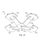
この摩擦素子170の形状は、実質的に円柱型であってよい。他の実施形態では、この摩擦素子170は、多面体形状など他の形状または構成を有する場合もある。この摩擦素子170は、前記圧電素子150に対し、実質的に正方形または長方形の底面を有する場合もある。この摩擦素子170は、前記圧電素子150上に種々の構成で配置された複数の摩擦部材を有する場合もある。例えば、図1bは本開示の態様に従った前記摩擦素子170の異なる別の実施形態に参照番号170aを割り当てたものの斜視図を例示している。前記摩擦素子170aは、圧電素子150(図1a)への取り付け手段(固定穴172など)を有しうる中央部171を含む。支持部材174a〜dはバネ、それ以外の場合は弾性のある部材および/または柔軟な部材であってよく、摩擦部材175a〜dをそれぞれ支持する。前記摩擦部材175a〜d、および可能性として前記摩擦素子170aの要部は、組成および製造上その他、前記摩擦素子170に実質的に類似するものであってもよい(図1a)。
The
図1aに示したように、この摩擦素子170は選択的に摩擦により被駆動素子190に係合する。前記被駆動素子190は、前記ベース110により、1若しくはそれ以上の自由度(移動平面上)で誘導される、または移動を制約される場合がある。例えば前記ベース110は、摩擦滑り素子か、滑り構成を伴った転動体かを使用して、平行移動について所定の自由度または方向、および/または前記被駆動素子190の回転を制約できる。これにより、前記被駆動素子190の運動は1自由度に制限される。ただし、他の実施形態ではより大きい自由度が許される場合もある。前記被駆動素子190は、前記装置100により移動される物体または試験片199を把持または運搬する。例えば、この試験片199は、組み立て中のマイクロコンポーネントまたはナノ装置、または走査型電子顕微鏡(scanning electron microscope、略称SEM)、他の荷電粒子装置、または他タイプの顕微鏡で走査中の試料などであり得る。一部の実施形態では、前記装置100は、前記試験片199を前記被駆動素子190の表面上に掛け留める取り付け手段を含む。例えば、この被駆動素子190は、前記試験片199を受容するように構成された凹部または溝を含む場合があり、あるいはスナップ式または摩擦式の連結部材で前記試験片199を前記被駆動素子190に固定する場合もある。
As shown in FIG. 1a, the
前記被駆動素子190の移動は、前記圧電素子150に電気信号を与えて前記圧電素子150を伸縮させることにより、もたらすことができる。前記摩擦素子170、または前記圧電素子150自体は、前記電気信号の周波数、振幅、および/または形状に基づき、このような移動の一部または全部を前記被駆動素子190に伝達する。例えば、前記装置150で粗位置決めをもたらすには、前記圧電素子150に対する電圧波形を変化させる。電圧波形の例としては、(これに限定はされないが)方形波、のこぎり波、サイクロイド、放物線波、および/またはこれらの重ね合わせまたは組み合わせなどがある。
The driven
例えば、のこぎり波の電圧波形を使用する実施形態の場合、前記圧電素子150は、バイアスまたは極性に従って伸縮する。波形の勾配が比較的緩やかな位相中は、この位相の大部分の間、前記圧電素子150(または前記摩擦素子170)が前記被駆動素子190に「スティック」する(貼り付く)ため、前記圧電素子の動きの大部分または全部が前記被駆動素子190へ伝わり得る。ただし、波形が比較的急勾配な位相中は、前記圧電素子150の伸縮が対応して急激になり、この急勾配な位相の大部分の間、前記圧電素子150(または前記摩擦素子170)は前記被駆動素子190との静止摩擦力を上回って「スリップ」する(滑る)ため、前記圧電素子190の動きはほとんど、または全く前記被駆動素子190へ伝わらない場合がある。波形の勾配が緩やかな位相に戻ると、前記圧電素子150の伸縮は、再びその動きを前記被駆動素子190に伝達するようになる。このように、前記摩擦素子170は、前記被駆動素子190に対する前記摩擦素子170の速度、加速度、および/または摩擦係数の関数として、選択的におよび摩擦により前記被駆動素子190に係合する。これは、「スリップ−スティック」運動または「スティック−スリップ」運動と呼ばれている。
For example, in an embodiment using a sawtooth voltage waveform, the
波形の周波数は場合により異なり、一部の実施形態では約1Hz〜約1kHzの範囲になる。波形の振幅も場合により異なり、一部の実施形態では約2V〜約500Vの範囲になる。前記スリップ−スティック移動による粗位置決め後は、直流電圧を印加して前記被駆動素子190、ひいてはその上に配置された前記物体または試験片199を微細に位置決めする。この直流電圧は、約10mV〜約1kV範囲に成り得る。
The frequency of the waveform varies from case to case and in some embodiments ranges from about 1 Hz to about 1 kHz. The amplitude of the waveform also varies, and in some embodiments ranges from about 2V to about 500V. After the rough positioning by the slip-stick movement, a DC voltage is applied to finely position the driven
他の実施形態では、周波数、振幅、および直流電圧は場合により異なる。例えば、波形は、前記圧電素子150または可能性として前記試験片199の機械的共鳴の励起を回避または最小化するよう形成される。ただし、例えば何らかの事情により前記被駆動素子190が前記摩擦素子170に連結されてしまった(「スタックした」)場合は、前記被駆動素子190を前記摩擦素子170から開放するため、秩序ある共鳴により前記圧電素子に作用するように、波形を意図的に選択する場合もある。前記圧電素子150の共鳴周波数が未知の場合は、波形の周波数掃引を行うこともある。
In other embodiments, the frequency, amplitude, and DC voltage vary from case to case. For example, a waveform is formed to avoid or minimize excitation of mechanical resonances of the
図1aを参照しつつ図2を参照すると、本開示の態様に従った前記装置100の別の実施形態に参照番号200を割り当てたものの断面図が例示されている。図2の実施形態は、図1aに示した実施形態の前述した特徴を多数有している。ただし、この装置200は付勢素子215も有し、さらにこの付勢素子215に連結されたスペーサー220を含む場合もある。例示した実施形態のとおり、前記付勢素子215は、前記圧電素子150(またはそれに取り付けられた前記摩擦素子170)を前記被駆動素子190に抗して付勢するように構成された板バネまたは他タイプのバネであってよい。ただし、前記付勢素子215は、本開示の範囲内で、非択一的または択一的に他の機械的、電気的、および/または磁気的な付勢手段であってよく、またはこれらを含んでよい。前記付勢素子215の付勢力は、例えばネジ式固定部材225、静電場、磁場、および/または他の手段により、調整自在であってよい。ただし、一部の実施形態では調整を行わないか、調整が不要な場合もある。
Referring to FIG. 2 with reference to FIG. 1a, a cross-sectional view of another embodiment of the
前記装置200は、前記被駆動素子190に連結された、あるいは前記被駆動素子190と前記摩擦素子170との間に介在するウェアプレート295を含む場合もある。このウェアプレート295は、シリコン、サファイア、セラミック、アルミニウムセラミック、またはこれらの合金、および/または他の材料を有する場合があり、前記被駆動素子190に連結または一体化される場合がある。一実施形態では、前記ウェアプレート295は、スクライビング、切断、研磨、および/または他の工程により、可能性として約0.1mm〜約1mm範囲の厚さに形成できる。他の実施形態では、前記ウェアプレート295は、化学気相成長法(CVD)、物理気相成長法(PVD)、プラズマ化学気相成長法(PECVD)、原子層成長法(ALD)、および/または他の工程により、可能性として約0.1μm〜約5μm範囲の厚さに形成できる。
The
前記摩擦素子170により前記ウェアプレート295に抗して印加される力(負荷力など)は、前記圧電阻止150上の前記摩擦素子170の位置、前記摩擦素子が「スリップ」位相または「スティック」位相にある時間長、および/または前記ウェアプレート295に対する前記圧電素子150の角度の関数として変調または調整可能である。前記ウェアプレート295に抗する前記摩擦素子170の力の機械的調整手段も、設ける場合がある(ネジ225など)。前記ウェアプレート295に抗する前記摩擦素子170の力の変調の調整も、1若しくはそれ以上の追加圧電素子を介して行う場合があり、前記追加圧電素子は、例えば前記圧電素子150と前記ベース110との間に載置できる。ただし一部の実施形態では、上記の付勢力と同様、調整を行わないか、調整が不要な場合がある。
The force applied by the
前記スペーサー220は、実質的に半球形状のバイトン素子であってよい。ただし、このスペーサー220は、本開示の範囲内で他の材料および形状を有する場合もある。このスペーサー220は、前記付勢素子215による前記スペーサー220の付勢先となる前記圧電素子150に抗する磨耗および振動を低減し得る。
The
前記装置200は、前記被駆動素子190の位置を検出するセンサ296およびセンサ297のシステムを備えている場合がある。これらのセンサ196、297は、フィードバック機構(図示せず)、あるいは別のシステムまたはサブシステムの一部にも成り得る。前記センサ296、297は、容量性または誘導性の電気センサであってもよい。また、前記センサ296、297は、熱的、光学的、磁気的、および/または他タイプのセンサであってもよい。前記センサ296は、単一のセンサ素子として示しているが、複数の素子またはセンサアレイを有する場合もある。同様に、前記センサ297は複数のセンサ素子を含むものとして示しているが、単一のセンサ素子を有する場合もあり、また図示とは異なる数のセンサ素子を有する場合もある。これらの前記センサ296、297は、前記作動部材190および前記圧電素子150とそれぞれ一体化して、またはこれに埋め込んで形成してもよい。また、前記センサ296、297は、例えば接着剤で取り付けられた別個のコンポーネントであってもよい。前記センサ296、297の位置は、場合により図と異なり、前記装置200の他のコンポーネントに関するフィードバックおよび/または位置の情報を提供する他のセンサ(図示せず)があってもよい。一部の実施形態では、単一のセンサのみ設けられる。電子機器ベースのフィードバックまたはセンサシステムに加えて、機械的システムを使ってもよい。例えば、前記圧電素子150により印加される力は、機械的に増幅でき、前記ウェアプレート295に抗する前記摩擦素子170の負荷力を調整するために使用できる。
The
図2を参照しつつ図3を参照すると、本開示の態様に従った、図2に示した前記装置200の別の実施形態に参照番号300を割り当てたものの断面図が例示されている。上記のいくつかのコンポーネントのほか、前記装置300は、載置部材362、264によりそれぞれ前記ベース110に連結されたレストレイント(移動制約部材)352、354を含む。ただし一実施形態では、これらのレストレイントは前記装置300内に固定され得る。例えば、前記レストレイント352は、前記載置部材が不要になるよう前記摩擦素子170または前記被駆動素子190に連結する場合もある。
Referring to FIG. 3 with reference to FIG. 2, there is illustrated a cross-sectional view of another embodiment of the
前記レストレイント362、364は、前記圧電素子150の運動が実質的に縦方向の伸縮だけに制限されるよう、この圧電素子150の曲げ、回転、または他の面外運動を制限し得る。直線運動用に設計された特定の形状および組成の圧電素子は、一定の周波数および一定の負荷下で曲がる動きを呈することが知られている。前記レストレイント352、354は、前記圧電素子150の少なくとも一部に表面接触し続けることにより、このような曲がりを防ぐ。一実施形態では、前記レストレイント352、354は、ガラス、金属、合金、および/または、マイクロスケールの実施形態の材料に類似する、または類似しない他の材料を有する場合があり、約0.1mm〜約1mm範囲の厚さを有し得る。他の実施形態では、前記レストレイント352およびレストレイント354は、シリコン、サファイア、セラミック、アルミニウムセラミック、これらの合金、および/または他の材料を有する場合があり、約0.1μm〜約5μm範囲の厚さを有し得る。一実施形態では、前記レストレイント352は、前記摩擦素子170の厚さにほぼ等しい厚さを有する。
The
前記レストレイント352、354の長さは、前記圧電素子150の長さの約10%〜約95%範囲になり得る。例えば、前記レストレイント352、354の長さを最大化するとき、前記圧電素子150が付勢されない、非作動配置であり得る配置にある場合、可能性として前記圧電阻止150の前記先端に前記摩擦素子170を取り付けるための十分な空間を残しつつ、実質的に前記圧電素子150の長さに及ぶ。一実施形態では、前記レストレイント352、354の長さは、前記圧電素子150の長さの約40%〜約60%範囲に成り得る。前記レストレイント352、354の長さは、形状、サイズ、組成、電気接続などに関して互いに異なる場合もある。
The length of the
前記レストレイント352、354が導電性の実施形態では、前記載置部材362、364は絶縁体としての役割を果たし、前記圧電素子150および前記ベース110の短絡を防止する。一部の実施形態では、これらのレストレイントは導電性だが絶縁層で覆われ、前記圧電素子150および前記ベース110の短絡を防いでいる。前記圧電素子150も、エラストマー層であって、運動を可能にしつつ前記圧電素子150および他のいかなるコンポーネント(前記ベース110など)との短絡も防ぐエラストマー層で覆われる場合がある。また他の実施形態では、図3より多数または少数のレストレイントおよび載置部材が設けられる。
In the embodiment in which the
図2を参照しつつ図4を参照すると、図2に示した前記マイクロ電子装置200の別の実施形態に参照番号400を割り当てたものの断面図が例示されている。上記のコンポーネントに加え、前記装置400は平衡錘465を含む。この平衡錘465は前記圧電素子150の前記先端151に取り付けられる。他の実施形態では、前記平衡錘465の配置は場合により異なり、前記圧電素子150の種々の位置に複数の平衡錘が配置される場合もある。
Referring to FIG. 4 with reference to FIG. 2, there is illustrated a cross-sectional view of another embodiment of the
この平衡錘465は、ステンレス鋼、鉛、および/または他の材料を有してよく、重量は前記圧電素子150の重量の約50%〜約150%範囲である。この平衡錘465は、鋳造、機械加工、電解加工(ECM)、放電加工(EDM)、フライス加工、および/または他の方法で製造できる。前記平衡錘は、前記圧電素子150と一体型にしても、接着剤、固定部材、および/または他の手段で前記圧電素子150に取り付けてもよい。前記平衡錘465の1若しくはそれ以上の横方向寸法は、前記圧電素子150の長さの約10%〜約20%範囲になり得る。前記平衡錘465とその態様とに関し挙げる例は、例示的なものであり、他の実施形態は異なる特性を有す場合もある。
The
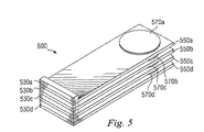
図5は、本開示の態様に従った圧電素子500の一実施形態の斜視図を例示したものである。この圧電素子500は、図1〜図4に示した前記圧電素子150の実施形態の態様の一部を具体化したは、これら圧電部材550a〜dにそれぞれ印加される実質的に類似した電気信号が各前記部材で実質的に類似した伸縮運動を生じるよう、互いに実質的に類似し得る。これらの圧電部材550a〜dは、これらをベースまたは基板(図示せず)に連結する部材としても機能する絶縁体530a〜dにより共通端で結合できる。他の実施形態では、これらの圧電部材をクランプ、接着剤、または積層により互いに一体化する場合もある。これらの圧電部材550a〜dは、摩擦素子570a〜dを介し、調和して運動を被駆動素子に伝達することができ、各前記摩擦素子570a〜dは、組成および製造上、図1aに示した前記摩擦素子170に実質的に類似したものであってよい。
FIG. 5 illustrates a perspective view of one embodiment of a
図6では、図5に示した前記圧電素子500のさらに異なる実施形態に参照番号600を割り当てたものの斜視図を例示している。この圧電素子600は、それぞれ図5に示した前記圧電部材550a〜dに実質的に類似し得る複数の圧電部材650a〜dを有するが、他の構成は本開示の範囲内である。スペーサー630a〜cが介在し、前記圧電部材650a〜dを連結する場合もある。これらスペーサー630a〜0cのうち、前記圧電部材650a〜dの反対端近傍に位置するものもある。例えば例示した実施形態では、前記スペーサー630aは、前記圧電部材650bの前記スペーサー630bに対する反対側(反対面)の反対端近傍にある。
FIG. 6 illustrates a perspective view of a further different embodiment of the
各圧電部材650a〜dは、それぞれ隣り合う圧電部材と反対方向へ付勢され得る。例えば、前記圧電部材650aおよび650cは、前記圧電部材650bおよび650dを伸長させ得る電気信号に応答して収縮し得る。摩擦素子670は、前記圧電部材650a〜dのうち最も外側の1若しくはそれ以上の作動端付近に位置付けてよく、例えば図1a〜図4に示した被駆動素子の係合に使用できる。
Each of the
図7は、本開示の態様に従った装置700の一実施形態の斜視図を例示したものである。この装置700は、2つの独立した移動平面または移動方向をもたらし、圧電素子750に取り付けられたベース710を含む。
FIG. 7 illustrates a perspective view of one embodiment of an
このベース710は、組成および製造上、図1aに示した前記ベース110と実質的に類似したものであってよい。一実施形態では、前記ベース110の長さおよび幅は、双方とも約5mm〜約20mm範囲に成り得る。他の実施形態では、このベース110の長さおよび幅が双方約50μm〜約200μm範囲になる場合もある。
The base 710 may be substantially similar in composition and manufacture to the base 110 shown in FIG. 1a. In one embodiment, the length and width of the base 110 can both range from about 5 mm to about 20 mm. In other embodiments, the length and width of this
前記圧電素子750は、全体として角を成す部材として成形され、可能性として連結または一体化して形成された2つ以上のセグメントを含む。この圧電素子750の成す角度は、約45度〜約135度の範囲に成り得る。この圧電素子750は、上記の圧電素子に類似した材料を有してよく、類似原理に従って製造してよい。一実施形態では、前記圧電素子750の長さおよび幅は、約0.5cm〜約15cm範囲に成り得る。他の実施形態では、この圧電素子750の長さおよび幅は、約50μm〜約200μm範囲になる場合もある。
The
前記装置700は、前記圧電素子750の2つ以上のセグメントの頂点または接合部の付近に取り付けられた摩擦素子770を含む場合もある。この摩擦素子770は、組成および製造上、図1aに示した前記摩擦素子170と実質的に類似したものであってよい。
The
この装置700は、2つの被駆動素子790aおよび790bも含む。前記被駆動素子790aは、前記ベース710に対し第1の方向705へスライドするように構成されており、前記被駆動素子790bは、前記被駆動素子790a(従って前記ベース710)に対し第2の方向707へスライドするように構成されている。一実施形態では、前記第1の方向705および第2の方向707は、実質的に直交し合うが、他の相対配向も本開示の範囲内である。
The
前記圧電素子750は、それぞれ前記摩擦素子770の取り付け点から遠位にある2端で前記ベース710に取り付けてよい。これにより、前記圧電素子750に電気信号を与えて、少なくとも2つの移動平面または移動方向に沿って前記圧電素子750を作動させることが可能になる。この2つの移動方向は、上記のように前記被駆動素子790bの表面を2次元移動するように構成された、2つの別個の部材である前記被駆動素子790a、790bの移動に対応し得る。これらの被駆動素子790a、790bは、それぞれ組成および製造上、図1aに示した前記被駆動素子190と実質的に類似したものであってよい。粗位置決めは、例えば変動する電気信号を適用して、前記被駆動素子790a、790bの一方または双方のスリップ−スティック移動を生ずることにより、もたらすことができる。微細な位置決めは、例えば非変動電気信号を前記圧電素子750に適用することによりもたらすことができる。
The
図8は、本開示の態様に従った装置800の一実施形態の破断図を例示したものである。この装置800は、被駆動素子890に回転運動を生じるように構成できる。この装置800は、ベース810および絶縁体830を含み、前記絶縁体830は、圧電素子850を前記ベース810に取り付けている。前記ベース810と、前記絶縁体830と、前記圧電素子850との組成および製造は、上記の実施形態のものに類似したものであってよい。前記圧電素子850は、スライド自在に摩擦により前記被駆動素子890に係合する摩擦素子870が取り付けられている場合がある。この被駆動素子890は、組成および製造上、図1aに示した前記被駆動素子190に実質的に類似したものであってよく、実質的に円盤形状で、可能性として約0.5cm〜約15cm範囲の直径を有してよい。他の実施形態では、この被駆動素子890の直径は約50μm〜約200μm範囲になり得る。
FIG. 8 illustrates a cutaway view of one embodiment of an
この被駆動素子890は、回転自在に前記ベース810に取り付けてよい。前記被駆動素子890の回転は、第1の変動電気信号を前記圧電素子850に適用することにより、もたらすことができる。変動する電気信号は、前記被駆動素子890のスリップ−スティック移動を生じ得る。スリップ−スティック移動を使うと粗位置決めを実現でき、他方、微細な位置決めは、非変動の電気信号の適用により可能となる。前記被駆動素子890は、前記第1の変動電気信号と異なる形態の変動電気信号を適用すると、反対方向に回転させることができる。
The driven
図9は、本開示の態様に従った装置900の一実施形態の斜視図を例示したものである。この装置900は、被駆動素子990a、990bの回転移動を生じることができ、前述の装置800に類似している。この装置900は、ベース910と、圧電素子950a、950bの取り付け用ブラケット912とを有する。前記ブラケット912は、酸化アルミニウム、セラミック、ベリリウム、真ちゅう、金、および/または他の材料を有し得る。例示した実施形態では、圧電素子950a、950bにそれぞれ電気信号を与えるため、電極955a、955bを採用している。この構成では、前記圧電素子950a、950bに、それぞれ摩擦素子970a、970bを取り付けてよい。これら摩擦素子970a、970bは、被駆動素子990aまたは990b、もしくはその双方に独立に係合し得る(これら摩擦素子970aおよび/または970bは、前記圧電素子950aおよび/または950bの各反対面上に配置できる)。図9の実施形態において、前記装置900は、2つの圧電素子950a、950bと、2つの被駆動素子990a、990bとを含むが、本開示の範囲内で、任意数の圧電素子により係合される任意数の被駆動素子を含んでよい。
FIG. 9 illustrates a perspective view of one embodiment of an
前記被駆動素子990a、990bは、同軸回転するよう中心軸に沿って取り付けられている。これらの被駆動素子990a、990bは、固定ユニットとして回転するように、または互いに独立して回転するするように構成できる。前記被駆動素子990a、990bの粗い回転運動は、前記電極955a、955bを介して前記圧電素子950a、950bに変動電気信号を適用する結果生じるスリップ−スティック運動により制御可能である。この信号は、一方の圧電素子(圧電素子950aなど)が「スリップ」位相になり、他方の圧電素子(圧電素子950bなど)が「スティック」位相になるように与えられる。前記圧電素子950a、950bの一方または双方に非変動電気信号を与えて微細な位置決めを制御することもできる。
The driven
図10は、本開示の態様に従ったマイクロ電子装置1000の別の実施形態の側面図を例示したものである。この装置1000は、被駆動素子1090、1091に、それぞれ基板1011に対し実質的に直交する運動を生じ得る。この装置1000は、前記基板1011上に、またはその上位に載置されたベース1010を有する。前記ベース1010、1011の材料および製造方法は、前述の実施形態のベースについて説明したものに実質的に類似したものであってよい。前記ベース1010、1011は、接着剤および/または他の手段により取り付けられた別個のコンポーネントであっても、互いに一体化したものであってもよい。
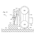
FIG. 10 illustrates a side view of another embodiment of a
付勢素子1015は前記ベース1010に載置され、材料および製造上、上記で説明した付勢素子に対応したものであってよく、場合によってはスペーサー1020が取り付けられており、材料および製造上、上記で説明したスペーサーに対応したものであってよい。前記付勢素子1015の張力は、例えばネジ式固定部材1025および/または他の手段により調整可能である。前記付勢素子1015は、前記圧電素子1050および/またはそれに取り付けられた摩擦素子1070をウェアプレート1095に抗して付勢する。この摩擦素子1070およびウェアプレート1095は、組成および製造上、前述の摩擦素子およびウェアプレートにそれぞれ実質的に類似したものであってよい。一部の実施形態では、前記ウェアプレート1095の有無は任意である。
The
圧電素子1050は、変動電気信号を適用した結果生じるスリップ−スティック運動による粗位置決め用に前記被駆動素子1090を移動するよう作用する。微細な位置決めをもたらすには、非変動電気信号を前記圧電素子1050に適用する。この圧電素子1050は、組成および製造上、上記で説明した圧電素子と実質的に類似したものであってよい。例示した実施形態では、前記被駆動素子1090は、環状のベルト1092を介して前記被駆動素子1091に取り付けられる。前記被駆動素子1090、1091は、組成および製造上、前述の被駆動素子に実質的に類似したものであってよい。ただし、第2の被駆動素子である前記被駆動素子1091は、第1の被駆動素子である前記被駆動素子1090に類似したものであっても、異なったものであってもよい。
The
前記被駆動素子1090、1091を連結する前記ベルト1092は、シリコン、ゴム、ステンレス鋼、および/または他の材料から成るものであってよい。このベルト1092は、長さが約1.5cm〜約45cmの範囲、厚さは約100μm〜約250μmの範囲であり得る。このベルト1092は、実質的に円柱型のローラーまたはテンショナ1093および1094により支持できる。これらのテンショナ1093、1094は、シリコン、金属、および/または他の材料を有してよい。これらのテンショナの寸法は、前記ベルト1092および前記圧電素子1050の寸法に従って設定される。これらのテンショナ1093、1094は、軸受けやポストなどを含む支持構造1099により前記基板1094に回転自在に取り付けることができる。前記ベルト1092は、第1の被駆動素子である前記被駆動素子1090の移動を第2の被駆動素子である前記被駆動素子1091に伝達する。上記で示した寸法は、マクロスケールの実施形態を参照したものであるが、可能性としてマイクロスケールの実施形態を含む、より小さいサイズに前記装置1000をスケーリングすることも可能である。
The
図11は、本開示の態様に従った装置1100の一実施形態の斜視図を例示したものである。この装置1100は、材料、構造、および寸法について、前記装置100(図1a)に実質的に類似したものであってよい。例えば、ベース1110および被駆動素子1190は、材料、構造、および寸法について、前記装置100の前記ベース110および前記被駆動素子190にそれぞれ類似したものであってよい。この装置1100は、両端で前記ベース1110に固定できる圧電素子1150を特徴として備えている。この圧電素子1150は、2つ以上の部分1151、1152を含む部分に区分または分割することもでき、それらの各部は互いに電気的に絶縁できる。絶縁体1130a、1130bは、前記圧電素子1150を前記ベース1110に固定する役割を果たす。これらの絶縁体1130a、1130bは、前記装置100の前記絶縁体130に実質的に類似したものであってよい。前記圧電素子1150は、実質的にリード形状であってよく、それ以外の場合は前記装置100の前記圧電素子150に類似したものであってよい。摩擦素子1170は、実質的中心点で前記圧電素子1150に取り付け可能である。この摩擦素子1170は、前記装置100の前記摩擦素子170に実質的に類似したものであってよい。作動時、前記装置1100は、異なる極性の作動信号を前記圧電素子1150の異なるセクション1151、1152に適用することにより作用する。このような場合、前記圧電素子1150の1セクション(セクション1151)の収縮と、異なる別のセクション(セクション1152)における対応する伸長との結果、前記スライドテーブル1190に抗した前記摩擦素子のスリップ−スティック移動が生じる。
FIG. 11 illustrates a perspective view of one embodiment of an
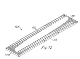
図12は、本開示の態様に従った圧電素子1250用の電極構成1200の一実施形態の斜視図を例示したものである。圧電素子1250は、前記圧電素子150(図1a)など、前述の圧電素子に実質的に類似したものであってよい。主要電極1231は、前記圧電素子1250上に、実質的にその全長にわたり配置される。一部の実施形態では、この主要電極1231は複数の電極である。この主要電極1231の配置は図面と異なる場合もある。この主要電極1231は、銅、金、および/または他の材料を有してよく、これらの材料は前記圧電素子1250上に成膜するか、前記圧電素子1250と一体的に形成し得る。補正電極1232、1233は、前記圧電素子1250上に、実質的にその全長にわたり、可能性として前記主要電極1231の両側辺に配置できる。これらの補正電極1232、1233の数および配置は、場合により図面と異なる。これらの補正電極1232、1233は、銅、金、および/または他の材料を有してよく、これらの材料は前記圧電素子1250上に成膜するか、前記圧電素子1250と一体的に形成し得る。
FIG. 12 illustrates a perspective view of one embodiment of an
前記摩擦素子170(図1a)などの摩擦素子(図示せず)は、前記圧電素子1250に取り付けて被駆動素子(図示せず)の移動を伝達することができる。作動時、前記主要電極1231は、作動信号を前記圧電素子1250に提供するために使用できる。この作動信号は、前述の実施形態に関する説明のとおりであってよい(波形または非変動電圧など)。前記補正電極1232、1233は、前記圧電素子1250の湾曲または移動に補正を加えるため、前記主要電極1231の代わりに、または前記主要電極1231に加えて使用できる。前記主要電極1231と同様、前記補正電極1232、1233からは、前記主要電極1231からの供給電圧より小さい、前記供給電圧より大きい、または前記供給電圧に等しい波形の電圧または非変動電圧を供給してよい。
A friction element (not shown) such as the friction element 170 (FIG. 1a) can be attached to the
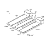
図13は、本開示の態様に従った圧電素子1300の別の実施形態の斜視図を例示したものである。この圧電素子1300は、1若しくはそれ以上の前述の装置(前記装置100など)、または他の装置において利用し得る。この装置1300は、例えば載置部材1330a、1330bにより、ベース(図1aの前記ベース110など)に載置してよい。一部の実施形態では、この載置部材の配置は図示した配置と異なる場合がある。前記圧電素子1300は、材料および構造上、上記で説明した圧電素子に類似したものであってよい。この圧電素子1300は、1若しくはそれ以上の圧電部材1350a〜cを有する場合がある。これらの部材1350a〜cは、一体的に形成しても、別個に形成したのち活着し合ってもよい。電極1331a、1331b、1331cは、前記部材1350a、1350b、1350cとの実質的長さ方向に沿ってそれぞれ取り付けてよい。これらの電極1331a、1331b、電極1331cは、前記電極1231(図12)に実質的に類似したものであってよい。
FIG. 13 illustrates a perspective view of another embodiment of a
作動時、これらの電極1331a〜cは、前記部材1350a〜cにそれぞれ作動信号を適用するため使用できる。前述のとおり、この作動信号は波形の電圧であっても非変動電圧であってもよい。前記電極1331bを介して前記部材1350bに送る信号の極性は、前記電極1331a、1331cを介してそれぞれ前記部材1350a、1350cに送る信号の極性と反対である場合がある。これにより、前記部材1350bの伸長は、前記部材1350a、1350cの収縮に対応し、その逆も言える。摩擦素子1370は、前記圧電素子1300に取り付けてスライドベッド190(図1a)などの被駆動素子(図示せず)と連動させることができる。前記摩擦素子1370は、材料および構造上、前述の摩擦素子(図1aの前記摩擦素子170など)に類似したものであってよい。前記圧電素子1300の熱膨張は、前記摩擦素子1370の望ましくない変位の原因と成り得るが、前記部材1350aと反対方向への前記部材1350bの膨張により回避可能である。
In operation, these
図14は、本開示の装置1400のさらに異なる他の実施形態の斜視図を例示したものである。この装置1400は、材料、構造、および寸法について、前記装置700(図7)に類似したものであってよい。前記装置700同様、この装置1400は、2つの独立な移動平面をもたらし得る(1405および1407など)。この装置1400は、複数の圧電素子1450a〜hを有する場合がある。一部の実施形態では、2つ以上の前記圧電素子1450a〜hを併せる、または角を成した単一の圧電素子750などの(図7)圧電素子として製造することができる。この装置1400は、複数の摩擦素子1470と1471と1472と1473とを有し得る。これら摩擦素子1470と1471と1472と1473とは、摩擦素子770(図7)に実質的に類似したものであってよい。前記圧電素子1450a〜hは、前述の波形に応答して伸縮し、粗位置決め用にスリップ−スティック運動をもたらし得る。微細な位置決めは、前述のとおり前記圧電素子1450a〜hのうち1若しくはそれ以上に非変動電圧の適用によりもたらし得る。
FIG. 14 illustrates a perspective view of yet another alternative embodiment of the apparatus 1400 of the present disclosure. The device 1400 may be similar to the device 700 (FIG. 7) in material, structure, and dimensions. Like the
本開示は、一実施形態において、被駆動素子にスライド自在に係合するように構成されたベースを含む装置を提供する。圧電素子は、前記ベースと前記被駆動素子との間に介在し、前記圧電素子の第1の端近傍で前記ベースに取り付けられている。摩擦素子は、前記圧電素子の第2の端近傍に取り付けられ、選択的に前記被駆動素子に係合するよう構成されている。 The present disclosure, in one embodiment, provides an apparatus that includes a base configured to slidably engage a driven element. The piezoelectric element is interposed between the base and the driven element, and is attached to the base in the vicinity of the first end of the piezoelectric element. The friction element is attached near the second end of the piezoelectric element and is configured to selectively engage the driven element.
また、本開示では、一実施形態において、凹部を有するスライドベッドを含む装置と、内面にウェアプレートを有するスライドテーブルと、摩擦素子が取り付けられた圧電リードとを導入している。前記リードは、前記スライドベッドの前記凹部内に載置され、前記摩擦素子を介して前記ウェアプレートに摩擦により係合する。 Also, in the present disclosure, in one embodiment, an apparatus including a slide bed having a recess, a slide table having a wear plate on the inner surface, and a piezoelectric lead having a friction element attached thereto are introduced. The lead is placed in the recess of the slide bed and engages the wear plate by friction via the friction element.
本開示の態様に従って構成された装置の別の実施形態は、被駆動素子にスライド自在に係合するように構成されたベースと、それぞれ前記ベースに平行な第1および第2の圧電素子とを含む。摩擦素子は、前記第1および第2の圧電素子の接合部近傍にあり、第1の方向および第2の方向に延長する。 Another embodiment of an apparatus configured in accordance with aspects of the present disclosure includes a base configured to slidably engage a driven element, and first and second piezoelectric elements each parallel to the base. Including. The friction element is in the vicinity of the joint between the first and second piezoelectric elements and extends in the first direction and the second direction.
本開示の態様に従った装置の別の実施形態は、回転自在に基板に連結された回転自在な素子を含む。このような実施形態では、圧電素子は前記基板に連結されており、摩擦素子は前記圧電素子に連結されている。この摩擦素子は、前記回転自在な素子に摩擦により係合して、前記回転自在な素子に回転運動を与えるよう構成されている。 Another embodiment of an apparatus according to aspects of the present disclosure includes a rotatable element that is rotatably coupled to a substrate. In such an embodiment, the piezoelectric element is coupled to the substrate and the friction element is coupled to the piezoelectric element. The friction element is configured to be engaged with the rotatable element by friction to give a rotational movement to the rotatable element.
また、本開示の態様に従って構成された装置は、第1および第2の被駆動素子と、前記第1の被駆動素子にスライド自在に係合する圧電素子とを含む場合もある。前記第1および第2の被駆動素子は、少なくとも1つのローラーに支持された連続的で柔軟なベルトを介して互いに連結されている場合がある。 An apparatus configured in accordance with aspects of the present disclosure may also include first and second driven elements and a piezoelectric element slidably engaged with the first driven element. The first and second driven elements may be coupled to each other via a continuous flexible belt supported by at least one roller.
以上、本開示の実施形態を詳述したが、当業者であれば、本開示の要旨を変更しない範囲で種々の変形形態、置換形態、および修正形態が可能であることが理解されることは言うまでもない。 Although the embodiments of the present disclosure have been described in detail above, it is understood by those skilled in the art that various modifications, substitutions, and modifications can be made without departing from the scope of the present disclosure. Needless to say.
本開示は、添付の図面と併せて以下の詳細な説明を読むことにより最もよく理解される。本分野の標準的慣行に基づき、種々の特徴は実際の縮尺どおりに描画されていないことをここに特筆する。例えば、種々の特徴の寸法は、説明を明瞭にするため適宜拡大または縮小している場合がある。
Claims (20)
被駆動素子にスライド自在に係合するように構成されたベースと、
前記ベースと前記被駆動素子との間に介在する圧電素子であって、前記圧電素子の第1の端近傍で前記ベースに取り付けられた圧電素子と、
前記圧電素子の第2の端近傍に取り付けられた摩擦素子であって、前記摩擦素子の前記被駆動素子との相対速度の関数として選択的に前記被駆動素子に係合するように構成された摩擦素子と
を有する装置。 A device,
A base configured to slidably engage a driven element;
A piezoelectric element interposed between the base and the driven element, the piezoelectric element being attached to the base near a first end of the piezoelectric element;
A friction element attached near a second end of the piezoelectric element, wherein the friction element is configured to selectively engage the driven element as a function of a relative speed of the friction element with the driven element. A device having a friction element.
前記被駆動素子に抗して前記圧電素子を付勢するように構成された付勢素子を有するものである。 The apparatus of claim 1, further comprising:
And a biasing element configured to bias the piezoelectric element against the driven element.
前記付勢素子と前記圧電素子との間に介在する振動減衰素子を有するものである。 The apparatus of claim 2, further comprising:
A vibration damping element is interposed between the biasing element and the piezoelectric element.
前記被駆動素子に連結され、選択的に前記摩擦素子に係合されるよう構成されたウェアプレート(耐磨耗板)を有するものである。 The apparatus of claim 1, further comprising:
A wear plate connected to the driven element and selectively engaged with the friction element;
シリコンと、
サファイアと、
セラミックと
からなる群から選択される材料を有するものである。 6. The apparatus of claim 5, wherein the wear plate is
With silicon,
With sapphire,
And having a material selected from the group consisting of ceramics.
前記圧電素子の頂面または底面の少なくとも一方の一部に隣接した低摩擦性のレストレイント(移動制約部材)を有するものである。 The apparatus of claim 1, further comprising:
The piezoelectric element has a low frictional restraint (movement restricting member) adjacent to at least one part of the top surface or the bottom surface of the piezoelectric element.
前記被駆動素子は、前記ベースに連結された実質的に同軸の第1および第2の回転自在部材を含み、
前記圧電素子は、前記ベースに連結された第1および第2の圧電部材を含み、
前記摩擦素子は、前記第1および第2の圧電素子にそれぞれ連結された第1および第2の摩擦部材を含み、
前記第1および第2の摩擦部材は、それぞれ前記第1および第2の回転自在部材に摩擦により係合するものである。 The apparatus of claim 13.
The driven element includes substantially coaxial first and second rotatable members coupled to the base;
The piezoelectric element includes first and second piezoelectric members connected to the base,
The friction element includes first and second friction members coupled to the first and second piezoelectric elements, respectively.
The first and second friction members are engaged with the first and second rotatable members by friction, respectively.
前記ベースは、凹部を有するスライドベッドを含み、
前記被駆動素子は、内面にウェアプレートを有するスライドテーブルを含み、
前記圧電素子は、圧電リードであって、
前記圧電リードは、前記スライドベッドの前記凹部内に載置され、前記摩擦素子を介して前記ウェアプレートに摩擦により係合するものである。 The apparatus of claim 1.
The base includes a slide bed having a recess;
The driven element includes a slide table having a wear plate on the inner surface,
The piezoelectric element is a piezoelectric lead,
The piezoelectric lead is placed in the concave portion of the slide bed, and is engaged with the wear plate by friction via the friction element.
サファイアと、
水晶と、
セラミックと、
アルミニウム青銅と、
リン青銅と、
銅ベリリウムと
からなる群から選択される材料を有するものである。 The apparatus of claim 1, wherein the friction element comprises:
With sapphire,
With crystal,
Ceramic,
Aluminum bronze,
With phosphor bronze,
And having a material selected from the group consisting of copper beryllium.
Applications Claiming Priority (1)
| Application Number | Priority Date | Filing Date | Title |
|---|---|---|---|
| US54635204P | 2004-02-20 | 2004-02-20 |
Publications (1)
| Publication Number | Publication Date |
|---|---|
| JP2005321377A true JP2005321377A (en) | 2005-11-17 |
Family
ID=34826253
Family Applications (1)
| Application Number | Title | Priority Date | Filing Date |
|---|---|---|---|
| JP2005043465A Pending JP2005321377A (en) | 2004-02-20 | 2005-02-21 | Positioning device for microscopic movement |
Country Status (6)
| Country | Link |
|---|---|
| US (1) | US7196454B2 (en) |
| EP (1) | EP1574282A2 (en) |
| JP (1) | JP2005321377A (en) |
| KR (1) | KR20060042979A (en) |
| CN (1) | CN1673067A (en) |
| TW (1) | TW200531420A (en) |
Cited By (3)
| Publication number | Priority date | Publication date | Assignee | Title |
|---|---|---|---|---|
| KR100756224B1 (en) | 2006-06-22 | 2007-09-06 | 전자부품연구원 | Rotary actuating device having means for compensating difference in frictional force |
| JP2016533159A (en) * | 2013-09-13 | 2016-10-20 | フィジック インストゥルメント(ピーアイ)ゲーエムベーハー アンド ツェーオー.カーゲー | Compact general-purpose stick-slip piezoelectric motor |
| JP2017532941A (en) * | 2014-10-09 | 2017-11-02 | アットキューブ システムズ アーゲー | Stick-slip drive, especially piezoelectrically actuated inertial drive |
Families Citing this family (40)
| Publication number | Priority date | Publication date | Assignee | Title |
|---|---|---|---|---|
| US7521932B2 (en) * | 2003-05-06 | 2009-04-21 | The Penn State Research Foundation | Method and system for adjusting the fundamental symmetric mode of coupled high temperature superconductor coils |
| JP2005251745A (en) | 2004-02-23 | 2005-09-15 | Zyvex Corp | Probe operation of charged particle beam device |
| US7326293B2 (en) | 2004-03-26 | 2008-02-05 | Zyvex Labs, Llc | Patterned atomic layer epitaxy |
| TWI237618B (en) * | 2004-06-03 | 2005-08-11 | Ind Tech Res Inst | A long-distance nanometer positioning apparatus |
| EP1828797A1 (en) | 2004-12-03 | 2007-09-05 | E.I. Dupont De Nemours And Company | Decoupling of excitation and receive coils of an nqr detection system during signal reception |
| WO2006135939A2 (en) * | 2005-06-16 | 2006-12-21 | Touchstone Research Laboratory, Ltd. | Microsystem manipulation apparatus |
| US7825567B2 (en) * | 2006-01-20 | 2010-11-02 | Panasonic Corporation | Three-dimensional structure and its manufacturing method |
| WO2007100296A1 (en) * | 2006-03-02 | 2007-09-07 | Nanofactory Instruments Ab | Control signal for inertial slider |
| US8884474B2 (en) * | 2006-06-02 | 2014-11-11 | MicroZeus, LLC | Method of fabricating a micro machine |
| US9156674B2 (en) * | 2006-06-02 | 2015-10-13 | MicroZeus, LLC | Micro transport machine and methods for using same |
| US8159107B2 (en) | 2006-06-02 | 2012-04-17 | Microzeus Llc | Micro rotary machine and methods for using same |
| US8915158B2 (en) * | 2006-06-02 | 2014-12-23 | MicroZeus, LLC | Methods and systems for micro transmissions |
| WO2007143623A2 (en) | 2006-06-02 | 2007-12-13 | Stalford Harold L | Methods and systems for micro machines |
| US8134276B2 (en) * | 2006-06-02 | 2012-03-13 | MicroZeus, LLC | Methods and systems for positioning micro elements |
| US8282284B2 (en) | 2006-06-02 | 2012-10-09 | MicroZeus, LLC | Methods and systems for micro bearings |
| WO2008091371A2 (en) | 2006-07-18 | 2008-07-31 | Multiprobe, Inc. | Apparatus and method for combined micro-scale and nano-scale c-v,q-v, and i-v testing of semiconductor materials |
| US8310128B2 (en) * | 2008-05-07 | 2012-11-13 | The Board Of Trustees Of The University Of Illinois | High precision silicon-on-insulator MEMS parallel kinematic stages |
| US8122973B2 (en) | 2008-05-21 | 2012-02-28 | Stalford Harold L | Three dimensional (3D) robotic micro electro mechanical systems (MEMS) arm and system |
| JP2009296797A (en) * | 2008-06-05 | 2009-12-17 | Olympus Corp | Inertia-driven actuator |
| US20100145511A1 (en) * | 2008-08-18 | 2010-06-10 | Popa Dan O | Microcrawler and conveyor robots, controllers, systems, and methods |
| US8539854B2 (en) * | 2008-10-06 | 2013-09-24 | Board Of Regents, The University Of Texas System | Microrobots with large actuation volumes, and controllers, systems, and methods |
| US8593033B2 (en) * | 2009-06-11 | 2013-11-26 | Micronix Usa | Multi-element, stick-slip piezo motor |
| DE102009057746A1 (en) * | 2009-12-10 | 2011-06-16 | Forschungszentrum Jülich GmbH | nanopositioners |
| WO2012131660A1 (en) * | 2011-04-01 | 2012-10-04 | Ecole Polytechnique Federale De Lausanne (Epfl) | Robotic system for spinal and other surgeries |
| TWI472471B (en) | 2011-06-03 | 2015-02-11 | Academia Sinica | Multi-axes actuating apparatus |
| US8912707B2 (en) * | 2011-07-13 | 2014-12-16 | Academia Sinica | Friction-driven actuator |
| CN102682857B (en) * | 2012-05-14 | 2013-10-16 | 浙江大学 | Device for changing route range of jogged positioning platform |
| US20140380531A1 (en) | 2013-06-24 | 2014-12-25 | Dcg Systems, Inc. | Probe-based data collection system with adaptive mode of probing controlled by local sample properties |
| US9283048B2 (en) | 2013-10-04 | 2016-03-15 | KB Medical SA | Apparatus and systems for precise guidance of surgical tools |
| EP3104803B1 (en) | 2014-02-11 | 2021-09-15 | KB Medical SA | Sterile handle for controlling a robotic surgical system from a sterile field |
| CN106659537B (en) | 2014-04-24 | 2019-06-11 | Kb医疗公司 | The surgical instrument holder used in conjunction with robotic surgical system |
| US10828120B2 (en) | 2014-06-19 | 2020-11-10 | Kb Medical, Sa | Systems and methods for performing minimally invasive surgery |
| JP2017526167A (en) | 2014-06-25 | 2017-09-07 | ディーシージー システムズ、 インコーポレイテッドDcg Systems Inc. | Apparatus and method for nanoprobing of electronic devices |
| US11103316B2 (en) | 2014-12-02 | 2021-08-31 | Globus Medical Inc. | Robot assisted volume removal during surgery |
| US10555782B2 (en) | 2015-02-18 | 2020-02-11 | Globus Medical, Inc. | Systems and methods for performing minimally invasive spinal surgery with a robotic surgical system using a percutaneous technique |
| DE102015208591B4 (en) * | 2015-05-08 | 2016-12-08 | Physik Instrumente (Pi) Gmbh & Co. Kg | Piezoelectric rotary drive with a trained as a leaf spring clamping means |
| EP3344179B1 (en) | 2015-08-31 | 2021-06-30 | KB Medical SA | Robotic surgical systems |
| JP6594175B2 (en) * | 2015-11-20 | 2019-10-23 | キヤノン株式会社 | Vibration wave motor, linear drive device and optical device using the vibration wave motor |
| CN108705329B (en) * | 2018-08-22 | 2023-08-22 | 金陵科技学院 | Precision workbench based on two-degree-of-freedom piezoelectric actuator and corresponding piezoelectric actuator |
| DE102021116325B3 (en) | 2021-06-24 | 2022-09-29 | Physik Instrumente (PI) GmbH & Co KG | Electromechanical drive with a flat stiffening body |
Family Cites Families (82)
| Publication number | Priority date | Publication date | Assignee | Title |
|---|---|---|---|---|
| US3134942A (en) | 1960-12-13 | 1964-05-26 | Richard E Rhodes | Multiple probe resistivity measuring apparatus with workpiece support means |
| US3535515A (en) | 1967-06-14 | 1970-10-20 | Us Navy | Ultrasonic apparatus for electron microscope |
| GB1320346A (en) | 1970-05-22 | 1973-06-13 | Ass Elect Ind | Specimen stages for electron microscopes |
| SE436675B (en) | 1975-08-12 | 1985-01-14 | Ki Politekhnichsky I Im 50 Let | ELECTRIC ENGINE OPERATED BY PIEZOELECTRIC FORCES |
| US4463257A (en) | 1982-08-05 | 1984-07-31 | Tracor Xray Inc. | Rotatable support for selectively aligning a window with the channel of a probe |
| US4587431A (en) | 1983-04-22 | 1986-05-06 | Jeol Ltd. | Specimen manipulating mechanism for charged-particle beam instrument |
| US4601551A (en) | 1984-01-23 | 1986-07-22 | The Micromanipulator Microscope Company, Inc. | Manipulation of embryos and ova |
| JPS61154487A (en) * | 1984-12-26 | 1986-07-14 | Canon Inc | Linear oscillatory wave motor |
| US4736129A (en) * | 1985-05-30 | 1988-04-05 | Marcon Electronics Co., Ltd. | Ultrasonic motor |
| US4678955A (en) | 1986-04-18 | 1987-07-07 | Rca Corporation | Piezoelectric positioning device |
| US4729646A (en) | 1986-05-15 | 1988-03-08 | Bausch & Lomb Incorporated | Multi-use microscope having modular construction of extruded parts |
| US4798989A (en) | 1986-09-26 | 1989-01-17 | Research Development Corporation | Scanning tunneling microscope installed in electron microscope |
| DE3854620T2 (en) | 1987-08-12 | 1996-03-28 | Olympus Optical Co | TUNNEL SCAN MICROSCOPE. |
| DE3879603T2 (en) | 1987-10-09 | 1993-07-01 | Olympus Optical Co | COAXIAL COARSE / FINE ADJUSTER FOR THE OPERATION OF A MICROSCOPE. |
| US5068535A (en) | 1988-03-07 | 1991-11-26 | University Of Houston - University Park | Time-of-flight ion-scattering spectrometer for scattering and recoiling for electron density and structure |
| JPH0272535A (en) | 1988-09-06 | 1990-03-12 | Ube Ind Ltd | Tip sharpening method for electron cathode material |
| US4928030A (en) | 1988-09-30 | 1990-05-22 | Rockwell International Corporation | Piezoelectric actuator |
| US4874979A (en) | 1988-10-03 | 1989-10-17 | Burleigh Instruments, Inc. | Electromechanical translation apparatus |
| FR2639473A1 (en) | 1988-11-18 | 1990-05-25 | Chaixmeca Sarl | DEVICE FOR THE TRANSFER UNDER A CONTROLLED ATMOSPHERE OF SAMPLES FOR EXAMINATION IN TRANSMISSION ELECTRON MICROSCOPY |
| JP2839543B2 (en) | 1989-04-12 | 1998-12-16 | 株式会社東芝 | Displacement generator |
| JP2909829B2 (en) | 1989-07-05 | 1999-06-23 | セイコーインスツルメンツ株式会社 | Compound scanning tunneling microscope with alignment function |
| JPH0687003B2 (en) | 1990-02-09 | 1994-11-02 | 株式会社日立製作所 | Scanning electron microscope with scanning tunneling microscope |
| US5055680A (en) | 1990-04-03 | 1991-10-08 | Lk Technologies, Inc. | Scanning tunneling microscope |
| DE4023311A1 (en) | 1990-07-21 | 1992-01-23 | Omicron Vakuumphysik | ADJUSTMENT DEVICE FOR MICRO MOVEMENTS |
| US5225683A (en) | 1990-11-30 | 1993-07-06 | Jeol Ltd. | Detachable specimen holder for transmission electron microscope |
| US5124645A (en) | 1991-04-24 | 1992-06-23 | The United States Of America As Represented By The Secretary Of The Air Force | Transmission electron microscope (TEM) power probe for in-situ viewing of electromigration and operation of an integrated circuit or microprocessor |
| JP2875066B2 (en) | 1991-07-15 | 1999-03-24 | 日本電子株式会社 | Probe cleaning device for tunnel microscope |
| US5412503A (en) | 1992-08-27 | 1995-05-02 | U.S. Philips Corporation | Specimen holder for a particle beam optical apparatus |
| US5568004A (en) | 1992-09-07 | 1996-10-22 | Kleindiek; Stephan | Electromechanical positioning device |
| JPH0714898A (en) | 1993-06-23 | 1995-01-17 | Mitsubishi Electric Corp | Equipment and method for testing and analyzing semiconductor wafer |
| US5589723A (en) | 1994-03-29 | 1996-12-31 | Minolta Co., Ltd. | Driving apparatus using transducer |
| US5455420A (en) | 1994-07-12 | 1995-10-03 | Topometrix | Scanning probe microscope apparatus for use in a scanning electron |
| US5756997A (en) | 1996-03-04 | 1998-05-26 | General Nanotechnology, L.L.C. | Scanning probe/optical microscope with modular objective/probe and drive/detector units |
| US5989779A (en) | 1994-10-18 | 1999-11-23 | Ebara Corporation | Fabrication method employing and energy beam source |
| US5635836A (en) | 1994-10-21 | 1997-06-03 | International Business Machines Corporation | Mechanical apparatus with rod, pivot, and translation means for positioning a sample for use with a scanning microscope |
| AUPM911194A0 (en) | 1994-10-28 | 1994-11-24 | Biomolecular Research Institute Limited | Sample holder |
| DE9421715U1 (en) | 1994-11-15 | 1996-07-25 | Klocke Volker | Electromechanical positioning unit |
| ATE304737T1 (en) | 1994-12-28 | 2005-09-15 | Univ Delft Tech | SAMPLE HOLDER FOR AN ELECTRON MICROSCOPE AND APPARATUS AND METHOD FOR MOUNTING A SAMPLE IN AN ELECTRON MICROSCOPE |
| DE19524907A1 (en) | 1995-07-08 | 1997-01-09 | Frieder Mugele | Scanning probe microscope - has probe holder, fixed to guide rail, moving macroscopically along rail with all microscope components, including test item but excluding probe holder and the probe, solidly linked together |
| US6000280A (en) | 1995-07-20 | 1999-12-14 | Cornell Research Foundation, Inc. | Drive electrodes for microfabricated torsional cantilevers |
| JPH10104242A (en) | 1996-09-26 | 1998-04-24 | Jeol Ltd | Scanning probe microscope |
| US5922179A (en) | 1996-12-20 | 1999-07-13 | Gatan, Inc. | Apparatus for etching and coating sample specimens for microscopic analysis |
| US5963956A (en) | 1997-02-27 | 1999-10-05 | Telcontar | System and method of optimizing database queries in two or more dimensions |
| JPH10337057A (en) * | 1997-06-02 | 1998-12-18 | Minolta Co Ltd | Driver |
| US6538254B1 (en) | 1997-07-22 | 2003-03-25 | Hitachi, Ltd. | Method and apparatus for sample fabrication |
| JP3900664B2 (en) | 1997-09-26 | 2007-04-04 | 株式会社ニコン | microscope |
| JPH11135015A (en) | 1997-11-04 | 1999-05-21 | Mitsubishi Electric Corp | Manufacture of cathode-ray tube |
| US6002136A (en) | 1998-05-08 | 1999-12-14 | International Business Machines Corporation | Microscope specimen holder and grid arrangement for in-situ and ex-situ repeated analysis |
| JP2000021345A (en) | 1998-07-06 | 2000-01-21 | Hitachi Ltd | Scanning type electron microscope |
| WO2000010191A1 (en) | 1998-08-12 | 2000-02-24 | Gatan, Inc. | Double tilt and rotate specimen holder for a transmission electron microscope |
| US6198299B1 (en) | 1998-08-27 | 2001-03-06 | The Micromanipulator Company, Inc. | High Resolution analytical probe station |
| US6744268B2 (en) | 1998-08-27 | 2004-06-01 | The Micromanipulator Company, Inc. | High resolution analytical probe station |
| DE19940124C2 (en) | 1998-08-31 | 2003-04-10 | Olympus Optical Co | Platform with a displacement enhancement mechanism |
| US6196061B1 (en) | 1998-11-05 | 2001-03-06 | Nanodevices, Inc. | AFM with referenced or differential height measurement |
| US6210988B1 (en) | 1999-01-15 | 2001-04-03 | The Regents Of The University Of California | Polycrystalline silicon germanium films for forming micro-electromechanical systems |
| JP2000260852A (en) | 1999-03-11 | 2000-09-22 | Tokyo Electron Ltd | Inspection stage and device |
| SE515985C2 (en) | 1999-06-13 | 2001-11-05 | Nanofactory Instruments Ab | Device for micropositioning of objects using mechanical inertia |
| DE19935570C2 (en) | 1999-07-30 | 2001-07-05 | Forschungszentrum Juelich Gmbh | Micromanipulator |
| US6583413B1 (en) | 1999-09-01 | 2003-06-24 | Hitachi, Ltd. | Method of inspecting a circuit pattern and inspecting instrument |
| JP2001198896A (en) | 2000-01-19 | 2001-07-24 | Hitachi Ltd | Micro-manipulator for electron microscope |
| US6917845B2 (en) | 2000-03-10 | 2005-07-12 | Smiths Detection-Pasadena, Inc. | Method for monitoring environmental condition using a mathematical model |
| US6870304B2 (en) | 2000-03-23 | 2005-03-22 | Elliptec Resonant Actuator Ag | Vibratory motors and methods of making and using same |
| US6422077B1 (en) | 2000-04-06 | 2002-07-23 | The University Of Chicago | Ultrananocrystalline diamond cantilever wide dynamic range acceleration/vibration/pressure sensor |
| US20020138353A1 (en) | 2000-05-03 | 2002-09-26 | Zvi Schreiber | Method and system for analysis of database records having fields with sets |
| WO2001090761A2 (en) | 2000-05-19 | 2001-11-29 | Imago Scientific Instruments | Methods of sampling specimens for microanalysis |
| WO2002095378A1 (en) | 2000-05-22 | 2002-11-28 | Moore Thomas M | Method for sample separation and lift-out |
| US6539519B1 (en) | 2000-05-31 | 2003-03-25 | Mark D. Meeker | Spatial characteristic and logical hierarchy based manner for compactly storing IC design data and related operations |
| US7292255B2 (en) | 2000-05-31 | 2007-11-06 | Canon Kabushiki Kaisha | Image data acquisition optimisation |
| JP2002033366A (en) | 2000-07-13 | 2002-01-31 | Hitachi Ltd | Probe unit and sample manipulating device using the same |
| US6841788B1 (en) | 2000-08-03 | 2005-01-11 | Ascend Instruments, Inc. | Transmission electron microscope sample preparation |
| AU2001281762A1 (en) | 2000-08-25 | 2002-03-04 | Danmarks Tekniske Universitet | Fabrication and application of nano-manipulators with induced growth |
| US6856712B2 (en) | 2000-11-27 | 2005-02-15 | University Of Washington | Micro-fabricated optical waveguide for use in scanning fiber displays and scanned fiber image acquisition |
| WO2002071031A1 (en) | 2001-03-01 | 2002-09-12 | Moore Thomas M | Total release method for sample extraction from a charged particle instrument |
| US6862921B2 (en) | 2001-03-09 | 2005-03-08 | Veeco Instruments Inc. | Method and apparatus for manipulating a sample |
| JP4200665B2 (en) | 2001-05-08 | 2008-12-24 | 株式会社日立製作所 | Processing equipment |
| JP4229837B2 (en) | 2001-09-24 | 2009-02-25 | エフ イー アイ カンパニ | Electrostatic manipulating device |
| KR20040048933A (en) | 2001-10-04 | 2004-06-10 | 코닌클리케 필립스 일렉트로닉스 엔.브이. | Method of styling a user interface and device with adaptive user interface |
| JP3820964B2 (en) | 2001-11-13 | 2006-09-13 | 株式会社日立製作所 | Sample observation apparatus and method using electron beam |
| US6671710B2 (en) | 2002-05-10 | 2003-12-30 | Energy Conversion Devices, Inc. | Methods of computing with digital multistate phase change materials |
| US6891170B1 (en) | 2002-06-17 | 2005-05-10 | Zyvex Corporation | Modular manipulation system for manipulating a sample under study with a microscope |
| US6995380B2 (en) | 2003-03-13 | 2006-02-07 | Ascend Instruments, Llc | End effector for supporting a microsample |
| JP2005251745A (en) | 2004-02-23 | 2005-09-15 | Zyvex Corp | Probe operation of charged particle beam device |
-
2005
- 2005-02-05 TW TW094104097A patent/TW200531420A/en unknown
- 2005-02-14 EP EP05250832A patent/EP1574282A2/en not_active Withdrawn
- 2005-02-18 CN CNA2005100093933A patent/CN1673067A/en active Pending
- 2005-02-18 US US11/061,076 patent/US7196454B2/en active Active
- 2005-02-18 KR KR1020050013496A patent/KR20060042979A/en not_active Application Discontinuation
- 2005-02-21 JP JP2005043465A patent/JP2005321377A/en active Pending
Cited By (3)
| Publication number | Priority date | Publication date | Assignee | Title |
|---|---|---|---|---|
| KR100756224B1 (en) | 2006-06-22 | 2007-09-06 | 전자부품연구원 | Rotary actuating device having means for compensating difference in frictional force |
| JP2016533159A (en) * | 2013-09-13 | 2016-10-20 | フィジック インストゥルメント(ピーアイ)ゲーエムベーハー アンド ツェーオー.カーゲー | Compact general-purpose stick-slip piezoelectric motor |
| JP2017532941A (en) * | 2014-10-09 | 2017-11-02 | アットキューブ システムズ アーゲー | Stick-slip drive, especially piezoelectrically actuated inertial drive |
Also Published As
| Publication number | Publication date |
|---|---|
| US7196454B2 (en) | 2007-03-27 |
| US20050184623A1 (en) | 2005-08-25 |
| EP1574282A2 (en) | 2005-09-14 |
| KR20060042979A (en) | 2006-05-15 |
| TW200531420A (en) | 2005-09-16 |
| CN1673067A (en) | 2005-09-28 |
Similar Documents
| Publication | Publication Date | Title |
|---|---|---|
| JP2005321377A (en) | Positioning device for microscopic movement | |
| US9018823B2 (en) | Apparatus and method for electromechanical positioning | |
| EP1672654B1 (en) | Microelectromechanical System Actuator | |
| US6604295B2 (en) | Microscopic geometry measuring device | |
| US7372025B2 (en) | Scanning probe microscope using a surface drive actuator to position the scanning tip | |
| JPH04122806A (en) | Micromotion scanning mechanism of interatomic force microscope | |
| WO2015113998A1 (en) | Positioning motor and method of operation | |
| US9385635B2 (en) | Ultrasonic motor | |
| JPH0744857B2 (en) | Piezoelectric rotating device | |
| US20160336504A1 (en) | Positioning Device | |
| US20090212657A1 (en) | Equivalent-capacitance type actuator drive device | |
| JP3844114B2 (en) | Endless orbit translation rotation stage | |
| JP2002184339A (en) | Breaking mechanism and sample stage for electron microscope | |
| JP4074218B2 (en) | Moving stage device and scanning probe microscope | |
| Müller et al. | Piezo-based, long-travel actuators for special environmental conditions | |
| WO2003061107A2 (en) | Dielectric actuator including conductive gap | |
| US20230387828A1 (en) | Piezoelectric motors with nanometer-level resolution | |
| JP2005102368A (en) | Driving device | |
| CN112466594B (en) | Electric control vector magnetic field device and installation method thereof | |
| JP2005010058A (en) | Moving stage device and scanning probe microscope | |
| KR20060085044A (en) | Discrete microactuator and method of operation thereof | |
| JPS6235919A (en) | Portable stage | |
| WO2024035597A2 (en) | Nanopositioner and piezoelectric actuator | |
| JP4554054B2 (en) | Piezoelectric actuator | |
| JP5457593B1 (en) | Drive device |