JP2005311368A - Magnetic random access memory and method of manufacturing same - Google Patents
Magnetic random access memory and method of manufacturing same Download PDFInfo
- Publication number
- JP2005311368A JP2005311368A JP2005119349A JP2005119349A JP2005311368A JP 2005311368 A JP2005311368 A JP 2005311368A JP 2005119349 A JP2005119349 A JP 2005119349A JP 2005119349 A JP2005119349 A JP 2005119349A JP 2005311368 A JP2005311368 A JP 2005311368A
- Authority
- JP
- Japan
- Prior art keywords
- write line
- magnetic
- width
- random access
- access memory
- Prior art date
- Legal status (The legal status is an assumption and is not a legal conclusion. Google has not performed a legal analysis and makes no representation as to the accuracy of the status listed.)
- Pending
Links
- 230000005291 magnetic effect Effects 0.000 title claims abstract description 67
- 238000004519 manufacturing process Methods 0.000 title abstract description 8
- 239000010410 layer Substances 0.000 claims description 49
- 239000000463 material Substances 0.000 claims description 26
- 238000000034 method Methods 0.000 claims description 13
- 239000000758 substrate Substances 0.000 claims description 5
- 239000000126 substance Substances 0.000 claims description 4
- 238000005253 cladding Methods 0.000 claims description 3
- 230000005294 ferromagnetic effect Effects 0.000 claims description 3
- 238000005498 polishing Methods 0.000 claims description 3
- 239000012790 adhesive layer Substances 0.000 claims description 2
- 239000002885 antiferromagnetic material Substances 0.000 claims description 2
- 239000003989 dielectric material Substances 0.000 claims description 2
- PWHULOQIROXLJO-UHFFFAOYSA-N Manganese Chemical compound [Mn] PWHULOQIROXLJO-UHFFFAOYSA-N 0.000 claims 1
- 239000011231 conductive filler Substances 0.000 claims 1
- 229910052748 manganese Inorganic materials 0.000 claims 1
- 239000011572 manganese Substances 0.000 claims 1
- 238000007517 polishing process Methods 0.000 claims 1
- 239000004020 conductor Substances 0.000 description 9
- 239000000696 magnetic material Substances 0.000 description 4
- 230000005669 field effect Effects 0.000 description 3
- 238000002955 isolation Methods 0.000 description 3
- 230000008569 process Effects 0.000 description 3
- 239000010409 thin film Substances 0.000 description 3
- XEEYBQQBJWHFJM-UHFFFAOYSA-N Iron Chemical compound [Fe] XEEYBQQBJWHFJM-UHFFFAOYSA-N 0.000 description 2
- PXHVJJICTQNCMI-UHFFFAOYSA-N Nickel Chemical compound [Ni] PXHVJJICTQNCMI-UHFFFAOYSA-N 0.000 description 2
- 230000004888 barrier function Effects 0.000 description 2
- 238000000151 deposition Methods 0.000 description 2
- 230000004907 flux Effects 0.000 description 2
- 230000006870 function Effects 0.000 description 2
- 239000011148 porous material Substances 0.000 description 2
- RYGMFSIKBFXOCR-UHFFFAOYSA-N Copper Chemical compound [Cu] RYGMFSIKBFXOCR-UHFFFAOYSA-N 0.000 description 1
- XAGFODPZIPBFFR-UHFFFAOYSA-N aluminium Chemical compound [Al] XAGFODPZIPBFFR-UHFFFAOYSA-N 0.000 description 1
- 238000003491 array Methods 0.000 description 1
- 229910017052 cobalt Inorganic materials 0.000 description 1
- 239000010941 cobalt Substances 0.000 description 1
- GUTLYIVDDKVIGB-UHFFFAOYSA-N cobalt atom Chemical compound [Co] GUTLYIVDDKVIGB-UHFFFAOYSA-N 0.000 description 1
- 239000012141 concentrate Substances 0.000 description 1
- 229910052802 copper Inorganic materials 0.000 description 1
- 239000010949 copper Substances 0.000 description 1
- 238000010586 diagram Methods 0.000 description 1
- 238000005530 etching Methods 0.000 description 1
- 229910052742 iron Inorganic materials 0.000 description 1
- WPBNNNQJVZRUHP-UHFFFAOYSA-L manganese(2+);methyl n-[[2-(methoxycarbonylcarbamothioylamino)phenyl]carbamothioyl]carbamate;n-[2-(sulfidocarbothioylamino)ethyl]carbamodithioate Chemical compound [Mn+2].[S-]C(=S)NCCNC([S-])=S.COC(=O)NC(=S)NC1=CC=CC=C1NC(=S)NC(=O)OC WPBNNNQJVZRUHP-UHFFFAOYSA-L 0.000 description 1
- 229910052751 metal Inorganic materials 0.000 description 1
- 239000002184 metal Substances 0.000 description 1
- 238000012986 modification Methods 0.000 description 1
- 230000004048 modification Effects 0.000 description 1
- 229910052759 nickel Inorganic materials 0.000 description 1
- 238000001020 plasma etching Methods 0.000 description 1
- 239000004065 semiconductor Substances 0.000 description 1
Images

Classifications
-
- G—PHYSICS
- G11—INFORMATION STORAGE
- G11C—STATIC STORES
- G11C11/00—Digital stores characterised by the use of particular electric or magnetic storage elements; Storage elements therefor
- G11C11/02—Digital stores characterised by the use of particular electric or magnetic storage elements; Storage elements therefor using magnetic elements
- G11C11/14—Digital stores characterised by the use of particular electric or magnetic storage elements; Storage elements therefor using magnetic elements using thin-film elements
- G11C11/15—Digital stores characterised by the use of particular electric or magnetic storage elements; Storage elements therefor using magnetic elements using thin-film elements using multiple magnetic layers
-
- G—PHYSICS
- G11—INFORMATION STORAGE
- G11C—STATIC STORES
- G11C5/00—Details of stores covered by group G11C11/00
- G11C5/06—Arrangements for interconnecting storage elements electrically, e.g. by wiring
- G11C5/063—Voltage and signal distribution in integrated semi-conductor memory access lines, e.g. word-line, bit-line, cross-over resistance, propagation delay
Landscapes
- Engineering & Computer Science (AREA)
- Computer Hardware Design (AREA)
- Mram Or Spin Memory Techniques (AREA)
- Hall/Mr Elements (AREA)
- Semiconductor Memories (AREA)
Abstract
Description
本発明は、不揮発性メモリに関し、特に磁気ランダムアクセスメモリに関する。 The present invention relates to a nonvolatile memory, and more particularly to a magnetic random access memory.
磁気ランダムアクセスメモリ(Magnetic Random Access Memory:MRAM)は、高速プログラム化を行うことのできる高密度な不揮発性メモリである。MRAMには、複数のメモリセルまたはメモリセルアレイおよび互いに交差された複数のワード線およびビット線が含まれる。従来の磁気メモリセルには、磁気トンネル接合面(Magnet Tunnel Junction:MTJ)、分離トランジスタおよび交差されたワード線およびビット線が含まれる。そして、前述の分離トランジスタは一般にN型電界効果トランジスタ(Field Effect Transistor:FET)であり、互いに接続されたセルにより、分離トランジスタを磁気トンネル接合面、ビット線および一部磁場を発生させてプログラム化されたMRAMセルのワード線にそれぞれ接続する。 Magnetic Random Access Memory (MRAM) is a high-density nonvolatile memory that can be programmed at high speed. The MRAM includes a plurality of memory cells or memory cell arrays and a plurality of word lines and bit lines intersecting each other. A conventional magnetic memory cell includes a magnetic tunnel junction (MTJ), an isolation transistor, and crossed word lines and bit lines. The isolation transistor described above is generally an N-type field effect transistor (FET), and the isolation transistor is programmed by generating a magnetic tunnel junction surface, a bit line, and a partial magnetic field by cells connected to each other. Each of the MRAM cells is connected to a word line.
MTJセルには非磁性導体が主に含まれ、下方の電性接点、プラグ式磁性層、プラグ式磁性層上に設けられたトンネルバリア層、トンネルバリア層上に設けられた自由磁性層(Free Magnetic Layer)が形成され、その自由磁性層上には上方の接点が設けられている。 The MTJ cell mainly includes a nonmagnetic conductor, and includes a lower electrical contact, a plug-type magnetic layer, a tunnel barrier layer provided on the plug-type magnetic layer, and a free magnetic layer provided on the tunnel barrier layer (Free Magnetic Layer) is formed, and an upper contact point is provided on the free magnetic layer.
プラグ式磁性層は、永久に同じ方向を向いている磁気ベクトルを有し、自由磁性層の磁気ベクトルは固定されていないが、当該層の物理サイズにより制限されて二つの方向のうちの一方向を向いている。MTJセルは回路中で接続のために使用される。そして、このMTJセルを介してその内の一層からもう一つの層へ電流を垂直に流す。MTJセルは電性が対応した抵抗でもよく、その抵抗値の大きさは磁気ベクトルの方向により決められる。当該技術に習熟した者なら分かるように、それら磁気ベクトルの指向が反対方向のときは、MTJセルの抵抗値は高くなり、磁気ベクトルの指向が同じ方向のときは、MTJセルの抵抗値は低くなる。 A plug-type magnetic layer has a magnetic vector that is permanently oriented in the same direction and the magnetic vector of the free magnetic layer is not fixed, but is limited by the physical size of the layer and is one of the two directions Facing. MTJ cells are used for connection in the circuit. Then, a current is vertically passed from one of the layers to the other through the MTJ cell. The MTJ cell may be a resistance corresponding to electrical properties, and the magnitude of the resistance value is determined by the direction of the magnetic vector. As those skilled in the art know, when the direction of the magnetic vector is in the opposite direction, the resistance value of the MTJ cell is high, and when the direction of the magnetic vector is in the same direction, the resistance value of the MTJ cell is low. Become.
基本的にビット線はMTJセルアレイの各行と関係し、ワード線はMTJセルアレイの各列と関係する。ビット線およびワード線は、アレイ中のそれぞれのセルアドレスへ用いられ、読み取りやプログラム化を行ったりデータをアレイ中へ保存したりする。また、所定の電流を所定のセルのビット線およびワード線へ印加することにより、所定のセルに対してプログラム化を行うことができる。本実施形態において、書き込み電流(written current)が発生させる磁場は改変データ層(または自由磁性層)の方向へ使用されるため、書き込み電流が印加されるとデータは直ちに書き込まれる。 Basically, a bit line is associated with each row of the MTJ cell array, and a word line is associated with each column of the MTJ cell array. Bit lines and word lines are used for each cell address in the array to read or program and store data in the array. Further, by applying a predetermined current to a bit line and a word line of a predetermined cell, it is possible to program the predetermined cell. In the present embodiment, since the magnetic field generated by the written current is used in the direction of the modified data layer (or free magnetic layer), data is immediately written when the write current is applied.
理論上、低抵抗値(平行ベクトル)の状態では抵抗値が極力小さくなり、高抵抗値(反平行ベクトル)の状態では抵抗値が極力大きくなるため、その変化は関連電子回路においてとても容易に検知することができる。そのため、従来技術では改良された高密度のMRAM素子が求められていた。 Theoretically, the resistance value is as small as possible in the low resistance (parallel vector) state, and the resistance value is as large as possible in the high resistance (antiparallel vector) state. can do. Therefore, an improved high density MRAM device has been demanded in the prior art.
本発明の目的は、高密度のMRAMおよびその製造方法を提供することにある。 An object of the present invention is to provide a high-density MRAM and a manufacturing method thereof.
上述の目的を達成するため、本発明は、MRAMおよびその製造方法を提供する。本発明のMRAMは、磁気トンネル接合面、第1の書き込み線および第2の書き込み線を備える。第2の書き込み線は、第1の書き込み線と直角に交わり、第1の書き込み線および第2の書き込み線のうちの少なくとも一つは、その幅が磁気トンネル接合面の幅よりも小さい。 In order to achieve the above object, the present invention provides an MRAM and a manufacturing method thereof. The MRAM of the present invention includes a magnetic tunnel junction surface, a first write line, and a second write line. The second write line intersects the first write line at a right angle, and at least one of the first write line and the second write line has a width smaller than the width of the magnetic tunnel junction surface.
本発明は書き込み線の幅がMTJセルの幅よりも小さいため、MRAMが使用する面積を効果的に縮小することができる。また、取り囲む磁性材料またはキーパー層を使用することによりMRAMのメモリアレイの磁場を増大させることができる。また、この改良された製造方法により、書き込み線の平坦でないCMP表面が素子不良を発生させる可能性を低減させることができる。 In the present invention, since the width of the write line is smaller than the width of the MTJ cell, the area used by the MRAM can be effectively reduced. Also, the magnetic field of the MRAM memory array can be increased by using a surrounding magnetic material or keeper layer. In addition, this improved manufacturing method can reduce the possibility that a non-flat CMP surface of the write line will cause a device failure.
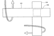
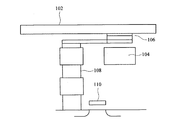
図1Aは、従来のMRAMセルの構造を示す平面図であり、図1Bは、従来のMRAMセルの構造を示す側面図である。書き込み線102はもう一つの書き込み線104の上方に設けられ、この書き込み線104は、磁気トンネル接合面(MTJ)セル106により書き込み線102と分離されて直角に交わる。磁気トンネル接合面106は、さらに連結セル108によりN型電界効果トランジスタ(FET)110に接続される。この従来技術では、均一な磁場によりMTJセル106へ書き込むため、書き込み線102、104の幅が、図示するようにMTJセル106の幅よりも大きくなっており、書き込み操作を行うときに磁場電流を適当に変換することができた。
FIG. 1A is a plan view showing the structure of a conventional MRAM cell, and FIG. 1B is a side view showing the structure of a conventional MRAM cell. The
しかし、書き込み線の幅の大きさは、セルの密度に反比例して、書き込み電流の大きさに正比例するため、MRAMの設計には非常にコストがかかった。その他、書き込み電流密度の減少もまた磁束効率を悪化させ、MRAMの機能をさらに低下させた。 However, since the width of the write line is inversely proportional to the cell density and directly proportional to the write current, the MRAM design is very expensive. In addition, a decrease in write current density also deteriorated the magnetic flux efficiency and further reduced the function of the MRAM.
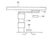
図2Aは、本発明の好適な一実施形態によるMRAMセルの構造を示す平面図であり、図2Bは、本発明の好適な一実施形態によるMRAMセルの構造を示す側面図である。書き込み線202は、もう一つの書き込み線204の上方に設けられ、この書き込み線204は、磁気トンネル接合面(MTJ)セル106により書き込み線202と分離されて直角に交わる。磁気トンネル接合面106は、さらに連結セル206によりN型電界効果トランジスタ(FET)208に接続される。
FIG. 2A is a plan view illustrating a structure of an MRAM cell according to a preferred embodiment of the present invention, and FIG. 2B is a side view illustrating a structure of an MRAM cell according to a preferred embodiment of the present invention. The
本実施形態の書き込み線202、204の幅は、MTJセル106の幅よりも小さい。ここで注意しなければならないこととしては、MTJの形状が矩形や正方形であっても、ここで述べる幅とは任意の一辺の長さを示しているということがある。従来のMRAMセルと異なり、本実施形態は少なくとも一つの書き込み線の幅をMTJセルの一辺よりも小さくするだけで、セルの密度を高めて、特定の書き込み線の電流を低減することができる。また、均一でない磁場が印加されても、MRAMセルの切換の臨界電流は増大しない。その書き込み線は、その当時の技術における最小デザインルール(minimum design rule)と同様に狭く設計される可能性がある。しかし、その線幅が狭すぎる場合、不均一な磁場を発生させて書き込みエラーが起きることがあった。そのため、本実施形態による書き込み線の幅は、MTJセルの幅の半分よりも大きく設定している。他の実施形態では、書き込み線の幅の長さをMTJセルの幅の半分からMTJセルと同じ幅の間に設定してもよい。
The width of the
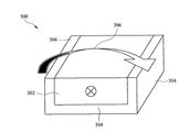
図3は、本発明の好適な一実施形態によるMRAMセルの第1の改良構造を示す斜視図である。図3は、書き込み線の断面構造300を示す斜視図であり、この断面構造は導電材料302を含み、それは強磁性クラッド層および反強磁性材料層を含むシールド層304と結合されている。導電材料302は銅またはアルミニウム金属であり、強磁性クラッド層は鉄、コバルト、マンガン、ニッケルなどの材料からなる。シールド層304は、キーパー層(Keeper Layer)として作用し、MTJセルで見られる磁場306を集中または強化する。また、本実施形態では、酸化物エッチング法、材料堆積法および化学機械的研磨法を含む従来の半導体製造工程によりシールド層304を形成することができる。当該技術に習熟している者なら分かるように、磁性材料のシールド層304は、電流が書き込み線を流れたときの磁束効率を向上させることができる。そのため、書き込み線の幅をさらに小さくすることができるだけでなく、書き込み電流をより少なくすることもできる。
FIG. 3 is a perspective view showing a first improved structure of an MRAM cell according to a preferred embodiment of the present invention. FIG. 3 is a perspective view illustrating a
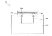
図4は、従来技術の書き込み線の上方に形成される磁気トンネル接合面を示す模式図である。具体的に説明すると、従来技術においては化学機械的研磨法(Chemical Mechanical Polishing:CMP)によりMRAMセルの下層導電線が形成される。図4の断面構造400はMTJセル構造のパターンおよび書き込み線を示し、この断面構造400には酸化物402、導体404およびMTJセル406が含まれる。そして、CMP工程が完了すると、導体404と酸化物402との除去率の差異により、図4の二つの点線円408に示されるように、導体線の上方辺縁にポアがよく形成された。
FIG. 4 is a schematic diagram showing a magnetic tunnel junction surface formed above a conventional write line. More specifically, in the prior art, lower conductive lines of the MRAM cell are formed by chemical mechanical polishing (CMP). The
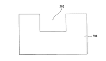
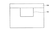
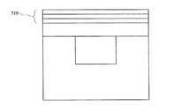
上述の問題を解決するため、図5Aから図5DのMRAMセルの構造に示すように、本発明の好適な一実施形態は改善された工程ステップを提供する。図5Aに示すように、マスクおよびプラズマエッチング技術により、誘電材料の基板504上にトレンチ502を形成する。続いて、図5Bに示すように、充填材料506をトレンチ502中に充填し、トレンチの開口を被覆して書き込み線を形成する。
To solve the above problems, a preferred embodiment of the present invention provides improved process steps, as shown in the structure of the MRAM cell of FIGS. 5A-5D. As shown in FIG. 5A, a
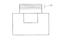
充填材料506は、例えば金属などの導体材料である。書き込み線に磁性を有するキーパー層を設ける場合には、充填材料を充填する前にトレンチ中へ磁性材料を入れる。また、キーパー層と充填材料との間に粘着層を形成して、キーパー層と充填材料との間の接続性を高めてもよい。その後、材料層508を堆積してトレンチ502を被覆する。材料層508を堆積する前には、先ずトレンチ中の導電材料の表面および基板の表面を平坦化する。ここで注意しなければならないこととして、トレンチ502内の導電の書き込み線と材料層508とを電性接続することができるなら、他の構造設計および製造工程を使用してもよく、充填材料506の材料と材料層508の材料とは必ずしも同じでなくともよいということがある。この工程では、一つの材料に対してCMP工程が行われるため、材料層508の表面領域をより平坦化することができる。その後、図5Cに示すように、複数の材料薄膜510を堆積してMTJセル構造を形成する。最後に図5Dに示すように、材料層508の一部および複数の薄膜510の一部を除去してMTJセル512を形成する。
The filling
材料層508を書き込み線506とMTJセル512との間に設けてバッファ層(Buffer Layer)にすることにより、書き込み線506との完全な電性接触を行うとともに、MTJセル512との平坦な接触表面を得ることができる。このように、CMP工程は均一な処理を行うことができ、CMP工程により機能に影響を与えるポアが形成されないようにすることができる。
A
そして、書き込み線の幅がMTJセルの幅よりも小さいために、MRAMメモリが使用する面積を効果的に小さくすることができる。本実施形態は取り囲む磁性材料またはキーパー層を使用してMRAMメモリアレイの磁場を増加させることができる。また、この改良された製造方法により、書き込み線の平坦でないCMP表面により素子不良を発生させる可能性を低減させることができる。 Since the width of the write line is smaller than the width of the MTJ cell, the area used by the MRAM memory can be effectively reduced. This embodiment can use the surrounding magnetic material or keeper layer to increase the magnetic field of the MRAM memory array. In addition, this improved manufacturing method can reduce the possibility of device failure due to the uneven CMP surface of the write line.
本発明では好適な実施形態を前述の通り開示したが、これらは決して本発明を限定するものではなく、当該技術に熟知するものなら誰でも、本発明の主旨と領域を脱しない範囲内で各種の変更や修正を加えることができる。従って、本発明の保護の範囲は、特許請求の範囲で指定した内容を基準とする。 The preferred embodiments of the present invention have been disclosed as described above, but these are not intended to limit the present invention in any way, and anyone who is familiar with the technology can use various embodiments within the scope and spirit of the present invention. Changes and modifications can be made. Therefore, the scope of protection of the present invention is based on the contents specified in the claims.
106 磁気トンネル接合面、202、204 書き込み線、206、208 連結セル、300 断面構造、302 導電材料、304 シールド層、306 磁場、502 トレンチ、504 基板、506 充填材料、508 材料層、510 薄膜、512 MTJセル 106 Magnetic tunnel interface, 202, 204 Write line, 206, 208 Connection cell, 300 Cross-sectional structure, 302 Conductive material, 304 Shield layer, 306 Magnetic field, 502 Trench, 504 Substrate, 506 Filling material, 508 Material layer, 510 Thin film, 512 MTJ cell
Claims (13)
前記第2の書き込み線は、前記第1の書き込み線と直角に交わり、前記第1の書き込み線または前記第2の書き込み線のうちの少なくとも一つは、その幅が前記磁気トンネル接合面の幅よりも小さいことを特徴とする磁気ランダムアクセスメモリ。 Comprising a magnetic tunnel junction surface, a first write line and a second write line;
The second write line intersects the first write line at a right angle, and at least one of the first write line or the second write line has a width that is the width of the magnetic tunnel junction surface. Magnetic random access memory characterized by being smaller than.
前記トレンチに導電充填材料を充填する工程と、
前記導電充填材料上に導電バッファ層を形成する工程と、
前記導電バッファ層に接触される磁気トンネル接合面を形成する工程と、
を少なくとも含むことを特徴とする磁気ランダムアクセスメモリの書き込み線の形成方法。 Forming a trench in the substrate;
Filling the trench with a conductive filler material;
Forming a conductive buffer layer on the conductive filling material;
Forming a magnetic tunnel junction surface in contact with the conductive buffer layer;
A method for forming a write line of a magnetic random access memory, comprising:
13. The method for forming a write line of a magnetic random access memory according to claim 12, further comprising a step of forming an adhesive layer between the conductive filling material and the magnetic layer.
Applications Claiming Priority (1)
| Application Number | Priority Date | Filing Date | Title |
|---|---|---|---|
| US10/827,769 US7105879B2 (en) | 2004-04-20 | 2004-04-20 | Write line design in MRAM |
Publications (1)
| Publication Number | Publication Date |
|---|---|
| JP2005311368A true JP2005311368A (en) | 2005-11-04 |
Family
ID=35097360
Family Applications (1)
| Application Number | Title | Priority Date | Filing Date |
|---|---|---|---|
| JP2005119349A Pending JP2005311368A (en) | 2004-04-20 | 2005-04-18 | Magnetic random access memory and method of manufacturing same |
Country Status (4)
| Country | Link |
|---|---|
| US (2) | US7105879B2 (en) |
| JP (1) | JP2005311368A (en) |
| CN (1) | CN100454433C (en) |
| TW (1) | TWI267977B (en) |
Families Citing this family (5)
| Publication number | Priority date | Publication date | Assignee | Title |
|---|---|---|---|---|
| KR100615089B1 (en) * | 2004-07-14 | 2006-08-23 | 삼성전자주식회사 | Magnetic ram with low drive current |
| US7372722B2 (en) * | 2003-09-29 | 2008-05-13 | Samsung Electronics Co., Ltd. | Methods of operating magnetic random access memory devices including heat-generating structures |
| US7369428B2 (en) * | 2003-09-29 | 2008-05-06 | Samsung Electronics Co., Ltd. | Methods of operating a magnetic random access memory device and related devices and structures |
| US7217666B2 (en) * | 2004-03-02 | 2007-05-15 | Hitachi Global Storage Technologies Netherlands B.V. | Reactive ion milling/RIE assisted CMP |
| US7543211B2 (en) * | 2005-01-31 | 2009-06-02 | Everspin Technologies, Inc. | Toggle memory burst |
Citations (5)
| Publication number | Priority date | Publication date | Assignee | Title |
|---|---|---|---|---|
| JP2002118239A (en) * | 2000-07-21 | 2002-04-19 | Hewlett Packard Co <Hp> | Optimum write conductor layout for improving performance of mram |
| WO2003054946A1 (en) * | 2001-12-20 | 2003-07-03 | Micron Technology, Inc. | A method of improving surface planarity prior to mram bit material deposition |
| JP2003209226A (en) * | 2002-01-16 | 2003-07-25 | Toshiba Corp | Magnetic memory |
| WO2004004435A1 (en) * | 2002-06-28 | 2004-01-08 | Motorola Inc. A Corporation Of The State Of Delaware | Magnetic shielding for electronic circuits which include magnetic materials |
| JP2004104027A (en) * | 2002-09-12 | 2004-04-02 | Nec Corp | Mram memory cell and method for accelerating inversion of spontaneous magnetization |
Family Cites Families (13)
| Publication number | Priority date | Publication date | Assignee | Title |
|---|---|---|---|---|
| US4933051A (en) * | 1989-07-24 | 1990-06-12 | Omi International Corporation | Cyanide-free copper plating process |
| US6097625A (en) | 1998-07-16 | 2000-08-01 | International Business Machines Corporation | Magnetic random access memory (MRAM) array with magnetic tunnel junction (MTJ) cells and remote diodes |
| US6211090B1 (en) * | 2000-03-21 | 2001-04-03 | Motorola, Inc. | Method of fabricating flux concentrating layer for use with magnetoresistive random access memories |
| JP4309075B2 (en) * | 2000-07-27 | 2009-08-05 | 株式会社東芝 | Magnetic storage |
| US6331943B1 (en) | 2000-08-28 | 2001-12-18 | Motorola, Inc. | MTJ MRAM series-parallel architecture |
| US6272041B1 (en) | 2000-08-28 | 2001-08-07 | Motorola, Inc. | MTJ MRAM parallel-parallel architecture |
| US6430084B1 (en) | 2001-08-27 | 2002-08-06 | Motorola, Inc. | Magnetic random access memory having digit lines and bit lines with a ferromagnetic cladding layer |
| JP2003151260A (en) * | 2001-11-13 | 2003-05-23 | Mitsubishi Electric Corp | Thin film magnetic storage device |
| US6724652B2 (en) * | 2002-05-02 | 2004-04-20 | Micron Technology, Inc. | Low remanence flux concentrator for MRAM devices |
| US6846683B2 (en) * | 2002-05-10 | 2005-01-25 | Infineon Technologies Ag | Method of forming surface-smoothing layer for semiconductor devices with magnetic material layers |
| US6816402B2 (en) * | 2002-06-21 | 2004-11-09 | Micron Technology, Inc. | Row and column line geometries for improving MRAM write operations |
| JP3959335B2 (en) * | 2002-07-30 | 2007-08-15 | 株式会社東芝 | Magnetic storage device and manufacturing method thereof |
| US6785159B2 (en) * | 2002-08-29 | 2004-08-31 | Micron Technology, Inc. | Combination etch stop and in situ resistor in a magnetoresistive memory and methods for fabricating same |
-
2004
- 2004-04-20 US US10/827,769 patent/US7105879B2/en not_active Expired - Lifetime
-
2005
- 2005-04-15 TW TW094112092A patent/TWI267977B/en not_active IP Right Cessation
- 2005-04-18 JP JP2005119349A patent/JP2005311368A/en active Pending
- 2005-04-20 CN CNB2005100664130A patent/CN100454433C/en not_active Expired - Lifetime
-
2006
- 2006-08-16 US US11/505,141 patent/US20060278908A1/en not_active Abandoned
Patent Citations (7)
| Publication number | Priority date | Publication date | Assignee | Title |
|---|---|---|---|---|
| JP2002118239A (en) * | 2000-07-21 | 2002-04-19 | Hewlett Packard Co <Hp> | Optimum write conductor layout for improving performance of mram |
| WO2003054946A1 (en) * | 2001-12-20 | 2003-07-03 | Micron Technology, Inc. | A method of improving surface planarity prior to mram bit material deposition |
| JP2005514764A (en) * | 2001-12-20 | 2005-05-19 | マイクロン テクノロジー インコーポレイテッド | Method for improving surface flatness prior to MRAM bit material deposition |
| JP2003209226A (en) * | 2002-01-16 | 2003-07-25 | Toshiba Corp | Magnetic memory |
| WO2004004435A1 (en) * | 2002-06-28 | 2004-01-08 | Motorola Inc. A Corporation Of The State Of Delaware | Magnetic shielding for electronic circuits which include magnetic materials |
| JP2005531928A (en) * | 2002-06-28 | 2005-10-20 | モトローラ・インコーポレイテッド | Magnetic shielding of electronic circuits containing magnetic materials |
| JP2004104027A (en) * | 2002-09-12 | 2004-04-02 | Nec Corp | Mram memory cell and method for accelerating inversion of spontaneous magnetization |
Also Published As
| Publication number | Publication date |
|---|---|
| TWI267977B (en) | 2006-12-01 |
| TW200537680A (en) | 2005-11-16 |
| US20060278908A1 (en) | 2006-12-14 |
| US7105879B2 (en) | 2006-09-12 |
| CN100454433C (en) | 2009-01-21 |
| US20050234659A1 (en) | 2005-10-20 |
| CN1691201A (en) | 2005-11-02 |
Similar Documents
| Publication | Publication Date | Title |
|---|---|---|
| JP5607023B2 (en) | Magnetic tunnel junction cell with multiple perpendicular domains | |
| US7781231B2 (en) | Method of forming a magnetic tunnel junction device | |
| CN101288186B (en) | A magnetoresistive tunnel junction magnetic device and its application to MRAM | |
| US9608040B2 (en) | Memory device and method of fabricating the same | |
| US8987846B2 (en) | Magnetic memory and manufacturing method thereof | |
| US8803266B2 (en) | Storage nodes, magnetic memory devices, and methods of manufacturing the same | |
| KR20180065071A (en) | Semiconductor device | |
| US8729648B2 (en) | Magnetic body device and manufacturing method thereof | |
| KR20060053836A (en) | Magnetic Random Access Memory Array with Thin Conductive Read and Write Lines | |
| CN1466148A (en) | Magnetoresistive Devices with Soft Reference Layer | |
| JP6548415B2 (en) | Method of providing a perpendicular magnetic anisotropic magnetic junction usable in spin transfer torque magnetic devices using a sacrificial insertion layer | |
| CN103354952A (en) | Magnetic random access memory integration having improved scaling | |
| CN111697129B (en) | Magnetic storage device and method of manufacturing magnetic storage device | |
| WO2019077661A1 (en) | Tunnel magnetoresistance effect element, magnetic memory, built-in memory, and method for manufacturing tunnel magnetoresistance effect element | |
| CN1409320A (en) | Magnetoresistance device of soft reference layer containing embedded conductor | |
| US7782659B2 (en) | Magnetic memory and memory cell thereof and method of manufacturing the memory cell | |
| JP4583997B2 (en) | Magnetic memory cell array and manufacturing method thereof | |
| KR20040058092A (en) | Information storage device and manufacturing method thereof | |
| TWI267977B (en) | Improved write line design in MRAM | |
| US20240324470A1 (en) | Magnetic memory device | |
| US20240349615A1 (en) | Magnetic memory device and method for fabricating the same | |
| KR20040003479A (en) | cell structure in magnetic random access memories and fabricating method therefore | |
| US20040165427A1 (en) | Magnetic memories having magnetic tunnel junctions in recessed bit lines and/or digit lines and methods of fabricating the same | |
| JP2023132683A (en) | magnetic storage device | |
| KR100684893B1 (en) | Magnetic memory device and manufacturing method thereof |
Legal Events
| Date | Code | Title | Description |
|---|---|---|---|
| A621 | Written request for application examination |
Free format text: JAPANESE INTERMEDIATE CODE: A621 Effective date: 20050810 |
|
| A977 | Report on retrieval |
Free format text: JAPANESE INTERMEDIATE CODE: A971007 Effective date: 20080911 |
|
| A131 | Notification of reasons for refusal |
Free format text: JAPANESE INTERMEDIATE CODE: A131 Effective date: 20080917 |
|
| A601 | Written request for extension of time |
Free format text: JAPANESE INTERMEDIATE CODE: A601 Effective date: 20081217 |
|
| A602 | Written permission of extension of time |
Free format text: JAPANESE INTERMEDIATE CODE: A602 Effective date: 20081222 |
|
| A521 | Request for written amendment filed |
Free format text: JAPANESE INTERMEDIATE CODE: A523 Effective date: 20090106 |
|
| A131 | Notification of reasons for refusal |
Free format text: JAPANESE INTERMEDIATE CODE: A131 Effective date: 20090803 |
|
| A601 | Written request for extension of time |
Free format text: JAPANESE INTERMEDIATE CODE: A601 Effective date: 20091027 |
|
| A602 | Written permission of extension of time |
Free format text: JAPANESE INTERMEDIATE CODE: A602 Effective date: 20091030 |
|
| A521 | Request for written amendment filed |
Free format text: JAPANESE INTERMEDIATE CODE: A523 Effective date: 20091126 |
|
| A02 | Decision of refusal |
Free format text: JAPANESE INTERMEDIATE CODE: A02 Effective date: 20100121 |
|
| A521 | Request for written amendment filed |
Free format text: JAPANESE INTERMEDIATE CODE: A523 Effective date: 20100415 |
|
| A521 | Request for written amendment filed |
Free format text: JAPANESE INTERMEDIATE CODE: A821 Effective date: 20100506 |
|
| A911 | Transfer to examiner for re-examination before appeal (zenchi) |
Free format text: JAPANESE INTERMEDIATE CODE: A911 Effective date: 20100531 |
|
| A912 | Re-examination (zenchi) completed and case transferred to appeal board |
Free format text: JAPANESE INTERMEDIATE CODE: A912 Effective date: 20101015 |