JP2005311299A - Semiconductor device and manufacturing method therefor - Google Patents
Semiconductor device and manufacturing method therefor Download PDFInfo
- Publication number
- JP2005311299A JP2005311299A JP2005027246A JP2005027246A JP2005311299A JP 2005311299 A JP2005311299 A JP 2005311299A JP 2005027246 A JP2005027246 A JP 2005027246A JP 2005027246 A JP2005027246 A JP 2005027246A JP 2005311299 A JP2005311299 A JP 2005311299A
- Authority
- JP
- Japan
- Prior art keywords
- film
- insulating film
- opening
- thickness
- layer
- Prior art date
- Legal status (The legal status is an assumption and is not a legal conclusion. Google has not performed a legal analysis and makes no representation as to the accuracy of the status listed.)
- Withdrawn
Links
Images


Abstract
Description
本発明は、高信頼度かつ高性能な容量素子を有する半導体装置およびその製造方法に関する。 The present invention relates to a semiconductor device having a highly reliable and high-performance capacitive element and a method for manufacturing the same.
アナログ信号を取り扱うIC(Integrated Circuit)においては、容量素子、抵抗素子、インダクタ素子等の受動素子が集積回路の重要な構成要素となる。従来、これら受動素子はICチップの中に作りこむのが困難であったため、実装基板上に外付け部品として搭載されてきた。しかしながら、近年、システムの高速化、省スペース化へのニーズが強いため、これら受動素子をICチップ内部へ取り込む試みが盛んになされている。 In an IC (Integrated Circuit) that handles analog signals, passive elements such as a capacitive element, a resistive element, and an inductor element are important components of an integrated circuit. Conventionally, since these passive elements have been difficult to be built in an IC chip, they have been mounted as external components on a mounting board. However, in recent years, there is a strong need for high-speed and space-saving systems, and attempts have been made to incorporate these passive elements into the IC chip.
ICチップ内で容量素子を形成する手法として最も一般的なのが、絶縁膜の上下を多結晶シリコンで挟んだ構造を持つ容量素子である。このタイプの容量素子はその構造からPIPキャパシタ(PIP:Polysilicon−Insulator−Polysilicon)と呼ばれる。電極材料に多結晶シリコンを用いるために抵抗が高いこと、また、多結晶シリコンの成膜温度が配線工程の上限温度を超えているため、シリコン基板の近くに形成せざるを得ず、そのため寄生容量が増大すること、などの課題がある。このような課題を解決する方法として、絶縁膜の上下を金属電極で挟んだMIM(Metal−Insulator−Metal)キャパシタが注目されている。 The most common method for forming a capacitive element in an IC chip is a capacitive element having a structure in which an insulating film is sandwiched between polycrystalline silicon. This type of capacitive element is called a PIP capacitor (PIP: Polysilicon-Insulator-Polysilicon) because of its structure. Since polycrystalline silicon is used as the electrode material, the resistance is high, and since the deposition temperature of the polycrystalline silicon exceeds the upper limit temperature of the wiring process, it must be formed close to the silicon substrate, and therefore parasitic There are problems such as an increase in capacity. As a method for solving such a problem, an MIM (Metal-Insulator-Metal) capacitor in which the upper and lower sides of an insulating film are sandwiched between metal electrodes has attracted attention.
MIMキャパシタが有する特徴と課題を図2と図3に示した従来例の工程図を用いながら説明する。
図2(a)に示すように、半導体素子が形成された基体100上に、膜厚50nmの窒化チタン膜、膜厚400nmのアルミニウム合金膜、膜厚50nmの窒化チタン膜を順次形成した後、リソグラフィー法を用いて所望の領域に第一の加工レジスト600を形成し、この第一の加工レジスト600をマスクにドライエッチングを行い、膜厚50nmの窒化チタンからなる第一のバリアメタル層205、膜厚400nmのアルミニウム合金からなる第一のアルミニウム層206、膜厚50nmの窒化チタンからなる第二のバリアメタル層207によって構成される第一の金属配線700を形成した。
The features and problems of the MIM capacitor will be described with reference to the conventional process diagrams shown in FIGS.
As shown in FIG. 2A, after a titanium nitride film having a thickness of 50 nm, an aluminum alloy film having a thickness of 400 nm, and a titanium nitride film having a thickness of 50 nm are sequentially formed on the
次に、図2(b)に示すように、第一の金属配線700を被覆するようにプラズマCVD法を用いて膜厚1000nmの酸化シリコン膜からなる第一の層間絶縁層304を形成した後、化学的機械研磨法を用いて第一の層間絶縁層304の平坦度を上げた後、リソグラフィー法とドライエッチング法を用いて、第一の金属配線700が露出するように第一の層間絶縁層に形成された開口部501を設けた。この開口部を設けた領域がMIMキャパシタとなる領域である。次に、テトラエトキシシランを原料とするプラズマCVD法を用いて膜厚50nmの酸化シリコン膜からなる容量膜400を、第一の層間絶縁層に形成された開口部501内部に露出した第一の金属配線700を被覆するように形成した。次に、MIMキャパシタ以外の領域の第一の金属配線に電気的接続を行うための接続孔を形成するために、容量膜400上に所望の領域に開口部を持つ第二の加工レジスト601を形成し、この第二の加工レジスト601を加工マスクにドライエッチングを行い、第二の開口部502を形成した。
Next, as shown in FIG. 2B, after the first
次に、図3(a)に示すように、第一の層間絶縁層304に形成された開口部を充填するように、スパッタ法とCVD法を用いてタングステン膜を形成し、化学的機械研磨を用いて開口部以外の領域のタングステン膜を除去し、第一の導電性プラグ250と第二の導電性プラグ251を形成した。図3(b)に示すように、膜厚50nmの窒化チタン膜、膜厚400nmのアルミニウム合金膜、膜厚50nmの窒化チタン膜を順次形成した後、リソグラフィー法とドライエッチング法を用いて、所望の領域に膜厚50nmの窒化チタンからなる第三のバリアメタル層208、膜厚400nmのアルミニウム合金からなる第二のアルミニウム層209、膜厚50nmの窒化チタンからなる第四のバリアメタル層210によって構成される第二の金属配線701を形成した。以上の工程により、第一の金属配線700、容量膜400、第一の導電性プラグ250および第二の金属配線701から構成されるMIMキャパシタを形成することが可能となる。以下では、上記の工程に準じて形成されたMIMキャパシタを従来例1と呼ぶことにする。
Next, as shown in FIG. 3A, a tungsten film is formed by sputtering and CVD so as to fill the opening formed in the first
従来例1にもとづくMIMキャパシタは、電極の形成温度が450℃以下であるため配線工程で形成可能であり、また、電極として電気抵抗の低い金属材料を用いることが可能となるので、PIPキャパシタが持つ課題を解決することが可能となる。
しかしながら、このように構成されたMIMキャパシタには性能が高めにくいという欠点がある。上記手法では、下部電極となる下層に位置する配線へ接続孔を形成した後、CVD法を用いて容量膜を形成している。配線工程の上限温度(450℃)以下でCVD法により形成可能な材料は、一般的には酸化シリコン膜と窒化シリコン膜であり、それぞれの比誘電率は約4、および、7である。配線高さと同程度以上の深さを持つ接続孔に欠陥なく形成可能な下限の膜厚は50nm程度であるので、容量密度の上限は、酸化シリコンの場合は1平方マイクロメータあたり0.7fF、窒化シリコンの場合は、1平方マイクロメータあたり1.2fFとなり、ICチップに占めるMIM素子の面積を削減することが困難であり、ICチップ面積が増加するという問題がある。
The MIM capacitor based on Conventional Example 1 can be formed in the wiring process because the electrode formation temperature is 450 ° C. or lower, and a metal material having low electrical resistance can be used as the electrode. It becomes possible to solve the problems that have.
However, the MIM capacitor configured as described above has a drawback that it is difficult to improve performance. In the above method, a connection hole is formed in a wiring located in a lower layer serving as a lower electrode, and then a capacitor film is formed using a CVD method. Materials that can be formed by the CVD method at a temperature lower than the upper limit temperature (450 ° C.) of the wiring process are generally a silicon oxide film and a silicon nitride film, and their relative dielectric constants are about 4 and 7, respectively. Since the lower limit film thickness that can be formed without defects in a connection hole having a depth equal to or higher than the wiring height is about 50 nm, the upper limit of the capacitance density is 0.7 fF per square micrometer in the case of silicon oxide, In the case of silicon nitride, it becomes 1.2 fF per square micrometer, and it is difficult to reduce the area of the MIM element in the IC chip, and there is a problem that the IC chip area increases.
この課題を解決するための方法として、酸化シリコンや窒化シリコンよりも比誘電率が高い材料(高誘電率材料)を用いる方法が検討されている。一般的には、比誘電率20以上の材料として、酸化タンタル、酸化ハフニウム、酸化チタンなどが検討されている。このような高誘電率材料を用いたMIMキャパシタ形成工程の従来例を、図4を用いて説明する。
図4(a)に示すように、半導体素子が形成された基体100上に、膜厚50nmの窒化チタン膜からなる第一のバリア膜200、膜厚400nmのアルミニウム合金からなる第一のアルミニウム膜201、膜厚50nmの窒化チタン膜からなる第二のバリアメタル膜202、反応性スパッタ法を用いて膜厚50nmの酸化タンタル膜からなる容量膜400、膜厚50nmの窒化チタンからなる上部電極203、を順次形成した後、リソグラフィー法を用いて所望の領域に第一の加工レジスト600を形成した。
As a method for solving this problem, a method using a material (high dielectric constant material) having a higher relative dielectric constant than silicon oxide or silicon nitride has been studied. In general, tantalum oxide, hafnium oxide, titanium oxide, and the like have been studied as materials having a relative dielectric constant of 20 or more. A conventional example of the MIM capacitor forming process using such a high dielectric constant material will be described with reference to FIG.
As shown in FIG. 4A, a
次に、第一の加工レジスト600をマスクとして、上部電極203と容量膜400を加工した後、リソグラフィー法を用いて第二の加工レジスト601を形成し、ドライエッチ法により第一のバリアメタル層205、第一のアルミニウム層206、第二のバリアメタル層207によって構成される第一の金属配線700を形成した(図4(b))。
次に、図4(c)に示すように、プラズマCVD法を用いて膜厚1000nmの酸化シリコン膜からなる第一の層間絶縁層304を形成した後、化学的機械研磨法を用いて第一の層間絶縁層304の平坦化を行った。次に、リソグラフィー法とドライエッチング法を用いて、加工された上部電極204もしくは第一の金属配線700が露出するように開口部を設け、この開口部に対し、加工された上部電極204と接続したタングステンからなる第一の導電性プラグ250、第一の金属配線700と接続したタングステンからなる第二の導電性プラグ251とを形成した。最後に、スパッタ法及びリソグラフィー法、ドライエッチ法を組み合わせて所望の領域に膜厚50nmの窒化チタン膜からなる第三のバリア層208、膜厚400nmのアルミニウム合金からなる第二のアルミニウム層209、膜厚50nmの窒化チタン膜からなる第四のバリアメタル層210から構成される第二の金属配線701を形成した。以上の工程により、第一の金属配線700、加工された容量膜401、加工された上部電極204、第一の導電性プラグ250および第二の金属配線701から構成されるMIMキャパシタを形成することが可能となる。以下では、上記の工程に準じて形成されたMIMキャパシタを従来例2と呼ぶことにする。
Next, after processing the
Next, as shown in FIG. 4C, a first
従来例2に基づくMIMキャパシタは、膜厚50nmの酸化タンタル(比誘電率24)を用いることができるので、1平方マイクロメータあたり4fFの容量密度が実現可能となり、ICチップにおけるキャパシタの面積を削減することが可能となる。しかしながらこのようにして形成したMIMキャパシタには絶縁破壊電圧が低い、リーク電流が多いという欠点がある。上記の手法では、MIMキャパシタの端部において加工された上部電極204と加工された容量膜401の端部が一致しており、かつ、その端部の直下に下部電極である第一の金属配線700が位置する構成をとっている。容量膜の端部は欠陥が多いため、容量膜の端部が上部電極および下部電極に直接接する構造ではリーク電流が増大したり、絶縁破壊電圧が低下したりするおそれがある。一方、図4(a)に示した工程図において、第一の加工レジスト600を用いて上部電極203と容量膜400を加工後、再度リソグラフィー、ドライエッチを行うことで加工された容量膜401の端部と加工された上部電極204の端部をずらして形成することが可能となる。このようにすれば、MIMキャパシタの端部において加工された上部電極204と加工された容量膜401の端部が一致することを防ぐことが可能となるが、容量膜400上で上部電極203のドライエッチを行うため、容量膜400における加工された上部電極204端部直下領域にプラズマダメージや局所的な膜減りが生じ、絶縁破壊耐圧が低下する欠点がある。
Since the MIM capacitor based on Conventional Example 2 can use tantalum oxide (relative permittivity of 24) having a film thickness of 50 nm, a capacitance density of 4 fF per square micrometer can be realized, and the area of the capacitor in the IC chip can be reduced. It becomes possible to do. However, the MIM capacitor formed in this way has a drawback that the dielectric breakdown voltage is low and the leakage current is large. In the above method, the
この課題を解決するための方法として、MIMキャパシタの上部電極の端部直下に容量膜と第二の絶縁層を挟む構造が提案されている。このようにすれば、MIMキャパシタの端部におけるリーク電流増大や絶縁破壊耐圧の低下を最小限に抑制することが可能となる。このようなMIMキャパシタ形成工程の従来例を、図5と図6を用いて説明する。
図5(a)に示すように、半導体素子が形成された基体100上に、膜厚50nmの窒化チタンからなる第一のバリアメタル層205、膜厚400nmのアルミニウム合金からなる第一のアルミニウム層206、膜厚50nmの窒化チタンからなる第二のバリアメタル層207によって構成される第一の金属配線700を形成した後、プラズマCVD法を用いて、膜厚100nmの酸化シリコンからなる第一の中間層300を全面に成膜した。
As a method for solving this problem, a structure is proposed in which a capacitor film and a second insulating layer are sandwiched immediately below the end of the upper electrode of the MIM capacitor. In this way, it is possible to minimize an increase in leakage current and a decrease in dielectric breakdown voltage at the end of the MIM capacitor. A conventional example of such a MIM capacitor forming process will be described with reference to FIGS.
As shown in FIG. 5A, a first
次に、図5(b)に示すように、リソグラフィー法とドライエッチング法を用いて、第一の金属配線700表面が露出するように第一の中間層300に開口部を形成した後、この開口部を被覆するように反応性スパッタ法で膜厚50nmの酸化タンタルからなる容量膜400、反応性スパッタ法により膜厚50nmの窒化チタン膜からなる上部電極203を順次成膜した。その後、リソグラフィー法を用いて、所望の領域に第一の加工レジスト600を形成した。
次に、図6(c)に示すように、第一の加工レジスト600をマスクにドライエッチを行い、加工された容量膜401、加工された上部電極204を形成した。この際、第一の金属配線700の側壁部分には上部電極203と容量膜400からなるエッチング残り800が存在していた。
Next, as shown in FIG. 5B, an opening is formed in the first
Next, as shown in FIG. 6C, dry etching was performed using the first processed resist 600 as a mask to form a processed
次に、図6(a)に示すように、プラズマCVD法を用いて膜厚1000nmの酸化シリコン膜からなる第一の層間絶縁層304を形成した後、化学的機械研磨法を用いて第一の層間絶縁層304の平坦化を行った。次に、リソグラフィー法とドライエッチング法を用いて、加工された上部電極204もしくは第一の金属配線700が露出するように開口部を設け、この開口部に対し、加工された上部電極204と接続したタングステンからなる第一の導電性プラグ250、第一の金属配線700と接続したタングステンからなる第二の導電性プラグ251とを形成した。最後に、図6(b)に示すように、スパッタ法及びリソグラフィー法、ドライエッチ法を組み合わせて所望の領域に膜厚50nmの窒化チタン膜からなる第三のバリア層208、膜厚400nmのアルミニウム合金からなる第二のアルミニウム層209、膜厚50nmの窒化チタン膜からなる第四のバリアメタル層210から構成される第二の金属配線701を形成した。以上の工程により、第一の金属配線700、加工された容量膜401、加工された上部電極204、第一の導電性プラグ250および第二の金属配線701から構成されるMIMキャパシタを形成することが可能となる。以下では、上記の工程に準じて形成されたMIMキャパシタを従来例3と呼ぶことにする。
Next, as shown in FIG. 6A, a first
従来例3に基づくMIMキャパシタは、MIMキャパシタの端部において加工された上部電極204と加工された容量膜401の端部が一致しているものの、その端部の直下には他の絶縁膜である第一の中間層300が形成されてあるためにMIMキャパシタ端部におけるリーク電流の増大や絶縁破壊耐圧の低下を抑制することが可能となる。しかしながら、このようにして形成したMIMキャパシタには大きく分けて2つの欠点がある。1つは、図6(b)に示したように、隣接する第一の金属配線700の間に、エッチング残り800として高誘電率の酸化タンタルや導電材料である窒化チタンが残りやすいため、隣接する第一の金属配線700の寄生容量が増大したり、配線間のリーク電流が増大したりする懸念がある。もう1つの欠点は特に狭配線ピッチの領域で問題となる。その問題とは、図6(c)に示したように、第一の金属配線700の配線間隔が狭い場合には、隣接する配線間のほとんどの体積を第一の中間層300で占有することに起因して生じる。近年のICでは動作速度の向上等の要求から配線間容量を可能な限り小さくすることが求められている。そのためにLow−k材料とよばれる比誘電率の小さな(約3.5以下)の絶縁膜を配線の周囲の絶縁膜に用いることが多い。しかしながら、従来例3に基づけば、図6(c)に示したように、隣接する配線の間が比誘電率の高い(約4)第一の中間層に占められてしまうため、Low−k材料の入り込む余地が少なく、配線の寄生容量低減の大きな妨げとなる。
In the MIM capacitor based on the conventional example 3, although the
発明が解決しようとする問題は、MIMキャパシタの容量密度を高めることが可能な、酸化タンタル等の高誘電率絶縁膜を容量膜に用いたMIMキャパシタにおいてリーク電流増大や絶縁破壊耐圧の低下を抑制するためには、MIMキャパシタの下部電極の一部を構成している下層金属配線において、隣接配線間のリーク電流が増大したり、配線寄生容量が増大したりしてしまうという点である。 The problem to be solved by the invention is to suppress an increase in leakage current and a decrease in dielectric breakdown voltage in a MIM capacitor using a high dielectric constant insulating film such as tantalum oxide as a capacitive film, which can increase the capacitance density of the MIM capacitor. In order to achieve this, in the lower layer metal wiring that constitutes a part of the lower electrode of the MIM capacitor, the leakage current between adjacent wirings increases and the wiring parasitic capacitance increases.
上記課題は、上部電極、容量膜、下部電極から構成されるMIMキャパシタにおいて、下部電極上に開口部を有する絶縁膜を形成し、前記開口部を介して下部電極と接するように容量膜を形成し、容量膜上に上部電極を形成し、前記開口部を完全に包含するように上部電極と容量膜を残し、その後、前記上部電極と容量膜の幅と同じか、もしくは、広い幅で前記絶縁膜、及び、前記下部電極を残すことにより、MIMキャパシタ端部で上部電極と下部電極の間に前記絶縁膜と前記容量膜とが形成されることにより達成される。 In the MIM capacitor composed of the upper electrode, the capacitor film, and the lower electrode, the above-described problem is that an insulating film having an opening is formed on the lower electrode, and the capacitor film is formed in contact with the lower electrode through the opening. And forming an upper electrode on the capacitor film, leaving the upper electrode and the capacitor film so as to completely include the opening, and thereafter, the width of the upper electrode and the capacitor film is the same as or wider than the width of the capacitor electrode. By leaving the insulating film and the lower electrode, the insulating film and the capacitive film are formed between the upper electrode and the lower electrode at the end of the MIM capacitor.
上記課題は、上部電極、容量膜、下部電極から構成されるMIMキャパシタにおいて、加工された下層配線上に開口された接続孔を包含するように下部電極を形成、加工し、前記下部電極表面が露出するように、前記下部電極より幅の狭い開口部を有する絶縁膜を形成し、前記開口部を介して前記下部電極と接するように容量膜を形成し、前記容量膜上に上部電極を形成し、前記開口部を完全に包含する形で加工を行い上部電極と容量膜を残すことにより、MIMキャパシタ端部で上部電極と下部電極の間に前記絶縁膜と前記容量膜とが形成されることにより達成される。 In the MIM capacitor composed of the upper electrode, the capacitor film, and the lower electrode, the above problem is that the lower electrode is formed and processed so as to include a connection hole opened on the processed lower wiring, and the surface of the lower electrode is An insulating film having an opening narrower than the lower electrode is formed so as to be exposed, a capacitor film is formed so as to be in contact with the lower electrode through the opening, and an upper electrode is formed on the capacitor film Then, the insulating film and the capacitive film are formed between the upper electrode and the lower electrode at the end of the MIM capacitor by performing processing so as to completely include the opening and leaving the upper electrode and the capacitive film. Is achieved.
本発明に基づけば、MIMキャパシタの容量密度を高めながらも、リーク電流増大や絶縁破壊耐圧の低下といった課題を最小限度に抑制しつつ、MIMキャパシタに隣接して形成された金属配線において、隣接配線間のリーク電流の低減、配線寄生容量の削減が可能となり、高性能かつ高信頼度なMIMキャパシタを有する半導体装置を得ることが可能となる。 According to the present invention, in the metal wiring formed adjacent to the MIM capacitor while minimizing the problems such as increase in leakage current and reduction in dielectric breakdown voltage while increasing the capacitance density of the MIM capacitor, It is possible to reduce the leakage current between them and the wiring parasitic capacitance, and it is possible to obtain a semiconductor device having a high-performance and high-reliability MIM capacitor.
以下、図面を用いて本発明の実施例について説明する。なお、各図面は模式的に描いており、説明に不用な箇所は省略している。 Embodiments of the present invention will be described below with reference to the drawings. In addition, each drawing is drawn typically and the place unnecessary for description is abbreviate | omitted.
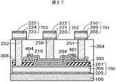
図7および図8は本発明の実施例1に基づく半導体装置の製造工程を示す断面図である。以下順を追って説明する。半導体素子が形成された基体100上に、スパッタ法を用い、膜厚50nmの窒化チタン膜からなる第一のバリア膜200、膜厚400nmのアルミニウム合金からなる第一のアルミニウム膜201、膜厚50nmの窒化チタン膜からなる第二のバリアメタル膜202を形成した後、プラズマCVD法を用い、膜厚100nmの酸化シリコンからなる第一の中間層300を形成し、リソグラフィー法とドライエッチ法を用いて第一の中間層300の所望の領域に第一の開口部500を形成した。次に、第一の開口部500を被覆するように反応性スパッタ法を用い、膜厚50nmの酸化タンタル膜からなる容量膜400、スパッタ法を用い、膜厚50nmの窒化チタンからなる上部電極203、プラズマCVD法を用い、膜厚100nmの酸化シリコンからなるハードマスク301を形成した(図7(a))。
7 and 8 are cross-sectional views showing the manufacturing steps of the semiconductor device according to the first embodiment of the present invention. The following will be described in order. A
次に、図7(b)に示すように、リソグラフィー法を用いてMIMキャパシタを形成したい領域を保護するように第一の加工レジスト600を形成し、この第一の加工レジスト600をエッチングマスクに、フッ素系ハロゲンガスを用いたドライエッチにより、加工されたハードマスク302、加工された上部電極204、加工された容量膜401を形成した。その後アッシャにより残った第一の加工レジスト600を除去した(図7(c))。この工程におけるドライエッチは、微細パターンの加工を伴わないため、容易にエッチングの終点判定が可能となる。また、万一、被加工物である容量膜400が部分的に残ったとしても、その後の工程において大きな問題となることはない。
Next, as shown in FIG. 7B, a first processing resist 600 is formed by using a lithography method so as to protect a region where the MIM capacitor is to be formed, and this first processing resist 600 is used as an etching mask. Then, a processed
次に、加工されたハードマスク302で被覆された領域以外において、金属配線を形成したい領域に対しリソグラフィー法を用いて、第二の加工レジスト601を形成し、この第二の加工レジスト601をエッチングマスクとして第一の中間層300をドライエッチした(図8(a))。引き続いて、メタルのエッチング装置を用いて、加工されたハードマスク302と第二の加工レジスト及びその直下にある加工された第一の中間層303をエッチングマスクとして塩素系のガスを用いたドライエッチングを行い、第一のバリアメタル層205、第一のアルミニウム層206、第二のバリアメタル層207によって構成される第一の金属配線700を形成し、第二の加工レジストをアッシャにより除去した(図8(b))。この工程において、寸法シフトの少ないハードマスクを加工マスクに用いているため、寸法制御性良く第一の金属配線700を加工することが可能となる。
Next, in a region other than the region covered with the processed
次に、図8(c)に示すように、プラズマCVD法を用いて膜厚1000nmの酸化シリコン膜からなる第一の層間絶縁層304を形成した後、化学的機械研磨法を用いて第一の層間絶縁層304の平坦化を行った。次に、リソグラフィー法とドライエッチング法を用いて、加工された上部電極204もしくは第一の金属配線700が露出するように開口部を設け、この開口部に対し、上部電極204と接続したタングステンからなる第一の導電性プラグ250、第一の金属配線700と接続したタングステンからなる第二の導電性プラグ251とを形成した。
Next, as shown in FIG. 8C, a first
最後に、スパッタ法及びリソグラフィー法、ドライエッチ法を組み合わせて所望の領域に膜厚50nmの窒化チタン膜からなる第三のバリア層208、膜厚400nmのアルミニウム合金からなる第二のアルミニウム層209、膜厚50nmの窒化チタン膜からなる第四のバリアメタル層210から構成される第二の金属配線701を形成した。以上の工程により、図1に示したような、第一の金属配線700、加工された容量膜401、上部電極204、第一の導電性プラグ250および第二の金属配線701から構成されるMIMキャパシタを有する半導体装置を形成することが可能となる。
Finally, a
上記の工程で形成したMIMキャパシタの平面レイアウト図を図9に示す。図1、図8、図9に示した断面図は図9中のA−A'間の断面である。図9におけるB−B'方向の断面図を図10に示した。図9に示したレイアウト図において、第一の中間層に設けられた開口部755がMIMキャパシタとして機能する領域である。MIMキャパシタ端部、すなわち、領域755の周縁部において、領域754であらわされる上部電極の直下には、膜厚100nmの酸化シリコンからなる第一の中間層303が形成されている。
この実施例1で示した構造のほかに、第一の中間層300の膜厚を0、10、50、200、300nmと変えて作成した構造もそれぞれ準備した。なお、ここで第一の中間層の厚みを0nmとした構造は、従来例2と本質的に同じ構造である。
FIG. 9 shows a planar layout of the MIM capacitor formed by the above process. The cross-sectional views shown in FIGS. 1, 8, and 9 are cross-sections along AA ′ in FIG. A cross-sectional view in the BB ′ direction in FIG. 9 is shown in FIG. In the layout diagram shown in FIG. 9, an
In addition to the structure shown in Example 1, structures prepared by changing the film thickness of the first
このようにして形成したMIMキャパシタを有する半導体装置におけるMIMキャパシタの性能と信頼度を調べた。その結果、第一の中間層の厚みにかかわらず、容量密度4fF/μm2が得られた。一方、MIMキャパシタを流れるリーク電流密度の電圧依存性を評価したところ、絶縁破壊耐圧の規格値(10Vの電圧でリーク電流密度が1平方センチメータあたり1μA以下)を満たしたのは、第一の中間層300の膜厚が50nmから200nmの間の構造を有するものであった。絶縁破壊耐圧が規格を満たさない理由を詳しく調べたところ、第一の中間層の膜厚が0nmと10nmのものでは、MIMキャパシタの端部において容量膜401の端部において下部電極700と上部電極204が容量膜401を挟んで直接対向している場合があることがわかった。このため、このMIM端部でのリーク電流の増大によって絶縁破壊耐圧が低下した可能性が考えられる。一方、第一の中間層の膜厚が300nmの場合には、第一の中間層の設けた開口部の端部付近で、容量膜400が局所的に薄くなっているのが観察された。これは、第一の中間層の膜厚が厚くなりすぎたために開口部端部での酸化タンタル膜のカバレジ不足が顕在化した可能性が考えられる。すなわち、第一の中間層が薄すぎると(たとえば10nm以下)、MIMキャパシタ端部におけるリーク電流増大を抑制する効果が失われ、一方、第一の中間層を厚くしすぎると(たとえば300nm以上)、開口部端部におけるスパッタカバレジが低下して、絶縁破壊耐圧が低下することがわかった。
次に、実施例1で示した構造のほかに、第一の層間絶縁膜としてプラズマCVD法を用いて形成したSiOC膜を用いた構造も準備した。このSiOC膜の比誘電率は2.9である。さらに比較のために、従来例3に示した工程図にもとづく構造も準備した。
The performance and reliability of the MIM capacitor in the semiconductor device having the MIM capacitor thus formed were examined. As a result, a capacitance density of 4 fF / μm 2 was obtained regardless of the thickness of the first intermediate layer. On the other hand, when the voltage dependency of the leakage current density flowing through the MIM capacitor was evaluated, the first value that satisfied the standard value of dielectric breakdown voltage (the leakage current density was 1 μA or less per square centimeter at a voltage of 10 V) The
Next, in addition to the structure shown in Example 1, a structure using a SiOC film formed by plasma CVD as a first interlayer insulating film was also prepared. The relative dielectric constant of this SiOC film is 2.9. For comparison, a structure based on the process diagram shown in Conventional Example 3 was also prepared.
このようにして形成したMIMキャパシタを有する半導体装置におけるMIMキャパシタの性能と信頼度を調べた。その結果、第一の層間絶縁膜の種類によらず容量密度4fF/μm2の性能と前記の規格値を満たす絶縁破壊耐圧が得られた。一方、第一の金属配線の寄生容量及び隣接する第一の金属配線間のリーク電流密度には差が生じた。図11に示したように、第一の層間絶縁膜にSiOC膜を用い、本実施例に基づき形成したMIMキャパシタでは隣接する配線間の寄生容量は対向長1cmあたり1.36pFとなるのに対し、従来例3にもとづいて形成した場合には1.56pFとなり、寄生容量が15%程度大きくなってしまい、回路動作の高速化、消費電力低減の妨げになる。一方、第一の層間絶縁膜に酸化シリコンを用いた場合には、実施例1と従来例3では寄生容量に大きな差は見られなかった。しかしながら、隣接する第一の金属配線700で形成した同層間櫛形キャパシタ構造で隣接配線間のショート歩留まりを評価したところ、従来例3に基づいて形成した場合には、ショート歩留まりが低下する傾向が得られた。
The performance and reliability of the MIM capacitor in the semiconductor device having the MIM capacitor thus formed were examined. As a result, regardless of the type of the first interlayer insulating film, a performance of a capacitance density of 4 fF / μm 2 and a dielectric breakdown voltage satisfying the standard value were obtained. On the other hand, a difference occurred in the parasitic capacitance of the first metal wiring and the leakage current density between the adjacent first metal wirings. As shown in FIG. 11, in the MIM capacitor formed based on this example using a SiOC film as the first interlayer insulating film, the parasitic capacitance between adjacent wirings is 1.36 pF per 1 cm of the opposing length. When formed based on the conventional example 3, it becomes 1.56 pF, and the parasitic capacitance increases by about 15%, which hinders high-speed circuit operation and low power consumption. On the other hand, when silicon oxide was used for the first interlayer insulating film, there was no significant difference in parasitic capacitance between Example 1 and Conventional Example 3. However, when the short-circuit yield between adjacent wirings was evaluated using the same inter-layer comb capacitor structure formed by the adjacent
つまり、本発明の実施例に従い、下部電極上に開口部を有する膜厚100nmの酸化シリコン層からなる第一の中間層を形成し、前記開口部を被覆するように容量膜、上部電極を形成し、前記開口部を完全に包含する形で上部電極、容量膜、第一の中間層、下部電極を加工することにより、リーク電流増大や絶縁破壊耐圧低下を最小限に抑制しつつ、高い容量密度が得られるMIMキャパシタと、このMIMキャパシタの下部電極に相当する配線層の寄生容量低減や配線間ショート歩留まりの向上が同時に可能となる半導体装置が形成可能となる。 That is, according to the embodiment of the present invention, a first intermediate layer made of a 100 nm-thickness silicon oxide layer having an opening is formed on the lower electrode, and a capacitor film and an upper electrode are formed so as to cover the opening. By processing the upper electrode, the capacitor film, the first intermediate layer, and the lower electrode so as to completely include the opening, a high capacity is achieved while minimizing an increase in leakage current and a decrease in dielectric breakdown voltage. It is possible to form a semiconductor device capable of simultaneously reducing the parasitic capacitance of the wiring layer corresponding to the lower electrode of the MIM capacitor and improving the short circuit yield between the wirings corresponding to the MIM capacitor capable of obtaining the density.
本実施例では、容量膜として膜厚50nmの酸化タンタルを用いたが、膜厚及び材料はこれに限定されるものではない。容量密度は容量膜の膜厚に反比例して増加するので、容量密度の面からは膜厚は薄いほど良い。ただし、薄膜化に応じて絶縁破壊耐圧も低下するので、使用する電圧に応じて薄膜化限界が存在する。また、容量膜の材料として、酸化タンタル以外にも酸化ハフニウム、酸化ジルコニウム、酸化ランタン、酸化チタン、酸化アルミなどやそれらの混合物およびそれらに窒素等が混入した化合物を用いることが可能である。また、PZT、STO、BST等の強誘電材料を用いることも可能である。さらに、本実施例では、容量膜として
単層の絶縁膜を用いているが、この容量膜は必要に応じて積層構造とすることも可能であり、たとえば、酸化タンタル膜の上下をバンドギャップの大きな酸化アルミ等で挟み込むことでリーク電流密度を下げることも可能となる。
In this embodiment, tantalum oxide having a film thickness of 50 nm is used as the capacitor film, but the film thickness and material are not limited thereto. Since the capacitance density increases in inverse proportion to the thickness of the capacitance film, the smaller the thickness, the better from the viewpoint of capacitance density. However, since the dielectric breakdown voltage also decreases as the film thickness is reduced, there is a thin film limit depending on the voltage used. In addition to tantalum oxide, it is possible to use hafnium oxide, zirconium oxide, lanthanum oxide, titanium oxide, aluminum oxide, a mixture thereof, and a compound in which nitrogen or the like is mixed therein as a material for the capacitor film. It is also possible to use a ferroelectric material such as PZT, STO, BST. Further, in this embodiment, a single-layer insulating film is used as the capacitive film. However, this capacitive film can have a laminated structure as required. For example, a band gap is formed above and below the tantalum oxide film. Leakage current density can be reduced by sandwiching with large aluminum oxide or the like.
また本実施例では、第一の中間層として主として膜厚100nmの酸化シリコン膜を用いているが、この膜厚、材料に限定されるものではない。前述のように第一の中間層には好適な膜厚範囲があり、現在の製造装置を用いている範囲では50nmから200nm程度が良好な特性が得られている。容量膜の形成方法としてより段差カバレジの良い手法を採用すれば、第一の中間層の上限が200nm以上の領域に広がることが容易に予想できるものの、いたずらにこの膜厚を増やすことに関してメリットは少ない。また、第一の中間層に用いる材料としてプラズマCVD法により形成した酸化シリコンを用いているが、当初の目的に合致する限りにおいて他の材料の選択を妨げるものではない。具体的には、窒化シリコン、酸窒化シリコン、炭化シリコン、窒素含有炭化シリコン、酸化アルミ、SiOCなどに代表されるLow−k膜などが利用可能である。窒化シリコンや酸窒化シリコン、酸化アルミを用いた場合には、ドライエッチ時の選択比向上やリソグラフィー時の吸光層として利用できるが、比誘電率が高いため配線の寄生容量が増大する欠点がある。一方、炭化シリコン、窒素含有炭化シリコン、SiOC膜などは比誘電率が低いために、寄生容量低減に効果的であるが、リーク電流が低減しにくい欠点もある。さらに、本実施例では、第一の中間層として単層の酸化シリコンを用いているが、これを複数の層からなる積層構造とすることも可能である。具体的には、下部電極に接する層として窒化シリコンを用い、その上層に酸化シリコンを用いた構造では、第一の中間層に設けた開口部の断面のテーパー角度を制御しやすくなる。このテーパー角度の制御性が良いと、容量膜のカバレジが向上しやすいため絶縁破壊耐圧の向上に効果的である。さらに、このテーパー角度の制御性が良ければ、MIMキャパシタの開口部面積の制御性が向上するので、所望の容量値が再現性良く得られるというメリットもある。 In this embodiment, a silicon oxide film having a film thickness of 100 nm is mainly used as the first intermediate layer, but the film thickness and material are not limited to these. As described above, the first intermediate layer has a preferable film thickness range, and good characteristics of about 50 nm to 200 nm are obtained in the range where the current manufacturing apparatus is used. If a method with better step coverage is adopted as a method of forming the capacitive film, the upper limit of the first intermediate layer can be easily expected to spread to a region of 200 nm or more, but there is no merit in increasing this film thickness unnecessarily. Few. Further, although silicon oxide formed by a plasma CVD method is used as the material used for the first intermediate layer, it does not hinder the selection of other materials as long as it meets the original purpose. Specifically, a low-k film typified by silicon nitride, silicon oxynitride, silicon carbide, nitrogen-containing silicon carbide, aluminum oxide, SiOC, or the like can be used. When silicon nitride, silicon oxynitride, or aluminum oxide is used, it can be used as a light-absorbing layer at the time of dry etching or at the time of lithography, but it has the disadvantage that the parasitic capacitance of the wiring increases due to its high dielectric constant. . On the other hand, silicon carbide, nitrogen-containing silicon carbide, SiOC film, and the like have a low relative dielectric constant and are effective in reducing parasitic capacitance, but have a drawback that leakage current is difficult to reduce. Furthermore, in this embodiment, a single layer of silicon oxide is used as the first intermediate layer, but it is also possible to form a laminated structure composed of a plurality of layers. Specifically, in a structure in which silicon nitride is used as a layer in contact with the lower electrode and silicon oxide is used as an upper layer, the taper angle of the cross section of the opening provided in the first intermediate layer can be easily controlled. When the controllability of the taper angle is good, coverage of the capacitive film is easily improved, which is effective in improving the breakdown voltage. Further, if the controllability of the taper angle is good, the controllability of the opening area of the MIM capacitor is improved, so that there is an advantage that a desired capacitance value can be obtained with good reproducibility.
また本実施例では、上部電極として膜厚50nmの窒化チタンを用いているが、膜厚、材料ともにこれに限定されない。上部電極が薄すぎる場合には接続孔を開口した場合に上部電極を突き破り、下に位置する容量膜に損傷を与える恐れがある。一方、膜厚が厚すぎる場合にはMIMキャパシタに対して直列に抵抗が挿入された形になるので、高周波特性が劣化する恐れがある。窒化チタンを用いている範囲では、50nmから100nm程度が好適である。また、上部電極の材料として、窒化チタン以外にタンタル、タングステン及びその窒化物を主たる成分とする金属、アルミおよびその合金、なども利用可能である。さらに、第一および第二の金属配線に用いるバリアメタルとして窒化チタンを用いているが、上記のように、窒化チタン以外にタンタル、タングステン及びその窒化物を主たる成分とする金属を用いることも可能であり、また、信頼度的に余裕があるのであれば、バリアメタルを用いない構造を利用することも可能である。また、上部電極、バリアメタルともに複数の層からなる積層構造にすることになんら問題はない。 In this embodiment, titanium nitride having a thickness of 50 nm is used as the upper electrode, but the thickness and material are not limited to this. If the upper electrode is too thin, the upper electrode may be pierced when the connection hole is opened, and the underlying capacitive film may be damaged. On the other hand, if the film thickness is too thick, a resistor is inserted in series with the MIM capacitor, so that the high frequency characteristics may be deteriorated. In the range where titanium nitride is used, about 50 nm to 100 nm is preferable. In addition to titanium nitride, tantalum, tungsten, and metals mainly composed of nitrides thereof, aluminum, alloys thereof, and the like can be used as upper electrode materials. Furthermore, titanium nitride is used as the barrier metal used for the first and second metal wirings. However, as described above, it is also possible to use a metal mainly composed of tantalum, tungsten, and nitride thereof in addition to titanium nitride. If there is a margin in reliability, it is possible to use a structure that does not use a barrier metal. In addition, there is no problem in forming a laminated structure including a plurality of layers for both the upper electrode and the barrier metal.
また本実施例では、図9のレイアウト図面に示したように、上部電極と上層配線は、開口部内に位置する1つの接続孔756で接続している。しかしながら、接続孔の位置、数、大きさはこの例に限定されることはない。接続孔の大きさは、大きければ大きいほど寄生抵抗は小さくなるため高周波特性は良好になる。しかし、一般的にCVD法で形成するタングステンの場合には、上限のサイズが存在する。接続孔の埋め込みをアルミ合金で行う場合には、このサイズ制限は緩和されるものの、別途、層間絶縁膜平坦化やメタル平坦化など工程数が増える原因となる。また本実施例では、接続孔位置が開口部の内側にある。この構成では上部電極にともなう寄生抵抗は最小限度に抑えられるものの、接続孔開口時のオーバーエッチ量が多すぎる場合には、容量膜に損傷が入る恐れがある。一方、接続孔を開口部の外側、つまり、図9において領域754内部で、かつ、領域755外部である領域、に設置した場合には、オーバーエッチに伴う容量膜損傷に対するマージンは大幅に向上する。その理由は、万一、接続孔が上部電極を突き抜けて容量膜に達しても、その直下には第一の中間層が存在するため、容量膜の損傷がそのままMIMキャパシタ特性の劣化につながらないからである。しかしながら、上部電極のシート抵抗に起因した寄生抵抗が増大するため、高周波特性には悪影響を与える恐れがある。また、図9のレイアウト図面では、MIMキャパシタは、ただ1つの第一の中間層に形成された開口部755をもつが、これを分割し、複数の開口部からなるMIMキャパシタとすることも可能である。
Further, in this embodiment, as shown in the layout drawing of FIG. 9, the upper electrode and the upper layer wiring are connected by one
また本実施例では、第一の層間絶縁膜として主として酸化シリコン膜を用いた工程を例に説明したが、この材料に限定されるわけではなく、配線の寄生容量が低減可能なLow−k材料を用いることも可能である。Low−k材料としては、ブラックダイアモンド(登録商標:Applied Materials社製)に代表されるようなSiOC膜(炭素を含有する酸化シリコン膜)、SiLK(登録商標:Dow Chemical社製)に代表されるような有機膜、およびそれらに空隙を導入したLow−k材料、フッ素含有酸化シリコン膜などを用いることが可能である。この酔うなLow−k材料を用いるときには、何らかの保護絶縁膜が必要であるので、第一の層間絶縁膜としては、それら複数の絶縁膜から構成される積層膜も含んでいる。さらにこのようなLow−k材料を用いた場合には、プロセス温度等の制約からタングステンのCVD法の適用が困難な場合が多いので、その際にはアルミ等で接続孔を埋め込んだほうが良い。
本実施例では、第二の金属配線をドライエッチ法で加工したアルミ配線を用いているが、必要に応じてダマシン法を用いたアルミ配線や銅配線を用いることも可能である。この際、接続孔も同時に形成するデュアルダマシン法を適用し、工程数を削減することも可能である。
In this embodiment, the process using mainly a silicon oxide film as the first interlayer insulating film has been described as an example. However, the present invention is not limited to this material, and a low-k material capable of reducing the parasitic capacitance of the wiring. It is also possible to use. As a Low-k material, a SiOC film (silicon oxide film containing carbon) represented by black diamond (registered trademark: Applied Materials), and SiLK (registered trademark: manufactured by Dow Chemical) are representative. Such organic films, Low-k materials in which voids are introduced, fluorine-containing silicon oxide films, and the like can be used. When this intoxicating Low-k material is used, some kind of protective insulating film is required. Therefore, the first interlayer insulating film includes a laminated film composed of the plurality of insulating films. Further, when such a low-k material is used, it is often difficult to apply the tungsten CVD method due to restrictions such as process temperature. In this case, it is preferable to bury the connection hole with aluminum or the like.
In this embodiment, an aluminum wiring obtained by processing the second metal wiring by the dry etching method is used, but an aluminum wiring or a copper wiring using a damascene method can be used as necessary. At this time, it is possible to reduce the number of processes by applying a dual damascene method in which connection holes are formed at the same time.
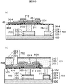
図12および図13は本発明の半導体装置の製造工程を示す断面図である。以下、順を追って説明する。 12 and 13 are cross-sectional views showing the manufacturing process of the semiconductor device of the present invention. In the following, description will be given in order.
図12(a)に示すように、半導体素子が形成された基体100上に、スパッタ法を用い、膜厚50nmの窒化チタン膜からなる第一のバリア膜200、膜厚400nmのアルミニウム合金からなる第一のアルミニウム膜201、膜厚50nmの窒化チタン膜からなる第二のバリアメタル膜202を形成した後、プラズマCVD法を用い、膜厚100nmの酸化シリコンからなる第一の中間層300を形成し、リソグラフィー法とドライエッチ法を用いて第一の中間層300の所望の領域に開口部を設けた後、この開口部を被覆するように、反応性スパッタ法を用い、膜厚50nmの酸化タンタル膜からなる容量膜400、スパッタ法を用い、膜厚50nmの窒化チタンからなる上部電極203を形成した。その後、リソグラフィー法を用いてMIMキャパシタを形成したい領域を保護するように第一の加工レジスト600を形成した。
As shown in FIG. 12A, a
次に、この第一の加工レジスト600をエッチングマスクに、フッ素系ハロゲンガスを用いたドライエッチにより、加工された上部電極204、加工された容量膜401を形成した後、アッシャにより残った第一の加工レジスト600を除去した。その後、MIMキャパシタを形成したい領域と金属配線を形成したい領域とを保護するように、リソグラフィー法を用いて、第二の加工レジスト601を形成した(図12(b))。
次に、この第二の加工レジスト601をエッチングマスクとして、第一の中間層300をドライエッチした。引き続いて、メタルのエッチング装置を用いてドライエッチを行い、第二の加工レジスト601をエッチングマスクとして、第一のバリアメタル層205、第一のアルミニウム層206、第二のバリアメタル層207によって構成される第一の金属配線700を形成した(図12(c))。
Next, the processed
Next, the first
次に、図13(a)に示すように、第二の加工レジスト601をアッシャで除去後、プラズマCVD法を用いて膜厚1000nmの酸化シリコン膜からなる第一の層間絶縁層304を形成した後、化学的機械研磨法を用いて第一の層間絶縁層304の平坦化を行った。次に、リソグラフィー法とドライエッチング法を用いて、加工された上部電極204もしくは第一の金属配線700が露出するように開口部を設け、この開口部に対し、上部電極204と接続したタングステンからなる第一の導電性プラグ250、第一の金属配線700と接続したタングステンからなる第二の導電性プラグ251とを形成した。
Next, as shown in FIG. 13A, after the second processing resist 601 is removed by an asher, a first
最後に、スパッタ法及びリソグラフィー法、ドライエッチ法を組み合わせて所望の領域に膜厚50nmの窒化チタン膜からなる第三のバリア層208、膜厚400nmのアルミニウム合金からなる第二のアルミニウム層209、膜厚50nmの窒化チタン膜からなる第四のバリアメタル層210から構成される第二の金属配線701を形成した。以上の工程により、図13(b)に示したような、第一の金属配線700、加工された容量膜401、上部電極204、第一の導電性プラグ250および第二の金属配線701から構成されるMIMキャパシタを有する半導体装置を形成することが可能となる。
この実施例2で示した構造のほかに、第一の層間絶縁膜としてプラズマCVD法を用いて形成したSiOC膜を用いた構造も準備した。
Finally, a
In addition to the structure shown in Example 2, a structure using a SiOC film formed by plasma CVD as a first interlayer insulating film was also prepared.
このようにして形成したMIMキャパシタを有する半導体装置におけるMIMキャパシタの性能と信頼度を調べた結果、実施例1に示したのと同等の容量密度、絶縁破壊耐圧の規格値が得られた。また隣接する第一の金属配線間の寄生容量およびショート歩留まりも実施例1と同等の値が得られた。
つまり、本発明の実施例に従い、下部電極上に開口部を有する膜厚100nmの酸化シリコン層からなる第一の中間層を形成し、前記開口部を被覆するように容量膜、上部電極を形成し、前記開口部を完全に包含する形で上部電極、容量膜、第一の中間層、下部電極を加工することにより、リーク電流増大や絶縁破壊耐圧低下を最小限に抑制しつつ、高い容量密度が得られるMIMキャパシタと、このMIMキャパシタの下部電極に相当する配線層の寄生容量低減や配線間ショート歩留まりの向上が同時に可能となる半導体装置が形成可能となる。
As a result of investigating the performance and reliability of the MIM capacitor in the semiconductor device having the MIM capacitor formed as described above, the standard values of the capacitance density and the dielectric breakdown voltage equivalent to those shown in Example 1 were obtained. In addition, the parasitic capacitance between the adjacent first metal wirings and the short yield were also the same values as in Example 1.
That is, according to the embodiment of the present invention, a first intermediate layer made of a 100 nm-thickness silicon oxide layer having an opening is formed on the lower electrode, and a capacitor film and an upper electrode are formed so as to cover the opening. By processing the upper electrode, the capacitor film, the first intermediate layer, and the lower electrode so as to completely include the opening, a high capacity is achieved while minimizing an increase in leakage current and a decrease in dielectric breakdown voltage. It is possible to form a semiconductor device capable of simultaneously reducing the parasitic capacitance of the wiring layer corresponding to the lower electrode of the MIM capacitor and improving the short circuit yield between the wirings corresponding to the MIM capacitor capable of obtaining the density.
本実施例では、実施例1と異なり、MIMキャパシタ直下の積層アルミ膜の加工にレジストマスクを用いている。ハードマスクを用いていないため、微細加工時の寸法制御性の面で若干不利ではあるものの、ハードマスク成膜工程が省略できるというメリットがある。
本実施例では、容量膜として膜厚50nmの酸化タンタルを用いたが、膜厚及び材料はこれに限定されるものではない。容量密度は容量膜の膜厚に反比例して増加するので、容量密度の面からは膜厚は薄いほど良い。ただし、薄膜化に応じて絶縁破壊耐圧も低下するので、使用する電圧に応じて薄膜化限界が存在する。また、容量膜の材料として、酸化タンタル以外にも酸化ハフニウム、酸化ジルコニウム、酸化ランタン、酸化チタン、酸化アルミなどやそれらの混合物およびそれらに窒素等が混入した化合物を用いることが可能である。また、PZT、STO、BST等の強誘電材料を用いることも可能である。さらに、本実施例では、容量膜として単層の絶縁膜を用いているが、この容量膜は必要に応じて積層構造とすることも可能であり、たとえば、酸化タンタル膜の上下をバンドギャップの大きな酸化アルミ等で挟み込むことでリーク電流密度を下げることも可能となる。
In this embodiment, unlike the first embodiment, a resist mask is used for processing the laminated aluminum film directly under the MIM capacitor. Since a hard mask is not used, there is a merit that the hard mask film forming step can be omitted, although it is slightly disadvantageous in terms of dimensional controllability during microfabrication.
In this embodiment, tantalum oxide having a film thickness of 50 nm is used as the capacitor film, but the film thickness and material are not limited thereto. Since the capacitance density increases in inverse proportion to the thickness of the capacitance film, the smaller the thickness, the better from the viewpoint of capacitance density. However, since the dielectric breakdown voltage also decreases as the film thickness is reduced, there is a thin film limit depending on the voltage used. In addition to tantalum oxide, it is possible to use hafnium oxide, zirconium oxide, lanthanum oxide, titanium oxide, aluminum oxide, a mixture thereof, and a compound in which nitrogen or the like is mixed therein as a material for the capacitor film. It is also possible to use a ferroelectric material such as PZT, STO, BST. Further, in this embodiment, a single-layer insulating film is used as the capacitive film. However, this capacitive film can have a laminated structure as required. For example, a band gap is formed above and below the tantalum oxide film. Leakage current density can be reduced by sandwiching with large aluminum oxide or the like.
また本実施例では、第一の中間層として主として膜厚100nmの酸化シリコン膜を用いているが、この膜厚、材料に限定されるものではない。前述のように第一の中間層には好適な膜厚範囲があり、現在の製造装置を用いている範囲では50nmから200nm程度が良好な特性が得られている。容量膜の形成方法としてより段差カバレジの良い手法を採用すれば、第一の中間層の上限が200nm以上の領域に広がることが容易に予想できるものの、いたずらにこの膜厚を増やすことに関してメリットは少ない。また、第一の中間層に用いる材料としてプラズマCVD法により形成した酸化シリコンを用いているが、当初の目的に合致する限りにおいて他の材料の選択を妨げるものではない。具体的には、窒化シリコン、酸窒化シリコン、炭化シリコン、窒素含有炭化シリコン、酸化アルミ、SiOCなどに代表されるLow−k膜などが利用可能である。窒化シリコンや酸窒化シリコン、酸化アルミを用いた場合には、ドライエッチ時の選択比向上やリソグラフィー時の吸光層として利用できるが、比誘電率が高いため配線の寄生容量が増大する欠点がある。一方、炭化シリコン、窒素含有炭化シリコン、SiOC膜などは比誘電率が低いために、寄生容量低減に効果的であるが、リーク電流が低減しにくい欠点もある。さらに、本実施例では、第一の中間層として単層の酸化シリコンを用いているが、これを複数の層からなる積層構造とすることも可能である。具体的には、下部電極に接する層として窒化シリコンを用い、その上層に酸化シリコンを用いた構造では、第一の中間層に設けた開口部の断面のテーパー角度を制御しやすくなる。このテーパー角度の制御性が良いと、容量膜のカバレジが向上しやすいため絶縁破壊耐圧の向上に効果的である。さらに、このテーパー角度の制御性が良ければ、MIMキャパシタの開口部面積の制御性が向上するので、所望の容量値が再現性良く得られるというメリットもある。 In this embodiment, a silicon oxide film having a film thickness of 100 nm is mainly used as the first intermediate layer, but the film thickness and material are not limited to these. As described above, the first intermediate layer has a preferable film thickness range, and good characteristics of about 50 nm to 200 nm are obtained in the range where the current manufacturing apparatus is used. If a method with better step coverage is adopted as a method of forming the capacitive film, the upper limit of the first intermediate layer can be easily expected to spread to a region of 200 nm or more, but there is no merit in increasing this film thickness unnecessarily. Few. Further, although silicon oxide formed by a plasma CVD method is used as the material used for the first intermediate layer, it does not hinder the selection of other materials as long as it meets the original purpose. Specifically, a low-k film typified by silicon nitride, silicon oxynitride, silicon carbide, nitrogen-containing silicon carbide, aluminum oxide, SiOC, or the like can be used. When silicon nitride, silicon oxynitride, or aluminum oxide is used, it can be used as a light-absorbing layer at the time of dry etching or at the time of lithography, but it has the disadvantage that the parasitic capacitance of the wiring increases due to its high dielectric constant. . On the other hand, silicon carbide, nitrogen-containing silicon carbide, SiOC film, and the like have a low relative dielectric constant and are effective in reducing parasitic capacitance, but have a drawback that leakage current is difficult to reduce. Furthermore, in this embodiment, a single layer of silicon oxide is used as the first intermediate layer, but it is also possible to form a laminated structure composed of a plurality of layers. Specifically, in a structure in which silicon nitride is used as a layer in contact with the lower electrode and silicon oxide is used as an upper layer, the taper angle of the cross section of the opening provided in the first intermediate layer can be easily controlled. When the controllability of the taper angle is good, coverage of the capacitive film is easily improved, which is effective in improving the breakdown voltage. Further, if the controllability of the taper angle is good, the controllability of the opening area of the MIM capacitor is improved, so that there is an advantage that a desired capacitance value can be obtained with good reproducibility.
また本実施例では、上部電極として膜厚50nmの窒化チタンを用いているが、膜厚、材料ともにこれに限定されない。上部電極が薄すぎる場合には接続孔を開口した場合に上部電極を突き破り、下に位置する容量膜に損傷を与える恐れがある。一方、膜厚が厚すぎる場合にはMIMキャパシタに対して直列に抵抗が挿入された形になるので、高周波特性が劣化する恐れがある。窒化チタンを用いている範囲では、50nmから100nm程度が好適である。また、上部電極の材料として、窒化チタン以外にタンタル、タングステン及びその窒化物を主たる成分とする金属、アルミおよびその合金、なども利用可能である。さらに、第一および第二の金属配線に用いるバリアメタルとして窒化チタンを用いているが、上記のように、窒化チタン以外にタンタル、タングステン及びその窒化物を主たる成分とする金属を用いることも可能であり、また、信頼度的に余裕があるのであれば、バリアメタルを用いない構造を利用することも可能である。また、上部電極、バリアメタルともに複数の層からなる積層構造にすることになんら問題はない。 In this embodiment, titanium nitride having a thickness of 50 nm is used as the upper electrode, but the thickness and material are not limited to this. If the upper electrode is too thin, the upper electrode may be pierced when the connection hole is opened, and the underlying capacitive film may be damaged. On the other hand, if the film thickness is too thick, a resistor is inserted in series with the MIM capacitor, so that the high frequency characteristics may be deteriorated. In the range where titanium nitride is used, about 50 nm to 100 nm is preferable. In addition to titanium nitride, tantalum, tungsten, and metals mainly composed of nitrides thereof, aluminum, alloys thereof, and the like can be used as upper electrode materials. Furthermore, titanium nitride is used as the barrier metal used for the first and second metal wirings. However, as described above, it is also possible to use a metal mainly composed of tantalum, tungsten, and nitride thereof in addition to titanium nitride. If there is a margin in reliability, it is possible to use a structure that does not use a barrier metal. In addition, there is no problem in forming a laminated structure including a plurality of layers for both the upper electrode and the barrier metal.
また本実施例では、実施例1とほぼ同様、図9のレイアウト図面に示したような構成をとっている。ただ、実施例とは一点異なっており、上部電極を示す領域754の外側に第一の金属配線750が位置している。実際の応用を考えた場合には、実施例2に示したような、接続孔の位置、数、大きさに限定されることはない。接続孔の大きさは、大きければ大きいほど寄生抵抗は小さくなるため高周波特性は良好になる。しかし、一般的にCVD法で形成するタングステンの場合には、上限のサイズが存在する。接続孔の埋め込みをアルミ合金で行う場合には、このサイズ制限は緩和されるものの、別途、層間絶縁膜平坦化やメタル平坦化など工程数が増える原因となる。また本実施例では、接続孔位置が開口部の内側にある。この構成では上部電極にともなう寄生抵抗は最小限度に抑えられるものの、接続孔開口時のオーバーエッチ量が多すぎる場合には、容量膜に損傷が入る恐れがある。一方、接続孔を開口部の外側、つまり、図9において領域754内部で、かつ、領域755外部である領域、に設置した場合には、オーバーエッチに伴う容量膜損傷に対するマージンは大幅に向上する。その理由は、万一、接続孔が上部電極を突き抜けて容量膜に達しても、その直下には第一の中間層が存在するため、容量膜の損傷がそのままMIMキャパシタ特性の劣化につながらないからである。しかしながら、上部電極のシート抵抗に起因した寄生抵抗が増大するため、高周波特性には悪影響を与える恐れがある。
Further, in this embodiment, the configuration shown in the layout drawing of FIG. However, it is different from the embodiment in that the
また本実施例では、第一の層間絶縁膜として主として酸化シリコン膜を用いた工程を例に説明したが、この材料に限定されるわけではなく、配線の寄生容量が低減可能なLow−k材料を用いることも可能である。Low−k材料としては、ブラックダイアモンド(登録商標:Applied Materials社製)に代表されるようなSiOC膜(炭素を含有する酸化シリコン膜)、SiLK(登録商標:Dow Chemical社製)に代表されるような有機膜、およびそれらに空隙を導入したLow−k材料、フッ素含有酸化シリコン膜などを用いることが可能である。この酔うなLow−k材料を用いるときには、何らかの保護絶縁膜が必要であるので、第一の層間絶縁膜としては、それら複数の絶縁膜から構成される積層膜も含んでいる。さらにこのようなLow−k材料を用いた場合には、プロセス温度等の制約からタングステンのCVD法の適用が困難な場合が多いので、その際にはアルミ等で接続孔を埋め込んだほうが良い。
本実施例では、第二の金属配線をドライエッチ法で加工したアルミ配線を用いているが、必要に応じてダマシン法を用いたアルミ配線や銅配線を用いることも可能である。この際、接続孔も同時に形成するデュアルダマシン法を適用し、工程数を削減することも可能である。
In this embodiment, the process using mainly a silicon oxide film as the first interlayer insulating film has been described as an example. However, the present invention is not limited to this material, and a low-k material capable of reducing the parasitic capacitance of the wiring. It is also possible to use. As a Low-k material, a SiOC film (silicon oxide film containing carbon) represented by black diamond (registered trademark: Applied Materials), and SiLK (registered trademark: manufactured by Dow Chemical) are representative. Such organic films, Low-k materials in which voids are introduced, fluorine-containing silicon oxide films, and the like can be used. When this intoxicating Low-k material is used, some kind of protective insulating film is required. Therefore, the first interlayer insulating film includes a laminated film composed of the plurality of insulating films. Further, when such a low-k material is used, it is often difficult to apply the tungsten CVD method due to restrictions such as process temperature. In this case, it is preferable to bury the connection hole with aluminum or the like.
In this embodiment, an aluminum wiring obtained by processing the second metal wiring by the dry etching method is used, but an aluminum wiring or a copper wiring using a damascene method can be used as necessary. At this time, it is also possible to reduce the number of processes by applying a dual damascene method in which connection holes are formed simultaneously.
図14および図15は本発明の半導体装置の製造工程を示す断面図である。以下、順を追って説明する。
図14(a)に示すように、半導体素子が形成された基体100上に、スパッタ法を用い、膜厚50nmの窒化チタン膜、膜厚400nmのアルミニウム合金、膜厚50nmの窒化チタン膜を形成した後、リソグラフィー法とドライエッチ法を用いて第一のバリアメタル層205、第一のアルミニウム層206、第二のバリアメタル層207によって構成される第一の金属配線700を形成した。次に、プラズマCVD法を用いて膜厚1000nmの酸化シリコン膜からなる第一の層間絶縁層304を形成した後、化学的機械研磨法を用いて第一の層間絶縁層304の平坦化を行った。次に、リソグラフィー法とドライエッチング法を用いて、所望の領域の第一の金属配線700が露出するように開口部を設け、この開口部に対し、タングステンからなる第一の導電性プラグ250、第二の導電性プラグ251とを形成した。次に、この第一の導電性プラグ250、第二の導電性プラグ251を被覆するようにスパッタ法を用いて膜厚50nmの窒化チタンを形成し、リソグラフィー法とドライエッチ法とを組み合わせて、第一の導電性プラグ250を被覆するように加工された下部電極211を形成した。その後、プラズマCVD法を用いて膜厚100nmの酸化シリコン膜を形成した後、リソグラフィー法とドライエッチ法を用い、加工された下部電極211に開口部500を有する第一の中間層300を形成した。
14 and 15 are cross-sectional views showing the manufacturing process of the semiconductor device of the present invention. In the following, description will be given in order.
As shown in FIG. 14A, a 50-nm-thick titanium nitride film, a 400-nm-thick aluminum alloy, and a 50-nm-thick titanium nitride film are formed on a
次に、この開口部500を被覆し、かつ、加工された下部電極211と接するように膜厚50nmの酸化タンタルからなる容量膜400を形成し、さらにスパッタ法で膜厚50nmの窒化チタンからなる上部電極203を形成した。その後、MIMキャパシタとして残したい領域をカバーするように第一の加工レジスト600をリソグラフィー法を用いて形成した(図14(b))。
次に、第一の加工レジスト600を加工マスクとして、上部電極203、容量膜400、第一の中間層300をドライエッチした。その後、全面にスパッタ法で、膜厚50nmの窒化チタン膜からなる第三のバリア膜212、膜厚400nmのアルミニウム合金からなる第二のアルミニウム膜213、膜厚50nmの窒化チタン膜からなる第四のバリアメタル膜214を形成した(図15(a))。
Next, a
Next, the
次に図15(b)に示すように、金属配線を形成したい領域に、第二の加工レジスト601をリソグラフィー法で形成し、塩素系のガスを用いたドライエッチ法により、膜厚50nmの窒化チタン膜からなる第三のバリア層208、膜厚400nmのアルミニウム合金からなる第二のアルミニウム層209、膜厚50nmの窒化チタン膜からなる第四のバリアメタル層210から構成される第二の金属配線701を形成した。最後に余分な第二の加工レジスト601をアッシャで除去することで、第一の金属配線700、第一の導電性プラグ250、加工された下部電極211、加工された容量膜401、加工された上部電極204、および第二の金属配線701から構成されるMIMキャパシタを有する半導体装置を形成することが可能となる。
この実施例3で示した構造のほかに、第一の中間層300の膜厚を0、10、50、200、300nmと変えて作成した構造もそれぞれ準備した。
Next, as shown in FIG. 15B, a second processed resist 601 is formed by lithography in a region where metal wiring is to be formed, and nitrided to a thickness of 50 nm by dry etching using a chlorine-based gas. A second metal composed of a
In addition to the structure shown in Example 3, structures prepared by changing the thickness of the first
このようにして形成したMIMキャパシタを有する半導体装置におけるMIMキャパシタの性能と信頼度を調べた。その結果、実施例1と同様、第一の中間層の厚みにかかわらず、容量密度4fF/μm2の性能が得られた。一方、MIMキャパシタの絶縁破壊耐圧の規格値を満たしたのは、実施例1と同様、第一の中間層300の膜厚が50nmから200nmの間の構造を有するものであった。絶縁破壊耐圧が規格を満たさない理由を詳しく調べたところ、第一の中間層の膜厚が0nmと10nmのものでは、下部電極211の端部および側壁においてその上に形成された第一の中間層や容量膜が薄くなっていることがわかった。このため、この下部電極端部におけるリーク電流の増大によって絶縁破壊耐圧が低下した可能性が考えられる。一方、第一の中間層の膜厚が300nmの場合には、第一の中間層303に設けた開口部の端部付近で、容量膜400が局所的に薄くなっているのが観察された。これは、第一の中間層の膜厚が厚くなりすぎたために開口部端部での酸化タンタル膜のカバレジ不足が顕在化した可能性が考えられる。すなわち、第一の中間層が薄すぎると(たとえば10nm以下)、MIMキャパシタ端部におけるリーク電流増大を抑制する効果が失われ、一方、第一の中間層を厚くしすぎると(たとえば300nm以上)、開口部端部におけるスパッタカバレジが低下して、絶縁破壊耐圧が低下することがわかった。
The performance and reliability of the MIM capacitor in the semiconductor device having the MIM capacitor thus formed were examined. As a result, similar to Example 1, a performance with a capacitance density of 4 fF / μm 2 was obtained regardless of the thickness of the first intermediate layer. On the other hand, the reason why the standard value of the dielectric breakdown voltage of the MIM capacitor was satisfied was that the film thickness of the first
さらに、実施例1と同様、第一の金属配線700、第二の金属配線701の周囲を比誘電率の高い第一の中間層で被覆されることがないため、従来例3のように配線の寄生容量が増大し、信号遅延の増大や消費電力の増大といった問題がおきにくいことがわかった。
つまり、本発明の実施例に従い、下層金属配線に開口された接続孔を被覆するように下部電極を形成し、この下部電極上に開口部を有する膜厚100nmの酸化シリコン層からなる第一の中間層を形成し、前記開口部を被覆するように容量膜、上部電極を形成し、前記開口部を完全に包含する形で上部電極、容量膜、第一の中間層を加工することにより、リーク電流増大や絶縁破壊耐圧低下を最小限に抑制しつつ、高い容量密度が得られるMIMキャパシタを有する半導体装置が形成可能となる。
Further, as in the first embodiment, the periphery of the
That is, according to the embodiment of the present invention, the lower electrode is formed so as to cover the connection hole opened in the lower layer metal wiring, and the first oxide film is formed of a 100 nm-thickness silicon oxide layer having an opening on the lower electrode. By forming an intermediate layer, forming a capacitive film and an upper electrode so as to cover the opening, and processing the upper electrode, the capacitive film, and the first intermediate layer in a form completely including the opening, A semiconductor device having an MIM capacitor capable of obtaining a high capacitance density while minimizing an increase in leakage current and a decrease in dielectric breakdown voltage can be formed.
本実施例では、実施例1と異なり、MIMキャパシタの容量膜直下はアルミ配線とは別個に形成した金属膜であるので、アルミ配線に使われているバリアメタルとは独立して材料選択が可能であり、また、アルミ配線上に生じるヒロック等の影響を受けにくい特徴を持つ。一方、下部電極の加工工程が新たに加わるので全体の工程数は増加する。
本実施例では、容量膜として膜厚50nmの酸化タンタルを用いたが、膜厚及び材料はこれに限定されるものではない。容量密度は容量膜の膜厚に反比例して増加するので、容量密度の面からは膜厚は薄いほど良い。ただし、薄膜化に応じて絶縁破壊耐圧も低下するので、使用する電圧に応じて薄膜化限界が存在する。また、容量膜の材料として、酸化タンタル以外にも酸化ハフニウム、酸化ジルコニウム、酸化ランタン、酸化チタン、酸化アルミなどやそれらの混合物およびそれらに窒素等が混入した化合物を用いることが可能である。また、PZT、STO、BST等の強誘電材料を用いることも可能である。さらに、本実施例では、容量膜として単層の絶縁膜を用いているが、この容量膜は必要に応じて積層構造とすることも可能であり、たとえば、酸化タンタル膜の上下をバンドギャップの大きな酸化アルミ等で挟み込むことでリーク電流密度を下げることも可能となる。
In the present embodiment, unlike the first embodiment, the material film directly under the capacitance film of the MIM capacitor is a metal film formed separately from the aluminum wiring, so that the material can be selected independently of the barrier metal used in the aluminum wiring. In addition, it has the characteristic that it is not easily affected by hillocks and the like generated on the aluminum wiring. On the other hand, since the lower electrode processing step is newly added, the total number of steps increases.
In this embodiment, tantalum oxide having a film thickness of 50 nm is used as the capacitor film, but the film thickness and material are not limited thereto. Since the capacitance density increases in inverse proportion to the thickness of the capacitance film, the smaller the thickness, the better from the viewpoint of capacitance density. However, since the dielectric breakdown voltage also decreases as the film thickness is reduced, there is a thin film limit depending on the voltage used. In addition to tantalum oxide, it is possible to use hafnium oxide, zirconium oxide, lanthanum oxide, titanium oxide, aluminum oxide, a mixture thereof, and a compound in which nitrogen or the like is mixed therein as a material for the capacitor film. It is also possible to use a ferroelectric material such as PZT, STO, BST. Further, in this embodiment, a single-layer insulating film is used as the capacitive film. However, this capacitive film can have a laminated structure as required. For example, a band gap is formed above and below the tantalum oxide film. Leakage current density can be reduced by sandwiching with large aluminum oxide or the like.
また本実施例では、第一の中間層として主として膜厚100nmの酸化シリコン膜を用いているが、この膜厚、材料に限定されるものではない。前述のように第一の中間層には好適な膜厚範囲があり、現在の製造装置を用いている範囲では50nmから200nm程度が良好な特性が得られている。容量膜の形成方法としてより段差カバレジの良い手法を採用すれば、第一の中間層の上限が200nm以上の領域に広がることが容易に予想できるものの、いたずらにこの膜厚を増やすことに関してメリットは少ない。また、第一の中間層に用いる材料としてプラズマCVD法により形成した酸化シリコンを用いているが、当初の目的に合致する限りにおいて他の材料の選択を妨げるものではない。具体的には、窒化シリコン、酸窒化シリコン、炭化シリコン、窒素含有炭化シリコン、酸化アルミ、SiOCなどに代表されるLow−k膜などが利用可能である。窒化シリコンや酸窒化シリコン、酸化アルミを用いた場合には、ドライエッチ時の選択比向上やリソグラフィー時の吸光層として利用できるが、比誘電率が高いため配線の寄生容量が増大する欠点がある。一方、炭化シリコン、窒素含有炭化シリコン、SiOC膜などは比誘電率が低いために、寄生容量低減に効果的であるが、リーク電流が低減しにくい欠点もある。さらに、本実施例では、第一の中間層として単層の酸化シリコンを用いているが、これを複数の層からなる積層構造とすることも可能である。具体的には、下部電極に接する層として窒化シリコンを用い、その上層に酸化シリコンを用いた構造では、第一の中間層に設けた開口部の断面のテーパー角度を制御しやすくなる。このテーパー角度の制御性が良いと、容量膜のカバレジが向上しやすいため絶縁破壊耐圧の向上に効果的である。さらに、このテーパー角度の制御性が良ければ、MIMキャパシタの開口部面積の制御性が向上するので、所望の容量値が再現性良く得られるというメリットもある。 In this embodiment, a silicon oxide film having a film thickness of 100 nm is mainly used as the first intermediate layer, but the film thickness and material are not limited to these. As described above, the first intermediate layer has a preferable film thickness range, and good characteristics of about 50 nm to 200 nm are obtained in the range where the current manufacturing apparatus is used. If a method with better step coverage is adopted as a method of forming the capacitive film, the upper limit of the first intermediate layer can be easily expected to spread to a region of 200 nm or more, but there is no merit in increasing this film thickness unnecessarily. Few. Further, although silicon oxide formed by a plasma CVD method is used as the material used for the first intermediate layer, it does not hinder the selection of other materials as long as it meets the original purpose. Specifically, a low-k film typified by silicon nitride, silicon oxynitride, silicon carbide, nitrogen-containing silicon carbide, aluminum oxide, SiOC, or the like can be used. When silicon nitride, silicon oxynitride, or aluminum oxide is used, it can be used as a light-absorbing layer at the time of dry etching or at the time of lithography, but it has the disadvantage that the parasitic capacitance of the wiring increases due to its high dielectric constant. . On the other hand, silicon carbide, nitrogen-containing silicon carbide, SiOC film, and the like have a low relative dielectric constant and are effective in reducing parasitic capacitance, but have a drawback that leakage current is difficult to reduce. Furthermore, in this embodiment, a single layer of silicon oxide is used as the first intermediate layer, but it is also possible to form a laminated structure composed of a plurality of layers. Specifically, in a structure in which silicon nitride is used as a layer in contact with the lower electrode and silicon oxide is used as an upper layer, the taper angle of the cross section of the opening provided in the first intermediate layer can be easily controlled. When the controllability of the taper angle is good, coverage of the capacitive film is easily improved, which is effective in improving the breakdown voltage. Further, if the controllability of the taper angle is good, the controllability of the opening area of the MIM capacitor is improved, so that there is an advantage that a desired capacitance value can be obtained with good reproducibility.
また本実施例では、下部電極及び上部電極として膜厚50nmの窒化チタンを用いているが、膜厚、材料ともにこれに限定されない。電極膜厚が厚すぎる場合にはMIMキャパシタに対して直列に抵抗が挿入された形になるので、高周波特性が劣化する恐れがある。窒化チタンを用いている範囲では、50nmから100nm程度が好適である。また、上部電極の材料として、窒化チタン以外にタンタル、タングステン及びその窒化物を主たる成分とする金属、アルミおよびその合金、なども利用可能である。さらに、第一および第二の金属配線に用いるバリアメタルとして窒化チタンを用いているが、上記のように、窒化チタン以外にタンタル、タングステン及びその窒化物を主たる成分とする金属を用いることも可能であり、また、信頼度的に余裕があるのであれば、バリアメタルを用いない構造を利用することも可能である。また、上部電極、バリアメタルともに複数の層からなる積層構造にすることになんら問題はない。 In this embodiment, titanium nitride having a thickness of 50 nm is used as the lower electrode and the upper electrode, but the thickness and material are not limited to this. When the electrode film thickness is too thick, a resistor is inserted in series with the MIM capacitor, so that the high frequency characteristics may be deteriorated. In the range where titanium nitride is used, about 50 nm to 100 nm is preferable. In addition to titanium nitride, tantalum, tungsten, and metals mainly composed of nitrides thereof, aluminum, alloys thereof, and the like can be used as upper electrode materials. Furthermore, titanium nitride is used as the barrier metal used for the first and second metal wirings. However, as described above, it is also possible to use a metal mainly composed of tantalum, tungsten, and nitride thereof in addition to titanium nitride. If there is a margin in reliability, it is possible to use a structure that does not use a barrier metal. In addition, there is no problem in forming a laminated structure including a plurality of layers for both the upper electrode and the barrier metal.
また本実施例では、第一の金属配線700と下部電極211を単一の接続孔で接続しているが、両者の電気的接続が確保されてさえいれば、接続孔の数、位置、形状は任意に選択可能である。MIMキャパシタに直列に挿入される寄生抵抗を低減するためには、接続孔は大きいほど良いのは言うまでもない。
本実施例では、接続孔は第一の導電性プラグ250でタングステンによって完全に埋め込まれているが、本発明の有効性は、この構造、材料に限定されるわけではない。第一の導電性プラグ250の材料としてタングステン以外にもアルミや銅を主成分とする導体を用いることも可能である。また、第一の導電性プラグ250の表面が第一の層間絶縁膜304の表面と必ずしも一致する必要はなく、信頼度に影響しない程度でのへこみ、隆起は下部電極、容量膜の成膜工程であるていど対応可能である。
In this embodiment, the
In the present embodiment, the connection hole is completely filled with tungsten by the first
また本実施例では、第一の層間絶縁膜として主として酸化シリコン膜を用いた工程を例に説明したが、この材料に限定されるわけではなく、配線の寄生容量が低減可能なLow−k材料を用いることも可能である。Low−k材料としては、ブラックダイアモンド(登録商標:Applied Materials社製)に代表されるようなSiOC膜(炭素を含有する酸化シリコン膜)、SiLK(登録商標:Dow Chemical社製)に代表されるような有機膜、およびそれらに空隙を導入したLow−k材料、フッ素含有酸化シリコン膜などを用いることが可能である。このようなLow−k材料を用いるときには、何らかの保護絶縁膜が必要であるので、第一の層間絶縁膜としては、それら複数の絶縁膜から構成される積層膜も含んでいる。 In this embodiment, the process using mainly a silicon oxide film as the first interlayer insulating film has been described as an example. However, the present invention is not limited to this material, and a low-k material capable of reducing the parasitic capacitance of the wiring. It is also possible to use. As a Low-k material, a SiOC film (silicon oxide film containing carbon) represented by black diamond (registered trademark: Applied Materials), and SiLK (registered trademark: manufactured by Dow Chemical) are representative. Such organic films, Low-k materials in which voids are introduced, fluorine-containing silicon oxide films, and the like can be used. When such a low-k material is used, some kind of protective insulating film is required. Therefore, the first interlayer insulating film includes a laminated film composed of the plurality of insulating films.
本実施例では、第一の金属配線をドライエッチ法で加工したアルミ配線を用いているが、必要に応じてダマシン法を用いたアルミ配線や銅配線を用いることも可能である。 In this embodiment, aluminum wiring obtained by processing the first metal wiring by the dry etching method is used, but aluminum wiring or copper wiring using damascene method may be used as necessary.
図16および図17は本発明の半導体装置の製造工程を示す断面図である。以下、順を追って説明する。
図16(a)に示すように、半導体素子が形成された基体100上に、スパッタ法を用い、膜厚50nmの窒化チタン膜、膜厚400nmのアルミニウム合金、膜厚50nmの窒化チタン膜を形成した後、リソグラフィー法とドライエッチ法を用いて第一のバリアメタル層205、第一のアルミニウム層206、第二のバリアメタル層207によって構成される第一の金属配線700を形成した。次に、プラズマCVD法を用いて膜厚1000nmの酸化シリコン膜からなる第一の層間絶縁層304を形成した後、化学的機械研磨法を用いて第一の層間絶縁層304の平坦化を行った。次に、膜厚50nmの窒化シリコンからなるエッチストッパ層をCVD法で形成した後、リソグラフィー法とドライエッチング法を用いて、所望の領域の第一の金属配線700が露出するように開口部を設け、この開口部に対し、タングステンからなる第一の導電性プラグ250、第二の導電性プラグ251とを形成した。次に、この第一の導電性プラグ250、第二の導電性プラグ251を被覆するようにスパッタ法を用いて膜厚50nmの窒化チタンを形成し、リソグラフィー法とドライエッチ法とを組み合わせて、第一の導電性プラグ250を被覆するように加工された下部電極211を形成した。その後、プラズマCVD法を用いて膜厚100nmの酸化シリコン膜を形成した後、リソグラフィー法とドライエッチ法を用い、加工された下部電極211に開口部500を有する第一の中間層300を形成した。
16 and 17 are cross-sectional views showing the manufacturing process of the semiconductor device of the present invention. In the following, description will be given in order.
As shown in FIG. 16A, a titanium nitride film with a thickness of 50 nm, an aluminum alloy with a thickness of 400 nm, and a titanium nitride film with a thickness of 50 nm are formed on the
次に、この開口部500を被覆し、かつ、加工された下部電極211と接するように膜厚50nmの酸化タンタルからなる容量膜400を形成し、さらにスパッタ法で膜厚50nmの窒化チタンからなる上部電極203を形成した。その後、MIMキャパシタとして残したい領域をカバーするように第一の加工レジスト600をリソグラフィー法を用いて形成した(図16(b))。
次に、第一の加工レジスト600を加工マスクとして、上部電極203、容量膜400、第一の中間層300をドライエッチした。その後、プラズマCVD法を用いて膜厚500nmの酸化シリコンからなる第二の層間絶縁膜306を形成し、化学的機械研磨法を用いて第二の層間絶縁層306の平坦化を行った。その後、金属配線を形成したい領域に、第二の加工レジスト601をリソグラフィー法で形成した(図17(a))。
Next, a
Next, the
次に図17(b)に示したように、ドライエッチ法を用いて、上部電極204及びエッチストッパ305をエッチング停止層としてドライエッチを行い、第二の層間絶縁膜に開口部を形成した。次に、スパッタ法で膜厚50nmの窒化タンタル、膜厚100nmの銅膜を順次形成した後、硫酸銅水溶液を主成分とする銅メッキ液を用いて電解銅メッキを行い第二の層間絶縁膜に設けた開口部を埋め込んだ。その後、化学的機械研磨法を用いて、余分な領域の銅膜及び窒化タンタル膜を除去し、第一の銅層216と第五のバリアメタル層215から構成される第二の金属配線701を形成した。このようにして、第一の金属配線700、第一の導電性プラグ250、加工された下部電極211、加工された容量膜401、加工された上部電極204、および第二の金属配線701から構成されるMIMキャパシタを有する半導体装置を形成することが可能となる。
Next, as shown in FIG. 17B, dry etching is performed using the
このようにして形成したMIMキャパシタを有する半導体装置におけるMIMキャパシタの性能及び信頼度を調べた結果、実施例3に示したのと同様の信頼度および性能が得られることがわかった。
つまり、本発明の実施例に従い、下層金属配線に開口された接続孔を被覆するように下部電極を形成し、この下部電極上に開口部を有する膜厚100nmの酸化シリコン層からなる第一の中間層を形成し、前記開口部を被覆するように容量膜、上部電極を形成し、前記開口部を完全に包含する形で上部電極、容量膜、第一の中間層を加工することにより、リーク電流増大や絶縁破壊耐圧低下を最小限に抑制しつつ、高い容量密度が得られるMIMキャパシタを有する半導体装置が形成可能となる。
As a result of examining the performance and reliability of the MIM capacitor in the semiconductor device having the MIM capacitor formed as described above, it was found that the same reliability and performance as those shown in Example 3 were obtained.
That is, according to the embodiment of the present invention, the lower electrode is formed so as to cover the connection hole opened in the lower layer metal wiring, and the first oxide film is formed of a 100 nm-thickness silicon oxide layer having an opening on the lower electrode. By forming an intermediate layer, forming a capacitive film and an upper electrode so as to cover the opening, and processing the upper electrode, the capacitive film, and the first intermediate layer in a form completely including the opening, A semiconductor device having an MIM capacitor capable of obtaining a high capacitance density while minimizing an increase in leakage current and a decrease in dielectric breakdown voltage can be formed.
本実施例では、実施例1と異なり、MIMキャパシタの容量膜直下はアルミ配線とは別個に形成した金属膜であるので、アルミ配線に使われているバリアメタルとは独立して材料選択が可能であり、また、アルミ配線上に生じるヒロック等の影響を受けにくい特徴を持つ。一方、下部電極の加工工程が新たに加わるので全体の工程数は増加する。 In the present embodiment, unlike the first embodiment, the material film directly under the capacitance film of the MIM capacitor is a metal film formed separately from the aluminum wiring, so that the material can be selected independently of the barrier metal used in the aluminum wiring. In addition, it has the characteristic that it is not easily affected by hillocks and the like generated on the aluminum wiring. On the other hand, since the lower electrode processing step is newly added, the total number of steps increases.
また本実施例では、容量膜として膜厚50nmの酸化タンタルを用いたが、膜厚及び材料はこれに限定されるものではない。容量密度は容量膜の膜厚に反比例して増加するので、容量密度の面からは膜厚は薄いほど良い。ただし、薄膜化に応じて絶縁破壊耐圧も低下するので、使用する電圧に応じて薄膜化限界が存在する。また、容量膜の材料として、酸化タンタル以外にも酸化ハフニウム、酸化ジルコニウム、酸化ランタン、酸化チタン、酸化アルミなどやそれらの混合物およびそれらに窒素等が混入した化合物を用いることが可能である。また、PZT、STO、BST等の強誘電材料を用いることも可能である。さらに、本実施例では、容量膜として単層の絶縁膜を用いているが、この容量膜は必要に応じて積層構造とすることも可能であり、たとえば、酸化タンタル膜の上下をバンドギャップの大きな酸化アルミ等で挟み込むことでリーク電流密度を下げることも可能となる。 In this embodiment, tantalum oxide having a film thickness of 50 nm is used as the capacitor film, but the film thickness and material are not limited to this. Since the capacitance density increases in inverse proportion to the thickness of the capacitance film, the smaller the thickness, the better from the viewpoint of capacitance density. However, since the dielectric breakdown voltage also decreases as the film thickness is reduced, there is a thin film limit depending on the voltage used. In addition to tantalum oxide, it is possible to use hafnium oxide, zirconium oxide, lanthanum oxide, titanium oxide, aluminum oxide, a mixture thereof, and a compound in which nitrogen or the like is mixed therein as a material for the capacitor film. It is also possible to use a ferroelectric material such as PZT, STO, BST. Further, in this embodiment, a single-layer insulating film is used as the capacitive film. However, this capacitive film can have a laminated structure as required. For example, a band gap is formed above and below the tantalum oxide film. Leakage current density can be reduced by sandwiching with large aluminum oxide or the like.
また本実施例では、エッチストッパ層として膜厚50nmの窒化シリコンを用いているが、膜厚、材料はこれに限定されるものではない。窒化シリコンは比誘電率が高いので、寄生容量を削減したい場合には、酸窒化シリコン、炭化シリコン、窒素含有炭化シリコン、酸化アルミ、SiOCなどに代表されるLow−k膜なども利用可能である。また、本実施例では、エッチストッパ層は第一の層間絶縁膜上、かつ、下部電極211下に形成してあるが、この位置に限定されるものではなく、上部電極204、容量膜401を被覆するように形成することも可能である。このようにした場合、MIMキャパシタ部分は第二の層間絶縁膜加工時にはプラズマにさらされず、加工終了後にエッチストッパ層を除去する際にのみプラズマにさらされることになる。また、配線高さの制御性等に関する制限がゆるい場合には、このエッチストッパ層を設けない構造も利用可能である。
In this embodiment, silicon nitride having a film thickness of 50 nm is used as the etch stopper layer, but the film thickness and material are not limited to this. Since silicon nitride has a high relative dielectric constant, a low-k film typified by silicon oxynitride, silicon carbide, nitrogen-containing silicon carbide, aluminum oxide, SiOC, or the like can be used to reduce parasitic capacitance. . In this embodiment, the etch stopper layer is formed on the first interlayer insulating film and below the
また本実施例では、第一の中間層として主として膜厚100nmの酸化シリコン膜を用いているが、この膜厚、材料に限定されるものではない。前述のように第一の中間層には好適な膜厚範囲があり、現在の製造装置を用いている範囲では50nmから200nm程度が良好な特性が得られている。容量膜の形成方法としてより段差カバレジの良い手法を採用すれば、第一の中間層の上限が200nm以上の領域に広がることが容易に予想できるものの、いたずらにこの膜厚を増やすことに関してメリットは少ない。また、第一の中間層に用いる材料としてプラズマCVD法により形成した酸化シリコンを用いているが、当初の目的に合致する限りにおいて他の材料の選択を妨げるものではない。具体的には、窒化シリコン、酸窒化シリコン、炭化シリコン、窒素含有炭化シリコン、酸化アルミ、SiOCなどに代表されるLow−k膜などが利用可能である。窒化シリコンや酸窒化シリコン、酸化アルミを用いた場合には、ドライエッチ時の選択比向上やリソグラフィー時の吸光層として利用できるが、比誘電率が高いため配線の寄生容量が増大する欠点がある。一方、炭化シリコン、窒素含有炭化シリコン、SiOC膜などは比誘電率が低いために、寄生容量低減に効果的であるが、リーク電流が低減しにくい欠点もある。さらに、本実施例では、第一の中間層として単層の酸化シリコンを用いているが、これを複数の層からなる積層構造とすることも可能である。具体的には、下部電極に接する層として窒化シリコンを用い、その上層に酸化シリコンを用いた構造では、第一の中間層に設けた開口部の断面のテーパー角度を制御しやすくなる。このテーパー角度の制御性が良いと、容量膜のカバレジが向上しやすいため絶縁破壊耐圧の向上に効果的である。さらに、このテーパー角度の制御性が良ければ、MIMキャパシタの開口部面積の制御性が向上するので、所望の容量値が再現性良く得られるというメリットもある。 In this embodiment, a silicon oxide film having a film thickness of 100 nm is mainly used as the first intermediate layer, but the film thickness and material are not limited to these. As described above, the first intermediate layer has a preferable film thickness range, and good characteristics of about 50 nm to 200 nm are obtained in the range where the current manufacturing apparatus is used. If a method with better step coverage is adopted as a method of forming the capacitive film, the upper limit of the first intermediate layer can be easily expected to spread to a region of 200 nm or more, but there is no merit in increasing this film thickness unnecessarily. Few. Further, although silicon oxide formed by a plasma CVD method is used as the material used for the first intermediate layer, it does not hinder the selection of other materials as long as it meets the original purpose. Specifically, a low-k film typified by silicon nitride, silicon oxynitride, silicon carbide, nitrogen-containing silicon carbide, aluminum oxide, SiOC, or the like can be used. When silicon nitride, silicon oxynitride, or aluminum oxide is used, it can be used as a light-absorbing layer at the time of dry etching or at the time of lithography, but it has the disadvantage that the parasitic capacitance of the wiring increases due to its high dielectric constant. . On the other hand, silicon carbide, nitrogen-containing silicon carbide, SiOC film, and the like have a low relative dielectric constant and are effective in reducing parasitic capacitance, but have a drawback that leakage current is difficult to reduce. Furthermore, in this embodiment, a single layer of silicon oxide is used as the first intermediate layer, but it is also possible to form a laminated structure composed of a plurality of layers. Specifically, in a structure in which silicon nitride is used as a layer in contact with the lower electrode and silicon oxide is used as an upper layer, the taper angle of the cross section of the opening provided in the first intermediate layer can be easily controlled. When the controllability of the taper angle is good, coverage of the capacitive film is easily improved, which is effective in improving the breakdown voltage. Further, if the controllability of the taper angle is good, the controllability of the opening area of the MIM capacitor is improved, so that there is an advantage that a desired capacitance value can be obtained with good reproducibility.
また本実施例では、下部電極及び上部電極として膜厚50nmの窒化チタンを用いているが、膜厚、材料ともにこれに限定されない。電極膜厚が厚すぎる場合にはMIMキャパシタに対して直列に抵抗が挿入された形になるので、高周波特性が劣化する恐れがある。窒化チタンを用いている範囲では、50nmから100nm程度が好適である。また、上部電極の材料として、窒化チタン以外にタンタル、タングステン及びその窒化物を主たる成分とする金属、アルミおよびその合金、なども利用可能である。さらに、第一の金属配線に用いるバリアメタルとしては窒化チタン、第二の金属配線に用いるバリアメタルとしては窒化タンタルを用いているが、上記のように、窒化チタンタンタル、タングステン及びその窒化物を主たる成分とする金属を用いることも可能であり、また、信頼度的に余裕があるのであれば、バリアメタルを用いない構造を利用することも可能である。また、上部電極、バリアメタルともに複数の層からなる積層構造にすることになんら問題はない。 In this embodiment, titanium nitride having a thickness of 50 nm is used as the lower electrode and the upper electrode, but the thickness and material are not limited to this. When the electrode film thickness is too thick, a resistor is inserted in series with the MIM capacitor, so that the high frequency characteristics may be deteriorated. In the range where titanium nitride is used, about 50 nm to 100 nm is preferable. In addition to titanium nitride, tantalum, tungsten, and metals mainly composed of nitrides thereof, aluminum, alloys thereof, and the like can be used as upper electrode materials. Furthermore, titanium nitride is used as the barrier metal used for the first metal wiring, and tantalum nitride is used as the barrier metal used for the second metal wiring. As described above, titanium tantalum nitride, tungsten, and nitrides thereof are used. It is possible to use a metal as a main component, and it is also possible to use a structure that does not use a barrier metal as long as there is a margin in reliability. In addition, there is no problem in forming a laminated structure including a plurality of layers for both the upper electrode and the barrier metal.
また本実施例では、第一の金属配線700と下部電極211を単一の接続孔で接続しているが、両者の電気的接続が確保されてさえいれば、接続孔の数、位置、形状は任意に選択可能である。MIMキャパシタに直列に挿入される寄生抵抗を低減するためには、接続孔は大きいほど良いのは言うまでもない。
In this embodiment, the
また本実施例では、接続孔は第一の導電性プラグ250でタングステンによって完全に埋め込まれているが、本発明の有効性は、この構造、材料に限定されるわけではない。第一の導電性プラグ250の材料としてタングステン以外にもアルミや銅を主成分とする導体を用いることも可能である。また、第一の導電性プラグ250の表面が第一の層間絶縁膜304の表面と必ずしも一致する必要はなく、信頼度に影響しない程度でのへこみ、隆起は下部電極、容量膜の成膜工程であるていど対応可能である。
In the present embodiment, the connection hole is completely filled with tungsten by the first
また本実施例では、第一の層間絶縁膜および第二の層間絶縁膜として酸化シリコン膜を用いた工程を例に説明したが、この材料に限定されるわけではなく、配線の寄生容量が低減可能なLow−k材料を用いることも可能である。Low−k材料としては、ブラックダイアモンド(登録商標:Applied Materials社製)に代表されるようなSiOC膜(炭素を含有する酸化シリコン膜)、SiLK(登録商標:Dow Chemical社製)に代表されるような有機膜、およびそれらに空隙を導入したLow−k材料、フッ素含有酸化シリコン膜などを用いることが可能である。このようなLow−k材料を用いるときには、何らかの保護絶縁膜が必要であるので、第一の層間絶縁膜および第二の層間絶縁膜としては、それら複数の絶縁膜から構成される積層膜も含んでいる。 In this embodiment, the process using the silicon oxide film as the first interlayer insulating film and the second interlayer insulating film has been described as an example. However, the process is not limited to this material, and the parasitic capacitance of the wiring is reduced. It is also possible to use possible Low-k materials. As a Low-k material, a SiOC film (silicon oxide film containing carbon) represented by black diamond (registered trademark: Applied Materials), and SiLK (registered trademark: manufactured by Dow Chemical) are representative. Such organic films, Low-k materials in which voids are introduced, fluorine-containing silicon oxide films, and the like can be used. When such a low-k material is used, some kind of protective insulating film is required. Therefore, the first interlayer insulating film and the second interlayer insulating film include a laminated film composed of the plurality of insulating films. It is out.
本実施例では、第一の金属配線をドライエッチ法で加工したアルミ配線を用いているが、必要に応じてダマシン法を用いたアルミ配線や銅配線を用いることも可能である。 In this embodiment, aluminum wiring obtained by processing the first metal wiring by the dry etching method is used, but aluminum wiring or copper wiring using damascene method may be used as necessary.
本実施例は実施例2に示した半導体装置の製造工程を用いた応用例の1つであり、MIMキャパシタと抵抗体とを同一の平面上に形成するための工程を図18、図19に示す断面図を用いて説明する。以下、順を追って説明する。
図18(a)に示すように、半導体素子が形成された基体100上に、スパッタ法を用い、膜厚50nmの窒化チタン膜からなる第一のバリア膜200、膜厚400nmのアルミニウム合金からなる第一のアルミニウム膜201、膜厚50nmの窒化チタン膜からなる第二のバリアメタル膜202を形成した後、プラズマCVD法を用い、膜厚100nmの酸化シリコンからなる第一の中間層300を形成し、リソグラフィー法とドライエッチ法を用いて第一の中間層300の所望の領域に開口部を設けた後、この開口部を被覆するように、反応性スパッタ法を用い、膜厚50nmの酸化タンタル膜からなる容量膜400、スパッタ法を用い、膜厚25nmの窒化タンタルからなる上部電極203を形成した。その後、リソグラフィー法を用いてMIMキャパシタを形成したい領域には第一の加工レジスト600を、また、抵抗体を形成したい領域には第二の加工レジスト601を形成した。
This embodiment is one of application examples using the manufacturing process of the semiconductor device shown in the second embodiment. The steps for forming the MIM capacitor and the resistor on the same plane are shown in FIGS. This will be described with reference to the cross-sectional view shown. In the following, description will be given in order.
As shown in FIG. 18A, a
次に、この第一の加工レジスト600及び第二の加工レジスト601をエッチングマスクに、フッ素系ハロゲンガスを用いたドライエッチにより、加工された上部電極204、加工された容量膜401、加工された抵抗体層217、抵抗体層下の容量膜402を形成した後、アッシャにより残った第一の加工レジスト600、第二の加工レジスト601を除去した。その後、MIMキャパシタを形成したい領域と金属配線を形成したい領域とを保護するように、リソグラフィー法を用いて、第三の加工レジスト602を形成した(図18(b))。
Next, with the first processed resist 600 and the second processed resist 601 as an etching mask, the processed
次に、この第三の加工レジスト602をエッチングマスクとして、第一の中間層300をドライエッチした。引き続いて、メタルのエッチング装置を用いてドライエッチを行い、第三の加工レジスト602をエッチングマスクとして、第一のバリアメタル層205、第一のアルミニウム層206、第二のバリアメタル層207によって構成される第一の金属配線700を形成した(図18(c))。
次に、図19(a)に示すように、第三の加工レジスト602をアッシャで除去後、プラズマCVD法を用いて膜厚1000nmの酸化シリコン膜からなる第一の層間絶縁層304を形成した後、化学的機械研磨法を用いて第一の層間絶縁層304の平坦化を行った。次に、リソグラフィー法とドライエッチング法を用いて、加工された上部電極204もしくは加工された抵抗体層217が露出するように開口部を設け、この開口部に対し、上部電極204と接続したタングステンからなる第一の導電性プラグ250、加工された抵抗体層217と接続したタングステンからなる第二の導電性プラグ251とを形成した。図面には開示していないが、MIMキャパシタおよび抵抗体が形成されていない第一の金属配線に接続孔を設ける必要がある際には、第一の中間層303にも開口部を設け、第一の金属配線700が露出させる必要がある。
Next, the first
Next, as shown in FIG. 19A, after removing the third processing resist 602 with an asher, a first
最後に、スパッタ法及びリソグラフィー法、ドライエッチ法を組み合わせて所望の領域に膜厚50nmの窒化チタン膜からなる第三のバリア層208、膜厚400nmのアルミニウム合金からなる第二のアルミニウム層209、膜厚50nmの窒化チタン膜からなる第四のバリアメタル層210から構成される第二の金属配線701を形成した。以上の工程により、図19(b)に示したような、第一の金属配線700、加工された容量膜401、上部電極204、第一の導電性プラグ250および第二の金属配線701から構成されるMIMキャパシタ、および、加工された抵抗体層217から構成された抵抗体を有する半導体装置を形成することが可能となる。
このようにして形成したMIMキャパシタを有する半導体装置におけるMIMキャパシタの性能と信頼度は実施例2と同等である。一方、このようにして形成された抵抗体は、92Ω/□のシート抵抗を持つことがわかった。さらに電気抵抗の温度係数を評価したところ、−70ppm/℃の十分な性能が得られた。
Finally, a
The performance and reliability of the MIM capacitor in the semiconductor device having the MIM capacitor formed as described above are the same as those in the second embodiment. On the other hand, it was found that the resistor thus formed has a sheet resistance of 92Ω / □. Furthermore, when the temperature coefficient of electrical resistance was evaluated, sufficient performance of −70 ppm / ° C. was obtained.
つまり、本発明の実施例に従い、下部電極上に開口部を有する膜厚100nmの酸化シリコン層からなる第一の中間層を形成し、前記開口部を被覆するように容量膜、上部電極を形成し、前記開口部を完全に包含する形で上部電極、容量膜、第一の中間層、下部電極を加工し、さらに、上部電極加工時に抵抗体を形成したい領域に上部電極と容量膜を加工し、抵抗体を形成したい領域を包含する形で第一の中間層、下部電極を加工すれば、リーク電流増大や絶縁破壊耐圧低下を最小限に抑制しつつ、高い容量密度が得られるMIMキャパシタと、このMIMキャパシタの下部電極に相当する配線層の寄生容量低減や配線間ショート歩留まりの向上と、温度係数に優れた抵抗体とが同時に可能となる半導体装置が形成可能となる。 That is, according to the embodiment of the present invention, a first intermediate layer made of a 100 nm-thickness silicon oxide layer having an opening is formed on the lower electrode, and a capacitor film and an upper electrode are formed so as to cover the opening. Then, the upper electrode, the capacitor film, the first intermediate layer, and the lower electrode are processed so as to completely include the opening, and the upper electrode and the capacitor film are further processed in a region where a resistor is to be formed when the upper electrode is processed. Then, if the first intermediate layer and the lower electrode are processed so as to include the region where the resistor is to be formed, the MIM capacitor can obtain a high capacitance density while minimizing an increase in leakage current and a decrease in dielectric breakdown voltage. As a result, it is possible to form a semiconductor device capable of simultaneously reducing the parasitic capacitance of the wiring layer corresponding to the lower electrode of the MIM capacitor, improving the short circuit yield, and a resistor having an excellent temperature coefficient.
本実施例では、上部電極および抵抗体を、膜厚25nmの窒化タンタルで形成したが、膜厚及び材料はこれに限定されるものではない。上部電極としての性能、および、抵抗体としての性能を損なわない範囲で他の材料、異なる膜厚を用いることも可能となる。具体的には、チタン、タングステン、モリブデンなどの高融点金属、およびその窒化物を主たる成分とする合金を用いることが可能である。また、膜厚に関しても、抵抗体を形成する物質の抵抗率に応じて、回路設計で許容するシート抵抗の範囲で変化させることが可能である。また、本実施例では、上部電極および抵抗体を、単層の窒化タンタルで構成したが、異なる組成、材料を持つ層を複数重ねた積層構造とすることも可能である。 In this embodiment, the upper electrode and the resistor are formed of tantalum nitride having a film thickness of 25 nm, but the film thickness and material are not limited thereto. Other materials and different film thicknesses can be used as long as the performance as the upper electrode and the performance as the resistor are not impaired. Specifically, an alloy containing a refractory metal such as titanium, tungsten, or molybdenum and a nitride thereof as a main component can be used. Also, the film thickness can be changed within the range of sheet resistance allowed in circuit design according to the resistivity of the substance forming the resistor. In this embodiment, the upper electrode and the resistor are made of a single layer of tantalum nitride. However, a stacked structure in which a plurality of layers having different compositions and materials can be stacked.
また本実施例では、容量膜として膜厚50nmの酸化タンタルを用いたが、膜厚及び材料はこれに限定されるものではない。容量膜の材料として、酸化タンタル以外にも酸化ハフニウム、酸化ジルコニウム、酸化ランタン、酸化チタン、酸化アルミなどやそれらの混合物およびそれらに窒素等が混入した化合物を用いることが可能である。また、PZT、STO、BST等の強誘電材料を用いることも可能である。さらに、本実施例では、容量膜として単層の絶縁膜を用いているが、この容量膜は必要に応じて積層構造とすることも可能である。 In this embodiment, tantalum oxide having a film thickness of 50 nm is used as the capacitor film, but the film thickness and material are not limited to this. In addition to tantalum oxide, it is possible to use hafnium oxide, zirconium oxide, lanthanum oxide, titanium oxide, aluminum oxide, a mixture thereof, and a compound in which nitrogen or the like is mixed therein as a material for the capacitor film. It is also possible to use a ferroelectric material such as PZT, STO, BST. Furthermore, in this embodiment, a single-layer insulating film is used as the capacitive film, but this capacitive film may have a laminated structure as necessary.
また本実施例では、第一の中間層として主として膜厚100nmの酸化シリコン膜を用いているが、この膜厚、材料に限定されるものではない。前述のように第一の中間層には好適な膜厚範囲があり、現在の製造装置を用いている範囲では50nmから200nm程度が良好な特性が得られているが、成膜装置の性能に依存して、この好適な膜厚範囲はある程度変化することは容易に予想可能である。また、第一の中間層に用いる材料としてプラズマCVD法により形成した酸化シリコンを用いているが、当初の目的に合致する限りにおいて他の材料の選択を妨げるものではない。具体的には、窒化シリコン、酸窒化シリコン、炭化シリコン、窒素含有炭化シリコン、酸化アルミ、SiOCなどに代表されるLow−k膜などが利用可能である。さらに、本実施例では、第一の中間層として単層の酸化シリコンを用いているが、これを複数の層からなる積層構造とすることも可能である。具体的には、下部電極に接する層として窒化シリコンを用い、その上層に酸化シリコンを用いた構造では、第一の中間層に設けた開口部の断面のテーパー角度を制御しやすくなる。このテーパー角度の制御性が良いと、容量膜のカバレジが向上しやすいため絶縁破壊耐圧の向上に効果的である。さらに、このテーパー角度の制御性が良ければ、MIMキャパシタの開口部面積の制御性が向上するので、所望の容量値が再現性良く得られるというメリットもある。 In this embodiment, a silicon oxide film having a film thickness of 100 nm is mainly used as the first intermediate layer, but the film thickness and material are not limited to these. As described above, the first intermediate layer has a preferable film thickness range, and in the range where the current manufacturing apparatus is used, good characteristics of about 50 nm to 200 nm are obtained. Depending on this, it is easily predictable that this preferred film thickness range will change to some extent. Further, although silicon oxide formed by a plasma CVD method is used as the material used for the first intermediate layer, it does not hinder the selection of other materials as long as it meets the original purpose. Specifically, a low-k film typified by silicon nitride, silicon oxynitride, silicon carbide, nitrogen-containing silicon carbide, aluminum oxide, SiOC, or the like can be used. Furthermore, in this embodiment, a single layer of silicon oxide is used as the first intermediate layer, but it is also possible to form a laminated structure composed of a plurality of layers. Specifically, in a structure in which silicon nitride is used as a layer in contact with the lower electrode and silicon oxide is used as an upper layer, the taper angle of the cross section of the opening provided in the first intermediate layer can be easily controlled. When the controllability of the taper angle is good, coverage of the capacitive film is easily improved, which is effective in improving the breakdown voltage. Further, if the controllability of the taper angle is good, the controllability of the opening area of the MIM capacitor is improved, so that there is an advantage that a desired capacitance value can be obtained with good reproducibility.
また本実施例では、MIM部分のレイアウトに関しては、ほぼ図9のレイアウト図面に示したような構成をとっている。実際の応用を考えた場合には、本実施例に示したような、接続孔の位置、数、大きさに限定されることはないという点は、実施例2において示したとおりである。
また本実施例では、第一の層間絶縁膜として主として酸化シリコン膜を用いた工程を例に説明したが、この材料に限定されるわけではなく、配線の寄生容量が低減可能なLow−k材料を用いることも可能である。Low−k材料としては、ブラックダイアモンド(登録商標:Applied Materials社製)に代表されるようなSiOC膜(炭素を含有する酸化シリコン膜)、SiLK(登録商標:Dow Chemical社製)に代表されるような有機膜、およびそれらに空隙を導入したLow−k材料、フッ素含有酸化シリコン膜などを用いることが可能である。
In the present embodiment, the layout of the MIM portion is almost the same as that shown in the layout drawing of FIG. In consideration of actual application, the point, number, and size of the connection hole as shown in the present embodiment are not limited to those described in the second embodiment.
In this embodiment, the process using mainly a silicon oxide film as the first interlayer insulating film has been described as an example. However, the present invention is not limited to this material, and a low-k material capable of reducing the parasitic capacitance of the wiring. It is also possible to use. As a Low-k material, a SiOC film (silicon oxide film containing carbon) represented by black diamond (registered trademark: Applied Materials), and SiLK (registered trademark: manufactured by Dow Chemical) are representative. Such organic films, Low-k materials in which voids are introduced, fluorine-containing silicon oxide films, and the like can be used.
本実施例では、第二の金属配線をドライエッチ法で加工したアルミ配線を用いているが、必要に応じてダマシン法を用いたアルミ配線や銅配線を用いることも可能である。この際、接続孔も同時に形成するデュアルダマシン法を適用し、工程数を削減することも可能である。 In this embodiment, an aluminum wiring obtained by processing the second metal wiring by the dry etching method is used, but an aluminum wiring or a copper wiring using a damascene method can be used as necessary. At this time, it is possible to reduce the number of processes by applying a dual damascene method in which connection holes are formed at the same time.
本実施例は実施例3に示した半導体装置の製造工程を用いた応用例の1つであり、MIMキャパシタと抵抗体とを同一の平面上に形成するための工程を図20、図21に示す断面図を用いて説明する。以下、順を追って説明する。
図20(a)に示すように、半導体素子が形成された基体100上に、スパッタ法を用い、膜厚50nmの窒化チタン膜、膜厚400nmのアルミニウム合金、膜厚50nmの窒化チタン膜を形成した後、リソグラフィー法とドライエッチ法を用いて第一のバリアメタル層205、第一のアルミニウム層206、第二のバリアメタル層207によって構成される第一の金属配線700を形成した。次に、プラズマCVD法を用いて膜厚1000nmの酸化シリコン膜からなる第一の層間絶縁層304を形成した後、化学的機械研磨法を用いて第一の層間絶縁層304の平坦化を行った。次に、リソグラフィー法とドライエッチング法を用いて、所望の領域の第一の金属配線700が露出するように開口部を設け、この開口部に対し、タングステンからなる第一の導電性プラグ250、第二の導電性プラグ251とを形成した。次に、この第一の導電性プラグ250、第二の導電性プラグ251を被覆するようにスパッタ法を用いて膜厚50nmの窒化タンタルを形成し、リソグラフィー法とドライエッチ法とを組み合わせて、第一の導電性プラグ250を被覆するように加工された下部電極211、及び、第二の導電性プラグ251を被覆するように加工された抵抗体層217を形成した。その後、プラズマCVD法を用いて膜厚100nmの酸化シリコン膜を形成した後、リソグラフィー法を用い、所望の領域に開口部を有する第一の加工レジスト600を形成した。この第一の加工レジスト600は、少なくとも加工された下部電極211上において開口部を有する必要がある。
This embodiment is one of application examples using the manufacturing process of the semiconductor device shown in the third embodiment. The steps for forming the MIM capacitor and the resistor on the same plane are shown in FIGS. This will be described with reference to the cross-sectional view shown. In the following, description will be given in order.
As shown in FIG. 20A, a sputtering method is used to form a 50 nm thick titanium nitride film, a 400 nm thick aluminum alloy, and a 50 nm thick titanium nitride film on a
次に、第一の加工レジスト600を加工マスクにドライエッチを行い、少なくとも下部電極211が露出するように第一の中間層300に開口部を設けた後、この開口部を被覆するように容量膜400、上部電極203を形成した(図20(b))。次に、MIMキャパシタとして残したい領域をカバーするように第二の加工レジスト601をリソグラフィー法を用いて形成した後、第二の加工レジスト601を加工マスクとして、上部電極203、容量膜400をドライエッチした(図21(a))。この工程において、加工された抵抗体層217は上部に加工された第一の中間層303で保護されるために、エッチングされない。
Next, dry etching is performed using the first processing resist 600 as a processing mask, an opening is provided in the first
次に、第二の加工レジスト601をアッシャで除去後、全面にスパッタ法で、膜厚50nmの窒化チタン膜、膜厚400nmのアルミニウム合金、膜厚50nmの窒化チタン膜を形成した後、リソグラフィー法と、塩素系のガスを用いたドライエッチ法とを組み合わせて、膜厚50nmの窒化チタン膜からなる第三のバリア層208、膜厚400nmのアルミニウム合金からなる第二のアルミニウム層209、膜厚50nmの窒化チタン膜からなる第四のバリアメタル層210から構成される第二の金属配線701を形成した。このようにして、第一の金属配線700、第一の導電性プラグ250、加工された下部電極211、加工された容量膜401、加工された上部電極204、および第二の金属配線701から構成されるMIMキャパシタ、及び、第二の導電性プラグ251に接続された抵抗体層217から構成される抵抗体を有する半導体装置を形成することが可能となる。
Next, after the second processing resist 601 is removed with an asher, a 50 nm-thickness titanium nitride film, a 400 nm-thickness aluminum alloy, and a 50 nm-thickness titanium nitride film are formed on the entire surface by sputtering, followed by a lithography method. And a dry etching method using a chlorine-based gas, a
上記の工程で形成したMIMキャパシタ及び抵抗体の平面レイアウト図の例を図22に示す。図20、図21に示した断面図は図22中のA−A'間の断面である。図22におけるB−B'方向の断面図を図23に、図22におけるC−C'方向の断面図を図24に示した。図22に示したレイアウト図において、第一の中間層に設けられた開口部755がMIMキャパシタとして機能する領域であり、抵抗体761が抵抗体として機能する領域である。
このようにして形成したMIMキャパシタと抵抗体を有する半導体装置におけるMIMキャパシタの性能と信頼度を調べた結果、実施例3と同様の性能、信頼度が得られることがわかった。また、このようにして形成された抵抗体は、92Ω/□のシート抵抗を持つことがわかった。さらに電気抵抗の温度係数を評価したところ、−70ppm/℃の十分な性能が得られた。
FIG. 22 shows an example of a planar layout diagram of the MIM capacitor and resistor formed in the above process. 20 and 21 are cross sections taken along the line AA 'in FIG. 23 is a cross-sectional view in the BB ′ direction in FIG. 22, and FIG. 24 is a cross-sectional view in the CC ′ direction in FIG. 22. In the layout diagram shown in FIG. 22, an
As a result of examining the performance and reliability of the MIM capacitor in the semiconductor device having the MIM capacitor and the resistor formed as described above, it was found that the same performance and reliability as those of Example 3 were obtained. It was also found that the resistor formed in this way had a sheet resistance of 92Ω / □. Furthermore, when the temperature coefficient of electrical resistance was evaluated, sufficient performance of −70 ppm / ° C. was obtained.
つまり、本発明の実施例に従い、下層金属配線に開口された接続孔を被覆するように下部電極を形成し、この下部電極上に開口部を有する膜厚100nmの酸化シリコン層からなる第一の中間層を形成し、前記開口部を被覆するように容量膜、上部電極を形成し、前記開口部を完全に包含する形で上部電極、容量膜、第一の中間層を加工することにより、リーク電流増大や絶縁破壊耐圧低下を最小限に抑制しつつ、高い容量密度が得られるMIMキャパシタが形成可能であり、さらに、下部電極として形成された金属膜の一部を加工することで抵抗体を形成し、この抵抗体上を被覆するように第一の中間層を形成することにより、工程数の増大を伴わずに抵抗体が形成可能である、半導体装置を得ることが可能となる。
本実施例では、実施例5と異なり、MIMキャパシタの容量膜直下はアルミ配線とは別個に形成した金属膜であるので、アルミ配線に使われているバリアメタルとは独立して材料選択が可能であり、また、アルミ配線上に生じるヒロック等の影響を受けにくい特徴を持つ。一方、下部電極の加工工程が新たに加わるので全体の工程数は増加する。
That is, according to the embodiment of the present invention, the lower electrode is formed so as to cover the connection hole opened in the lower layer metal wiring, and the first oxide film is formed of a 100 nm-thickness silicon oxide layer having an opening on the lower electrode. By forming an intermediate layer, forming a capacitive film and an upper electrode so as to cover the opening, and processing the upper electrode, the capacitive film, and the first intermediate layer in a form completely including the opening, It is possible to form an MIM capacitor capable of obtaining a high capacitance density while minimizing an increase in leakage current and a decrease in breakdown voltage, and further, a resistor is formed by processing a part of the metal film formed as the lower electrode. By forming the first intermediate layer so as to cover the resistor, a semiconductor device in which the resistor can be formed without increasing the number of steps can be obtained.
In the present embodiment, unlike the fifth embodiment, the material film directly under the capacitance film of the MIM capacitor is a metal film formed separately from the aluminum wiring, so that the material can be selected independently of the barrier metal used for the aluminum wiring. In addition, it has the characteristic that it is not easily affected by hillocks and the like generated on the aluminum wiring. On the other hand, since the lower electrode processing step is newly added, the total number of steps increases.
また本実施例では、下部電極および抵抗体を、膜厚25nmの窒化タンタルで形成したが、膜厚及び材料はこれに限定されるものではない。下部電極としての性能、および、抵抗体としての性能を損なわない範囲で他の材料、異なる膜厚を用いることも可能となる。具体的には、チタン、タングステン、モリブデンなどの高融点金属、およびその窒化物を主たる成分とする合金を用いることが可能である。また、膜厚に関しても、抵抗体を形成する物質の抵抗率に応じて、回路設計で許容するシート抵抗の範囲で変化させることが可能である。また、本実施例では、下部電極および抵抗体を、単層の窒化タンタルで構成したが、異なる組成、材料を持つ層を複数重ねた積層構造とすることも可能である。 In this embodiment, the lower electrode and the resistor are formed of tantalum nitride having a film thickness of 25 nm, but the film thickness and material are not limited to this. Other materials and different film thicknesses can be used as long as the performance as the lower electrode and the performance as the resistor are not impaired. Specifically, an alloy containing a refractory metal such as titanium, tungsten, or molybdenum and a nitride thereof as a main component can be used. Also, the film thickness can be changed within the range of sheet resistance allowed in circuit design according to the resistivity of the substance forming the resistor. In this embodiment, the lower electrode and the resistor are made of a single layer of tantalum nitride, but a laminated structure in which a plurality of layers having different compositions and materials can be stacked.
また本実施例では、上部電極として膜厚50nmの窒化チタンを用いているが、膜厚、材料ともにこれに限定されない。上部電極の材料として、窒化チタン以外にタンタル、タングステン及びその窒化物を主たる成分とする金属、アルミおよびその合金、なども利用可能である。さらに、第一および第二の金属配線に用いるバリアメタルとして窒化チタンを用いているが、上記のように、窒化チタン以外にタンタル、タングステン及びその窒化物を主たる成分とする金属を用いることも可能であり、また、信頼度的に余裕があるのであれば、バリアメタルを用いない構造を利用することも可能である。また、上部電極、バリアメタルともに複数の層からなる積層構造にすることになんら問題はない。 In this embodiment, titanium nitride having a thickness of 50 nm is used as the upper electrode, but the thickness and material are not limited to this. As a material for the upper electrode, in addition to titanium nitride, metal including tantalum, tungsten, and nitride thereof as a main component, aluminum, and an alloy thereof can be used. Furthermore, titanium nitride is used as the barrier metal used for the first and second metal wirings. However, as described above, it is also possible to use a metal mainly composed of tantalum, tungsten, and nitride thereof in addition to titanium nitride. If there is a margin in reliability, it is possible to use a structure that does not use a barrier metal. In addition, there is no problem in forming a laminated structure including a plurality of layers for both the upper electrode and the barrier metal.
また本実施例では、容量膜として膜厚50nmの酸化タンタルを用いたが、膜厚及び材料はこれに限定されるものではない。容量膜の材料として、酸化タンタル以外にも酸化ハフニウム、酸化ジルコニウム、酸化ランタン、酸化チタン、酸化アルミなどやそれらの混合物およびそれらに窒素等が混入した化合物を用いることが可能である。また、PZT、STO、BST等の強誘電材料を用いることも可能である。さらに、本実施例では、容量膜として単層の絶縁膜を用いているが、この容量膜は必要に応じて積層構造とすることも可能である。 In this embodiment, tantalum oxide having a film thickness of 50 nm is used as the capacitor film, but the film thickness and material are not limited to this. In addition to tantalum oxide, it is possible to use hafnium oxide, zirconium oxide, lanthanum oxide, titanium oxide, aluminum oxide, a mixture thereof, and a compound in which nitrogen or the like is mixed therein as a material for the capacitor film. It is also possible to use a ferroelectric material such as PZT, STO, BST. Furthermore, in this embodiment, a single-layer insulating film is used as the capacitive film, but this capacitive film may have a laminated structure as necessary.
また本実施例では、第一の中間層として主として膜厚100nmの酸化シリコン膜を用いているが、この膜厚、材料に限定されるものではない。前述のように第一の中間層には好適な膜厚範囲があり、現在の製造装置を用いている範囲では50nmから200nm程度が良好な特性が得られているが、成膜装置の性能に依存して、この好適な膜厚範囲はある程度変化することは容易に予想可能である。また、第一の中間層に用いる材料としてプラズマCVD法により形成した酸化シリコンを用いているが、当初の目的に合致する限りにおいて他の材料の選択を妨げるものではない。具体的には、窒化シリコン、酸窒化シリコン、炭化シリコン、窒素含有炭化シリコン、酸化アルミ、SiOCなどに代表されるLow−k膜などが利用可能である。さらに、本実施例では、第一の中間層として単層の酸化シリコンを用いているが、これを複数の層からなる積層構造とすることも可能である。具体的には、下部電極に接する層として窒化シリコンを用い、その上層に酸化シリコンを用いた構造では、第一の中間層に設けた開口部の断面のテーパー角度を制御しやすくなる。このテーパー角度の制御性が良いと、容量膜のカバレジが向上しやすいため絶縁破壊耐圧の向上に効果的である。さらに、このテーパー角度の制御性が良ければ、MIMキャパシタの開口部面積の制御性が向上するので、所望の容量値が再現性良く得られるというメリットもある。
また本実施例では、図22に示したレイアウト構成をとっている。実際の応用を考えた場合には、本実施例に示したような、接続孔の位置、数、大きさに限定されることはないという点は、他の実施例において示したとおりである。
In this embodiment, a silicon oxide film having a film thickness of 100 nm is mainly used as the first intermediate layer, but the film thickness and material are not limited to these. As described above, the first intermediate layer has a preferable film thickness range, and in the range where the current manufacturing apparatus is used, good characteristics of about 50 nm to 200 nm are obtained. Depending on this, it is easily predictable that this preferred film thickness range will change to some extent. Further, although silicon oxide formed by a plasma CVD method is used as the material used for the first intermediate layer, it does not hinder the selection of other materials as long as it meets the original purpose. Specifically, a low-k film typified by silicon nitride, silicon oxynitride, silicon carbide, nitrogen-containing silicon carbide, aluminum oxide, SiOC, or the like can be used. Furthermore, in this embodiment, a single layer of silicon oxide is used as the first intermediate layer, but it is also possible to form a laminated structure composed of a plurality of layers. Specifically, in a structure in which silicon nitride is used as a layer in contact with the lower electrode and silicon oxide is used as an upper layer, the taper angle of the cross section of the opening provided in the first intermediate layer can be easily controlled. When the controllability of the taper angle is good, coverage of the capacitive film is easily improved, which is effective in improving the breakdown voltage. Further, if the controllability of the taper angle is good, the controllability of the opening area of the MIM capacitor is improved, so that there is an advantage that a desired capacitance value can be obtained with good reproducibility.
In this embodiment, the layout configuration shown in FIG. 22 is adopted. When an actual application is considered, the position, number, and size of the connection hole as shown in the present embodiment are not limited to those described in the other embodiments.
また本実施例では、接続孔は第一の導電性プラグ250および第二の導電性プラグ251でタングステンによって完全に埋め込まれているが、本発明の有効性は、この構造、材料に限定されるわけではない。導電性材料としてタングステン以外にもアルミや銅を主成分とする導体を用いることも可能である。また、第一の導電性プラグ250及び第二の導電性プラグ251の表面が第一の層間絶縁膜304の表面と必ずしも一致する必要はなく、信頼度に影響しない程度でのへこみ、隆起は下部電極、容量膜の成膜工程であるていど対応可能である。
In this embodiment, the connection hole is completely filled with tungsten by the first
また本実施例では、第一の層間絶縁膜として主として酸化シリコン膜を用いた工程を例に説明したが、この材料に限定されるわけではなく、配線の寄生容量が低減可能なLow−k材料を用いることも可能である。Low−k材料としては、ブラックダイアモンド(登録商標:Applied Materials社製)に代表されるようなSiOC膜(炭素を含有する酸化シリコン膜)、SiLK(登録商標:Dow Chemical社製)に代表されるような有機膜、およびそれらに空隙を導入したLow−k材料、フッ素含有酸化シリコン膜などを用いることが可能である。このようなLow−k材料を用いるときには、何らかの保護絶縁膜が必要であるので、第一の層間絶縁膜としては、それら複数の絶縁膜から構成される積層膜も含んでいる。
本実施例では、第一の金属配線や第二の金属配線をドライエッチ法で加工したアルミ配線を用いているが、必要に応じてダマシン法を用いたアルミ配線や銅配線を用いることも可能である。
In this embodiment, the process using mainly a silicon oxide film as the first interlayer insulating film has been described as an example. However, the present invention is not limited to this material, and a low-k material capable of reducing the parasitic capacitance of the wiring. It is also possible to use. As a Low-k material, a SiOC film (silicon oxide film containing carbon) represented by black diamond (registered trademark: Applied Materials), and SiLK (registered trademark: manufactured by Dow Chemical) are representative. Such organic films, Low-k materials in which voids are introduced, fluorine-containing silicon oxide films, and the like can be used. When such a low-k material is used, some kind of protective insulating film is required. Therefore, the first interlayer insulating film includes a laminated film composed of the plurality of insulating films.
In this embodiment, the aluminum wiring obtained by processing the first metal wiring and the second metal wiring by the dry etching method is used. However, if necessary, aluminum wiring or copper wiring using the damascene method can be used. It is.
本実施例は実施例2に示した半導体装置の製造工程を用いた応用例の1つであり、MIMキャパシタを縦方向に二段積層して形成するための工程を図25、図26に示す断面図を用いて説明する。以下、順を追って説明する。
図25(a)に示すように、半導体素子が形成された基体100上に、スパッタ法を用い、膜厚50nmの窒化チタン膜からなる第一のバリア膜200、膜厚400nmのアルミニウム合金からなる第一のアルミニウム膜201、膜厚50nmの窒化チタン膜からなる第二のバリアメタル膜202を形成した後、プラズマCVD法を用い、膜厚100nmの酸化シリコンからなる第一の中間層を形成し、リソグラフィー法とドライエッチ法を用いて第一の中間層の所望の領域に開口部を設けた後、この開口部を被覆するように、反応性スパッタ法を用い、膜厚50nmの酸化タンタル膜からなる容量膜、スパッタ法を用い、膜厚50nmの窒化チタンからなる上部電極を形成した。その後、リソグラフィー法とドライエッチ法を用いて、前記開口部を被覆するように加工された上部電極204、加工された容量膜401を形成した。
This embodiment is one of application examples using the manufacturing process of the semiconductor device shown in the second embodiment, and the steps for forming the MIM capacitor by stacking two stages in the vertical direction are shown in FIG. 25 and FIG. This will be described using a cross-sectional view. In the following, description will be given in order.
As shown in FIG. 25A, a
次に、全面にプラズマCVD法を用いて、膜厚100nmの酸化シリコンからなる第二の中間層307を形成した。その後、少なくとも前記加工された上部電極204、加工された容量膜401上に開口部を持つ第一の加工レジスト600をリソグラフィー法を用いて第二の中間層307上に形成した((図25(b)))。
次に、この第一の加工レジスト600をエッチングマスクとして、前記加工された上部電極204が露出するまで第二の中間層307をドライエッチし、加工された第二の中間層308を形成した。その後、全面に反応性スパッタ法を用い、膜厚50nmの酸化タンタル膜からなる第二の容量膜403、スパッタ法を用い、膜厚50nmの窒化チタンからなる第二の上部電極218を形成した(図25(c))。
次に、図26(a)に示すように、リソグラフィー法とドライエッチ法を用いて、前記加工された第二の中間層に設けられた前記加工された上部電極204上の開口部を少なくとも被覆するように、加工された第二の容量膜404、加工された第二の上部電極219を形成した。引き続き、リソグラフィー法を用いて前記加工された上部電極204、加工された第二の上部電極219を少なくとも含むように所望の領域に第二の加工レジスト601を形成した。
次に、第二の加工レジスト601をエッチングマスクとして、加工された第一の中間層303をドライエッチ後、引き続き、第二のバリアメタル膜202、第一のアルミニウム膜201、第一のバリア膜200をドライエッチし、第一のバリアメタル層205、第一のアルミニウム層206、第二のバリアメタル層207によって構成される第一の金属配線700を形成した。次に、第二の加工レジスト601をアッシャで除去後、プラズマCVD法を用いて膜厚1000nmの酸化シリコン膜からなる第一の層間絶縁層304を形成した後、化学的機械研磨法を用いて第一の層間絶縁層304の平坦化を行った。次に、リソグラフィー法とドライエッチング法を用いて、加工された上部電極204、第一の金属配線700、加工された第二の上部電極219が露出するように開口部を設け、この開口部に対し、加工された第二の上部電極219と接続したタングステンからなる第一の導電性プラグ250、加工された上部電極204と接続したタングステンからなる第二の導電性プラグ251、第一の金属配線700と接続したタングステンからなる第三の導電性プラグ252、とを形成した。
Next, a second
Next, using the first processed resist 600 as an etching mask, the second
Next, as shown in FIG. 26A, at least an opening on the processed
Next, after the processed first
最後に、スパッタ法及びリソグラフィー法、ドライエッチ法を組み合わせて、第二の導電性プラグ251と電気的に接続されるように、膜厚50nmの窒化チタン膜からなる第三のバリア層208、膜厚400nmのアルミニウム合金からなる第二のアルミニウム層209、膜厚50nmの窒化チタン膜からなる第四のバリアメタル層210から構成される第二の金属配線701、及び、第一の導電性プラグ250と第三の導電性プラグ252と電気的に接続された膜厚50nmの窒化チタン膜からなる第六のバリア層220、膜厚400nmのアルミニウム合金からなる第三のアルミニウム層221、膜厚50nmの窒化チタン膜からなる第七のバリアメタル層222から構成される第二の金属配線702を形成した。以上の工程により、図26(b)に示したような、第一の金属配線700、加工された容量膜401、加工された上部電極204、加工された第二の容量膜404、加工された第二の上部電極219から構成される縦方向に積層されたMIMキャパシタを有する半導体装置を形成することが可能となる。
Finally, a
このようにして形成したMIMキャパシタを有する半導体装置におけるMIMキャパシタの性能と信頼度を調べた結果、実施例2に示したのと同等の絶縁破壊耐圧の規格値が得られた。また隣接する第一の金属配線間の寄生容量およびショート歩留まりも実施例2と同等の値が得られた。一方、本実施例では、実施例2に示したMIMキャパシタを並列接続しているため、実施例2と比較して約2倍の容量密度が得られた。
つまり、本発明の実施例に従い、下部電極上に開口部を有する膜厚100nmの酸化シリコン層からなる第一の中間層を形成し、前記開口部を被覆するように容量膜、上部電極を形成し、前記開口部を完全に包含する形で上部電極、容量膜を加工し、前記下部電極上に開口部を有する膜厚100nmの酸化シリコン層からなる第二の中間層を形成し、前記開口部を被覆するように第二の容量膜、第二の上部電極を形成し、前記開口部を完全に包含する形で第二の上部電極、第二の容量膜を加工することで、リーク電流増大や絶縁破壊耐圧低下を最小限に抑制しつつ、高い容量密度が得られるMIMキャパシタと、このMIMキャパシタの下部電極に相当する配線層の寄生容量低減や配線間ショート歩留まりの向上が同時に可能となる半導体装置が形成可能となる。
As a result of investigating the performance and reliability of the MIM capacitor in the semiconductor device having the MIM capacitor formed as described above, a standard value of dielectric breakdown voltage equal to that shown in Example 2 was obtained. In addition, the parasitic capacitance between the adjacent first metal wirings and the short yield were also the same as those in Example 2. On the other hand, in this example, since the MIM capacitors shown in Example 2 were connected in parallel, a capacity density about twice that of Example 2 was obtained.
That is, according to the embodiment of the present invention, a first intermediate layer made of a 100 nm-thickness silicon oxide layer having an opening is formed on the lower electrode, and a capacitor film and an upper electrode are formed so as to cover the opening. Then, the upper electrode and the capacitor film are processed so as to completely include the opening, and a second intermediate layer made of a 100 nm-thickness silicon oxide layer having an opening is formed on the lower electrode, and the opening Leakage current by forming the second capacitive film and the second upper electrode so as to cover the portion, and processing the second upper electrode and the second capacitive film so as to completely include the opening. It is possible to simultaneously reduce the parasitic capacitance of the wiring layer corresponding to the lower electrode of this MIM capacitor and to improve the short-circuit yield between the MIM capacitor, which can obtain a high capacitance density while minimizing the increase and breakdown voltage breakdown. Semiconductor device But the possible formation.
本実施例では、実施例2と異なり、MIMキャパシタを縦方向に二段積層した構造を有している。製造工程数は増大するが、MIMキャパシタ占有面積あたりの容量密度を大幅に向上することが可能となる。
本実施例では、MIMキャパシタを縦方向に二段積層した構造を用いたが、必要に応じて積層する段数を三段以上とすることも可能である。
Unlike the second embodiment, this embodiment has a structure in which MIM capacitors are stacked in two stages in the vertical direction. Although the number of manufacturing steps increases, the capacity density per MIM capacitor occupation area can be greatly improved.
In the present embodiment, a structure in which MIM capacitors are stacked in two stages in the vertical direction is used. However, the number of stacked layers may be three or more as required.
また本実施例では、容量膜および第二の容量膜として膜厚50nmの酸化タンタルを用いたが、膜厚及び材料はこれに限定されるものではない。容量密度は容量膜の膜厚に反比例して増加するので、容量密度の面からは膜厚は薄いほど良い。ただし、薄膜化に応じて絶縁破壊耐圧も低下するので、使用する電圧に応じて薄膜化限界が存在する。また、容量膜の材料として、酸化タンタル以外にも酸化ハフニウム、酸化ジルコニウム、酸化ランタン、酸化チタン、酸化アルミなどやそれらの混合物およびそれらに窒素等が混入した化合物を用いることが可能である。また、PZT、STO、BST等の強誘電材料を用いることも可能である。さらに、本実施例では、容量膜として単層の絶縁膜を用いているが、この容量膜は必要に応じて積層構造とすることも可能であり、たとえば、酸化タンタル膜の上下をバンドギャップの大きな酸化アルミ等で挟み込むことでリーク電流密度を下げることも可能となる。また、容量膜と第二の容量膜は必ずしも同一の材料、同一の製法、同一の膜厚を用いる必要はなく、用途に応じて使い分けることも可能である。 In this example, tantalum oxide having a film thickness of 50 nm was used as the capacitor film and the second capacitor film, but the film thickness and material are not limited thereto. Since the capacitance density increases in inverse proportion to the thickness of the capacitance film, the smaller the thickness, the better from the viewpoint of capacitance density. However, since the dielectric breakdown voltage also decreases as the film thickness is reduced, there is a thin film limit depending on the voltage used. In addition to tantalum oxide, it is possible to use hafnium oxide, zirconium oxide, lanthanum oxide, titanium oxide, aluminum oxide, a mixture thereof, and a compound in which nitrogen or the like is mixed therein as a material for the capacitor film. It is also possible to use a ferroelectric material such as PZT, STO, BST. Further, in this embodiment, a single-layer insulating film is used as the capacitive film. However, this capacitive film can have a laminated structure as required. For example, a band gap is formed above and below the tantalum oxide film. Leakage current density can be reduced by sandwiching with large aluminum oxide or the like. Further, the capacitor film and the second capacitor film do not necessarily need to use the same material, the same manufacturing method, and the same film thickness, and can be used properly according to the application.
また本実施例では、第一の中間層、第二の中間層として主として膜厚100nmの酸化シリコン膜を用いているが、この膜厚、材料に限定されるものではない。前述のように第一の中間層及び第二の中間層には好適な膜厚範囲があり、現在の製造装置を用いている範囲では50nmから200nm程度が良好な特性が得られている。容量膜の形成方法としてより段差カバレジの良い手法を採用すれば、膜厚上限が200nm以上の領域に広がることが容易に予想できるものの、いたずらにこの膜厚を増やすことに関してメリットは少ない。また、第一の中間層、第二の中間層に用いる材料としてプラズマCVD法により形成した酸化シリコンを用いているが、当初の目的に合致する限りにおいて他の材料の選択を妨げるものではない。具体的には、窒化シリコン、酸窒化シリコン、炭化シリコン、窒素含有炭化シリコン、酸化アルミ、SiOCなどに代表されるLow−k膜などが利用可能である。窒化シリコンや酸窒化シリコン、酸化アルミを用いた場合には、ドライエッチ時の選択比向上やリソグラフィー時の吸光層として利用できるが、比誘電率が高いため配線の寄生容量が増大する欠点がある。一方、炭化シリコン、窒素含有炭化シリコン、SiOC膜などは比誘電率が低いために、寄生容量低減に効果的であるが、リーク電流が低減しにくい欠点もある。さらに、本実施例では、第一の中間層、第二の中間層として単層の酸化シリコンを用いているが、これを複数の層からなる積層構造とすることも可能である。具体的には、下部電極に接する層として窒化シリコンを用い、その上層に酸化シリコンを用いた構造では、第一の中間層及び第二の中間層に設けた開口部の断面のテーパー角度を制御しやすくなる。このテーパー角度の制御性が良いと、容量膜のカバレジが向上しやすいため絶縁破壊耐圧の向上に効果的である。さらに、このテーパー角度の制御性が良ければ、MIMキャパシタの開口部面積の制御性が向上するので、所望の容量値が再現性良く得られるというメリットもある。また、本実施例では第一の中間層と第二の中間層は同一膜厚、同一材料、同一製法を用いているが、本発明の有効性はこれに限定されるものではない。 In this embodiment, a silicon oxide film having a thickness of 100 nm is mainly used as the first intermediate layer and the second intermediate layer. However, the present invention is not limited to this thickness and material. As described above, the first intermediate layer and the second intermediate layer have suitable film thickness ranges, and good characteristics of about 50 nm to 200 nm are obtained in the range where the current manufacturing apparatus is used. If a method with better step coverage is adopted as a method of forming the capacitive film, it can be easily predicted that the upper limit of the film thickness extends to a region of 200 nm or more, but there is little merit in increasing this film thickness unnecessarily. Further, although silicon oxide formed by plasma CVD is used as a material for the first intermediate layer and the second intermediate layer, it does not hinder the selection of other materials as long as it meets the original purpose. Specifically, a low-k film typified by silicon nitride, silicon oxynitride, silicon carbide, nitrogen-containing silicon carbide, aluminum oxide, SiOC, or the like can be used. When silicon nitride, silicon oxynitride, or aluminum oxide is used, it can be used as a light-absorbing layer at the time of dry etching or at the time of lithography, but it has the disadvantage that the parasitic capacitance of the wiring increases due to its high dielectric constant. . On the other hand, silicon carbide, nitrogen-containing silicon carbide, SiOC film, and the like have a low relative dielectric constant and are effective in reducing parasitic capacitance, but have a drawback that leakage current is difficult to reduce. Furthermore, in this embodiment, single-layer silicon oxide is used as the first intermediate layer and the second intermediate layer, but it is also possible to form a laminated structure including a plurality of layers. Specifically, in the structure where silicon nitride is used as the layer in contact with the lower electrode and silicon oxide is used as the upper layer, the taper angle of the cross section of the opening provided in the first intermediate layer and the second intermediate layer is controlled. It becomes easy to do. When the controllability of the taper angle is good, coverage of the capacitive film is easily improved, which is effective in improving the breakdown voltage. Further, if the controllability of the taper angle is good, the controllability of the opening area of the MIM capacitor is improved, so that there is an advantage that a desired capacitance value can be obtained with good reproducibility. In this embodiment, the first intermediate layer and the second intermediate layer use the same film thickness, the same material, and the same manufacturing method. However, the effectiveness of the present invention is not limited to this.
また本実施例では、上部電極、第二の上部電極として膜厚50nmの窒化チタンを用いているが、膜厚、材料ともにこれに限定されない。膜厚が薄すぎる場合には接続孔を開口した場合に電極を突き破り、下に位置する容量膜に損傷を与える恐れがある。一方、膜厚が厚すぎる場合にはMIMキャパシタに対して直列に抵抗が挿入された形になるので、高周波特性が劣化する恐れがある。窒化チタンを用いている範囲では、50nmから100nm程度が好適である。また、電極材料として、窒化チタン以外にタンタル、タングステン及びその窒化物を主たる成分とする金属、アルミおよびその合金、なども利用可能である。 In this embodiment, titanium nitride having a thickness of 50 nm is used as the upper electrode and the second upper electrode, but the thickness and material are not limited to this. If the film thickness is too thin, there is a risk of breaking through the electrode when the connection hole is opened and damaging the capacitive film located below. On the other hand, if the film thickness is too thick, a resistor is inserted in series with the MIM capacitor, so that the high frequency characteristics may be deteriorated. In the range where titanium nitride is used, about 50 nm to 100 nm is preferable. In addition to titanium nitride, tantalum, tungsten, and metals mainly composed of nitrides thereof, aluminum, and alloys thereof can be used as electrode materials.
さらに、第一、第二、第三の金属配線に用いるバリアメタルとして窒化チタンを用いているが、上記のように、窒化チタン以外にタンタル、タングステン及びその窒化物を主たる成分とする金属を用いることも可能であり、また、信頼度的に余裕があるのであれば、バリアメタルを用いない構造を利用することも可能である。また、上部電極、バリアメタルともに複数の層からなる積層構造にすることになんら問題はない。
また本実施例では、第一の層間絶縁膜として主として酸化シリコン膜を用いた工程を例に説明したが、この材料に限定されるわけではなく、配線の寄生容量が低減可能なLow−k材料を用いることも可能である。Low−k材料としては、ブラックダイアモンド(登録商標:Applied Materials社製)に代表されるようなSiOC膜(炭素を含有する酸化シリコン膜)、SiLK(登録商標:Dow Chemical社製)に代表されるような有機膜、およびそれらに空隙を導入したLow−k材料、フッ素含有酸化シリコン膜などを用いることが可能である。このようなLow−k材料を用いるときには、何らかの保護絶縁膜が必要であるので、第一の層間絶縁膜としては、それら複数の絶縁膜から構成される積層膜も含んでいる。さらにこのようなLow−k材料を用いた場合には、プロセス温度等の制約からタングステンのCVD法の適用が困難な場合が多いので、その際にはアルミ等で接続孔を埋め込んだほうが良い。
Furthermore, titanium nitride is used as the barrier metal used for the first, second, and third metal wirings. As described above, a metal containing tantalum, tungsten, and its nitride as a main component is used in addition to titanium nitride. It is also possible to use a structure that does not use a barrier metal as long as the reliability is sufficient. In addition, there is no problem in forming a laminated structure including a plurality of layers for both the upper electrode and the barrier metal.
In this embodiment, the process using mainly a silicon oxide film as the first interlayer insulating film has been described as an example. However, the present invention is not limited to this material, and a low-k material capable of reducing the parasitic capacitance of the wiring. It is also possible to use. As a Low-k material, a SiOC film (silicon oxide film containing carbon) represented by black diamond (registered trademark: Applied Materials), and SiLK (registered trademark: manufactured by Dow Chemical) are representative. Such organic films, Low-k materials in which voids are introduced, fluorine-containing silicon oxide films, and the like can be used. When such a low-k material is used, some kind of protective insulating film is required. Therefore, the first interlayer insulating film includes a laminated film composed of the plurality of insulating films. Further, when such a low-k material is used, it is often difficult to apply the tungsten CVD method due to restrictions such as process temperature. In this case, it is preferable to bury the connection hole with aluminum or the like.
本実施例では、第二、第三の金属配線をドライエッチ法で加工したアルミ配線を用いているが、必要に応じてダマシン法を用いたアルミ配線や銅配線を用いることも可能である。この際、接続孔も同時に形成するデュアルダマシン法を適用し、工程数を削減することも可能である。 In this embodiment, the aluminum wiring obtained by processing the second and third metal wirings by the dry etching method is used. However, if necessary, aluminum wiring or copper wiring using the damascene method can be used. At this time, it is possible to reduce the number of processes by applying a dual damascene method in which connection holes are formed at the same time.
本実施例は実施例7に示した半導体装置の製造工程を用いた応用例の1つであり、本発明の詳細を図27に示す断面図を用いて説明する。以下、順を追って説明する。
実施例7に示した製造工程に従い、図26(a)に示した構造を作成する。
This embodiment is one of application examples using the manufacturing process of the semiconductor device shown in Embodiment 7, and details of the present invention will be described with reference to a cross-sectional view shown in FIG. In the following, description will be given in order.
The structure shown in FIG. 26A is created according to the manufacturing process shown in the seventh embodiment.
次に、第二の加工レジスト601をエッチングマスクとして、加工された第一の中間層303をドライエッチ後、引き続き、第二のバリアメタル膜202、第一のアルミニウム膜201、第一のバリア膜200をドライエッチし、第一のバリアメタル層205、第一のアルミニウム層206、第二のバリアメタル層207によって構成される第一の金属配線700を形成した。次に、第二の加工レジスト601をアッシャで除去後、プラズマCVD法を用いて膜厚1000nmの酸化シリコン膜からなる第一の層間絶縁層304を形成した後、化学的機械研磨法を用いて第一の層間絶縁層304の平坦化を行った。次に、リソグラフィー法とドライエッチング法を用いて、加工された上部電極204、第一の金属配線700、加工された第二の上部電極219が露出するように開口部を設け、この開口部に対し、加工された第二の上部電極219と接続したタングステンからなる第一の導電性プラグ250、加工された上部電極204と接続したタングステンからなる第二の導電性プラグ251、第一の金属配線700と接続したタングステンからなる第三の導電性プラグ252、とを形成した。ここまでの製造工程は実施例7と同一である。
Next, after the processed first
次に、スパッタ法及びリソグラフィー法、ドライエッチ法を組み合わせて、第二の導電性プラグ251と電気的に接続されるように、膜厚50nmの窒化チタン膜からなる第三のバリア層208、膜厚400nmのアルミニウム合金からなる第二のアルミニウム層209、膜厚50nmの窒化チタン膜からなる第四のバリアメタル層210から構成される第二の金属配線701、第一の導電性プラグ250と電気的に接続された膜厚50nmの窒化チタン膜からなる第六のバリア層220、膜厚400nmのアルミニウム合金からなる第三のアルミニウム層221、膜厚50nmの窒化チタン膜からなる第七のバリアメタル層222から構成される第二の金属配線702、第三の導電性プラグ252と電気的に接続された膜厚50nmの窒化チタン膜からなる第八のバリアメタル層223、膜厚400nmのアルミニウム合金からなる第四のアルミニウム層224、膜厚50nmの窒化チタン膜からなる第九のバリアメタル層225によって構成される第四の金属配線703を形成した。
以上の工程により、図27に示したような、第一の金属配線700、加工された容量膜401、加工された上部電極204、加工された第二の容量膜404、加工された第二の上部電極219から構成される縦方向に積層されたMIMキャパシタを有する半導体装置を形成することが可能となる。
Next, a
27, the
図27に示した本実施例の構造では、第一の導電性プラグ250と第三の導電性プラグ252に対して別個の取り出し端子(702、703)を形成している点が実施例7の構造と異なる点である。
図27に示したMIMキャパシタ部分の電気的な等価回路を模式的に示したのが図28である。ここでC1は第一の金属配線700、加工された容量膜401、加工された上部電極204から構成されるキャパシタの容量値であり、C2は加工された上部電極204、加工された第二の容量膜404、加工された第二の上部電極219から構成されるキャパシタの容量値である。端子1は第二の金属配線701、端子2は第三の金属配線702、端子3は第四の金属配線703に対応する。S1、S2、S3、S4は電気的なスイッチであり、スイッチが「入」とは導通状態を示し、「切」とは非導通状態をあらわす。
In the structure of the present embodiment shown in FIG. 27, the separate extraction terminals (702, 703) are formed for the first
FIG. 28 schematically shows an electrical equivalent circuit of the MIM capacitor portion shown in FIG. Here, C1 is a capacitance value of a capacitor composed of the
図28(b)は各スイッチの「入/切」状態と端子間で得られる容量値を示している。たとえば、S1、S2を「入」、S3、S4を「切」とすれば、端子1と端子2(または端子3)の間の容量値はC1とC2の並列容量(C1+C2)となる。具体的には、S1を「入」にするためには、第三の金属配線702と第四の金属配線703を電気的にショートさせれば良く、S2を「入」にするためには、第二の金属配線701が加工された上部電極204と電気的に接続されていれば良い。また、S3、S4を「切」とするためには、第二の金属配線701と第三の金属配線702及び第四の金属配線703が電気的にショートしないように配置すればよい。一方、S1、S2、S3、S4をすべて「切」とすれば、端子2と端子3の間の容量値はC1とC2の直列容量(C1×C2/(C1+C2))となる。また、S1を「切」、S2を「入」とした状態で、S3を「切」、S4を「入」とすれば端子1−端子3間の容量値はC1、S3を「入」、S4を「切」とすれば端子1−端子2間の容量値はC2となる。これらの接続形式も、各金属配線間の接続方法を変えることで容易に実現できる。
FIG. 28 (b) shows the “on / off” state of each switch and the capacitance value obtained between the terminals. For example, if S1 and S2 are set to “ON” and S3 and S4 are set to “OFF”, the capacitance value between the terminal 1 and the terminal 2 (or the terminal 3) is a parallel capacitance (C1 + C2) of C1 and C2. Specifically, in order to set S1 to “ON”, the
このようにして形成したMIMキャパシタを有する半導体装置におけるMIMキャパシタの性能と信頼度を調べた。S1、S2を「入」、S3、S4を「切」とした構造において、第二の金属配線と第三の金属配線の間の容量を測定したところ、容量密度8fF/μm2の性能が得られた。一方、S1、S2、S3、S4をすべて「切」とし、第三の金属配線と第四の金属配線間で容量値を測定したところ容量密度2fF/μm2の性能と非常に大きな絶縁破壊耐圧が得られた。一方、S1を「切」、S2を「入」とし、S3を「切」、S4を「入」、または、S4を「切」、S3を「入」とした場合には、容量密度4fF/μm2の性能が得られた。また、このようにして形成したMIMキャパシタを有する半導体装置における隣接する第一の金属配線間の寄生容量およびショート歩留まりは実施例7と同等の値が得られた。 The performance and reliability of the MIM capacitor in the semiconductor device having the MIM capacitor thus formed were examined. In the structure in which S1 and S2 are “ON” and S3 and S4 are “OFF”, when the capacitance between the second metal wiring and the third metal wiring is measured, a performance with a capacitance density of 8 fF / μm 2 is obtained. It was. On the other hand, when S1, S2, S3, and S4 are all set to “OFF” and the capacitance value is measured between the third metal wiring and the fourth metal wiring, the performance of the capacitance density 2 fF / μm 2 and a very large breakdown voltage was gotten. On the other hand, when S1 is “OFF”, S2 is “ON”, S3 is “OFF”, S4 is “ON”, or S4 is “OFF”, and S3 is “ON”, the capacity density is 4 fF / A performance of μm 2 was obtained. In addition, in the semiconductor device having the MIM capacitor formed as described above, the parasitic capacitance between the first adjacent metal wirings and the short yield were the same as those in Example 7.
つまり、本発明の実施例に従い、下部電極上に開口部を有する膜厚100nmの酸化シリコン層からなる第一の中間層を形成し、前記開口部を被覆するように容量膜、上部電極を形成し、前記開口部を完全に包含する形で上部電極、容量膜を加工し、前記下部電極上に開口部を有する膜厚100nmの酸化シリコン層からなる第二の中間層を形成し、前記開口部を被覆するように第二の容量膜、第二の上部電極を形成し、前記開口部を完全に包含する形で第二の上部電極、第二の容量膜を加工することで、リーク電流増大や絶縁破壊耐圧低下を最小限に抑制しつつ、高い容量密度が得られるMIMキャパシタと、このMIMキャパシタの下部電極に相当する配線層の寄生容量低減や配線間ショート歩留まりの向上が同時に可能となる半導体装置が形成可能となる。
本実施例では、実施例7と異なり、加工された上部電極、加工された第二の上部電極、第一の金属配線に対して別個の引き出し配線を設けた。その結果、引き出し配線間の接続方法を変えることで同一のMIMキャパシタ構造において、複数の容量値を実現することが可能となる。
That is, according to the embodiment of the present invention, a first intermediate layer made of a 100 nm-thickness silicon oxide layer having an opening is formed on the lower electrode, and a capacitor film and an upper electrode are formed so as to cover the opening. Then, the upper electrode and the capacitor film are processed so as to completely include the opening, and a second intermediate layer made of a 100 nm-thickness silicon oxide layer having an opening is formed on the lower electrode, and the opening Leakage current by forming the second capacitive film and the second upper electrode so as to cover the portion, and processing the second upper electrode and the second capacitive film so as to completely include the opening. It is possible to simultaneously reduce the parasitic capacitance of the wiring layer corresponding to the lower electrode of this MIM capacitor and to improve the short-circuit yield between the MIM capacitor, which can obtain a high capacitance density while minimizing the increase and breakdown voltage breakdown. Semiconductor device But the possible formation.
In this embodiment, unlike the seventh embodiment, separate lead wires are provided for the processed upper electrode, the processed second upper electrode, and the first metal wiring. As a result, it is possible to realize a plurality of capacitance values in the same MIM capacitor structure by changing the connection method between the lead wires.
本実施例では、S1、S2、S3、S4の各スイッチの「入/切」状態は、金属配線の接続/非接続で制御したが、スイッチの制御方法はこの方法に限定されない。クロスバのような電気的に制御可能なスイッチを設けたり、ヒューズ素子などを用いたりすることでも制御可能である。
本実施例では、MIMキャパシタを縦方向に二段積層した構造を用いたが、必要に応じて積層する段数を三段以上とすることも可能である。
また本実施例では、容量膜および第二の容量膜として膜厚50nmの酸化タンタルを用いたが、膜厚及び材料はこれに限定されるものではない。容量密度は容量膜の膜厚に反比例して増加するので、容量密度の面からは膜厚は薄いほど良い。ただし、薄膜化に応じて絶縁破壊耐圧も低下するので、使用する電圧に応じて薄膜化限界が存在する。また、容量膜の材料として、酸化タンタル以外にも酸化ハフニウム、酸化ジルコニウム、酸化ランタン、酸化チタン、酸化アルミなどやそれらの混合物およびそれらに窒素等が混入した化合物を用いることが可能である。また、PZT、STO、BST等の強誘電材料を用いることも可能である。さらに、本実施例では、容量膜として単層の絶縁膜を用いているが、この容量膜は必要に応じて積層構造とすることも可能であり、たとえば、酸化タンタル膜の上下をバンドギャップの大きな酸化アルミ等で挟み込むことでリーク電流密度を下げることも可能となる。また、容量膜と第二の容量膜は必ずしも同一の材料、同一の製法、同一の膜厚を用いる必要はなく、用途に応じて使い分けることも可能である。
In this embodiment, the “ON / OFF” state of each of the switches S1, S2, S3, and S4 is controlled by connecting / disconnecting the metal wiring, but the switch control method is not limited to this method. It can also be controlled by providing an electrically controllable switch such as a crossbar or using a fuse element or the like.
In the present embodiment, a structure in which MIM capacitors are stacked in two stages in the vertical direction is used. However, the number of stacked layers may be three or more as required.
In this example, tantalum oxide having a film thickness of 50 nm was used as the capacitor film and the second capacitor film, but the film thickness and material are not limited thereto. Since the capacitance density increases in inverse proportion to the thickness of the capacitance film, the smaller the thickness, the better from the viewpoint of capacitance density. However, since the dielectric breakdown voltage also decreases as the film thickness is reduced, there is a thin film limit depending on the voltage used. In addition to tantalum oxide, it is possible to use hafnium oxide, zirconium oxide, lanthanum oxide, titanium oxide, aluminum oxide, a mixture thereof, and a compound in which nitrogen or the like is mixed therein as a material for the capacitor film. It is also possible to use a ferroelectric material such as PZT, STO, BST. Further, in this embodiment, a single-layer insulating film is used as the capacitive film. However, this capacitive film can have a laminated structure as required. For example, a band gap is formed above and below the tantalum oxide film. Leakage current density can be reduced by sandwiching with large aluminum oxide or the like. Further, the capacitor film and the second capacitor film do not necessarily need to use the same material, the same manufacturing method, and the same film thickness, and can be used properly according to the application.
また本実施例では、第一の中間層、第二の中間層として主として膜厚100nmの酸化シリコン膜を用いているが、この膜厚、材料に限定されるものではない。前述のように第一の中間層及び第二の中間層には好適な膜厚範囲があり、現在の製造装置を用いている範囲では50nmから200nm程度が良好な特性が得られている。容量膜の形成方法としてより段差カバレジの良い手法を採用すれば、膜厚上限が200nm以上の領域に広がることが容易に予想できるものの、いたずらにこの膜厚を増やすことに関してメリットは少ない。また、第一の中間層、第二の中間層に用いる材料としてプラズマCVD法により形成した酸化シリコンを用いているが、当初の目的に合致する限りにおいて他の材料の選択を妨げるものではない。具体的には、窒化シリコン、酸窒化シリコン、炭化シリコン、窒素含有炭化シリコン、酸化アルミ、SiOCなどに代表されるLow−k膜などが利用可能である。窒化シリコンや酸窒化シリコン、酸化アルミを用いた場合には、ドライエッチ時の選択比向上やリソグラフィー時の吸光層として利用できるが、比誘電率が高いため配線の寄生容量が増大する欠点がある。一方、炭化シリコン、窒素含有炭化シリコン、SiOC膜などは比誘電率が低いために、寄生容量低減に効果的であるが、リーク電流が低減しにくい欠点もある。さらに、本実施例では、第一の中間層、第二の中間層として単層の酸化シリコンを用いているが、これを複数の層からなる積層構造とすることも可能である。具体的には、下部電極に接する層として窒化シリコンを用い、その上層に酸化シリコンを用いた構造では、第一の中間層及び第二の中間層に設けた開口部の断面のテーパー角度を制御しやすくなる。このテーパー角度の制御性が良いと、容量膜のカバレジが向上しやすいため絶縁破壊耐圧の向上に効果的である。さらに、このテーパー角度の制御性が良ければ、MIMキャパシタの開口部面積の制御性が向上するので、所望の容量値が再現性良く得られるというメリットもある。また、本実施例では第一の中間層と第二の中間層は同一膜厚、同一材料、同一製法を用いているが、本発明の有効性はこれに限定されるものではない。 In this embodiment, a silicon oxide film having a thickness of 100 nm is mainly used as the first intermediate layer and the second intermediate layer. However, the present invention is not limited to this thickness and material. As described above, the first intermediate layer and the second intermediate layer have suitable film thickness ranges, and good characteristics of about 50 nm to 200 nm are obtained in the range where the current manufacturing apparatus is used. If a method with better step coverage is adopted as a method of forming the capacitive film, it can be easily predicted that the upper limit of the film thickness extends to a region of 200 nm or more, but there is little merit in increasing this film thickness unnecessarily. Further, although silicon oxide formed by plasma CVD is used as a material for the first intermediate layer and the second intermediate layer, it does not hinder the selection of other materials as long as it meets the original purpose. Specifically, a low-k film typified by silicon nitride, silicon oxynitride, silicon carbide, nitrogen-containing silicon carbide, aluminum oxide, SiOC, or the like can be used. When silicon nitride, silicon oxynitride, or aluminum oxide is used, it can be used as a light-absorbing layer at the time of dry etching or at the time of lithography, but it has the disadvantage that the parasitic capacitance of the wiring increases due to its high dielectric constant. . On the other hand, silicon carbide, nitrogen-containing silicon carbide, SiOC film, and the like have a low relative dielectric constant and are effective in reducing parasitic capacitance, but have a drawback that leakage current is difficult to reduce. Furthermore, in this embodiment, single-layer silicon oxide is used as the first intermediate layer and the second intermediate layer, but it is also possible to form a laminated structure including a plurality of layers. Specifically, in the structure where silicon nitride is used as the layer in contact with the lower electrode and silicon oxide is used as the upper layer, the taper angle of the cross section of the opening provided in the first intermediate layer and the second intermediate layer is controlled. It becomes easy to do. When the controllability of the taper angle is good, coverage of the capacitive film is easily improved, which is effective in improving the breakdown voltage. Further, if the controllability of the taper angle is good, the controllability of the opening area of the MIM capacitor is improved, so that there is an advantage that a desired capacitance value can be obtained with good reproducibility. In this embodiment, the first intermediate layer and the second intermediate layer use the same film thickness, the same material, and the same manufacturing method. However, the effectiveness of the present invention is not limited to this.
また本実施例では、上部電極、第二の上部電極として膜厚50nmの窒化チタンを用いているが、膜厚、材料ともにこれに限定されない。膜厚が薄すぎる場合には接続孔を開口した場合に電極を突き破り、下に位置する容量膜に損傷を与える恐れがある。一方、膜厚が厚すぎる場合にはMIMキャパシタに対して直列に抵抗が挿入された形になるので、高周波特性が劣化する恐れがある。窒化チタンを用いている範囲では、50nmから100nm程度が好適である。また、電極材料として、窒化チタン以外にタンタル、タングステン及びその窒化物を主たる成分とする金属、アルミおよびその合金、なども利用可能である。 In this embodiment, titanium nitride having a thickness of 50 nm is used as the upper electrode and the second upper electrode, but the thickness and material are not limited to this. If the film thickness is too thin, there is a risk of breaking through the electrode when the connection hole is opened and damaging the capacitive film located below. On the other hand, if the film thickness is too thick, a resistor is inserted in series with the MIM capacitor, so that the high frequency characteristics may be deteriorated. In the range where titanium nitride is used, about 50 nm to 100 nm is preferable. In addition to titanium nitride, tantalum, tungsten, and metals mainly composed of nitrides thereof, aluminum, and alloys thereof can be used as electrode materials.
さらに、第一、第二、第三の金属配線に用いるバリアメタルとして窒化チタンを用いているが、上記のように、窒化チタン以外にタンタル、タングステン及びその窒化物を主たる成分とする金属を用いることも可能であり、また、信頼度的に余裕があるのであれば、バリアメタルを用いない構造を利用することも可能である。また、上部電極、バリアメタルともに複数の層からなる積層構造にすることになんら問題はない。 Furthermore, titanium nitride is used as the barrier metal used for the first, second, and third metal wirings. As described above, a metal containing tantalum, tungsten, and its nitride as a main component is used in addition to titanium nitride. It is also possible to use a structure that does not use a barrier metal as long as the reliability is sufficient. In addition, there is no problem in forming a laminated structure including a plurality of layers for both the upper electrode and the barrier metal.
また本実施例では、第一の層間絶縁膜として主として酸化シリコン膜を用いた工程を例に説明したが、この材料に限定されるわけではなく、配線の寄生容量が低減可能なLow−k材料を用いることも可能である。Low−k材料としては、ブラックダイアモンド(登録商標:Applied Materials社製)に代表されるようなSiOC膜(炭素を含有する酸化シリコン膜)、SiLK(登録商標:Dow Chemical社製)に代表されるような有機膜、およびそれらに空隙を導入したLow−k材料、フッ素含有酸化シリコン膜などを用いることが可能である。このようなLow−k材料を用いるときには、何らかの保護絶縁膜が必要であるので、第一の層間絶縁膜としては、それら複数の絶縁膜から構成される積層膜も含んでいる。さらにこのようなLow−k材料を用いた場合には、プロセス温度等の制約からタングステンのCVD法の適用が困難な場合が多いので、その際にはアルミ等で接続孔を埋め込んだほうが良い。
本実施例では、第二、第三、第四の金属配線をドライエッチ法で加工したアルミ配線を用いているが、必要に応じてダマシン法を用いたアルミ配線や銅配線を用いることも可能である。この際、接続孔も同時に形成するデュアルダマシン法を適用し、工程数を削減することも可能である。
In this embodiment, the process using mainly a silicon oxide film as the first interlayer insulating film has been described as an example. However, the present invention is not limited to this material, and a low-k material capable of reducing the parasitic capacitance of the wiring. It is also possible to use. As a Low-k material, a SiOC film (silicon oxide film containing carbon) represented by black diamond (registered trademark: Applied Materials), and SiLK (registered trademark: manufactured by Dow Chemical) are representative. Such organic films, Low-k materials in which voids are introduced, fluorine-containing silicon oxide films, and the like can be used. When such a low-k material is used, some kind of protective insulating film is required. Therefore, the first interlayer insulating film includes a laminated film composed of the plurality of insulating films. Further, when such a low-k material is used, it is often difficult to apply the tungsten CVD method due to restrictions such as process temperature. In this case, it is preferable to bury the connection hole with aluminum or the like.
In this embodiment, the aluminum wiring obtained by processing the second, third and fourth metal wirings by the dry etching method is used. However, if necessary, aluminum wiring or copper wiring using the damascene method can be used. It is. At this time, it is possible to reduce the number of processes by applying a dual damascene method in which connection holes are formed at the same time.
本実施例は実施例3に示した半導体装置の製造工程を用いた応用例の1つであり、MIMキャパシタを縦方向に二段積層して形成するための工程を図29、図30に示す断面図を用いて説明する。以下、順を追って説明する。図29および図30は本発明の半導体装置の製造工程を示す断面図である。以下、順を追って説明する。
図29(a)に示すように、半導体素子が形成された基体100上に、スパッタ法を用い、膜厚50nmの窒化チタン膜、膜厚400nmのアルミニウム合金、膜厚50nmの窒化チタン膜を形成した後、リソグラフィー法とドライエッチ法を用いて第一のバリアメタル層205、第一のアルミニウム層206、第二のバリアメタル層207によって構成される第一の金属配線700、及び、第八のバリアメタル層223、第四のアルミニウム層224、第九のバリアメタル層225によって構成される第四の金属配線703を形成した。次に、プラズマCVD法を用いて膜厚1000nmの酸化シリコン膜からなる第一の層間絶縁層304を形成した後、化学的機械研磨法を用いて第一の層間絶縁層304の平坦化を行った。次に、リソグラフィー法とドライエッチング法を用いて、所望の領域の第一の金属配線700、第四の金属配線703が露出するように開口部を設け、この開口部に対し、タングステンからなる第一の導電性プラグ250、第二の導電性プラグ251を形成した。次に、この第一の導電性プラグ250、第二の導電性プラグ251を被覆するようにスパッタ法を用いて膜厚50nmの窒化チタンを形成し、リソグラフィー法とドライエッチ法とを組み合わせて、第一の導電性プラグ250を被覆するように加工された下部電極211を形成した。その後、プラズマCVD法を用いて膜厚100nmの窒化シリコン膜を形成した後、リソグラフィー法とドライエッチ法を用い、加工された下部電極211に開口部500を持つように加工された第一の中間層303を形成した(図29(a))。
This embodiment is one of application examples using the manufacturing process of the semiconductor device shown in
As shown in FIG. 29A, a 50-nm-thick titanium nitride film, a 400-nm-thick aluminum alloy, and a 50-nm-thick titanium nitride film are formed on a
次に、この開口部500を被覆し、かつ、加工された下部電極211と接するように膜厚50nmの酸化タンタル、膜厚50nmの窒化チタンを形成した後、リソグラフィー法とドライエッチ法を組み合わせ、少なくとも前記開口部500を完全に内部に含むように、膜厚50nmの酸化タンタルからなる加工された容量膜401、加工された上部電極204を形成した(図29(b))。
次に、全面にプラズマCVD法を用いて膜厚100nmの酸化シリコン膜を形成した後、リソグラフィー法とドライエッチ法を用い、少なくとも前記開口部500の一部を含んだ開口部502を持ち、かつ、加工された上部電極204に対し開口部を有する加工された第二の中間層308を形成した(図29(c))。
次に、全面に膜厚50nmの酸化タンタル、膜厚50nmの窒化チタンを形成した後、リソグラフィー法とドライエッチ法を組み合わせ、少なくとも前記開口部502を完全に内部に含み、かつ、加工された上部電極204の表面の一部が露出するように、膜厚50nmの酸化タンタルからなる加工された第二の容量膜404、加工された第二の上部電極219を形成した(図30(a))。
次に、リソグラフィー法とドライエッチ法を用いて、少なくとも第二の導電性プラグ251が形成されている領域の加工された第一の中間層を取り除いた後、全面にスパッタ法で、膜厚50nmの窒化チタン膜、膜厚400nmのアルミニウム合金膜、膜厚50nmの窒化チタン膜を形成した後、リソグラフィー法とドライエッチ法を用い、第二の導電性プラグ251と加工された第二の上部電極219と電気的に接続された膜厚50nmの窒化チタン膜からなる第三のバリア層208、膜厚400nmのアルミニウム合金からなる第二のアルミニウム層209、膜厚50nmの窒化チタン膜からなる第四のバリアメタル層210から構成される第二の金属配線701と、加工された上部電極204と電気的に接続された膜厚50nmの窒化チタン膜からなる第六のバリア層208、膜厚400nmのアルミニウム合金からなる第三のアルミニウム層209、膜厚50nmの窒化チタン膜からなる第七のバリアメタル層210から構成される第三の金属配線702とを形成した(図30(b))。
Next, a tantalum oxide film with a thickness of 50 nm and a titanium nitride film with a thickness of 50 nm are formed so as to cover the
Next, a silicon oxide film having a thickness of 100 nm is formed on the entire surface by plasma CVD, and then an
Next, after forming tantalum oxide having a thickness of 50 nm and titanium nitride having a thickness of 50 nm on the entire surface, a combination of a lithography method and a dry etching method is performed, and at least the
Next, after removing the processed first intermediate layer in the region where at least the second
このようにして形成されたMIMキャパシタは電気的には、図28に示した構成と等価である。本実施例の第三の金属配線702は端子1に相当し、第二及び第四の金属配線(701、703)が端子2に相当し、第一の金属配線700が端子3に相当する。すなわち実施例8と同様、配線の接続方法を変えることで同一のMIMキャパシタで複数の容量密度を実現することが可能となる。
このようにして形成したMIMキャパシタを有する半導体装置におけるMIMキャパシタの性能と信頼度を調べた。S1、S2を「入」、S3、S4を「切」とした構造において、第一の金属配線と第三の金属配線の間の容量を測定したところ、容量密度8fF/μm2の性能が得られた。一方、S1、S2、S3、S4をすべて「切」とし、第一の金属配線と第四の金属配線間で容量値を測定したところ容量密度2fF/μm2の性能と非常に大きな絶縁破壊耐圧が得られた。一方、S1を「切」、S2を「入」とし、S3を「切」、S4を「入」、または、S4を「切」、S3を「入」とした場合には、容量密度4fF/μm2の性能が得られた。また、このようにして形成したMIMキャパシタを有する半導体装置における隣接する第一の金属配線間の寄生容量およびショート歩留まりは実施例8と同等の値が得られた。
The MIM capacitor formed in this way is electrically equivalent to the configuration shown in FIG. The
The performance and reliability of the MIM capacitor in the semiconductor device having the MIM capacitor thus formed were examined. In the structure in which S1 and S2 are “ON” and S3 and S4 are “OFF”, when the capacitance between the first metal wiring and the third metal wiring is measured, a performance with a capacitance density of 8 fF / μm 2 is obtained. It was. On the other hand, when S1, S2, S3, and S4 are all set to “OFF” and the capacitance value is measured between the first metal wiring and the fourth metal wiring, the performance of the capacitance density of 2 fF / μm 2 and a very large breakdown voltage was gotten. On the other hand, when S1 is “OFF”, S2 is “ON”, S3 is “OFF”, S4 is “ON”, or S4 is “OFF”, and S3 is “ON”, the capacity density is 4 fF / A performance of μm 2 was obtained. In addition, in the semiconductor device having the MIM capacitor formed as described above, the parasitic capacitance between the adjacent first metal wirings and the short yield were the same as those in Example 8.
つまり、本発明の実施例に従い、下層金属配線に開口された接続孔を被覆するように下部電極を形成し、この下部電極上に開口部を有する膜厚100nmの窒化シリコン層からなる第一の中間層を形成し、前記開口部を被覆するように容量膜、上部電極を形成し、前記開口部を完全に包含する形で上部電極、容量膜、第一の中間層を加工し、前記下部電極上に開口部を有する膜厚100nmの酸化シリコン層からなる第二の中間層を形成し、前記開口部を被覆するように第二の容量膜、第二の上部電極を形成し、前記開口部を完全に包含する形で第二の上部電極、第二の容量膜を加工することにより、リーク電流増大や絶縁破壊耐圧低下を最小限に抑制しつつ、高い容量密度が得られるMIMキャパシタを有する半導体装置が形成可能となる。 That is, according to the embodiment of the present invention, the first electrode is formed of a 100 nm-thickness silicon nitride layer having a lower electrode formed so as to cover the connection hole opened in the lower metal wiring and having an opening on the lower electrode. An intermediate layer is formed, a capacitive film and an upper electrode are formed so as to cover the opening, and the upper electrode, the capacitive film, and the first intermediate layer are processed so as to completely include the opening, and the lower part is processed. A second intermediate layer made of a silicon oxide layer having a thickness of 100 nm having an opening is formed on the electrode, a second capacitor film and a second upper electrode are formed so as to cover the opening, and the opening By processing the second upper electrode and the second capacitive film so as to completely include the portion, an MIM capacitor capable of obtaining a high capacitance density while minimizing an increase in leakage current and a decrease in dielectric breakdown voltage is obtained. A semiconductor device can be formed
本実施例では、実施例3と異なり、MIMキャパシタを縦方向に二段積層した構造を有している。製造工程数は増大するが、MIMキャパシタ占有面積あたりの容量密度を大幅に向上したり、配線の接続を変更することで複数の容量密度、絶縁破壊耐圧を実現することができる。
本実施例では、MIMキャパシタを縦方向に二段積層した構造を用いたが、必要に応じて積層する段数を三段以上とすることも可能である。
本実施例では、S1、S2、S3、S4の各スイッチの「入/切」状態は、金属配線の接続/非接続で制御したが、スイッチの制御方法はこの方法に限定されない。クロスバのような電気的に制御可能なスイッチを設けたり、ヒューズ素子などを用いたりすることでも制御可能である。
また本実施例では、容量膜および第二の容量膜として膜厚50nmの酸化タンタルを用いたが、膜厚及び材料はこれに限定されるものではない。容量密度は容量膜の膜厚に反比例して増加するので、容量密度の面からは膜厚は薄いほど良い。ただし、薄膜化に応じて絶縁破壊耐圧も低下するので、使用する電圧に応じて薄膜化限界が存在する。また、容量膜の材料として、酸化タンタル以外にも酸化ハフニウム、酸化ジルコニウム、酸化ランタン、酸化チタン、酸化アルミなどやそれらの混合物およびそれらに窒素等が混入した化合物を用いることが可能である。また、PZT、STO、BST等の強誘電材料を用いることも可能である。さらに、本実施例では、容量膜として単層の絶縁膜を用いているが、この容量膜は必要に応じて積層構造とすることも可能であり、たとえば、酸化タンタル膜の上下をバンドギャップの大きな酸化アルミ等で挟み込むことでリーク電流密度を下げることも可能となる。また、容量膜と第二の容量膜は必ずしも同一の材料、同一の製法、同一の膜厚を用いる必要はなく、用途に応じて使い分けることも可能である。
Unlike the third embodiment, this embodiment has a structure in which MIM capacitors are stacked in two stages in the vertical direction. Although the number of manufacturing steps increases, a plurality of capacitance densities and breakdown breakdown voltages can be realized by greatly improving the capacitance density per area occupied by the MIM capacitor or changing the connection of the wiring.
In the present embodiment, a structure in which MIM capacitors are stacked in two stages in the vertical direction is used. However, the number of stacked layers may be three or more as required.
In this embodiment, the “ON / OFF” state of each of the switches S1, S2, S3, and S4 is controlled by connecting / disconnecting the metal wiring, but the switch control method is not limited to this method. It can also be controlled by providing an electrically controllable switch such as a crossbar or using a fuse element or the like.
In this example, tantalum oxide having a film thickness of 50 nm was used as the capacitor film and the second capacitor film, but the film thickness and material are not limited thereto. Since the capacitance density increases in inverse proportion to the thickness of the capacitance film, the smaller the thickness, the better from the viewpoint of capacitance density. However, since the dielectric breakdown voltage also decreases as the film thickness is reduced, there is a thin film limit depending on the voltage used. In addition to tantalum oxide, it is possible to use hafnium oxide, zirconium oxide, lanthanum oxide, titanium oxide, aluminum oxide, a mixture thereof, and a compound in which nitrogen or the like is mixed therein as a material for the capacitor film. It is also possible to use a ferroelectric material such as PZT, STO, BST. Further, in this embodiment, a single-layer insulating film is used as the capacitive film. However, this capacitive film can have a laminated structure as required. For example, a band gap is formed above and below the tantalum oxide film. Leakage current density can be reduced by sandwiching with large aluminum oxide or the like. Further, the capacitor film and the second capacitor film do not necessarily need to use the same material, the same manufacturing method, and the same film thickness, and can be used properly according to the application.
また本実施例では、第一の中間層として膜厚100nmの窒化シリコン、第二の中間層として膜厚100nmの酸化シリコン膜を用いているが、この膜厚、材料に限定されるものではない。前述のように第一の中間層及び第二の中間層には好適な膜厚範囲があり、現在の製造装置を用いている範囲では50nmから200nm程度が良好な特性が得られている。容量膜の形成方法としてより段差カバレジの良い手法を採用すれば、膜厚上限が200nm以上の領域に広がることが容易に予想できるものの、いたずらにこの膜厚を増やすことに関してメリットは少ない。また、中間層の材料としてプラズマCVD法により形成した酸化シリコンや窒化シリコンを用いているが、当初の目的に合致する限りにおいて他の材料の選択を妨げるものではない。具体的には、酸窒化シリコン、炭化シリコン、窒素含有炭化シリコン、酸化アルミ、SiOCなどに代表されるLow−k膜などが利用可能である。酸窒化シリコン、酸化アルミを用いた場合には、ドライエッチ時の選択比向上やリソグラフィー時の吸光層として利用できるが、比誘電率が高いため配線の寄生容量が増大する欠点がある。一方、炭化シリコン、窒素含有炭化シリコン、SiOC膜などは比誘電率が低いために、寄生容量低減に効果的であるが、リーク電流が低減しにくい欠点もある。さらに、本実施例では、第一の中間層、第二の中間層として単層の絶縁膜を用いているが、これを複数の層からなる積層構造とすることも可能である。具体的には、下部電極に接する層として窒化シリコンを用い、その上層に酸化シリコンを用いた構造では、第一の中間層及び第二の中間層に設けた開口部の断面のテーパー角度を制御しやすくなる。このテーパー角度の制御性が良いと、容量膜のカバレジが向上しやすいため絶縁破壊耐圧の向上に効果的である。さらに、このテーパー角度の制御性が良ければ、MIMキャパシタの開口部面積の制御性が向上するので、所望の容量値が再現性良く得られるというメリットもある。また、本実施例では第一の中間層と第二の中間層は同一膜厚、同一製法を用いているが、本発明の有効性はこれに限定されるものではない。 In this embodiment, a silicon nitride film with a thickness of 100 nm is used as the first intermediate layer, and a silicon oxide film with a film thickness of 100 nm is used as the second intermediate layer. However, the thickness and material are not limited to these. . As described above, the first intermediate layer and the second intermediate layer have suitable film thickness ranges, and good characteristics of about 50 nm to 200 nm are obtained in the range where the current manufacturing apparatus is used. If a method with better step coverage is adopted as a method of forming the capacitive film, it can be easily predicted that the upper limit of the film thickness extends to a region of 200 nm or more, but there is little merit in increasing this film thickness unnecessarily. Further, although silicon oxide or silicon nitride formed by plasma CVD is used as the material of the intermediate layer, it does not hinder the selection of other materials as long as it meets the original purpose. Specifically, a low-k film typified by silicon oxynitride, silicon carbide, nitrogen-containing silicon carbide, aluminum oxide, SiOC, or the like can be used. When silicon oxynitride or aluminum oxide is used, it can be used as an improvement in the selection ratio at the time of dry etching or as a light absorption layer at the time of lithography, but has a disadvantage that the parasitic capacitance of the wiring increases due to its high relative dielectric constant. On the other hand, silicon carbide, nitrogen-containing silicon carbide, SiOC film, and the like have a low relative dielectric constant and are effective in reducing parasitic capacitance, but have a drawback that leakage current is difficult to reduce. Furthermore, in this embodiment, single-layer insulating films are used as the first intermediate layer and the second intermediate layer, but it is also possible to form a laminated structure including a plurality of layers. Specifically, in the structure where silicon nitride is used as the layer in contact with the lower electrode and silicon oxide is used as the upper layer, the taper angle of the cross section of the opening provided in the first intermediate layer and the second intermediate layer is controlled. It becomes easy to do. When the controllability of the taper angle is good, coverage of the capacitive film is easily improved, which is effective in improving the breakdown voltage. Further, if the controllability of the taper angle is good, the controllability of the opening area of the MIM capacitor is improved, so that there is an advantage that a desired capacitance value can be obtained with good reproducibility. In the present embodiment, the first intermediate layer and the second intermediate layer use the same film thickness and the same manufacturing method, but the effectiveness of the present invention is not limited to this.
また本実施例では、上部電極、第二の上部電極として膜厚50nmの窒化チタンを用いているが、膜厚、材料ともにこれに限定されない。膜厚が薄すぎる場合には接続孔を開口した場合に電極を突き破り、下に位置する容量膜に損傷を与える恐れがある。一方、膜厚が厚すぎる場合にはMIMキャパシタに対して直列に抵抗が挿入された形になるので、高周波特性が劣化する恐れがある。窒化チタンを用いている範囲では、50nmから100nm程度が好適である。また、電極材料として、窒化チタン以外にタンタル、タングステン及びその窒化物を主たる成分とする金属、アルミおよびその合金、なども利用可能である。さらに、第一、第二、第三、第四の金属配線に用いるバリアメタルとして窒化チタンを用いているが、上記のように、窒化チタン以外にタンタル、タングステン及びその窒化物を主たる成分とする金属を用いることも可能であり、また、信頼度的に余裕があるのであれば、バリアメタルを用いない構造を利用することも可能である。また、上部電極、バリアメタルともに複数の層からなる積層構造にすることになんら問題はない。 In this embodiment, titanium nitride having a thickness of 50 nm is used as the upper electrode and the second upper electrode, but the thickness and material are not limited to this. If the film thickness is too thin, there is a risk of breaking through the electrode when the connection hole is opened and damaging the capacitive film located below. On the other hand, if the film thickness is too thick, a resistor is inserted in series with the MIM capacitor, so that the high frequency characteristics may be deteriorated. In the range where titanium nitride is used, about 50 nm to 100 nm is preferable. In addition to titanium nitride, tantalum, tungsten, and metals mainly composed of nitrides thereof, aluminum, and alloys thereof can be used as electrode materials. Furthermore, titanium nitride is used as the barrier metal used for the first, second, third, and fourth metal wirings. As described above, tantalum, tungsten, and nitrides thereof are the main components in addition to titanium nitride. It is also possible to use a metal, and it is also possible to use a structure that does not use a barrier metal if there is a margin in reliability. In addition, there is no problem in forming a laminated structure including a plurality of layers for both the upper electrode and the barrier metal.
また本実施例では、第一の層間絶縁膜として主として酸化シリコン膜を用いた工程を例に説明したが、この材料に限定されるわけではなく、配線の寄生容量が低減可能なLow−k材料を用いることも可能である。Low−k材料としては、ブラックダイアモンド(登録商標:Applied Materials社製)に代表されるようなSiOC膜(炭素を含有する酸化シリコン膜)、SiLK(登録商標:Dow Chemical社製)に代表されるような有機膜、およびそれらに空隙を導入したLow−k材料、フッ素含有酸化シリコン膜などを用いることが可能である。このようなLow−k材料を用いるときには、何らかの保護絶縁膜が必要であるので、第一の層間絶縁膜としては、それら複数の絶縁膜から構成される積層膜も含んでいる。 In this embodiment, the process using mainly a silicon oxide film as the first interlayer insulating film has been described as an example. However, the present invention is not limited to this material, and a low-k material capable of reducing the parasitic capacitance of the wiring. It is also possible to use. As a Low-k material, a SiOC film (silicon oxide film containing carbon) represented by black diamond (registered trademark: Applied Materials), and SiLK (registered trademark: manufactured by Dow Chemical) are representative. Such organic films, Low-k materials in which voids are introduced, fluorine-containing silicon oxide films, and the like can be used. When such a low-k material is used, some kind of protective insulating film is required. Therefore, the first interlayer insulating film includes a laminated film composed of the plurality of insulating films.
本実施例では、第一、第四の金属配線をドライエッチ法で加工したアルミ配線を用いているが、必要に応じてダマシン法を用いたアルミ配線や銅配線を用いることも可能である。
また本実施例では、図面簡略化のために単一の接続孔で接続した形式で説明を行ったが、両者の電気的接続が確保されてさえいれば、接続孔の数、位置、形状は任意に選択可能である。MIMキャパシタに直列に挿入される寄生抵抗を低減するためには、接続孔は大きいほど良いのは言うまでもない。
また本実施例では、接続孔はタングステンで構成された第一の導電性プラグ250、第二の導電性プラグ251によって完全に埋め込まれているが、本発明の有効性は、この構造、材料に限定されるわけではない。導電性プラグの材料としてタングステン以外にもアルミや銅を主成分とする導体を用いることも可能である。また、導電性プラグの表面が第一の層間絶縁膜304の表面と必ずしも一致する必要はなく、信頼度に影響しない程度でのへこみ、隆起は下部電極、容量膜の成膜工程であるていど対応可能である。
In this embodiment, the aluminum wiring obtained by processing the first and fourth metal wirings by the dry etching method is used, but it is also possible to use an aluminum wiring or a copper wiring using the damascene method if necessary.
Further, in this embodiment, for the sake of simplification of the drawings, the description was made in the form of connection with a single connection hole. However, as long as electrical connection between the two is ensured, the number, position, and shape of the connection holes are It can be arbitrarily selected. Needless to say, the larger the connection hole, the better in order to reduce the parasitic resistance inserted in series with the MIM capacitor.
In this embodiment, the connection hole is completely filled with the first
100…半導体素子が形成された基体、
200…第一のバリアメタル膜、
201…第一のアルミニウム膜、
202…第二のバリアメタル膜、
203…上部電極、
204…加工された上部電極、
205…第一のバリアメタル層、
206…第一のアルミニウム層、
207…第二のバリアメタル層、
208…第三のバリアメタル層、
209…第二のアルミニウム層、
210…第四のバリアメタル層、
211…加工された下部電極、
212…第三のバリアメタル膜、
213…第二のアルミニウム膜、
214…第四のバリアメタル膜、
215…第五のバリアメタル層、
216…第一の銅層、
217…加工された抵抗体層、
218…第二の上部電極、
219…加工された第二の上部電極、
220…第六のバリアメタル層、
221…第三のアルミニウム層、
222…第七のバリアメタル層、
223…第八のバリアメタル層、
224…第四のアルミニウム層、
225…第九のバリアメタル層、
250…第一の導電性プラグ、
251…第二の導電性プラグ、
252…第三の導電性プラグ、
300…第一の中間層、
301…ハードマスク、
302…加工されたハードマスク、
303…加工された第一の中間層、
304…第一の層間絶縁層、
305…エッチストッパ層、
306…第二の層間絶縁膜、
307…第二の中間層、
308…加工された第二の中間層、
400…容量膜、
401…加工された容量膜、
402…抵抗体層下の容量膜、
403…第二の容量膜、
404…加工された第二の容量膜、
500…第一の開口部、
501…第一の層間絶縁層に形成された開口部、
502…第二の開口部、
600…第一の加工レジスト、
601…第二の加工レジスト、
602…第三の加工レジスト、
700…第一の金属配線、
701…第二の金属配線、
702…第三の金属配線、
703…第四の金属配線、
750…MIMキャパシタに接続された下層配線、
751…MIMキャパシタに接続された上層配線、
752…MIMキャパシタに隣接する下層配線、
753…MIMキャパシタに隣接する上層配線、
754…MIMキャパシタの上部電極、
755…第一の中間層に形成された開口部、
756…上層配線751と上部電極754を接続する接続孔、
757…上層配線753と下層配線752を接続する接続孔、
758…第一の中間層、
759…抵抗体に接続された下層配線、
760…抵抗体、
761…抵抗体を被覆する第一の中間層、
762…抵抗体760と下層配線759を接続する接続孔、
800…エッチング残り。
100: a substrate on which a semiconductor element is formed,
200: First barrier metal film,
201 ... first aluminum film,
202 ... the second barrier metal film,
203 ... upper electrode,
204 ... processed upper electrode,
205 ... first barrier metal layer,
206 ... first aluminum layer,
207 ... second barrier metal layer,
208 ... a third barrier metal layer,
209 ... second aluminum layer,
210 ... Fourth barrier metal layer,
211 ... Processed lower electrode,
212 ... Third barrier metal film,
213 ... Second aluminum film,
214 ... Fourth barrier metal film,
215 ... the fifth barrier metal layer,
216 ... first copper layer,
217 ... Processed resistor layer,
218 ... second upper electrode,
219 ... Processed second upper electrode,
220 ... Sixth barrier metal layer,
221 ... a third aluminum layer,
222 ... seventh barrier metal layer,
223 ... an eighth barrier metal layer,
224 ... a fourth aluminum layer,
225 ... ninth barrier metal layer,
250 ... first conductive plug,
251 ... Second conductive plug,
252 ... a third conductive plug,
300 ... first intermediate layer,
301 ... Hard mask,
302 ... processed hard mask,
303 ... processed first intermediate layer,
304 ... first interlayer insulating layer,
305 ... Etch stopper layer,
306 ... Second interlayer insulating film,
307 ... second intermediate layer,
308 ... the processed second intermediate layer,
400 ... capacitive membrane,
401 ... Processed capacitive film,
402: Capacitance film under the resistor layer,
403 ... second capacitive membrane,
404 ... the processed second capacitive film,
500 ... first opening,
501 ... an opening formed in the first interlayer insulating layer;
502 ... second opening,
600: First processing resist,
601 ... Second processing resist,
602 ... Third processing resist,
700 ... first metal wiring,
701 ... Second metal wiring,
702 ... Third metal wiring,
703 ... Fourth metal wiring,
750 ... lower layer wiring connected to the MIM capacitor,
751... Upper layer wiring connected to the MIM capacitor,
752 ... lower layer wiring adjacent to the MIM capacitor,
753 ... Upper layer wiring adjacent to the MIM capacitor,
754 ... the upper electrode of the MIM capacitor,
755 ... an opening formed in the first intermediate layer,
756... Connection hole for connecting the
757... Connection hole for connecting the
758 ... first intermediate layer,
759 ... lower layer wiring connected to the resistor,
760 ... resistor,
761... First intermediate layer covering the resistor,
762 ... a connection hole for connecting the
800: Etching residue.
Claims (21)
前記第1電極の上面周辺部近傍に設けられ、中心部近傍に開口部を有する中間絶縁膜と、
前記中間絶縁膜上および前記開口部に形成された容量絶縁膜と、
前記容量絶縁膜上に形成された第2電極とを備え、
前記容量絶縁膜の端部および前記第2電極の端部は、前記中間絶縁膜の端部を越えない位置に設けられていることを特徴とする半導体装置。 A first electrode formed on a semiconductor substrate;
An intermediate insulating film provided in the vicinity of the periphery of the upper surface of the first electrode and having an opening in the vicinity of the center;
A capacitive insulating film formed on the intermediate insulating film and in the opening;
A second electrode formed on the capacitive insulating film,
An end of the capacitive insulating film and an end of the second electrode are provided at positions not exceeding the end of the intermediate insulating film.
前記導体配線上に形成された貫通孔を有する層間絶縁膜と、
前記貫通孔に埋め込まれた導電性プラグを介して接するように前記層間絶縁膜上に形成された第1電極と、
前記第1電極の上面周辺部近傍を覆うように設けられ、中心部近傍に開口部を有する中間絶縁膜と、
前記中間絶縁膜および前記開口部を被覆するように形成された容量絶縁膜と、
前記容量絶縁膜上に形成された第2電極とを備え、
前記開口部の幅は前記第1電極の幅よりも狭く、前記中間絶縁膜の幅は、前記第1電極の幅よりも大きく、前記第2電極及び前記容量絶縁膜の幅は、前記開口部の幅よりも大きく、前記中間絶縁膜の幅以下であることを特徴とする半導体装置。 Conductor wiring provided on the semiconductor substrate;
An interlayer insulating film having a through hole formed on the conductor wiring;
A first electrode formed on the interlayer insulating film so as to be in contact with the conductive plug embedded in the through hole;
An intermediate insulating film provided so as to cover the vicinity of the upper surface periphery of the first electrode, and having an opening in the vicinity of the center;
A capacitive insulating film formed to cover the intermediate insulating film and the opening;
A second electrode formed on the capacitive insulating film,
The width of the opening is narrower than the width of the first electrode, the width of the intermediate insulating film is larger than the width of the first electrode, and the width of the second electrode and the capacitive insulating film is the opening. A semiconductor device having a width greater than that of the intermediate insulating film and less than or equal to the width of the intermediate insulating film.
前記第1電極の上面周辺部近傍に設けられ、中心部近傍に開口部を有する中間絶縁膜と、
前記中間絶縁膜上および前記開口部に形成された容量絶縁膜と、
前記容量絶縁膜上に形成された第2電極と、
前記第2電極および前記中間絶縁膜を覆うように堆積された層間絶縁膜とを備え、
前記第1及び第2電極に狭持された前記容量絶縁膜からなる容量素子と、
前記第2電極を抵抗部とし、前記層間絶縁膜に形成された貫通孔に埋め込まれた導電プラグ層にその両端子が接続されてなる抵抗素子とを有することを特徴とする半導体装置。 A first electrode formed on a semiconductor substrate;
An intermediate insulating film provided in the vicinity of the periphery of the upper surface of the first electrode and having an opening in the vicinity of the center;
A capacitive insulating film formed on the intermediate insulating film and in the opening;
A second electrode formed on the capacitive insulating film;
An interlayer insulating film deposited to cover the second electrode and the intermediate insulating film,
A capacitive element comprising the capacitive insulating film sandwiched between the first and second electrodes;
A semiconductor device comprising: a resistance element having the second electrode as a resistance portion and having both terminals connected to a conductive plug layer embedded in a through hole formed in the interlayer insulating film.
前記第1導体膜上に中間絶縁膜を形成する工程と、
前記中間絶縁膜の所望の領域を前記第1導体膜が露出するように除去して開口部を設ける工程と、
前記開口部および前記中間絶縁膜上に容量絶縁膜を形成し、前記容量絶縁膜上に第2導体膜を形成する工程と、
前記第2導体膜上に無機膜を堆積する工程と、
前記開口部を含む領域上に前記無機膜よりなる第1の加工マスクを形成し、前記第1の加工マスクを用いて、前記第2導体膜および前記容量絶縁膜をパターニングする工程と、
前記第1の加工マスクとは異なる形状を有し感光性膜よりなる第2の加工マスクを形成し、前記第1の加工マスクで加工された前記第2導体膜及び前記容量絶縁膜と前記第2の加工マスクで被覆された領域とをエッチングの保護マスクとして、前記中間絶縁膜および前記第1導体膜をエッチングする工程とを含むことを特徴とする半導体装置の製造方法。 Forming a first conductor film on a semiconductor substrate;
Forming an intermediate insulating film on the first conductor film;
Removing a desired region of the intermediate insulating film so that the first conductor film is exposed, and providing an opening;
Forming a capacitive insulating film on the opening and the intermediate insulating film, and forming a second conductor film on the capacitive insulating film;
Depositing an inorganic film on the second conductor film;
Forming a first processing mask made of the inorganic film on a region including the opening, and patterning the second conductor film and the capacitive insulating film using the first processing mask;
A second processing mask made of a photosensitive film having a shape different from that of the first processing mask is formed, and the second conductor film and the capacitive insulating film processed by the first processing mask and the first And a step of etching the intermediate insulating film and the first conductor film using the region covered with the processing mask of 2 as an etching protection mask.
前記導体配線膜上に層間絶縁膜を形成する工程と、
前記層間絶縁膜の所望の領域を前記導体配線膜が露出するように除去して貫通孔を設ける工程と、
前記導体配線膜に電気的に接続される導電性プラグを前記貫通孔に埋め込む工程と、
前記導電性プラグの一端が接するように第1導体膜を形成する工程と、
前記貫通孔を被覆するように形成された前記第1導体膜を被覆するように中間絶縁膜を形成する工程と、
前記第1導体膜の一部が露出するように、前記中間絶縁膜に開口部を形成する工程と、
前記開口部を被覆するように容量絶縁膜を形成し、前記容量絶縁膜上に第2導体膜を形成する工程と、
前記開口部を含むように前記第2導体膜上に形成した加工マスクをエッチングの保護マスクとして、前記第2導体膜および前記容量絶縁膜をエッチングする工程とを含むことを特徴とする半導体装置の製造方法。 Forming a conductive wiring film on a semiconductor substrate;
Forming an interlayer insulating film on the conductor wiring film;
Removing a desired region of the interlayer insulating film so as to expose the conductor wiring film, and providing a through hole;
Embedding a conductive plug electrically connected to the conductor wiring film in the through hole;
Forming a first conductor film so that one end of the conductive plug contacts;
Forming an intermediate insulating film so as to cover the first conductor film formed so as to cover the through hole;
Forming an opening in the intermediate insulating film such that a part of the first conductor film is exposed;
Forming a capacitive insulating film so as to cover the opening, and forming a second conductor film on the capacitive insulating film;
And a step of etching the second conductor film and the capacitor insulating film using a processing mask formed on the second conductor film so as to include the opening as a protective mask for etching. Production method.
前記第1導体膜上に中間絶縁膜を形成する工程と、
前記中間絶縁膜の所望の領域を前記第1導体膜が露出するように除去して開口部を設ける工程と、
前記開口部および前記中間絶縁膜上に容量絶縁膜を形成し、前記容量絶縁膜上に第2導体膜を形成する工程と、
前記開口部を含む領域上の前記第2導体膜上に感光性膜よりなる第1の加工マスクを形成し、前記第1の加工マスクを用いて、前記第2導体膜および前記容量絶縁膜をパターニングする工程と、
前記第1の加工マスクとは異なる形状を有し感光性膜よりなる第2の加工マスクを形成し、前記第1の加工マスクで加工された前記第2導体膜及び前記容量絶縁膜と前記第2の加工マスクで被覆された領域とをエッチングの保護マスクとして、前記中間絶縁膜および前記第1導体膜をエッチングする工程とを含むことを特徴とする半導体装置の製造方法。 Forming a first conductor film on a semiconductor substrate;
Forming an intermediate insulating film on the first conductor film;
Removing a desired region of the intermediate insulating film so that the first conductor film is exposed, and providing an opening;
Forming a capacitive insulating film on the opening and the intermediate insulating film, and forming a second conductor film on the capacitive insulating film;
A first processing mask made of a photosensitive film is formed on the second conductor film on the region including the opening, and the second conductor film and the capacitive insulating film are formed using the first processing mask. Patterning, and
A second processing mask made of a photosensitive film having a shape different from that of the first processing mask is formed, and the second conductor film and the capacitive insulating film processed by the first processing mask and the first And a step of etching the intermediate insulating film and the first conductor film using the region covered with the processing mask of 2 as an etching protection mask.
The conductor wiring film is mainly composed of a metal selected from aluminum, copper, and alloys thereof, and at least one surface thereof is covered with a layer of tungsten, titanium, molybdenum, and a nitride thereof. A method for manufacturing a semiconductor device according to claim 11.
Priority Applications (1)
| Application Number | Priority Date | Filing Date | Title |
|---|---|---|---|
| JP2005027246A JP2005311299A (en) | 2004-03-26 | 2005-02-03 | Semiconductor device and manufacturing method therefor |
Applications Claiming Priority (2)
| Application Number | Priority Date | Filing Date | Title |
|---|---|---|---|
| JP2004091207 | 2004-03-26 | ||
| JP2005027246A JP2005311299A (en) | 2004-03-26 | 2005-02-03 | Semiconductor device and manufacturing method therefor |
Publications (2)
| Publication Number | Publication Date |
|---|---|
| JP2005311299A true JP2005311299A (en) | 2005-11-04 |
| JP2005311299A5 JP2005311299A5 (en) | 2007-11-08 |
Family
ID=35439659
Family Applications (1)
| Application Number | Title | Priority Date | Filing Date |
|---|---|---|---|
| JP2005027246A Withdrawn JP2005311299A (en) | 2004-03-26 | 2005-02-03 | Semiconductor device and manufacturing method therefor |
Country Status (1)
| Country | Link |
|---|---|
| JP (1) | JP2005311299A (en) |
Cited By (8)
| Publication number | Priority date | Publication date | Assignee | Title |
|---|---|---|---|---|
| JP2008016490A (en) * | 2006-07-03 | 2008-01-24 | Nec Electronics Corp | Semiconductor device |
| JP2008502144A (en) * | 2004-06-04 | 2008-01-24 | インターナショナル・ビジネス・マシーンズ・コーポレーション | Metal-Insulator-Metal Capacitor Structure and Method of Forming It (Metal-Insulator-Metal Capacitor Formation Simultaneous with Aluminum Base Metal Wiring Level Using Hard Mask) |
| US7981761B2 (en) | 2007-02-27 | 2011-07-19 | Hitachi, Ltd. | Method of manufacturing semiconductor device having MIM capacitor |
| JP2013097093A (en) * | 2011-10-31 | 2013-05-20 | Seiko Epson Corp | Electro-optical device and electronic apparatus |
| JP2016009845A (en) * | 2014-06-26 | 2016-01-18 | ラピスセミコンダクタ株式会社 | Semiconductor device manufacturing method and semiconductor device |
| CN110959188A (en) * | 2017-07-26 | 2020-04-03 | 株式会社村田制作所 | Capacitor with a capacitor element |
| CN114639655A (en) * | 2022-05-18 | 2022-06-17 | 合肥新晶集成电路有限公司 | Semiconductor device structure and preparation method thereof |
| WO2023218947A1 (en) * | 2022-05-11 | 2023-11-16 | 株式会社デンソー | Signal transmission device |
-
2005
- 2005-02-03 JP JP2005027246A patent/JP2005311299A/en not_active Withdrawn
Cited By (12)
| Publication number | Priority date | Publication date | Assignee | Title |
|---|---|---|---|---|
| JP2008502144A (en) * | 2004-06-04 | 2008-01-24 | インターナショナル・ビジネス・マシーンズ・コーポレーション | Metal-Insulator-Metal Capacitor Structure and Method of Forming It (Metal-Insulator-Metal Capacitor Formation Simultaneous with Aluminum Base Metal Wiring Level Using Hard Mask) |
| JP4900831B2 (en) * | 2004-06-04 | 2012-03-21 | インターナショナル・ビジネス・マシーンズ・コーポレーション | Metal-Insulator-Metal Capacitor Structure and Method of Forming It (Metal-Insulator-Metal Capacitor Formation Simultaneous with Aluminum Ingot Wire Level Using Hard Mask) |
| JP2008016490A (en) * | 2006-07-03 | 2008-01-24 | Nec Electronics Corp | Semiconductor device |
| US7981761B2 (en) | 2007-02-27 | 2011-07-19 | Hitachi, Ltd. | Method of manufacturing semiconductor device having MIM capacitor |
| JP2013097093A (en) * | 2011-10-31 | 2013-05-20 | Seiko Epson Corp | Electro-optical device and electronic apparatus |
| JP2016009845A (en) * | 2014-06-26 | 2016-01-18 | ラピスセミコンダクタ株式会社 | Semiconductor device manufacturing method and semiconductor device |
| US10461147B2 (en) | 2014-06-26 | 2019-10-29 | Lapis Semiconductor Co., Ltd. | Semiconductor device fabricating method and semiconductor device |
| CN110959188A (en) * | 2017-07-26 | 2020-04-03 | 株式会社村田制作所 | Capacitor with a capacitor element |
| CN110959188B (en) * | 2017-07-26 | 2023-10-03 | 株式会社村田制作所 | Capacitor with a capacitor body |
| WO2023218947A1 (en) * | 2022-05-11 | 2023-11-16 | 株式会社デンソー | Signal transmission device |
| CN114639655A (en) * | 2022-05-18 | 2022-06-17 | 合肥新晶集成电路有限公司 | Semiconductor device structure and preparation method thereof |
| CN114639655B (en) * | 2022-05-18 | 2022-09-13 | 合肥新晶集成电路有限公司 | Semiconductor device structure and preparation method thereof |
Similar Documents
| Publication | Publication Date | Title |
|---|---|---|
| US7582901B2 (en) | Semiconductor device comprising metal insulator metal (MIM) capacitor | |
| US7960226B2 (en) | Method of forming on-chip decoupling capacitor with bottom electrode layer having surface roughness | |
| US6876028B1 (en) | Metal-insulator-metal capacitor and method of fabrication | |
| US7332764B2 (en) | Metal-insulator-metal (MIM) capacitor and method of fabricating the same | |
| US8227893B2 (en) | Semiconductor device with capacitor element | |
| US7981761B2 (en) | Method of manufacturing semiconductor device having MIM capacitor | |
| US8445355B2 (en) | Metal-insulator-metal capacitors with high capacitance density | |
| US8237208B2 (en) | Semiconductor device including hydrogen barrier film for covering metal-insulator-meal capacitor and method of manufacturing the same | |
| JP2005311299A (en) | Semiconductor device and manufacturing method therefor | |
| KR20020077923A (en) | Integrated component comprising a metal-insulator-metal capacitor | |
| JP2004343125A (en) | Metal wiring, semiconductor device including metallic resistor, and manufacturing method thereof | |
| US20110108951A1 (en) | Semiconductor device with mim capacitor and method for manufacturing the same | |
| US6495877B1 (en) | Metal capacitors with damascene structures and method for forming the same | |
| US6492226B1 (en) | Method for forming a metal capacitor in a damascene process | |
| US6483142B1 (en) | Dual damascene structure having capacitors | |
| US6391713B1 (en) | Method for forming a dual damascene structure having capacitors | |
| US7745280B2 (en) | Metal-insulator-metal capacitor structure | |
| US6410386B1 (en) | Method for forming a metal capacitor in a damascene process | |
| US6512260B2 (en) | Metal capacitor in damascene structures | |
| US6504205B1 (en) | Metal capacitors with damascene structures | |
| JP2007059761A (en) | Semiconductor device and method of manufacturing same | |
| US9484398B2 (en) | Metal-insulator-metal (MIM) capacitor | |
| JP2004273920A (en) | Semiconductor device | |
| JP2010040775A (en) | Semiconductor device and manufacturing method thereof | |
| JP2005129745A (en) | Semiconductor device |
Legal Events
| Date | Code | Title | Description |
|---|---|---|---|
| A521 | Written amendment |
Free format text: JAPANESE INTERMEDIATE CODE: A523 Effective date: 20070921 |
|
| A621 | Written request for application examination |
Free format text: JAPANESE INTERMEDIATE CODE: A621 Effective date: 20070921 |
|
| RD02 | Notification of acceptance of power of attorney |
Free format text: JAPANESE INTERMEDIATE CODE: A7422 Effective date: 20070921 |
|
| A761 | Written withdrawal of application |
Free format text: JAPANESE INTERMEDIATE CODE: A761 Effective date: 20090824 |