JP2005303631A - Data communications system - Google Patents
Data communications system Download PDFInfo
- Publication number
- JP2005303631A JP2005303631A JP2004115889A JP2004115889A JP2005303631A JP 2005303631 A JP2005303631 A JP 2005303631A JP 2004115889 A JP2004115889 A JP 2004115889A JP 2004115889 A JP2004115889 A JP 2004115889A JP 2005303631 A JP2005303631 A JP 2005303631A
- Authority
- JP
- Japan
- Prior art keywords
- signal
- main clock
- unit
- generation unit
- transmission
- Prior art date
- Legal status (The legal status is an assumption and is not a legal conclusion. Google has not performed a legal analysis and makes no representation as to the accuracy of the status listed.)
- Abandoned
Links
Images


Abstract
Description
本発明は、一つの送受信装置で生成した送信用キャリア信号に基づいて他の送受信装置の送信用キャリア信号を補正するようにしたデータ通信システムに関する。 The present invention relates to a data communication system in which a transmission carrier signal of another transmission / reception apparatus is corrected based on a transmission carrier signal generated by one transmission / reception apparatus.
一般に、マスタ側の送受信装置及び複数のスレーブ側の送受信装置が双方向で通信を行うデータ通信システムでは、図9に示すように、各送受信装置7−1〜7−4が各々水晶発振子またはセラミック発振子8を搭載し、各送受信装置7-1〜7-4が各々の発振子8の発振信号をメインクロックを用いて信号処理を行いデータ通信が行われる。水晶発振子やセラミック発振子は発振周波数の確度が高く温度依存性が小さいため、これらを各送受信装置のメインクロックに用い、発振周波数が互いに等しい発振子を各送受信装置7-1〜7-4に搭載することにより、通信部のソフトウェア処理を各送受信装置で共通化かつ簡略化しても、符号誤り率等が小さい伝送品質の高い通信を実現できる。
In general, in a data communication system in which a master-side transmission / reception device and a plurality of slave-side transmission / reception devices communicate bi-directionally, as shown in FIG. 9, each of the transmission / reception devices 7-1 to 7-4 has a crystal oscillator or The
また一般に、単一のキャリア信号を用いた半二重通信方式のデータ通信システムでは、図9に示すように、各送受信装置7-1〜7-4が各々水晶発振子またはセラミック発振子8を搭載し、各送受信装置7-1〜7-4が各々の発振子8の発振信号をキャリア信号に用いることによりデータ通信が行われる。水晶発振子やセラミック発振子は発振周波数の確度が高く温度依存性が小さいため、これらをキャリア信号生成用の発振子に用い、発振周波数が互いに等しい発振子を各送受信装置7-1〜7-4に搭載することにより、符号誤り率等が小さい伝送品質の高い通信を実現できる。(特許文献1、2参照)
しかし、水晶発振子やセラミック発振子は、LC発振回路やRC発振回路などと比較して非常に高価であるため、送受信装置一台ずつにこのような高価な部品を搭載することによってデータ通信システムの全体的なコストが高くなるという問題がある。 However, since crystal oscillators and ceramic oscillators are very expensive compared to LC oscillation circuits, RC oscillation circuits, and the like, a data communication system can be obtained by mounting such expensive components on each transmission / reception device. There is a problem that the overall cost of the system becomes high.
本発明は、上記事情に鑑みてなされたものであり、その目的は、水晶発振子やセラミック発振子の使用数を必要最小限に抑えつつ伝送品質の高いデータ通信システムを実現することにある。 The present invention has been made in view of the above circumstances, and an object thereof is to realize a data communication system with high transmission quality while minimizing the number of crystal oscillators and ceramic oscillators used.
前述した目的を達成するため、本発明に係るデータ通信システムは、
マスタ側の送受信装置及び複数のスレーブ側の送受信装置が双方向で通信を行うデータ通信システムにおいて、
マスタ側の送受信装置は、
周波数確度の高いメインクロック信号を生成するメインクロック生成部と、
前記メインクロック生成部によって生成されるメインクロック信号を定数Cに応じて分周することにより送信データの伝送レートを設定するデータレート設定部と、
前記データレート設定部で設定された伝送レートでデータを生成する送信データ生成部と、
受信信号を受信し処理する信号処理部と、を持ち、
複数のスレーブ側の受信装置は、
受信信号を受信し信号処理する信号処理部と、
マスタ側の送受信装置からの受信信号に含まれるプリアンブル等の信号に基づいて当該受信信号の中のマスタ側のメインクロック周波数情報を読み取るMMC周波数情報検出部と、
マスタ側のメインクロック周波数情報を元に、自送受信装置のメインクロック周波数をマスタと同じ周波数に調整するための調整信号を生成するメインクロック調整部と、
自送受信装置のメインクロック周波数を前記メインクロック調整部からの調整信号に合わせて調整可能な、マスタ側のメインクロック生成部よりも周波数確度及び周波数安定度の低いメインクロック生成部と、
自送受信装置の前記クロック生成部によって生成されるメインクロック信号を定数Cに応じて分周することにより送信データの伝送レートを設定するデータレート設定部と、
前記データレート設定部で設定された伝送レートで送信データを生成する送信データ生成部と、
を有することを特徴としている。
In order to achieve the above-described object, a data communication system according to the present invention includes:
In a data communication system in which a master-side transceiver device and a plurality of slave-side transceiver devices communicate bidirectionally,
The transmitting / receiving device on the master side
A main clock generator for generating a main clock signal with high frequency accuracy;
A data rate setting unit that sets a transmission rate of transmission data by dividing the main clock signal generated by the main clock generation unit according to a constant C;
A transmission data generation unit that generates data at a transmission rate set by the data rate setting unit;
A signal processing unit that receives and processes received signals;
Multiple slave side receivers
A signal processing unit for receiving and processing a received signal;
An MMC frequency information detection unit that reads main clock frequency information on the master side in the received signal based on a signal such as a preamble included in the received signal from the transmission / reception device on the master side;
Based on main clock frequency information on the master side, a main clock adjustment unit that generates an adjustment signal for adjusting the main clock frequency of the own transceiver device to the same frequency as the master,
A main clock generator having a lower frequency accuracy and frequency stability than the main clock generator on the master side, which can adjust the main clock frequency of the own transceiver device according to the adjustment signal from the main clock adjuster,
A data rate setting unit that sets a transmission rate of transmission data by dividing the main clock signal generated by the clock generation unit of the own transmission / reception device according to a constant C;
A transmission data generation unit that generates transmission data at a transmission rate set by the data rate setting unit;
It is characterized by having.
また、前述した目的を達成するため、本発明に係るデータ通信システムは、
マスタ側の送受信装置及び複数のスレーブ側の送受信装置が、単一のキャリア信号を用いて変復調を行い、双方向で通信を行うデータ通信システムにおいて、
マスタ側の送受信装置は、
周波数確度の高いメインクロック信号を生成するメインクロック生成部と、
前記メインクロック生成部によって生成されるメインクロック信号を定数Cに応じて分周することにより送信データの伝送レートを設定するデータレート設定部と、
前記データレート設定部で設定された伝送レートでデータを生成する送信データ生成部と、
前記メインクロック生成部によって生成されるメインクロック信号を信号処理してキャリア信号を生成するキャリア信号生成部と、
前記送信データ生成部及び前記キャリア信号生成部で生成された信号を変調する変調部と、
変調された受信信号を復調する復調部と、
復調された受信信号を信号処理する信号処理部と、を持ち、
複数のスレーブ側の受信装置は、
変調された受信信号を復調する復調部と、
復調された受信信号を信号処理する信号処理部と、
マスタ側の送受信装置からの受信信号に含まれるプリアンブル等の信号に基づいて当該受信信号の中のマスタ側のメインクロック周波数情報を読み取るMMC周波数情報検出部と、
マスタ側のメインクロック周波数情報を元に、自送受信装置のメインクロック周波数をマスタと同じ周波数に調整するための調整信号を生成するメインクロック調整部と、
自送受信装置のメインクロック周波数を前記メインクロック調整部からの調整信号に合わせて調整可能な、マスタ側のメインクロック生成部よりも周波数確度及び周波数安定度の低いメインクロック生成部と、
自送受信装置の前記クロック生成部によって生成されるクロック信号を定数Cに応じて分周することにより送信データの伝送レートを設定するデータレート設定部と、
前記データレート設定部で設定された伝送レートで送信データを生成する送信データ生成部と、
自送受信装置の前記メインクロック生成部によって生成されるメインクロック信号を信号処理してキャリア信号を生成するキャリア信号生成部と、
前記送信データ生成部及び前記キャリア信号生成部で生成された信号を変調する変調部と、
を有することを特徴としている。
In order to achieve the above-described object, a data communication system according to the present invention includes:
In a data communication system in which a master-side transmitting / receiving device and a plurality of slave-side transmitting / receiving devices perform modulation / demodulation using a single carrier signal and perform bidirectional communication,
The transmitting / receiving device on the master side
A main clock generator for generating a main clock signal with high frequency accuracy;
A data rate setting unit that sets a transmission rate of transmission data by dividing the main clock signal generated by the main clock generation unit according to a constant C;
A transmission data generation unit that generates data at a transmission rate set by the data rate setting unit;
A carrier signal generation unit that generates a carrier signal by performing signal processing on the main clock signal generated by the main clock generation unit;
A modulation unit that modulates signals generated by the transmission data generation unit and the carrier signal generation unit;
A demodulator that demodulates the modulated received signal;
A signal processing unit that performs signal processing on the demodulated received signal;
Multiple slave side receivers
A demodulator that demodulates the modulated received signal;
A signal processing unit that processes the demodulated received signal;
An MMC frequency information detection unit that reads main clock frequency information on the master side in the received signal based on a signal such as a preamble included in the received signal from the transmission / reception device on the master side;
Based on main clock frequency information on the master side, a main clock adjustment unit that generates an adjustment signal for adjusting the main clock frequency of the own transceiver device to the same frequency as the master,
A main clock generator having a lower frequency accuracy and frequency stability than the main clock generator on the master side, which can adjust the main clock frequency of the own transceiver device according to the adjustment signal from the main clock adjuster,
A data rate setting unit that sets a transmission rate of transmission data by dividing the clock signal generated by the clock generation unit of the own transmission / reception device according to a constant C;
A transmission data generation unit that generates transmission data at a transmission rate set by the data rate setting unit;
A carrier signal generation unit that generates a carrier signal by performing signal processing on the main clock signal generated by the main clock generation unit of the own transceiver device;
A modulation unit that modulates signals generated by the transmission data generation unit and the carrier signal generation unit;
It is characterized by having.
また、前述した目的を達成するため、本発明に係るデータ通信システムは、
マスタ側の送受信装置及び複数のスレーブ側の送受信装置が、単一のキャリア信号を用いて変復調を行い、双方向で通信を行うデータ通信システムにおいて、
マスタ側の送受信装置は、
周波数確度の高いメインクロック信号を生成するメインクロック生成部と、
前記メインクロック生成部によって生成されるメインクロック信号を定数Cに応じて分周することにより送信データの伝送レートを設定するデータレート設定部と、
前記データレート設定部で設定された伝送レートで送信データを生成する送信データ生成部と、
前記メインクロック生成部によって生成されるメインクロック信号を信号処理してキャリア信号を生成するキャリア信号生成部と、
前記送信データ生成部及び前記キャリア信号生成部で生成された信号を変調する変調部と、
変調された受信信号を復調する復調部と、
復調された受信信号を信号処理する信号処理部と、を持ち、
複数のスレーブ側の受信装置は、
変調された受信信号を復調する復調部と、
復調された受信信号を信号処理する信号処理部と、
自送受信装置のメインクロック生成部で生成されたメインクロック信号を定数Cに応じて分周する分周部と、
マスタ側の送受信装置からの受信信号と前記分周部の出力信号との位相差に応じた電圧信号を出力する位相差検出部と、
マスタ側の送受信装置からの受信信号の中から前記位相差検出部が検出可能な信号か検出不可能な信号かを読み取る信号検出部と、
前記位相差検出部から出力された電圧信号と前記信号検出部からの出力信号を元に、自送受信装置のメインクロック周波数をマスタと同じ周波数に調整するための調整信号を生成するメインクロック調整部と、
自送受信装置のメインクロック周波数を前記メインクロック調整部からの調整信号に合わせて調整可能な、マスタ側のメインクロック生成部よりも周波数確度及び周波数安定度の低いメインクロック生成部と、
前記メインクロック生成部によって生成されるメインクロック周波数を定数Cに応じて分周することにより送信データの伝送レートを設定するデータレート設定部と、
前記データレート設定部で設定された伝送レートで送信データを生成する送信データ生成部と、
自送受信装置の前記メインクロック生成部によって生成されるメインクロック信号を信号処理してキャリア信号を生成するキャリア信号生成部と、
前記送信データ生成部及び前記キャリア信号生成部で生成された信号を変調する変調部と、
を有することを特徴と
In order to achieve the above-described object, a data communication system according to the present invention includes:
In a data communication system in which a master-side transmitting / receiving device and a plurality of slave-side transmitting / receiving devices perform modulation / demodulation using a single carrier signal and perform bidirectional communication,
The transmitting / receiving device on the master side
A main clock generator for generating a main clock signal with high frequency accuracy;
A data rate setting unit that sets a transmission rate of transmission data by dividing the main clock signal generated by the main clock generation unit according to a constant C;
A transmission data generation unit that generates transmission data at a transmission rate set by the data rate setting unit;
A carrier signal generation unit that generates a carrier signal by performing signal processing on the main clock signal generated by the main clock generation unit;
A modulation unit that modulates signals generated by the transmission data generation unit and the carrier signal generation unit;
A demodulator that demodulates the modulated received signal;
A signal processing unit that performs signal processing on the demodulated received signal;
Multiple slave side receivers
A demodulator that demodulates the modulated received signal;
A signal processing unit that processes the demodulated received signal;
A frequency dividing unit that divides the main clock signal generated by the main clock generating unit of the own transmission / reception device according to a constant C;
A phase difference detection unit that outputs a voltage signal corresponding to a phase difference between a reception signal from a transmission / reception device on the master side and an output signal of the frequency division unit;
A signal detection unit that reads whether the phase difference detection unit is a detectable signal or a non-detectable signal from the reception signals from the master side transmission / reception device;
Based on the voltage signal output from the phase difference detection unit and the output signal from the signal detection unit, a main clock adjustment unit that generates an adjustment signal for adjusting the main clock frequency of the own transmission / reception device to the same frequency as the master When,
A main clock generator having a lower frequency accuracy and frequency stability than the main clock generator on the master side, which can adjust the main clock frequency of the own transceiver device according to the adjustment signal from the main clock adjuster,
A data rate setting unit that sets a transmission rate of transmission data by dividing the main clock frequency generated by the main clock generation unit according to a constant C;
A transmission data generation unit that generates transmission data at a transmission rate set by the data rate setting unit;
A carrier signal generation unit that generates a carrier signal by performing signal processing on the main clock signal generated by the main clock generation unit of the own transceiver device;
A modulation unit that modulates signals generated by the transmission data generation unit and the carrier signal generation unit;
Characterized by having
上記のように構成されたデータ通信システムでは、各スレーブ装置は、自装置のメインクロック生成部で生成したクロック信号を定数Cに応じて分周し、マスタ装置から受信したプリアンブル信号と分周部の出力信号との位相差に応じた電圧の信号を自装置のメインクロック生成部に入力することにより、自装置のクロック生成部の発振周波数をマスタ装置のメインクロック発生部の発振周波数に一致させる。 In the data communication system configured as described above, each slave device divides the clock signal generated by the main clock generation unit of its own device according to the constant C, and the preamble signal and the division unit received from the master device. By inputting a signal having a voltage corresponding to the phase difference from the output signal to the main clock generation unit of the own device, the oscillation frequency of the clock generation unit of the own device matches the oscillation frequency of the main clock generation unit of the master device. .
また、前述した目的を達成するため、本発明に係るデータ通信システムは、
マスタ側の送受信装置及び複数のスレーブ側の送受信装置が、単一のキャリア信号を用いて変復調を行い、双方向で通信を行うデータ通信システムにおいて、
マスタの送受信装置は、
周波数確度の高いメインクロック信号を生成するメインクロック生成部と、
前記メインクロック生成部によって生成されるメインクロック信号を定数Cに応じて分周することにより送信データの伝送レートを設定するデータレート設定部と、
前記データレート設定部で設定された伝送レートで送信データを生成する送信データ生成部と、
前記メインクロック生成部によって生成されるメインクロック信号を信号処理してキャリア信号を生成するキャリア信号生成部と、
前記送信データ生成部及び前記キャリア信号生成部で生成された信号を変調する変調部と、
変調された受信信号を復調する復調部と、
復調された受信信号を信号処理する信号処理部と、を持ち、
複数のスレーブ側の受信装置は、
変調された受信信号を復調する復調部と、
復調された受信信号を信号処理する信号処理部と、
マスタ側の送受信装置からの受信信号に含まれるプリアンブル等の信号に基づいて当該受信信号の1ビットの時間幅を検出するビット幅検出部と、
自送受信装置のメインクロック周波数がマスタ側の送受信装置と同じ周波数の場合に前記ビット幅検出部から出力される信号の1ビットの時間幅を記憶しておく基準ビット幅記憶部と、
前記ビット幅検出部により検出された時間幅と前記基準ビット幅記憶部に記憶されている時間幅とを比較するビット幅比較部と、
前記ビット幅比較部から出力された信号に基づいて、自送受信装置のメインクロック周波数をマスタと同じ周波数に調整するための調整信号を生成するメインクロック調整部と、
自送受信装置のメインクロック周波数を前記メインクロック調整部からの調整信号に合わせて調整可能な、マスタ側のメインクロック生成部よりも周波数確度及び周波数安定度の低いメインクロック生成部と、
前記メインクロック生成部によって生成されるメインクロック周波数を定数Cに応じて分周することにより送信データの伝送レートを設定するデータレート設定部と、
前記データレート設定部で設定された伝送レートで送信データを生成する送信データ生成部と、
自送受信装置の前記メインクロック生成部によって生成されるメインクロック信号を信号処理してキャリア信号を生成するキャリア信号生成部と、
前記送信データ生成部及び前記キャリア信号生成部で生成された信号を変調する変調部と、
を有することを特徴としている。
In order to achieve the above-described object, a data communication system according to the present invention includes:
In a data communication system in which a master-side transmitting / receiving device and a plurality of slave-side transmitting / receiving devices perform modulation / demodulation using a single carrier signal and perform bidirectional communication,
The master transceiver is
A main clock generator for generating a main clock signal with high frequency accuracy;
A data rate setting unit that sets a transmission rate of transmission data by dividing the main clock signal generated by the main clock generation unit according to a constant C;
A transmission data generation unit that generates transmission data at a transmission rate set by the data rate setting unit;
A carrier signal generation unit that generates a carrier signal by performing signal processing on the main clock signal generated by the main clock generation unit;
A modulation unit that modulates signals generated by the transmission data generation unit and the carrier signal generation unit;
A demodulator that demodulates the modulated received signal;
A signal processing unit that performs signal processing on the demodulated received signal;
Multiple slave side receivers
A demodulator that demodulates the modulated received signal;
A signal processing unit that processes the demodulated received signal;
A bit width detector that detects a 1-bit time width of the received signal based on a signal such as a preamble included in the received signal from the master-side transmitting / receiving device;
A reference bit width storage unit that stores a 1-bit time width of a signal output from the bit width detection unit when the main clock frequency of the own transmission / reception device is the same frequency as the master side transmission / reception device;
A bit width comparison unit that compares the time width detected by the bit width detection unit with the time width stored in the reference bit width storage unit;
Based on the signal output from the bit width comparison unit, a main clock adjustment unit that generates an adjustment signal for adjusting the main clock frequency of the own transmission / reception device to the same frequency as the master,
A main clock generator having a lower frequency accuracy and frequency stability than the main clock generator on the master side, which can adjust the main clock frequency of the own transceiver device according to the adjustment signal from the main clock adjuster,
A data rate setting unit that sets a transmission rate of transmission data by dividing the main clock frequency generated by the main clock generation unit according to a constant C;
A transmission data generation unit that generates transmission data at a transmission rate set by the data rate setting unit;
A carrier signal generation unit that generates a carrier signal by performing signal processing on the main clock signal generated by the main clock generation unit of the own transceiver device;
A modulation unit that modulates signals generated by the transmission data generation unit and the carrier signal generation unit;
It is characterized by having.
上記のように構成されたデータ通信システムでは、各スレーブ装置が、マスタ装置からの受信信号に含まれるプリアンブル等の信号に基づいて当該受信信号の1ビット幅を検出し、その1ビット幅と予め記憶しておいた基準ビット幅との差分を無くすように自装置のメインクロック生成部への入力信号電圧を調整する。これにより、自装置のメインクロック信号とマスタ装置のクロック信号とのずれが抑制される。 In the data communication system configured as described above, each slave device detects the 1-bit width of the received signal based on a signal such as a preamble included in the received signal from the master device, The input signal voltage to the main clock generator of the device is adjusted so as to eliminate the difference from the stored reference bit width. This suppresses a shift between the main clock signal of the own device and the clock signal of the master device.
本発明のデータ通信システムは、基準となるキャリア信号を生成するための水晶発振子またはセラミック発振子をマスタ装置が備えていれば、各スレーブ装置に搭載する発振手段としてRC発振回路やLC発振回路といった安価な発振回路を使用できるので、水晶発振子やセラミック発振子の使用数を必要最小限に抑えて低コストで実現できる。 In the data communication system of the present invention, if the master device includes a crystal oscillator or a ceramic oscillator for generating a reference carrier signal, an RC oscillation circuit or an LC oscillation circuit can be used as an oscillation means mounted on each slave device. Therefore, it can be realized at a low cost by minimizing the number of crystal oscillators and ceramic oscillators used.
以上、本発明について簡潔に説明した。更に、以下に説明される発明を実施するための最良の形態を添付の図面を参照して通読することにより、本発明の詳細は更に明確化されるであろう。 The present invention has been briefly described above. Furthermore, the details of the present invention will be further clarified by reading through the best mode for carrying out the invention described below with reference to the accompanying drawings.
以下、本発明に係る好適な実施形態を図面に基づいて詳細に説明する。 DESCRIPTION OF EXEMPLARY EMBODIMENTS Hereinafter, preferred embodiments of the invention will be described in detail with reference to the drawings.
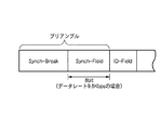
図1は本発明にかかるデータ通信システムの構成例を示す概念図であり、相互に通信可能に接続された複数(図示の例では4つ)の送受信装置1-1、1-2、1-3、1-4のうちの一つの送受信装置1-1がマスタ装置100として機能し、他の装置がスレーブ装置200として各々機能するシステム構成例を示している。このデータ通信システムは、電力線通信(PLC(Power Line Communication))を用いたLIN(Local Interconnect Network)プロトコルによる車載通信システムの一部を成すものであり、車載機器に電力を供給するための電力線2を信号伝送路に利用して、車載機器を制御するためのデータ通信を行う。LINプロトコルによる通信では、フレームのヘッダ(ID- Field)の前に、プリアンブルとしてシンクフィールド(Synch-Field)およびシンクブレイク(Synch-Break)が送信される(図2参照)。
FIG. 1 is a conceptual diagram showing a configuration example of a data communication system according to the present invention, and a plurality of (four in the illustrated example) transmission / reception devices 1-1, 1-2, 1- connected to be communicable with each other. 3 shows an example of a system configuration in which one transmission / reception device 1-1 of 1-4 is functioning as the
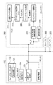
図3は本発明にかかるデータ通信システムにおけるマスタ装置とスレーブ装置の構成例を示すブロック図である。 FIG. 3 is a block diagram showing a configuration example of a master device and a slave device in the data communication system according to the present invention.
マスタ装置100は、水晶発振子101を内蔵したメインクロック生成部102を備えている。メインクロック生成部102は、水晶発振子101の発信信号をメインクロック信号CLK_M(周波数fm)として出力する。メインクロック信号CLK_Mは、データレート設定部104に入力される。データレート設定部104は、メインクロック信号CLK_Mを定数Cに応じて分周することにより送信データの伝送レートを設定する。その設定値は送信データ生成部105に入力される。送信データ生成部105は、設定された伝送レートで送信データTX_Mを生成する。送信データTX_Mは電力線2に送出される。
The
一方、電力線2を介してスレーブ装置200から送られてきた信号は信号処理部109に入力され信号処理される。
On the other hand, a signal transmitted from the
スレーブ装置200は、可変容量ダイオードを用いたRC発振回路またはLC発振回路からなるVCOをメインクロック生成部209として備えている。スレーブ装置200では、電力線2を介して送られてきた信号Rx_Sが信号処理部203およびMMC周波数情報検出部230に入力される。信号処理部203は受信信号Rx_Sを処理する。尚、『MMC』とは『マスタ装置に搭載のメインクロック』の略称である。
The
MMC周波数情報検出部230は、マスタ装置100からの受信信号Rx_Sに含まれるプリアンブル信号に基づいて当該受信信号Rx_Sの中のマスタ装置100側のメインクロック周波数情報を読み取る。ここで読み取られたメインクロック周波数情報はメインクロック調整部231に渡される。
The MMC frequency
メインクロック調整部231は、マスタ装置100側のメインクロック周波数情報を元に、スレーブ装置200のメインクロック周波数fsをマスタ装置100と同じ周波数fmに調整するための調整信号を生成する。生成された調整信号はメインクロック生成部209に送られる。
The main
メインクロック生成部209は、自スレーブ装置200のメインクロック周波数をメインクロック調整部231からの調整信号に合わせて調整しつつ、メインクロック信号CLK_S(fs)を生成する。生成されたメインクロック信号CLK_S(fs)はデータレート設定部210に送られる。
The main
データレート設定部210は、メインクロック生成部209によって生成されるメインクロック信号CLK_S(fs)を定数Cに応じて分周することにより送信データTX_Sの伝送レートを設定する。その設定値は送信データ生成部212に渡される。
The data
送信データ生成部212は、データレート設定部210で設定された伝送レートで送信データTX_Sを生成する。送信データTX_Sは電力線2を介してマスタ装置100に送られる。
The transmission
図4は本発明にかかるデータ通信システムにおけるマスタ装置とスレーブ装置の別の構成例を示すブロック図である。 FIG. 4 is a block diagram showing another configuration example of the master device and the slave device in the data communication system according to the present invention.
マスタ装置100は、水晶発振子101を内蔵したメインクロック生成部102を備えている。メインクロック生成部102は、水晶発振子101の発信信号をメインクロック信号CLK_M(周波数fm)として出力する。メインクロック信号CLK_Mは、データレート設定部104とキャリア信号生成部103とに入力される。データレート設定部104は、メインクロック信号CLK_Mを定数Cに応じて分周することにより送信データの伝送レートを設定する。その設定値は送信データ生成部105に入力される。
The
キャリア信号生成部103は、メインクロック生成部101によって生成されるメインクロック信号CLK_Mを信号処理してキャリア信号C_Mを生成する。送信データ生成部105は、データレート設定部104にて設定された伝送レートで送信データTx_Mを生成する。送信データTX_M及びキャリア信号C_Mは、変調部106に送られる。
The carrier
変調部106は、キャリア信号C_Mを送信データTx_Mに応じて変調する。変調部106の出力信号は帯域フィルタ107を通して電力線2に送出される。
The
一方、電力線2を介してスレーブ装置200から送られてきた信号は、帯域フィルタ107を通して復調部108に入力される。復調部108で復調された受信信号は、信号処理部109に入力され信号処理される。
On the other hand, a signal transmitted from the
スレーブ装置200は、可変容量ダイオードを用いたRC発振回路またはLC発振回路からなるVCOをメインクロック生成部209として備えている。スレーブ装置200では、電力線2を介して送られてきた信号が、帯域フィルタ201を通して復調部202に入力される。復調部202は、受信信号Rxを復調する(図7参照)。復調された受信信号Rx_Sは、信号処理部203およびMMC周波数情報検出部230に入力される。信号処理部203は受信信号Rx_Sを処理する。
The
MMC周波数情報検出部230は、マスタ装置100からの受信信号Rx_Sに含まれるプリアンブル信号に基づいて当該受信信号Rx_Sの中のマスタ装置100側のメインクロック周波数情報を読み取り、その情報をメインクロック調整部231に渡す。
The MMC frequency
メインクロック調整部231は、マスタ装置100側のメインクロック周波数情報を元に、自装置のメインクロック周波数をマスタ装置100と同じ周波数に調整するための調整信号を生成する。生成された調整信号はメインクロック生成部209に送られる。
The main
メインクロック生成部209は、自スレーブ装置200のメインクロック周波数fsをメインクロック調整部231からの調整信号に合わせて調整しつつ、メインクロック信号CLK_Sを生成する。生成されたメインクロック信号CLK_Sはデータレート設定部210とキャリア信号生成部211とに送られる。
The main
データレート設定部210は、メインクロック生成部209によって生成されるメインクロック信号CLK_Sを定数Cに応じて分周することにより送信データTX_Sの伝送レートを設定する。その設定値は送信データ生成部212に渡される。送信データ生成部212は、データレート設定部210で設定された伝送レートで送信データTX_Sを生成する。キャリア信号生成部211は、メインクロック生成部209によって生成されるメインクロック信号CLK_Sを信号処理してキャリア信号C_Sを生成する。送信データTX_Sおよびキャリア信号C_Sは変調部213に送られる。
The data
変調部213は、キャリア信号C_Mを送信データTx_Mに応じて変調する。変調部213の出力信号は帯域フィルタ201を通して電力線2に送出される。
The
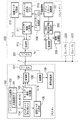
図5は本発明にかかるデータ通信システムにおけるマスタ装置とスレーブ装置のさらに別の構成例を示すブロック図である。 FIG. 5 is a block diagram showing still another configuration example of the master device and the slave device in the data communication system according to the present invention.
マスタ装置100は、水晶発振子101を内蔵したメインクロック生成部102を備えている。メインクロック生成部102は、水晶発振子101の発信信号をメインクロック信号CLK_M(周波数fm)として出力する。メインクロック信号CLK_Mは、キャリア信号生成部103とデータレート設定部104とに入力される。キャリア信号生成部103は、メインクロック信号CLK_Mを分周することにより所定周波数fcのキャリア信号C_Mを生成する。
The
データレート設定部104は、メインクロック信号CLK_Mを定数Cで分周する。その設定値は送信データ生成部105に入力される。
The data
変調部106は、キャリア信号C_Mを送信データTx_Mに応じて変調する。変調部106の出力信号は帯域フィルタ107を通して電力線2に送出される。
The
一方、電力線2を介してスレーブ装置200から送られてきた信号は、帯域フィルタ107を通して復調部108に入力される。復調部108で復調された受信信号は、信号処理部109に入力され処理される。
On the other hand, a signal transmitted from the
スレーブ装置200は、可変容量ダイオードを用いたRC発振回路またはLC発振回路からなるVCOをメインクロック生成部209として備えている。スレーブ装置200では、電力線2を介して送られてきた信号が、帯域フィルタ201を通して復調部202に入力される。復調部202は、受信信号Rxを復調する(図7参照)。復調された受信信号Rx_Sは、信号処理部203、位相差検出部205、および信号検出部206に入力される。信号処理部203は受信信号Rx_Sを処理する。
The
位相差検出部205には、復調された受信信号Rx_Sとともに分周部207からの出力信号S0が入力される。位相差検出部205は、受信信号Rx_Sと分周部207からの出力信号S0との位相差に比例した電圧の信号(位相差信号)を出力する。位相差信号は、メインクロック調整部208に入力される。
The
信号検出部206は、復調された受信信号Rx_S中のシンクフィールドを解析することにより、マスタ装置100からの受信信号の有無を検出する。マスタ装置100からの受信信号有りと検出したら、その旨を示すマスタ信号検知信号をメインクロック調整部208に出力する。メインクロック調整部208は、マスタ信号検知信号が入力されない時は、位相差検出部205からの位相差信号をホールドして出力し続ける。その位相差信号がメインクロック生成部209に入力される。
The
メインクロック生成部209は、位相差信号の電圧に応じた周波数fsのクロック信号CLK_Sを出力する。クロック生成部209から出力されたクロック信号CLK_Sは、分周部207とデータレート設定部210とキャリア信号生成部211とに入力される。
The main
分周部207は、クロック生成部209からの周波数fsのクロック信号CLK_Sを定数Cで分周した出力信号S0を出力する。
The
上記のように、メインクロック生成部209により生成されたクロック信号CLK_Sを、分周部207によって定数Cで分周し、その出力信号S0を位相差検出部205にフィードバックさせることにより、クロック生成部207により生成されるクロック信号CLK_Sの周波数fsがマスタ装置100のメインクロック生成部102により生成されるクロック信号CLK_Mの周波数fmと一致するように調整される。
As described above, the clock signal CLK_S generated by the main
データレート設定部210は、メインクロック生成部209により生成されたクロック信号CLK_Sを定数Cに応じて分周することによって、送信データレートを設定する。その設定値は送信データ生成部212に入力される。送信データ生成部212は、送信データTx_Sを生成する。キャリア信号生成部211は、クロック信号CLK_Sを分周することにより所定周波数fcs(=fcm)のキャリア信号C_Sを生成する。キャリア信号C_Sおよび送信データTx_Sは変調部213に送られる。変調部213は、キャリア信号C_Sを送信データTx_Sに応じて変調する。変調部213の出力信号は帯域フィルタ201を通して電力線2に送出される。
The data
スレーブ装置200は、マスタ装置100から受信信号Rx_S中のプリアンブル等の信号に基づいて伝送データレートを検出し、自装置のクロック生成部209で生成したクロック信号CLK_Sを伝送データレートに応じて分周し、マスタ装置100の送信用キャリア信号C_Mと分周部207の出力信号との位相差に応じた電圧の信号を自装置のクロック生成部209に入力することにより、自装置のクロック生成部209の発振周波数fsをマスタ装置100のメインクロック発生部102の発振周波数fmと一致させる。
The
したがって、各スレーブ装置200のメインクロック生成部209にRC発振回路やLC発振回路といった安価なものを使用しつつ、各スレーブ装置200のクロック信号CLK_Sを、高価な水晶振動子101を備えたマスタ装置100のメインクロック信号CLK_Mと一致させることができるので、全ての送受信装置に水晶振動子101を搭載した場合と同等に伝送品質の高いデータ通信システムを安価に実現できる。
Therefore, the master device including the
図8は本発明にかかるデータ通信システムにおけるマスタ装置とスレーブ装置の別の構成例を示すブロック図である。図5に示したデータ通信システムとの違いはスレーブ装置200の構成にある。 FIG. 8 is a block diagram showing another configuration example of the master device and the slave device in the data communication system according to the present invention. The difference from the data communication system shown in FIG.
図8に示すデータ通信システムのスレーブ装置200では、復調部202で復調された受信信号Rx_Sが、信号処理部220とビット幅検出部221とに入力される。信号処理部220は受信信号Rx_Sを処理する。
In the
ビット幅検出部221は、マスタ装置100からの受信信号Rx_S中の信号の立ち上がりと立ち下がりの間の時間をカウントすることにより受信信号Rx_Sの1ビット幅を検出する。ビット幅検出部221による検出値はビット幅比較部223に入力される。このときビット幅比較部223には、基準ビット幅記憶部222から読み出された値も同時に入力される。基準ビット幅記憶部222は、基準となる1ビット幅の値を予め記憶している。
The bit
ビット幅比較部223は、入力された両値を比較し、両値の差分に応じた信号を出力する。ビット幅比較部223の出力信号はメインクロック信号調整部224に入力される。メインクロック信号調整部224は、ビット幅比較部223からの信号に基づいて、前記差分を無くすようにメインクロック生成部209への入力信号電圧を調整する。メインクロック生成部209の動作および、メインクロック生成部209のクロック信号CLK_Sを用いるデータレート設定部210、キャリア信号生成部211、送信データ生成部212等の動作は図5の場合と同様である。
The bit
このように、図8のデータ通信システムは、各スレーブ装置200が、マスタ装置100からの受信信号Rx_Sに含まれる信号に基づいて受信信号Rx_Sの1ビット幅を検出し、その1ビット幅と予め記憶しておいた基準ビット幅との差分を無くすように自装置のクロック生成部209への入力信号電圧を調整する。これにより、自装置のクロック信号CLK_Sとマスタ装置100のクロック信号CLK_Sとのずれが抑制される。
As described above, in the data communication system of FIG. 8, each
各スレーブ装置200のメインクロック信号調整処理は、実際の負荷制御等を行うデータ通信中に順次、調整を行うことが可能である。
The main clock signal adjustment processing of each
図8のデータ通信システムの場合も、各スレーブ装置200のクロック生成部209にRC発振回路やLC発振回路といった安価なものを使用しつつ、各スレーブ装置200のクロック信号CLK_Sを、高価な水晶振動子101を備えたマスタ装置100のメインクロック信号CLK_Mと一致させることができるので、全ての送受信装置に水晶振動子101を搭載した場合と同等に伝送品質の高いデータ通信システムを安価に実現できる。
Also in the case of the data communication system of FIG. 8, the clock signal CLK_S of each
尚、本発明は、前述した形態例に限定されるものではなく、適宜、変形、改良、等が可能である。その他、前述した形態例における各構成要素の形態、数、配置箇所、等は本発明を達成できるものであれば任意であり、限定されない。 The present invention is not limited to the above-described embodiments, and modifications, improvements, etc. can be made as appropriate. In addition, the configuration, the number, the arrangement location, and the like of each component in the above-described embodiment are arbitrary and are not limited as long as the present invention can be achieved.
上記の実施形態例では、PLCによるデータ通信システムを例にとり説明したが、専用の伝送線を用いたデータ通信システムにも本発明が適用できることはいうまでもない。また、使用する通信プロトコルもLINに限定されない。 In the above embodiment, the data communication system using the PLC has been described as an example. However, it goes without saying that the present invention can also be applied to a data communication system using a dedicated transmission line. Further, the communication protocol to be used is not limited to LIN.
1-1、1-2、1-3、1-4 送受信装置
2 電力線
100 マスタ装置
200 スレーブ装置
101 水晶発振子
102 メインクロック生成部
103 キャリア信号生成部
104 データレート設定部
105 送信データ生成部
202 復調部
203 信号処理部
204 データレート計測部
205 位相差検出部
206 信号検出部
207 分周部
208 メインクロック調整部
209 メインクロック生成部
212 送信データ生成部
220 信号処理部
221 ビット幅検出部
222 基準ビット幅記憶部
224 メインクロック信号調整部
223 ビット幅比較部
230 MMC周波数情報検出部
231 メインクロック調整部
CLK_M メインクロック信号
CLK_S クロック信号
C_M キャリア信号
C_S キャリア信号
Rx_S 受信信号
Tx_M 送信データ
Tx_S 送信データ
1-1, 1-2, 1-3, 1-4 Transmission /
Claims (4)
マスタ側の送受信装置は、
周波数確度の高いメインクロック信号を生成するメインクロック生成部と、
前記メインクロック生成部によって生成されるメインクロック信号を定数Cに応じて分周することにより送信データの伝送レートを設定するデータレート設定部と、
前記データレート設定部で設定された伝送レートでデータを生成する送信データ生成部と、
受信信号を受信し処理する信号処理部と、を持ち、
複数のスレーブ側の受信装置は、
受信信号を受信し信号処理する信号処理部と、
マスタ側の送受信装置からの受信信号に含まれるプリアンブル等の信号に基づいて当該受信信号の中のマスタ側のメインクロック周波数情報を読み取るMMC周波数情報検出部と、
マスタ側のメインクロック周波数情報を元に、自送受信装置のメインクロック周波数をマスタと同じ周波数に調整するための調整信号を生成するメインクロック調整部と、
自送受信装置のメインクロック周波数を前記メインクロック調整部からの調整信号に合わせて調整可能な、マスタ側のメインクロック生成部よりも周波数確度及び周波数安定度の低いメインクロック生成部と、
自送受信装置の前記クロック生成部によって生成されるメインクロック信号を定数Cに応じて分周することにより送信データの伝送レートを設定するデータレート設定部と、
前記データレート設定部で設定された伝送レートで送信データを生成する送信データ生成部と、
を有することを特徴とするデータ通信システム。 In a data communication system in which a master-side transceiver device and a plurality of slave-side transceiver devices communicate bidirectionally,
The transmitting / receiving device on the master side
A main clock generator for generating a main clock signal with high frequency accuracy;
A data rate setting unit that sets a transmission rate of transmission data by dividing the main clock signal generated by the main clock generation unit according to a constant C;
A transmission data generation unit that generates data at a transmission rate set by the data rate setting unit;
A signal processing unit that receives and processes received signals;
Multiple slave side receivers
A signal processing unit for receiving and processing a received signal;
An MMC frequency information detection unit that reads main clock frequency information on the master side in the received signal based on a signal such as a preamble included in the received signal from the transmission / reception device on the master side;
Based on main clock frequency information on the master side, a main clock adjustment unit that generates an adjustment signal for adjusting the main clock frequency of the own transceiver device to the same frequency as the master,
A main clock generator having a lower frequency accuracy and frequency stability than the main clock generator on the master side, which can adjust the main clock frequency of the own transceiver device according to the adjustment signal from the main clock adjuster,
A data rate setting unit that sets a transmission rate of transmission data by dividing the main clock signal generated by the clock generation unit of the own transmission / reception device according to a constant C;
A transmission data generation unit that generates transmission data at a transmission rate set by the data rate setting unit;
A data communication system comprising:
マスタ側の送受信装置は、
周波数確度の高いメインクロック信号を生成するメインクロック生成部と、
前記メインクロック生成部によって生成されるメインクロック信号を定数Cに応じて分周することにより送信データの伝送レートを設定するデータレート設定部と、
前記データレート設定部で設定された伝送レートでデータを生成する送信データ生成部と、
前記メインクロック生成部によって生成されるメインクロック信号を信号処理してキャリア信号を生成するキャリア信号生成部と、
前記送信データ生成部及び前記キャリア信号生成部で生成された信号を変調する変調部と、
変調された受信信号を復調する復調部と、
復調された受信信号を信号処理する信号処理部と、を持ち、
複数のスレーブ側の受信装置は、
変調された受信信号を復調する復調部と、
復調された受信信号を信号処理する信号処理部と、
プリアンブル信号を含むマスタ側の送受信装置からの受信信号に基づいて当該受信信号の中のマスタ側のメインクロック周波数情報を読み取るMMC周波数情報検出部と、
マスタ側のメインクロック周波数情報を元に、自送受信装置のメインクロック周波数をマスタと同じ周波数に調整するための調整信号を生成するメインクロック調整部と、
自送受信装置のメインクロック周波数を前記メインクロック調整部からの調整信号に合わせて調整可能な、マスタ側のメインクロック生成部よりも周波数確度及び周波数安定度の低いメインクロック生成部と、
自送受信装置の前記クロック生成部によって生成されるクロック信号を定数Cに応じて分周することにより送信データの伝送レートを設定するデータレート設定部と、
前記データレート設定部で設定された伝送レートで送信データを生成する送信データ生成部と、
自送受信装置の前記メインクロック生成部によって生成されるメインクロック信号を信号処理してキャリア信号を生成するキャリア信号生成部と、
前記送信データ生成部及び前記キャリア信号生成部で生成された信号を変調する変調部と、
を有することを特徴とするデータ通信システム。 In a data communication system in which a master-side transmitting / receiving device and a plurality of slave-side transmitting / receiving devices perform modulation / demodulation using a single carrier signal and perform bidirectional communication,
The transmitting / receiving device on the master side
A main clock generator for generating a main clock signal with high frequency accuracy;
A data rate setting unit that sets a transmission rate of transmission data by dividing the main clock signal generated by the main clock generation unit according to a constant C;
A transmission data generation unit that generates data at a transmission rate set by the data rate setting unit;
A carrier signal generation unit that generates a carrier signal by performing signal processing on the main clock signal generated by the main clock generation unit;
A modulation unit that modulates signals generated by the transmission data generation unit and the carrier signal generation unit;
A demodulator that demodulates the modulated received signal;
A signal processing unit that performs signal processing on the demodulated received signal;
Multiple slave side receivers
A demodulator that demodulates the modulated received signal;
A signal processing unit that processes the demodulated received signal;
An MMC frequency information detector that reads main clock frequency information on the master side in the received signal based on the received signal from the transmitting / receiving device on the master side including the preamble signal;
Based on main clock frequency information on the master side, a main clock adjustment unit that generates an adjustment signal for adjusting the main clock frequency of the own transceiver device to the same frequency as the master,
A main clock generator having a lower frequency accuracy and frequency stability than the main clock generator on the master side, which can adjust the main clock frequency of the own transceiver device according to the adjustment signal from the main clock adjuster,
A data rate setting unit that sets a transmission rate of transmission data by dividing the clock signal generated by the clock generation unit of the own transmission / reception device according to a constant C;
A transmission data generation unit that generates transmission data at a transmission rate set by the data rate setting unit;
A carrier signal generation unit that generates a carrier signal by performing signal processing on the main clock signal generated by the main clock generation unit of the own transceiver device;
A modulation unit that modulates signals generated by the transmission data generation unit and the carrier signal generation unit;
A data communication system comprising:
マスタ側の送受信装置は、
周波数確度の高いメインクロック信号を生成するメインクロック生成部と、
前記メインクロック生成部によって生成されるメインクロック信号を定数Cに応じて分周することにより送信データの伝送レートを設定するデータレート設定部と、
前記データレート設定部で設定された伝送レートで送信データを生成する送信データ生成部と、
前記メインクロック生成部によって生成されるメインクロック信号を信号処理してキャリア信号を生成するキャリア信号生成部と、
前記送信データ生成部及び前記キャリア信号生成部で生成された信号を変調する変調部と、
変調された受信信号を復調する復調部と、
復調された受信信号を信号処理する信号処理部と、を持ち、
複数のスレーブ側の受信装置は、
変調された受信信号を復調する復調部と、
復調された受信信号を信号処理する信号処理部と、
自送受信装置のメインクロック生成部で生成されたメインクロック信号を定数Cに応じて分周する分周部と、
マスタ側の送受信装置からの受信信号と前記分周部の出力信号との位相差に応じた電圧信号を出力する位相差検出部と、
マスタ側の送受信装置からの受信信号の中から前記位相差検出部が検出可能な信号か検出不可能な信号かを読み取る信号検出部と、
前記位相差検出部から出力された電圧信号と前記信号検出部からの出力信号を元に、自送受信装置のメインクロック周波数をマスタと同じ周波数に調整するための調整信号を生成するメインクロック調整部と、
自送受信装置のメインクロック周波数を前記メインクロック調整部からの調整信号に合わせて調整可能な、マスタ側のメインクロック生成部よりも周波数確度及び周波数安定度の低いメインクロック生成部と、
前記メインクロック生成部によって生成されるメインクロック周波数を定数Cに応じて分周することにより送信データの伝送レートを設定するデータレート設定部と、
前記データレート設定部で設定された伝送レートで送信データを生成する送信データ生成部と、
自送受信装置の前記メインクロック生成部によって生成されるメインクロック信号を信号処理してキャリア信号を生成するキャリア信号生成部と、
前記送信データ生成部及び前記キャリア信号生成部で生成された信号を変調する変調部と、
を有することを特徴とするデータ通信システム。 In a data communication system in which a master-side transmitting / receiving device and a plurality of slave-side transmitting / receiving devices perform modulation / demodulation using a single carrier signal and perform bidirectional communication,
The transmitting / receiving device on the master side
A main clock generator for generating a main clock signal with high frequency accuracy;
A data rate setting unit that sets a transmission rate of transmission data by dividing the main clock signal generated by the main clock generation unit according to a constant C;
A transmission data generation unit that generates transmission data at a transmission rate set by the data rate setting unit;
A carrier signal generation unit that generates a carrier signal by performing signal processing on the main clock signal generated by the main clock generation unit;
A modulation unit that modulates signals generated by the transmission data generation unit and the carrier signal generation unit;
A demodulator that demodulates the modulated received signal;
A signal processing unit that performs signal processing on the demodulated received signal;
Multiple slave side receivers
A demodulator that demodulates the modulated received signal;
A signal processing unit that processes the demodulated received signal;
A frequency dividing unit that divides the main clock signal generated by the main clock generating unit of the own transmission / reception device according to a constant C;
A phase difference detection unit that outputs a voltage signal corresponding to a phase difference between a reception signal from a transmission / reception device on the master side and an output signal of the frequency division unit;
A signal detection unit that reads whether the phase difference detection unit is a detectable signal or a non-detectable signal from the reception signals from the master side transmission / reception device;
Based on the voltage signal output from the phase difference detection unit and the output signal from the signal detection unit, a main clock adjustment unit that generates an adjustment signal for adjusting the main clock frequency of the own transmission / reception device to the same frequency as the master When,
A main clock generator having a lower frequency accuracy and frequency stability than the main clock generator on the master side, which can adjust the main clock frequency of the own transceiver device according to the adjustment signal from the main clock adjuster,
A data rate setting unit that sets a transmission rate of transmission data by dividing the main clock frequency generated by the main clock generation unit according to a constant C;
A transmission data generation unit that generates transmission data at a transmission rate set by the data rate setting unit;
A carrier signal generation unit that generates a carrier signal by performing signal processing on the main clock signal generated by the main clock generation unit of the own transceiver device;
A modulation unit that modulates signals generated by the transmission data generation unit and the carrier signal generation unit;
A data communication system comprising:
マスタの送受信装置は、
周波数確度の高いメインクロック信号を生成するメインクロック生成部と、
前記メインクロック生成部によって生成されるメインクロック信号を定数Cに応じて分周することにより送信データの伝送レートを設定するデータレート設定部と、
前記データレート設定部で設定された伝送レートで送信データを生成する送信データ生成部と、
前記メインクロック生成部によって生成されるメインクロック信号を信号処理してキャリア信号を生成するキャリア信号生成部と、
前記送信データ生成部及び前記キャリア信号生成部で生成された信号を変調する変調部と、
変調された受信信号を復調する復調部と、
復調された受信信号を信号処理する信号処理部と、を持ち、
複数のスレーブ側の受信装置は、
変調された受信信号を復調する復調部と、
復調された受信信号を信号処理する信号処理部と、
マスタ側の送受信装置からの受信信号に含まれるプリアンブル等の信号に基づいて当該受信信号の1ビットの時間幅を検出するビット幅検出部と、
自送受信装置のメインクロック周波数がマスタ側の送受信装置と同じ周波数の場合に前記ビット幅検出部から出力される信号の1ビットの時間幅を記憶しておく基準ビット幅記憶部と、
前記ビット幅検出部により検出された時間幅と前記基準ビット幅記憶部に記憶されている時間幅とを比較するビット幅比較部と、
前記ビット幅比較部から出力された信号に基づいて、自送受信装置のメインクロック周波数をマスタと同じ周波数に調整するための調整信号を生成するメインクロック調整部と、
自送受信装置のメインクロック周波数を前記メインクロック調整部からの調整信号に合わせて調整可能な、マスタ側のメインクロック生成部よりも周波数確度及び周波数安定度の低いメインクロック生成部と、
前記メインクロック生成部によって生成されるメインクロック周波数を定数Cに応じて分周することにより送信データの伝送レートを設定するデータレート設定部と、
前記データレート設定部で設定された伝送レートで送信データを生成する送信データ生成部と、
自送受信装置の前記メインクロック生成部によって生成されるメインクロック信号を信号処理してキャリア信号を生成するキャリア信号生成部と、
前記送信データ生成部及び前記キャリア信号生成部で生成された信号を変調する変調部と、
を有することを特徴とするデータ通信システム。 In a data communication system in which a master-side transmitting / receiving device and a plurality of slave-side transmitting / receiving devices perform modulation / demodulation using a single carrier signal and perform bidirectional communication,
The master transceiver is
A main clock generator for generating a main clock signal with high frequency accuracy;
A data rate setting unit that sets a transmission rate of transmission data by dividing the main clock signal generated by the main clock generation unit according to a constant C;
A transmission data generation unit that generates transmission data at a transmission rate set by the data rate setting unit;
A carrier signal generation unit that generates a carrier signal by performing signal processing on the main clock signal generated by the main clock generation unit;
A modulation unit that modulates signals generated by the transmission data generation unit and the carrier signal generation unit;
A demodulator that demodulates the modulated received signal;
A signal processing unit that performs signal processing on the demodulated received signal;
Multiple slave side receivers
A demodulator that demodulates the modulated received signal;
A signal processing unit that processes the demodulated received signal;
A bit width detector that detects a 1-bit time width of the received signal based on a signal such as a preamble included in the received signal from the master-side transmitting / receiving device;
A reference bit width storage unit that stores a 1-bit time width of a signal output from the bit width detection unit when the main clock frequency of the own transmission / reception device is the same frequency as the master side transmission / reception device;
A bit width comparison unit that compares the time width detected by the bit width detection unit with the time width stored in the reference bit width storage unit;
Based on the signal output from the bit width comparison unit, a main clock adjustment unit that generates an adjustment signal for adjusting the main clock frequency of the own transmission / reception device to the same frequency as the master,
A main clock generator having a lower frequency accuracy and frequency stability than the main clock generator on the master side, which can adjust the main clock frequency of the own transceiver device according to the adjustment signal from the main clock adjuster,
A data rate setting unit that sets a transmission rate of transmission data by dividing the main clock frequency generated by the main clock generation unit according to a constant C;
A transmission data generation unit that generates transmission data at a transmission rate set by the data rate setting unit;
A carrier signal generation unit that generates a carrier signal by performing signal processing on the main clock signal generated by the main clock generation unit of the own transceiver device;
A modulation unit that modulates signals generated by the transmission data generation unit and the carrier signal generation unit;
A data communication system comprising:
Priority Applications (1)
| Application Number | Priority Date | Filing Date | Title |
|---|---|---|---|
| JP2004115889A JP2005303631A (en) | 2004-04-09 | 2004-04-09 | Data communications system |
Applications Claiming Priority (1)
| Application Number | Priority Date | Filing Date | Title |
|---|---|---|---|
| JP2004115889A JP2005303631A (en) | 2004-04-09 | 2004-04-09 | Data communications system |
Publications (1)
| Publication Number | Publication Date |
|---|---|
| JP2005303631A true JP2005303631A (en) | 2005-10-27 |
Family
ID=35334646
Family Applications (1)
| Application Number | Title | Priority Date | Filing Date |
|---|---|---|---|
| JP2004115889A Abandoned JP2005303631A (en) | 2004-04-09 | 2004-04-09 | Data communications system |
Country Status (1)
| Country | Link |
|---|---|
| JP (1) | JP2005303631A (en) |
Cited By (4)
| Publication number | Priority date | Publication date | Assignee | Title |
|---|---|---|---|---|
| WO2007125579A1 (en) * | 2006-04-27 | 2007-11-08 | Mitsubishi Denki Kabushiki Kaisha | Receiver, communication apparatus and communication system |
| US7631212B2 (en) * | 2006-04-03 | 2009-12-08 | Denso Corporation | Communication system, communication device and method for determining duty ratio of PWM control |
| JP2016122901A (en) * | 2014-12-24 | 2016-07-07 | 国立大学法人東北大学 | Receiving data restoration device |
| JP2018067877A (en) * | 2016-10-21 | 2018-04-26 | シャープ株式会社 | Data transceiver |
-
2004
- 2004-04-09 JP JP2004115889A patent/JP2005303631A/en not_active Abandoned
Cited By (7)
| Publication number | Priority date | Publication date | Assignee | Title |
|---|---|---|---|---|
| US7631212B2 (en) * | 2006-04-03 | 2009-12-08 | Denso Corporation | Communication system, communication device and method for determining duty ratio of PWM control |
| US7982512B2 (en) | 2006-04-03 | 2011-07-19 | Denso Corporation | Communication system communication device and method for determining duty ratio of PWM control |
| WO2007125579A1 (en) * | 2006-04-27 | 2007-11-08 | Mitsubishi Denki Kabushiki Kaisha | Receiver, communication apparatus and communication system |
| JPWO2007125579A1 (en) * | 2006-04-27 | 2009-09-10 | 三菱電機株式会社 | Receiver, communication apparatus and communication system |
| JP4653839B2 (en) * | 2006-04-27 | 2011-03-16 | 三菱電機株式会社 | Receiver, communication apparatus and communication system |
| JP2016122901A (en) * | 2014-12-24 | 2016-07-07 | 国立大学法人東北大学 | Receiving data restoration device |
| JP2018067877A (en) * | 2016-10-21 | 2018-04-26 | シャープ株式会社 | Data transceiver |
Similar Documents
| Publication | Publication Date | Title |
|---|---|---|
| TWI492019B (en) | Electronic apparatus and clock generating method thereof | |
| JPH10322259A (en) | Digital cordless communication system | |
| US6078578A (en) | Communication apparatus | |
| US7502435B2 (en) | Two-point modulator arrangement and use thereof in a transmission arrangement and in a reception arrangement | |
| US20070014339A1 (en) | Data communication system | |
| JP2005303631A (en) | Data communications system | |
| JP2001251210A (en) | Mutual frequency lock between both ends of link | |
| JP2005303632A (en) | Data communications system | |
| JP2007089032A (en) | Receiver and radio communication device | |
| EP0949758B1 (en) | Communications system, mobile device and method | |
| US20060023796A1 (en) | ASK communication device | |
| EP1521369A1 (en) | Clock signal correcting circuit and communicating apparatus | |
| US6546060B1 (en) | Direct modulating FSK transmitter for MCA | |
| JP2006211143A (en) | Clock and data reproducing circuit | |
| JP2005252355A (en) | Clock shaping device | |
| JP2010109831A (en) | System and method for controlling pll transient response | |
| KR950002444B1 (en) | Data clock demodulating circuit of auto-vehicle pursuiting device | |
| JP2009218863A (en) | Oscillator, its oscillation method, transmitter its transmission method, receiver, and its receiving method | |
| JP4459469B2 (en) | Automatic frequency controller | |
| JP2636614B2 (en) | Double superheterodyne radio | |
| JP4319110B2 (en) | Wireless communication device | |
| KR0145863B1 (en) | Frequency synthesizer in spread spectrum system | |
| JPH09326752A (en) | Mobile communication terminal equipment | |
| JPS62120735A (en) | Method and apparatus for frequency hopping spread spectrum power line carrier communication | |
| JPH0831888B2 (en) | Wireless communication device |
Legal Events
| Date | Code | Title | Description |
|---|---|---|---|
| RD04 | Notification of resignation of power of attorney |
Free format text: JAPANESE INTERMEDIATE CODE: A7424 Effective date: 20060327 |
|
| A621 | Written request for application examination |
Free format text: JAPANESE INTERMEDIATE CODE: A621 Effective date: 20070328 |
|
| RD04 | Notification of resignation of power of attorney |
Free format text: JAPANESE INTERMEDIATE CODE: A7424 Effective date: 20071129 |
|
| A762 | Written abandonment of application |
Free format text: JAPANESE INTERMEDIATE CODE: A762 Effective date: 20090205 |