JP2005298917A - Non-conductive deposition method - Google Patents
Non-conductive deposition method Download PDFInfo
- Publication number
- JP2005298917A JP2005298917A JP2004117998A JP2004117998A JP2005298917A JP 2005298917 A JP2005298917 A JP 2005298917A JP 2004117998 A JP2004117998 A JP 2004117998A JP 2004117998 A JP2004117998 A JP 2004117998A JP 2005298917 A JP2005298917 A JP 2005298917A
- Authority
- JP
- Japan
- Prior art keywords
- resin
- part acrylic
- tin
- thin film
- forming
- Prior art date
- Legal status (The legal status is an assumption and is not a legal conclusion. Google has not performed a legal analysis and makes no representation as to the accuracy of the status listed.)
- Pending
Links
- 238000000151 deposition Methods 0.000 title claims description 11
- 239000011347 resin Substances 0.000 claims abstract description 127
- 229920005989 resin Polymers 0.000 claims abstract description 127
- 239000010410 layer Substances 0.000 claims abstract description 96
- ATJFFYVFTNAWJD-UHFFFAOYSA-N Tin Chemical compound [Sn] ATJFFYVFTNAWJD-UHFFFAOYSA-N 0.000 claims abstract description 83
- 239000010409 thin film Substances 0.000 claims abstract description 73
- 238000000034 method Methods 0.000 claims abstract description 53
- 239000011247 coating layer Substances 0.000 claims abstract description 22
- 238000001771 vacuum deposition Methods 0.000 claims abstract description 15
- NIXOWILDQLNWCW-UHFFFAOYSA-N acrylic acid group Chemical group C(C=C)(=O)O NIXOWILDQLNWCW-UHFFFAOYSA-N 0.000 claims description 97
- XUIMIQQOPSSXEZ-UHFFFAOYSA-N Silicon Chemical compound [Si] XUIMIQQOPSSXEZ-UHFFFAOYSA-N 0.000 claims description 53
- 229910052710 silicon Inorganic materials 0.000 claims description 53
- 239000010703 silicon Substances 0.000 claims description 53
- 229920002803 thermoplastic polyurethane Polymers 0.000 claims description 45
- 239000010408 film Substances 0.000 claims description 28
- BZHJMEDXRYGGRV-UHFFFAOYSA-N Vinyl chloride Chemical compound ClC=C BZHJMEDXRYGGRV-UHFFFAOYSA-N 0.000 claims description 22
- 238000007740 vapor deposition Methods 0.000 claims description 22
- 238000012546 transfer Methods 0.000 claims description 20
- 239000000758 substrate Substances 0.000 claims description 19
- 238000004544 sputter deposition Methods 0.000 claims description 15
- 238000007733 ion plating Methods 0.000 claims description 14
- 239000011248 coating agent Substances 0.000 claims description 12
- 238000000576 coating method Methods 0.000 claims description 12
- 229910052751 metal Inorganic materials 0.000 claims description 12
- 239000002184 metal Substances 0.000 claims description 12
- 239000011521 glass Substances 0.000 claims description 10
- 238000004528 spin coating Methods 0.000 claims description 10
- 238000005507 spraying Methods 0.000 claims description 9
- 230000008021 deposition Effects 0.000 claims 1
- 239000000463 material Substances 0.000 abstract description 11
- JOYRKODLDBILNP-UHFFFAOYSA-N Ethyl urethane Chemical compound CCOC(N)=O JOYRKODLDBILNP-UHFFFAOYSA-N 0.000 abstract 1
- 239000007788 liquid Substances 0.000 description 24
- 230000004888 barrier function Effects 0.000 description 9
- 239000011241 protective layer Substances 0.000 description 7
- 238000007598 dipping method Methods 0.000 description 5
- 239000010985 leather Substances 0.000 description 4
- 229920000642 polymer Polymers 0.000 description 4
- 238000005034 decoration Methods 0.000 description 3
- 229920002457 flexible plastic Polymers 0.000 description 3
- TWNQGVIAIRXVLR-UHFFFAOYSA-N oxo(oxoalumanyloxy)alumane Chemical compound O=[Al]O[Al]=O TWNQGVIAIRXVLR-UHFFFAOYSA-N 0.000 description 3
- SIWVEOZUMHYXCS-UHFFFAOYSA-N oxo(oxoyttriooxy)yttrium Chemical compound O=[Y]O[Y]=O SIWVEOZUMHYXCS-UHFFFAOYSA-N 0.000 description 3
- 238000005299 abrasion Methods 0.000 description 2
- 239000002253 acid Substances 0.000 description 2
- 150000001875 compounds Chemical class 0.000 description 2
- 229910003437 indium oxide Inorganic materials 0.000 description 2
- PJXISJQVUVHSOJ-UHFFFAOYSA-N indium(iii) oxide Chemical compound [O-2].[O-2].[O-2].[In+3].[In+3] PJXISJQVUVHSOJ-UHFFFAOYSA-N 0.000 description 2
- 238000004519 manufacturing process Methods 0.000 description 2
- XOLBLPGZBRYERU-UHFFFAOYSA-N tin dioxide Chemical compound O=[Sn]=O XOLBLPGZBRYERU-UHFFFAOYSA-N 0.000 description 2
- 229910001887 tin oxide Inorganic materials 0.000 description 2
- 239000004925 Acrylic resin Substances 0.000 description 1
- 229920000178 Acrylic resin Polymers 0.000 description 1
- 230000015572 biosynthetic process Effects 0.000 description 1
- 239000004020 conductor Substances 0.000 description 1
- 238000007796 conventional method Methods 0.000 description 1
- -1 etc. by spraying Substances 0.000 description 1
- 229910052738 indium Inorganic materials 0.000 description 1
- APFVFJFRJDLVQX-UHFFFAOYSA-N indium atom Chemical compound [In] APFVFJFRJDLVQX-UHFFFAOYSA-N 0.000 description 1
- MRNHPUHPBOKKQT-UHFFFAOYSA-N indium;tin;hydrate Chemical compound O.[In].[Sn] MRNHPUHPBOKKQT-UHFFFAOYSA-N 0.000 description 1
- 150000002500 ions Chemical class 0.000 description 1
- 230000001678 irradiating effect Effects 0.000 description 1
- 238000010030 laminating Methods 0.000 description 1
- 238000007747 plating Methods 0.000 description 1
- 238000011160 research Methods 0.000 description 1
- 238000012360 testing method Methods 0.000 description 1
Images
Landscapes
- Physical Vapour Deposition (AREA)
Abstract
【課題】
一般的にこれらの金属性の薄膜は通電性のものであり、これを不通電、とすることは考慮されて無く、また、従来はトップコートはウレタン系樹脂を塗装されており、耐摩耗性や耐候性や密着性に課題を有している。
【解決手段】
本発明は、純度が99.99%以上の錫を用いてフィラメント式真空蒸着法等により膜厚を電子間力顕微鏡の測定で500オングストロング以下の錫薄膜1を形成し、形成した錫薄膜1が不通電であることを特徴としたもので、更に、基材Aに下塗り層2を形成し、下塗り層2に錫薄膜1を形成し、錫薄膜1にハードコート層31を形成したものであり、更には、錫薄膜の上面に中塗り層4を形成したものであり、加えて、錫薄膜1の上面に中塗り層4を形成し、中塗り層4の上面に加飾部5を形成し、加飾部5の上面に上塗り層6を形成したものである。
【選択図】
図1【Task】
In general, these metallic thin films are electrically conductive and are not considered to be de-energized. In addition, the top coat is conventionally coated with urethane-based resin, so it is wear resistant. And weather resistance and adhesion.
[Solution]
In the present invention, a tin thin film 1 having a thickness of 500 angstroms or less is formed by measuring with an electron force microscope using a filament type vacuum deposition method or the like using tin having a purity of 99.99% or more. The undercoat layer 2 is formed on the base material A, the tin thin film 1 is formed on the undercoat layer 2, and the hard coat layer 31 is formed on the tin thin film 1. In addition, the intermediate coating layer 4 is formed on the upper surface of the tin thin film. In addition, the intermediate coating layer 4 is formed on the upper surface of the tin thin film 1, and the decorative portion 5 is formed on the upper surface of the intermediate coating layer 4. The top coat layer 6 is formed on the upper surface of the decorative portion 5.
[Selection]
FIG.
Description
本発明は不通電の蒸着方法に関するものであり、更に詳細には、一般的に導電性である金属の錫を不通電の錫薄膜に蒸着する方法に関するものである。 The present invention relates to a non-conducting vapor deposition method, and more particularly to a method of depositing generally conductive metal tin on a non-conducting tin thin film.
一般的にこれらの金属性の薄膜は通電性のものであり、これを不通電、又は、無通電とする、つまり、電気抵抗値を無限大とすることは考慮されて無く、絶縁性の樹脂等の素材による薄膜を形成することのみが考慮されており、一方、錫薄膜を真空蒸着する技術も開発されているが通電性の被膜を形成するもので、不通電状態と成ることは考慮されていないものである。 In general, these metallic thin films are electrically conductive and are not energized or de-energized, that is, it is not considered that the electrical resistance value is infinite. Only the formation of a thin film made of a material such as the above is considered. On the other hand, a technique for vacuum-depositing a tin thin film has also been developed. It is not.
また、従来の技術ではトップコートはウレタン系樹脂を塗装されており、耐摩耗性や耐候性や密着性に課題を有している。 Further, in the conventional technique, the top coat is coated with a urethane resin, which has problems in wear resistance, weather resistance, and adhesion.
例えば、フレキシブルプラスチック支持体及び、前記支持体の表面上に、酸化アルミニウム、酸、スズ及び酸化イットリウムの群から選ばれる物質で形成された約50〜180Aの厚さを有するバリヤー層を含む高無色透明性のバリヤーフィルム、並びにその製法で、このバリヤー層層は真空蒸着により形成されるもの(特許文献1参照)や、高分子成形体基板上に形成された酸化インジウムを主体とする透明導電性薄膜層上に、比誘電率が2以上の誘電体層を形成し、該誘電体層上に紫外線硬化樹脂を塗布、硬化させてなる透明導電性積層体、および透明導電性薄膜層を接着する方法において、透明導電性薄膜層と紫外線硬化樹脂層の間に、比誘電率が2以上の誘電体層を形成せしめることを特徴とするもの(特許文献2参照)や、透明導電薄膜上に、高分子化合物からなる保護層を成膜し、保護層は、UV硬化性樹脂の硬化膜であることが好ましく、これにより短時間に膜を形成することができ、また、保護層は、透明導電薄膜の膜面に垂直方向の導電性に影響を及ぼすことのない極薄い膜厚の保護層を形成すればよく、1から1000nmの範囲の膜厚であることが好ましく、1から100nmの範囲の膜厚であることが更に好ましいもの(特許文献3参照)が開示されている。
然し乍ら、フレキシブルプラスチック支持体及び、前記支持体の表面上に、酸化アルミニウム、酸、スズ及び酸化イットリウムの群から選ばれる物質で形成された約50〜180Aの厚さを有するバリヤー層を含む高無色透明性のバリヤーフィルム、並びにその製法で、このバリヤー層層は真空蒸着により形成されるものでは、その構成に、酸化アルミニウム、酸化スズ及び酸化イットリウムの群から選ばれる物質で約50〜180Aの厚さを有するバリヤー層を形成してフレキシブルプラスチック支持体を高無色透明性のバリヤーフィルムに製造するものであり、酸化スズは用いられているものであるが、バリヤーフィルムを製造するものである。 However, a highly colorless support comprising a flexible plastic support and a barrier layer having a thickness of about 50 to 180 A formed of a material selected from the group consisting of aluminum oxide, acid, tin and yttrium oxide on the surface of the support. When the barrier layer is formed by vacuum vapor deposition in a transparent barrier film and its manufacturing method, the structure is made of a material selected from the group consisting of aluminum oxide, tin oxide and yttrium oxide and has a thickness of about 50 to 180A. A barrier layer having a thickness is formed to produce a flexible plastic support as a highly colorless and transparent barrier film. Although tin oxide is used, a barrier film is produced.
更に、高分子成形体基板上に形成された酸化インジウムを主体とする透明導電性薄膜層上に、比誘電率が2以上の誘電体層を形成し、該誘電体層上に紫外線硬化樹脂を塗布、硬化させてなる透明導電性積層体、および透明導電性薄膜層を接着する方法において、透明導電性薄膜層と紫外線硬化樹脂層の間に、比誘電率が2以上の誘電体層を形成せしめることを特徴とするものでは、インジウムとスズとの酸化物(ITO)層を備えているものの透明導電性薄膜層を形成するためのものである。 Further, a dielectric layer having a relative dielectric constant of 2 or more is formed on the transparent conductive thin film layer mainly composed of indium oxide formed on the polymer molded body substrate, and an ultraviolet curable resin is formed on the dielectric layer. Forming a dielectric layer having a relative dielectric constant of 2 or more between a transparent conductive thin film layer and an ultraviolet curable resin layer in a method of adhering a transparent conductive laminate and a transparent conductive thin film layer formed by coating and curing What is characterized is that the transparent conductive thin film layer is formed although the oxide (ITO) layer of indium and tin is provided.
更には、透明導電薄膜上に、高分子化合物からなる保護層を成膜し、保護層は、UV硬化性樹脂の硬化膜であることが好ましく、これにより短時間に膜を形成することができ、また、保護層は、透明導電薄膜の膜面に垂直方向の導電性に影響を及ぼすことのない極薄い膜厚の保護層を形成すればよく、1から1000nmの範囲の膜厚であることが好ましく、1から100nmの範囲の膜厚であることが更に好ましいものでは、透明導電薄膜がスズインジウム酸化物層であることが開示されている。 Furthermore, a protective layer made of a polymer compound is formed on the transparent conductive thin film, and the protective layer is preferably a cured film of a UV curable resin, so that the film can be formed in a short time. In addition, the protective layer may be an extremely thin protective layer that does not affect the conductivity in the vertical direction on the film surface of the transparent conductive thin film, and has a thickness in the range of 1 to 1000 nm. However, it is disclosed that the transparent conductive thin film is a tin indium oxide layer, more preferably a film thickness in the range of 1 to 100 nm.
本発明は、前述の課題に鑑み、鋭意研鑽の結果、請求項1に記載の不通電蒸着方法は、純度が99.99%以上の錫を用いてフィラメント式真空蒸着法又はエレクトリックビーム式又はイオンプレーティング装置又はスパッタリング装置により膜厚を電子間力顕微鏡の測定で500オングストロング以下の錫薄膜を形成し、形成した錫薄膜が不通電であることを特徴とするものである。 In view of the above-mentioned problems, the present invention is based on the result of diligent research. As a result, the non-conductive vapor deposition method according to claim 1 uses a filament-type vacuum vapor deposition method, an electric beam method, or an ion using tin having a purity of 99.99% or more. A tin thin film having a thickness of 500 angstrom or less is formed by an electron force microscope as measured by a plating apparatus or a sputtering apparatus, and the formed tin thin film is not energized.
更に、請求項2に記載の不通電蒸着方法は、金属、樹脂、ガラス等の基材の表面に吹き付け塗装又はデッピンク塗装又はスピンコート又はインモールド転写又は熱転写等でUV硬化性樹脂又は1液アクリルシリコン樹脂の1〜50ミクロンの下塗り層を形成する工程と、下塗り層の上面に純度が99.99%以上の錫を用いてフィラメント式真空蒸着法又はエレクトリックビーム式又はイオンプレーティング装置又はスパッタリング装置により膜厚を電子間力顕微鏡の測定で500オングストロング以下の錫薄膜を形成する工程と、錫薄膜の上面に1液アクリルシリコン樹脂又は2液アクリルシリコン樹脂又は1液アクリルウレタン樹脂又は2液アクリルウレタン樹脂又は2液塩ビ系樹脂又はUV硬化性樹脂で1〜50ミクロンのハードコート層を形成する工程と、を含み、錫薄膜が不通電であることを特徴とするものである。
Furthermore, the non-conductive vapor deposition method according to
更には、請求項3に記載の不通電蒸着方法は、金属、樹脂、ガラス等の基材の表面に吹き付け塗装又はデッピンク塗装又はスピンコート又はインモールド転写又は熱転写等でUV硬化性樹脂又は1液アクリルシリコン樹脂の1〜50ミクロンの下塗り層を形成する工程と、下塗り層の上面に純度が99.99%以上の錫を用いてフィラメント式真空蒸着法又はエレクトリックビーム式又はイオンプレーティング装置又はスパッタリング装置により膜厚を電子間力顕微鏡の測定で500オングストロング以下の錫薄膜を形成する工程と、錫薄膜の上面に1液アクリルシリコン樹脂又は2液アクリルシリコン樹脂又は1液アクリルウレタン樹脂又は2液アクリルウレタン樹脂又は2液塩ビ系樹脂又はUV硬化性樹脂で1〜50ミクロンの中塗り層を形成する工程と、中塗り層の上面に1液アクリルシリコン樹脂又は2液アクリルシリコン樹脂又は1液アクリルウレタン樹脂又は2液アクリルウレタン樹脂又は2液塩ビ系樹脂又はUV硬化性樹脂で1〜50ミクロンのハードコート層を形成する工程と、を含み、前記錫薄膜が不通電であることを特徴とするものである。
Furthermore, the non-conductive vapor deposition method according to
加えて、請求項4に記載の不通電蒸着方法は、金属、樹脂、ガラス等の基材の表面に吹き付け塗装又はデッピンク塗装又はスピンコート又はインモールド転写又は熱転写等でUV硬化性樹脂又は1液アクリルシリコン樹脂の1〜50ミクロンの下塗り層を形成する工程と、下塗り層の上面に純度が99.99%以上の錫を用いてフィラメント式真空蒸着法又はエレクトリックビーム式又はイオンプレーティング装置又はスパッタリング装置により膜厚を電子間力顕微鏡の測定で500オングストロング以下の錫薄膜を形成する工程と、錫薄膜の上面に1液アクリルシリコン樹脂又は2液アクリルシリコン樹脂又は1液アクリルウレタン樹脂又は2液アクリルウレタン樹脂又は2液塩ビ系樹脂又はUV硬化性樹脂で1〜50ミクロンの中塗り層を形成する工程と、該中塗り層の上面にレザーマーキング又は印刷又はホットスタンプで加飾部を形成する工程と、加飾部の上面に1液アクリルシリコン樹脂又は2液アクリルシリコン樹脂又は1液アクリルウレタン樹脂又は2液アクリルウレタン樹脂又は2液塩ビ系樹脂又はUV硬化性樹脂で1〜50ミクロンの上塗り層を形成する工程と、上塗り層の上面に1液アクリルシリコン樹脂又は2液アクリルシリコン樹脂又は1液アクリルウレタン樹脂又は2液アクリルウレタン樹脂又は2液塩ビ系樹脂又はUV硬化性樹脂で1〜50ミクロンのハードコート層を形成する工程と、を含み、前記錫薄膜が不通電であることを特徴とするものである。 In addition, the non-conducting vapor deposition method according to claim 4 is a UV curable resin or one liquid by spray coating, dipping pink coating, spin coating, in-mold transfer, thermal transfer, or the like on the surface of a substrate such as metal, resin, glass or the like. A step of forming an undercoat layer of 1 to 50 microns of acrylic silicon resin, and a filament type vacuum deposition method, an electric beam type, an ion plating device, or sputtering using tin having a purity of 99.99% or more on the upper surface of the undercoat layer A step of forming a tin thin film having a film thickness of 500 angstroms or less by means of an electron force microscope using an apparatus, and a one-part acrylic silicon resin, a two-part acrylic silicon resin, a one-part acrylic urethane resin, or two parts on the top surface of the tin thin film Intermediate coat layer of 1 to 50 microns with acrylic urethane resin, two-part vinyl chloride resin or UV curable resin A step of forming, a step of forming a decorative portion by leather marking or printing or hot stamping on the upper surface of the intermediate coating layer, and a one-component acrylic silicon resin or two-component acrylic silicon resin or one-component acrylic on the upper surface of the decorative portion. Forming a top coat layer of 1 to 50 microns with a urethane resin, a two-part acrylic urethane resin, a two-part vinyl chloride resin, or a UV curable resin, and a one-part acrylic silicon resin or a two-part acrylic silicon resin on the upper surface of the top coat layer; Forming a hard coat layer of 1 to 50 microns with a one-component acrylic urethane resin, a two-component acrylic urethane resin, a two-component vinyl chloride resin, or a UV curable resin, wherein the tin thin film is de-energized It is a feature.
本発明の不通電蒸着方法は99.99%以上の純度の高い錫を用いると共にフィラメント式真空蒸着法又はエレクトリックビーム式又はイオンプレーティング装置又はスパッタリング装置により成形する膜厚を500オングストロング以下の錫薄膜としたことによって、該錫薄膜を不通電としたもので、今後各分野での用途が考えられるものであり、更に、不通電の錫薄膜は非常に薄いため1液アクリルシリコン樹脂又は2液アクリルシリコン樹脂又は1液アクリルウレタン樹脂又は2液アクリルウレタン樹脂又は2液塩ビ系樹脂又はUV硬化性樹脂により中塗り層や上塗り層やハードコート層を積層したことにより耐摩耗性や耐候性や密着性を著しく向上させたものであり、画期的で実用性の高い発明である。 The non-conductive vapor deposition method of the present invention uses tin having a purity of 99.99% or more and tin having a thickness of 500 angstrom or less formed by a filament type vacuum deposition method, an electric beam type, an ion plating device or a sputtering device. By making it a thin film, the tin thin film is de-energized, and is expected to be used in various fields in the future. Furthermore, since the de-energized tin thin film is very thin, it is a one-component acrylic silicon resin or two-component Abrasion resistance, weather resistance and adhesion by laminating an intermediate coating layer, top coating layer and hard coat layer with acrylic silicon resin, 1 liquid acrylic urethane resin, 2 liquid acrylic urethane resin, 2 liquid vinyl chloride resin or UV curable resin This is a revolutionary and highly practical invention.
本発明は不通電の蒸着方法に関するものであり、更に詳細には、一般的に導電性である金属の錫を不通電の錫薄膜に蒸着する方法に関するものであり、請求項1に記載の不通電蒸着方法は、純度が99.99%以上の錫を用いてフィラメント式真空蒸着法又はエレクトリックビーム式又はイオンプレーティング装置又はスパッタリング装置により膜厚を電子間力顕微鏡の測定で500オングストロング以下の錫薄膜1を形成し、該形成した錫薄膜1が不通電であることを特徴とするものである。 The present invention relates to a non-conducting vapor deposition method, and more particularly relates to a method for depositing generally conductive metal tin on a non-conducting tin thin film. The electric current deposition method uses a tin of purity 99.99% or more, and the film thickness is 500 angstroms or less as measured by an electron force microscope with a filament type vacuum deposition method, an electric beam type, an ion plating device or a sputtering device. A tin thin film 1 is formed, and the formed tin thin film 1 is not energized.
更に、請求項2に記載の不通電蒸着方法は、金属、樹脂、ガラス等の基材Aの表面に吹き付け塗装又はデッピンク塗装又はスピンコート又はインモールド転写又は熱転写等でUV硬化性樹脂又は1液アクリルシリコン樹脂の1〜50ミクロンの下塗り層を形成する工程2と、該下塗り層2の上面に純度が99.99%以上の錫を用いてフィラメント式真空蒸着法又はエレクトリックビーム式又はイオンプレーティング装置又はスパッタリング装置により膜厚を電子間力顕微鏡の測定で500オングストロング以下の錫薄膜1を形成する工程と、該錫薄膜1の上面に1液アクリルシリコン樹脂又は2液アクリルシリコン樹脂又は1液アクリルウレタン樹脂又は2液アクリルウレタン樹脂又は2液塩ビ系樹脂又はUV硬化性樹脂で1〜50ミクロンのハードコート層3を形成する工程と、を含み、前記錫薄膜1が不通電であることを特徴とするものである。
Furthermore, the non-conductive vapor deposition method according to
更には、請求項3に記載の不通電蒸着方法は、金属、樹脂、ガラス等の基材Aの表面に吹き付け塗装又はデッピンク塗装又はスピンコート又はインモールド転写又は熱転写等でUV硬化性樹脂又は1液アクリルシリコン樹脂の1〜50ミクロンの下塗り層2を形成する工程と、該下塗り層の上面に純度が99.99%以上の錫を用いてフィラメント式真空蒸着法又はエレクトリックビーム式又はイオンプレーティング装置又はスパッタリング装置により膜厚を電子間力顕微鏡の測定で500オングストロング以下の錫薄膜1を形成する工程と、該錫薄膜1の上面に1液アクリルシリコン樹脂又は2液アクリルシリコン樹脂又は1液アクリルウレタン樹脂又は2液アクリルウレタン樹脂又は2液塩ビ系樹脂又はUV硬化性樹脂で1〜50ミクロンの中塗り層4を形成する工程と、該中塗り層4の上面に1液アクリルシリコン樹脂又は2液アクリルシリコン樹脂又は1液アクリルウレタン樹脂又は2液アクリルウレタン樹脂又は2液塩ビ系樹脂又はUV硬化性樹脂で1〜50ミクロンのハードコート層3を形成する工程と、を含み、前記錫薄膜1が不通電であることを特徴とするものである。
Furthermore, the non-conductive vapor deposition method according to
加えて、請求項4に記載の不通電蒸着方法は、金属、樹脂、ガラス等の基材の表面に吹き付け塗装又はデッピンク塗装又はスピンコート又はインモールド転写又は熱転写等でUV硬化性樹脂又は1液アクリルシリコン樹脂の1〜50ミクロンの下塗り層2を形成する工程と、該下塗り層2の上面に純度が99.99%以上の錫を用いてフィラメント式真空蒸着法又はエレクトリックビーム式又はイオンプレーティング装置又はスパッタリング装置により膜厚を電子間力顕微鏡の測定で500オングストロング以下の錫薄膜1を形成する工程と、該錫薄膜1の上面に1液アクリルシリコン樹脂又は2液アクリルシリコン樹脂又は1液アクリルウレタン樹脂又は2液アクリルウレタン樹脂又は2液塩ビ系樹脂又はUV硬化性樹脂で1〜50ミクロンの中塗り層4を形成する工程と、該中塗り層4の上面にレザーマーキング又は印刷又はホットスタンプで加飾部5を形成する工程と、該加飾部5の上面に1液アクリルシリコン樹脂又は2液アクリルシリコン樹脂又は1液アクリルウレタン樹脂又は2液アクリルウレタン樹脂又は2液塩ビ系樹脂又はUV硬化性樹脂で1〜50ミクロンの上塗り層6を形成する工程と、該上塗り層6の上面に1液アクリルシリコン樹脂又は2液アクリルシリコン樹脂又は1液アクリルウレタン樹脂又は2液アクリルウレタン樹脂又は2液塩ビ系樹脂又はUV硬化性樹脂で1〜50ミクロンのハードコート層3を形成する工程と、を含み、前記錫薄膜1が不通電であることを特徴とするものである。
In addition, the non-conducting vapor deposition method according to claim 4 is a UV curable resin or one liquid by spray coating, dipping pink coating, spin coating, in-mold transfer, thermal transfer, or the like on the surface of a substrate such as metal, resin, glass or the like. A step of forming an
以下、本発明の不通電蒸着方法の実施例の図面を用いて詳細に説明すると、図1は基材の表面に本発明の不通電蒸着方法の実施例の説明のための断面図であり、図2は基材の表面に本発明の不通電蒸着方法の次実施例の説明のための断面図であり、図3は基材の表面に本発明の不通電蒸着方法の他の実施例の説明のための断面図である。 Hereinafter, in detail with reference to the drawings of the embodiment of the non-conductive deposition method of the present invention, FIG. 1 is a cross-sectional view for explaining the embodiment of the non-conductive deposition method of the present invention on the surface of the substrate, FIG. 2 is a cross-sectional view for explaining the next embodiment of the non-conductive deposition method of the present invention on the surface of the substrate, and FIG. 3 shows another embodiment of the non-conductive deposition method of the present invention on the surface of the substrate. It is sectional drawing for description.
即ち、本発明の不通電蒸着方法は、フィラメント式真空蒸着法又はエレクトリックビーム式又はイオンプレーティング装置又はスパッタリング装置により錫薄膜1を形成するもので、錫(Sn)は純度が99.99%以上であり、形成される膜厚は電子間力顕微鏡の測定で500オングストロング以下にするものであり、つまり、この状態で通電試験を行うと導電性のはずの錫薄膜1が電気抵抗値が無限大と成っており、不通電状態、無通電状態と成っているものである。 That is, the non-conductive vapor deposition method of the present invention forms the tin thin film 1 by a filament type vacuum vapor deposition method, an electric beam type, an ion plating device or a sputtering device, and tin (Sn) has a purity of 99.99% or more. The film thickness to be formed is 500 angstroms or less as measured by an electron force microscope. In other words, when conducting a current test in this state, the tin thin film 1 that should be conductive has an infinite electric resistance value. It is composed of a large amount, a non-energized state and a non-energized state.
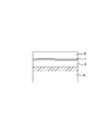
そして、本発明の不通電蒸着方法の実施例は、図1に図示する如く、基材Aと下塗り層2と錫薄膜1とハードコート層3とから構成されるものである。
An embodiment of the non-conductive vapor deposition method of the present invention comprises a substrate A, an
そして、基材Aは金属、樹脂、ガラス等でありモバイル製品のケースや、耐摩耗性が求められるボタン等への加飾や、基板、各種フィルム等であり、本発明の不通電蒸着方法を実施できるものなら構わないものである。 And the base material A is a metal, resin, glass etc., and is a decoration of a mobile product case, a button etc. where abrasion resistance is required, a substrate, various films, etc. Anything that can be implemented is acceptable.
そして、下塗り層2を形成する工程は後述する錫薄膜1を形成するため下塗りであり、基材Aの表面にUV硬化性樹脂又は1液アクリルシリコン樹脂を吹き付け塗装又はデッピンク塗装又はスピンコート又はインモールド転写又は熱転写等で1〜50ミクロンの厚さの下塗り層2を形成するものである。
The step of forming the
次に、錫薄膜1を形成する工程は、前記下塗り層2を形成する工程で形成した下塗り層2の上面に前述の錫薄膜1を形成する工程を実施するものである。
Next, the step of forming the tin thin film 1 is a step of forming the above-described tin thin film 1 on the upper surface of the
次いで、ハードコート層3を形成する工程では、前記錫薄膜1の上面に1液アクリルシリコン樹脂又は2液アクリルシリコン樹脂又は1液アクリルウレタン樹脂又は2液アクリルウレタン樹脂又は2液塩ビ系樹脂又はUV硬化性樹脂で膜厚が1〜50ミクロンのハードコート層3を形成するものであり、ハードコート層3は耐摩耗性や耐候性、信頼性に優れているものが良好で、薄膜の錫薄膜1を保護するものである。
Next, in the step of forming the
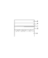
更に、本発明の不通電蒸着方法の次実施例は、図2に図示する如く、中塗り層4を錫薄膜1とハードコート層3との間に形成するもので、つまり、基材Aと下塗り層2と錫薄膜1と中塗り層4とハードコート層3とから構成されるものである。
Further, in the next embodiment of the non-conductive vapor deposition method of the present invention, as shown in FIG. 2, an intermediate coating layer 4 is formed between the tin thin film 1 and the
更には、中塗り層4を形成する工程では、錫薄膜1は膜厚は500オームストロング以下と非常に薄い膜であり、錫薄膜1をハードコート層3と共に保護するためものであり、中塗り層4は錫薄膜1の上面に1液アクリルシリコン樹脂又は2液アクリルシリコン樹脂又は1液アクリルウレタン樹脂又は2液アクリルウレタン樹脂又は2液塩ビ系樹脂又はUV硬化性樹脂で膜厚が1〜50ミクロンに形成するものである。
Further, in the step of forming the intermediate coating layer 4, the tin thin film 1 is a very thin film having a thickness of 500 ohms or less, and is intended to protect the tin thin film 1 together with the
そして、中塗り層4を形成する工程で形成した中塗り層4の上面にハードコート層3を形成する工程を実施してハードコート層3を形成するものである。
And the process of forming the hard-
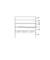
更に、本発明の不通電蒸着方法の他の実施例は、図3に図示する如く、次実施例に加えて、加飾部5と上塗り層6とを中塗り層4とハードコート層3との間に形成するもので、つまり、基材Aと下塗り層2と錫薄膜1と中塗り層4と加飾部5と上塗り層6とハードコート層3とから構成されるものである。
Furthermore, as shown in FIG. 3, another embodiment of the non-conductive vapor deposition method of the present invention includes a decorative portion 5 and a top coat layer 6, an intermediate coat layer 4, a
次いで、加飾部5を形成する工程は前記中塗り層4を形成する工程で形成させた中塗り層4の上面にレザーマーキング又は印刷又はホットスタンプで加飾部5を形成するもので、レザーマーキングの場合はレザーを照射することで中塗り層4及び錫薄膜1を刻設するもので、印刷又はホットスタンプの場合は中塗り層4の上面に加飾するものである。 Subsequently, the process of forming the decoration part 5 forms the decoration part 5 by the leather marking or printing or a hot stamp on the upper surface of the intermediate coating layer 4 formed at the process of forming the said intermediate coating layer 4, In the case of marking, the intermediate coating layer 4 and the tin thin film 1 are engraved by irradiating leather, and in the case of printing or hot stamping, the upper surface of the intermediate coating layer 4 is decorated.
更には、上塗り層6を形成する工程は、前記加飾部5の上面に1液アクリルシリコン樹脂又は2液アクリルシリコン樹脂又は1液アクリルウレタン樹脂又は2液アクリルウレタン樹脂又は2液塩ビ系樹脂又はUV硬化性樹脂で膜厚が1〜50ミクロンの上塗り層6を形成するものである。 Furthermore, the step of forming the overcoat layer 6 includes the step of forming a one-part acrylic silicon resin, a two-part acrylic silicon resin, a one-part acrylic urethane resin, a two-part acrylic urethane resin, or a two-part vinyl chloride resin on the upper surface of the decorative portion 5. The overcoat layer 6 having a film thickness of 1 to 50 microns is formed of a UV curable resin.
次に、前述と同様に、上塗り層6の上面にハードコート層3を形成する工程を実施してハードコート層3を形成するものである。
Next, the
本発明の不通電蒸着方法は、99.99%以上の純度の錫を用いて、膜厚が500オングストロング以下の錫薄膜をフィラメント式真空蒸着法又はエレクトリックビーム式又はイオンプレーティング装置又はスパッタリング装置により形成することによって、錫薄膜が不通電と成るもので、基材の表面の加飾のみならず、今後、あらゆる分野での用途が検討されるものである。 The non-conductive vapor deposition method of the present invention uses a tin film having a thickness of 500 angstroms or less using tin having a purity of 99.99% or more, a filament type vacuum deposition method, an electric beam type, an ion plating device, or a sputtering device. As a result, the tin thin film becomes non-energized, and not only decorating the surface of the base material but also its use in various fields will be studied in the future.
A 基材
1 錫薄膜
2 下塗り層
3 ハードコート層
4 中塗り層
5 加飾部
6 上塗り層
A base material 1 tin
Claims (4)
A process of forming an undercoat layer of 1 to 50 microns of UV curable resin or one-part acrylic silicon resin by spray coating, dipper coating, spin coating, in-mold transfer, thermal transfer, or the like on the surface of a substrate such as metal, resin, glass, etc. And a thickness of 500 angstroms as measured by an electron force microscope using a filament-type vacuum deposition method, an electric beam method, an ion plating device or a sputtering device using tin having a purity of 99.99% or more on the upper surface of the undercoat layer. A step of forming a strong tin film or less, a one-part acrylic silicon resin, a two-part acrylic silicon resin, a one-part acrylic urethane resin, a two-part acrylic urethane resin, a two-part vinyl chloride resin, or a UV curable resin on the upper surface of the tin thin film A step of forming an intermediate coating layer of 1 to 50 microns with a resin, and a top surface of the intermediate coating layer; -A step of forming a decorative part by marking, printing or hot stamping, and a one-part acrylic silicon resin, two-part acrylic silicon resin, one-part acrylic urethane resin, two-part acrylic urethane resin or two-part vinyl chloride on the upper surface of the decorative part Forming an overcoat layer of 1 to 50 microns with a base resin or a UV curable resin, and a one-part acrylic silicon resin, a two-part acrylic silicon resin, a one-part acrylic urethane resin, or a two-part acrylic urethane resin on the top surface of the overcoat layer Or a step of forming a hard coat layer of 1 to 50 microns with a two-part vinyl chloride resin or a UV curable resin, wherein the tin thin film is non-conductive.
Priority Applications (1)
| Application Number | Priority Date | Filing Date | Title |
|---|---|---|---|
| JP2004117998A JP2005298917A (en) | 2004-04-13 | 2004-04-13 | Non-conductive deposition method |
Applications Claiming Priority (1)
| Application Number | Priority Date | Filing Date | Title |
|---|---|---|---|
| JP2004117998A JP2005298917A (en) | 2004-04-13 | 2004-04-13 | Non-conductive deposition method |
Publications (1)
| Publication Number | Publication Date |
|---|---|
| JP2005298917A true JP2005298917A (en) | 2005-10-27 |
Family
ID=35330827
Family Applications (1)
| Application Number | Title | Priority Date | Filing Date |
|---|---|---|---|
| JP2004117998A Pending JP2005298917A (en) | 2004-04-13 | 2004-04-13 | Non-conductive deposition method |
Country Status (1)
| Country | Link |
|---|---|
| JP (1) | JP2005298917A (en) |
Cited By (2)
| Publication number | Priority date | Publication date | Assignee | Title |
|---|---|---|---|---|
| JP2007268323A (en) * | 2006-03-30 | 2007-10-18 | Fukuda Corporation:Kk | Method for decorating magnesium alloy molded products |
| JP2011189322A (en) * | 2010-03-16 | 2011-09-29 | Fukuda Corporation:Kk | Decorating method |
-
2004
- 2004-04-13 JP JP2004117998A patent/JP2005298917A/en active Pending
Cited By (2)
| Publication number | Priority date | Publication date | Assignee | Title |
|---|---|---|---|---|
| JP2007268323A (en) * | 2006-03-30 | 2007-10-18 | Fukuda Corporation:Kk | Method for decorating magnesium alloy molded products |
| JP2011189322A (en) * | 2010-03-16 | 2011-09-29 | Fukuda Corporation:Kk | Decorating method |
Similar Documents
| Publication | Publication Date | Title |
|---|---|---|
| KR0180910B1 (en) | Transparent plane heater and its manufacturing method | |
| US8367434B2 (en) | Method for fabricating a nanostructured substrate for OLED and method for fabricating an OLED | |
| CA2054931A1 (en) | Fluorocarbon-based polymer lamination coating film and method of manufacturing the same | |
| KR940013627A (en) | Manufacturing method of brightly colored high gloss plastic products | |
| TW201119866A (en) | Transparent conductive film, method for production thereof and touch panel therewith | |
| CN105723817A (en) | Flexible printed circuit board and method for manufacturing same | |
| TW201522694A (en) | Flexible compound, its method and application | |
| CN101522469A (en) | A method of depositing an abrasion-resistant layer onto an electroluminescent plastic window | |
| US20160234930A1 (en) | Stretchable transparent electrode and method of fabricating same | |
| JP2015525146A (en) | PVD coating embedded in lacquer coating | |
| TWI298354B (en) | Method for producing smooth indium-tin-oxide layers on substrates and a substrate coating of indium-tin-oxide | |
| EP1342509A3 (en) | Process for forming multi-layered coatings and multi-layered coating | |
| JP6489016B2 (en) | Electronic device and manufacturing method thereof | |
| JP2005298917A (en) | Non-conductive deposition method | |
| JPH0888077A (en) | Transparent sheet heater and manufacturing method thereof | |
| KR102189938B1 (en) | Stretchable electrode, method of fabricating the same and flexible electronic device having the same | |
| JP5562283B2 (en) | Transparent conductive material comprising transparent conductive film mainly composed of graphene and method for producing the same | |
| TW202029832A (en) | Heater and article with heater | |
| JP3325361B2 (en) | Transparent planar heater and method of manufacturing the same | |
| US20060255492A1 (en) | In-mold decoration process | |
| WO2009017376A2 (en) | Process for manufacturing multi-layered thin film by dry vacuum vapor deposition | |
| JP2006001160A (en) | How to decorate molded products of different materials | |
| US20050168141A1 (en) | Method for producing an electronic component and a display | |
| JPH06338381A (en) | Transparent sheet-like heater and manufacture thereof | |
| JP4848758B2 (en) | Non-contact IC tag with insulating metal layer |
Legal Events
| Date | Code | Title | Description |
|---|---|---|---|
| A621 | Written request for application examination |
Free format text: JAPANESE INTERMEDIATE CODE: A621 Effective date: 20070510 |
|
| A072 | Dismissal of procedure |
Effective date: 20070925 Free format text: JAPANESE INTERMEDIATE CODE: A072 |