JP2005298875A - Ferritic film, supporting body using the same, electronic circuit board, and semi-conductor integrated wafer - Google Patents
Ferritic film, supporting body using the same, electronic circuit board, and semi-conductor integrated wafer Download PDFInfo
- Publication number
- JP2005298875A JP2005298875A JP2004114371A JP2004114371A JP2005298875A JP 2005298875 A JP2005298875 A JP 2005298875A JP 2004114371 A JP2004114371 A JP 2004114371A JP 2004114371 A JP2004114371 A JP 2004114371A JP 2005298875 A JP2005298875 A JP 2005298875A
- Authority
- JP
- Japan
- Prior art keywords
- ferrite film
- film
- coating layer
- insulating
- ferrite
- Prior art date
- Legal status (The legal status is an assumption and is not a legal conclusion. Google has not performed a legal analysis and makes no representation as to the accuracy of the status listed.)
- Pending
Links
Images
Landscapes
- Other Surface Treatments For Metallic Materials (AREA)
- Thin Magnetic Films (AREA)
- Non-Metallic Protective Coatings For Printed Circuits (AREA)
- Shielding Devices Or Components To Electric Or Magnetic Fields (AREA)
- Waveguides (AREA)
Abstract
Description
本発明は、フェライト膜に関し、特に、インダクタンス素子、インピーダンス素子、磁気ヘッド、マイクロ波素子、磁歪素子、及び高周波領域において不要電磁波の干渉によって生じる電磁障害を抑制するために用いられる電磁干渉抑制体などの高周波磁気デバイスに特に利用価値の高いスピネル型フェライト膜に関する。 The present invention relates to a ferrite film, and in particular, an inductance element, an impedance element, a magnetic head, a microwave element, a magnetostrictive element, and an electromagnetic interference suppressor used for suppressing electromagnetic interference caused by interference of unnecessary electromagnetic waves in a high frequency region. The present invention relates to a spinel type ferrite film that is particularly useful for high frequency magnetic devices.
フェライトメッキとは、固体表面にフェライト膜を形成することをいう(例えば、特許文献1参照)。詳述すると、フェライトメッキは、次のプロセスで行われる。固体表面に、金属イオンとして少なくとも第1鉄イオンを含む水溶液を接触させる。次に、固体表面にFe2+またはこれと他の水酸化金属イオンを吸着せる。続いて、吸着したFe2+を酸化させることによりFe3+を得る。これが水溶液中の水酸化金属イオンとの間でフェライト結晶化反応を起こし、これによって固体表面にフェライト膜を形成する。 Ferrite plating refers to forming a ferrite film on a solid surface (see, for example, Patent Document 1). More specifically, ferrite plating is performed by the following process. An aqueous solution containing at least ferrous ions as metal ions is brought into contact with the solid surface. Next, Fe 2+ or this and other metal hydroxide ions are adsorbed on the solid surface. Subsequently, Fe 3+ is obtained by oxidizing the adsorbed Fe 2+ . This causes a ferrite crystallization reaction with metal hydroxide ions in the aqueous solution, thereby forming a ferrite film on the solid surface.
従来、この技術を基にフェライト膜の均質化、反応速度の向上を図ったもの(例えば、特許文献2参照)、固体表面に界面活性を付与して種々の固体にフェライト膜を形成しようとするもの(例えば、特許文献3参照)、フェライト膜の形成速度の向上に関するもの(例えば、特許文献4、特許文献5、及び特許文献6参照)が知られている。
Conventionally, a ferrite film is homogenized based on this technique and the reaction rate is improved (see, for example, Patent Document 2). An attempt is made to form a ferrite film on various solids by imparting surface activity to the solid surface. There are known ones (for example, see Patent Document 3) and those related to improvement in the formation rate of a ferrite film (for example, see Patent Document 4,
フェライトメッキは、膜を形成しようとする固体が前述した水溶液に対して耐性があれば何でも良い。更に、水溶液を介した反応であるために、温度が比較的低温(常温〜水溶液の沸点以下)でスピネル型フェライト膜を形成できるという特徴がある。そのため、他のフェライト膜作成技術に比べて、固体の限定範囲が小さい。 The ferrite plating may be anything as long as the solid to form a film is resistant to the aqueous solution described above. Furthermore, since the reaction is via an aqueous solution, the spinel ferrite film can be formed at a relatively low temperature (from room temperature to the boiling point of the aqueous solution). Therefore, the limited range of solids is small compared to other ferrite film creation techniques.
しかしながら、インダクタンス素子、インピーダンス素子、磁気ヘッド、マイクロ波素子、磁歪素子、及び高周波領域における電磁干渉抑制体等への応用という観点からみると、従来のフェライト膜は絶縁性が不十分である。その結果、各種電子部品等への応用、あるいは適用等に関して製品の信頼性の面で課題がある。 However, from the viewpoint of application to inductance elements, impedance elements, magnetic heads, microwave elements, magnetostrictive elements, electromagnetic interference suppressors in the high frequency region, etc., conventional ferrite films have insufficient insulation. As a result, there is a problem in terms of product reliability with respect to application to various electronic components or the like.
そこで本発明の目的は、フェライトメッキ法によって形成されるフェライト膜において、係る従来の欠点を解消し、極めて信頼性に優れるフェライト膜およびそれを用いた電磁雑音抑制機能付き支持体、電子配線基板、及び半導体集積ウェハを提供することにある。 Therefore, the object of the present invention is to eliminate the conventional drawbacks in the ferrite film formed by the ferrite plating method, and to provide a highly reliable ferrite film, a support with an electromagnetic noise suppression function using the same, an electronic wiring board, And providing a semiconductor integrated wafer.
本発明者等は、種々検討の結果、フェライト膜の片面または両面を絶縁性の材料でコーティングすることによって、その絶縁性を向上することが出来ることを見出した。 As a result of various studies, the present inventors have found that the insulating properties can be improved by coating one or both surfaces of the ferrite film with an insulating material.
また、本発明者等は、上記フェライト膜を支持体上、電子配線基板上または半導体集積ウェハの少なくとも一方の面に上記コーティング層を介して直接成膜することによって電磁雑音抑制体を実現できることを見出した。 In addition, the present inventors can realize an electromagnetic noise suppressor by directly forming the ferrite film on a support, on an electronic wiring substrate, or on at least one surface of a semiconductor integrated wafer via the coating layer. I found it.
本発明によれば、フェライト膜の片面または両面を絶縁性の材料でコーティングすることによって、その絶縁性を向上させ、電子機器等で使用する場合に不可欠である信頼性を向上することが出来る。また、上記フェライト膜を支持体、電子配線基板上または半導体集積ウェハの少なくとも一面に上記絶縁コーティング層を介して直接成膜することによって、電磁雑音抑制体を実現できる。 According to the present invention, by coating one surface or both surfaces of a ferrite film with an insulating material, the insulating property can be improved, and the reliability that is indispensable when used in an electronic device or the like can be improved. In addition, an electromagnetic noise suppressing body can be realized by directly forming the ferrite film on the support, the electronic wiring substrate or at least one surface of the semiconductor integrated wafer via the insulating coating layer.
以下、本発明の実施の形態について、図面を参照して詳細に説明する。 Hereinafter, embodiments of the present invention will be described in detail with reference to the drawings.
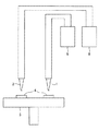
図1に、本発明によるフェライト膜を形成するフェライト膜形成装置を示す。図示のフェライト膜形成装置は、回転台3と、この回転台3上に設定される2つの基体(支持体)4とを有する。この基体4はフェライト膜を形成するためのものである。 FIG. 1 shows a ferrite film forming apparatus for forming a ferrite film according to the present invention. The illustrated ferrite film forming apparatus includes a turntable 3 and two base bodies (supports) 4 set on the turntable 3. This substrate 4 is for forming a ferrite film.
図示のフェライト膜形成装置は、さらに、メッキに必要な液を貯蔵するための第1及び第2のタンク5および6を備える。この第1及び第2のタンク5および6に貯蔵された溶液は、それぞれ、第1及び第2のノズル1および2を介して基体4、4に供給される。その際、例えば、第1のノズル1を介して基体4に溶液が供給された後、供給された溶液が回転台3の回転による遠心力で除去され、第2のノズル2を介して基体4に溶液が供給された後、供給された溶液が回転台3の回転による遠心力で除去されることを繰り返す。
The illustrated ferrite film forming apparatus further includes first and
本実施の形態では、反応液及び酸化液を基体4から除去する際、遠心力を用いているが、重力によって反応液、酸化液に付与される流動性によって反応液及び酸化液を除去しても構わない。 In the present embodiment, centrifugal force is used when removing the reaction solution and the oxidizing solution from the substrate 4, but the reaction solution and the oxidizing solution are removed by the fluidity imparted to the reaction solution and the oxidizing solution by gravity. It doesn't matter.
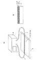
図2を参照して、本発明により得られたフェライト膜の電磁雑音抑制効果について説明する。図2において、(a)はフェライト膜の電磁雑音抑制効果の評価系の全体図を示し、(b)はフェライト膜部分の断面図を示す。 With reference to FIG. 2, the electromagnetic noise suppression effect of the ferrite film obtained by the present invention will be described. 2A is an overall view of the evaluation system for the electromagnetic noise suppression effect of the ferrite film, and FIG. 2B is a cross-sectional view of the ferrite film portion.
図2(a)において、評価系は、マイクロストリップライン(MSL)8を有する。マイクロストリップライン8は、フェライト膜形成時の基体および伝送路として用いられる。図示のマイクロストリップライン8は、厚さ1.6mm、80mm角のガラスエポキシ基板と、そのガラスエポキシ基板の表面中央部に形成された中心導体と、ガラスエポキシ基板の裏面に形成されたグランド導体とから構成されている。中心導体は、幅が約3mmで、ガラスエポキシ基板の全幅80mmに渡って形成されている。マイクロストリップライン8の特性インピーダンスは50Ωである。
In FIG. 2A, the evaluation system has a microstrip line (MSL) 8. The
図2(a)に加えて図2(b)をも参照して、マイクロストリップライン8の表面には、略全面に渡り25μmの厚さの第1のポリイミド膜11−1が直接形成してある。その第1のポリイミド膜11−1の上に、本発明により得られたフェライト膜10が略全面に渡り形成してある。さらに、そのフェライト膜10の上に、略全面に渡り、25μmの厚さの第2のポリイミド膜11−2が直接形成してある。
Referring to FIG. 2B in addition to FIG. 2A, the first polyimide film 11-1 having a thickness of 25 μm is directly formed on the surface of the
また、比較材として、ポリイミド膜を介さずにマイクロストリップライン8上に直接、フェライト膜を成膜した試料も作製した。
As a comparative material, a sample in which a ferrite film was formed directly on the
フェライト膜10の成膜(形成)は以下の条件で行った。図1に示す様なフェライト膜形成装置の回転台3の上に基体4として上記マイクロストリップライン8を置き、回転台3を150rpmの回転数で回転させながら、脱酸素イオン交換水を供給しながら、マイクロストリップライン8を90℃まで加熱した。ついで、フェライト膜形成装置内にN2ガスを導入し脱酸素雰囲気を形成した。
The
反応液として、脱酸素イオン交換水中に、FeCl2・4H2O、NiCl2・6H2O、ZnCl2をそれぞれ3.3g/リットル、1.3g/リットル、0.03g/リットル溶かしたものを準備した。この反応液は第1のタンク5に貯蔵されている。一方、脱酸素イオン交換水中にNaNO2とCH3COONH4をそれぞれ0.3g/リットル、5.0g/リットル溶かした酸化液を第2のタンク6に貯蔵した。この酸化液と上記反応液とを第2及び第1のノズル2、1によりそれぞれ30ミリリットル/分の流量で約180分供給した。
A reaction solution prepared by dissolving 3.3 g / liter, 1.3 g / liter, and 0.03 g / liter of FeCl 2 .4H 2 O, NiCl 2 .6H 2 O, and ZnCl 2 in deoxygenated ion-exchanged water, respectively. Got ready. This reaction solution is stored in the
その後、取り出した各基体4の板上には黒色膜が形成されており、この黒色膜がNi、Zn、Fe、Oからなるフェライトであることを確認した。走査形顕微鏡(SEM)を用いた組織観察の結果、その黒色膜の膜厚が均一である組織が形成されていた。黒色膜の比抵抗は700Ωcmであった。 Thereafter, a black film was formed on the plate of each substrate 4 taken out, and it was confirmed that this black film was a ferrite composed of Ni, Zn, Fe, and O. As a result of the structure observation using a scanning microscope (SEM), a structure in which the film thickness of the black film was uniform was formed. The specific resistance of the black film was 700 Ωcm.
図2(a)において、評価系はネットワークアナライザ9を備えている。電磁雑音抑制効果の測定は、マイクロストリップライン8の両端を、同軸ケーブル7を介してネットワークアナライザ9に接続し、マイクロストリップライン8単体での伝送特性を基準に、マイクロストリップライン8上に試料を配置した場合の伝送特性を求めたものである。
In FIG. 2A, the evaluation system includes a network analyzer 9. In measuring the electromagnetic noise suppression effect, both ends of the
この技術分野において周知のように、伝送特性としてはSパラメータが用いられる。SパラメータのS11は反射係数を示し、S21は透過係数を示す。 As is well known in this technical field, S parameters are used as transmission characteristics. S11 of the S parameter indicates a reflection coefficient, and S21 indicates a transmission coefficient.
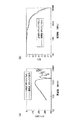
図3は、得られた伝送特性を示した図である。図3において、(a)は反射特性を示し、(b)は透過特性を示す。図3(a)において、横軸は周波数(MHz)を示し、縦軸は反射係数S11(dB)を示す。図3(b)において、横軸は周波数(MHz)を示し、縦軸は透過係数S21を示す。図3(a)及び(b)には、発明品(太い実線で示す)の他に、ポリイミドによる被覆を行わない試料についても比較材(細い実線で示す)として示してある。 FIG. 3 is a diagram illustrating the obtained transmission characteristics. In FIG. 3, (a) shows reflection characteristics, and (b) shows transmission characteristics. In FIG. 3A, the horizontal axis indicates the frequency (MHz), and the vertical axis indicates the reflection coefficient S11 (dB). In FIG. 3B, the horizontal axis indicates the frequency (MHz), and the vertical axis indicates the transmission coefficient S21. In FIGS. 3A and 3B, in addition to the inventive product (indicated by a thick solid line), a sample not coated with polyimide is also shown as a comparative material (indicated by a thin solid line).
図3(a)から、比較材と比較して、発明品はフェライト膜試料を大面積に形成したにも拘わらず、十分に低い値の反射係数S11を持つことが分かる。発明品のこの反射係数S11の値は、例えば、実際の電子回路に用いても伝送信号に悪影響を及ぼすことは無いレベルだと考えられる。 From FIG. 3A, it can be seen that the invention product has a sufficiently low value of the reflection coefficient S11 even though the ferrite film sample is formed in a large area as compared with the comparative material. The value of the reflection coefficient S11 of the invention is considered to be a level that does not adversely affect the transmission signal even when used in an actual electronic circuit, for example.
図3(b)から、比較材と比較して、発明品は高周波側で透過係数S21が大きく減衰していることが確認できる。 From FIG. 3B, it can be confirmed that the transmission coefficient S21 of the inventive product is greatly attenuated on the high frequency side as compared with the comparative material.
これらの結果より、本発明によるフェライト膜を伝送線路に形成することで、そのフェライト膜は、電子機器内で生じる高周波のノイズを減衰させる電磁雑音抑制体として有効であることが分かる。さらに、この発明品の伝送特性はフェライト膜の面積、膜厚やその組成を変えることで、所望の特性に調整することが可能である。 From these results, it can be seen that by forming the ferrite film according to the present invention on the transmission line, the ferrite film is effective as an electromagnetic noise suppressing body that attenuates high-frequency noise generated in the electronic device. Furthermore, the transmission characteristics of the product of the present invention can be adjusted to desired characteristics by changing the area, film thickness and composition of the ferrite film.
また、図3(a)および図3(b)から分かるとおり、フェライト膜10とマイクロストリップライン8との間にポリイミド膜11−1を形成することによる特性の変化は非常に小さい。すなわち、ポリイミド膜11−1,11−2である絶縁膜により信頼性は高まり、かつ特性劣化はほとんどない。
Further, as can be seen from FIGS. 3A and 3B, the change in characteristics due to the formation of the polyimide film 11-1 between the
本発明による絶縁性フェライト膜は、優れた絶縁性と高周波帯域における優れた磁気損失特性により、電磁雑音抑制体として使用できる。更にフェライト膜を電子配線基板上または半導体集積ウェハの少なくとも一方の面に絶縁層を介して直接成膜することにより、電磁雑音抑制機能を兼ね備えた電子配線基板または半導体集積ウェハを実現することができる。 The insulating ferrite film according to the present invention can be used as an electromagnetic noise suppressor due to excellent insulating properties and excellent magnetic loss characteristics in a high frequency band. Further, by directly forming a ferrite film on the electronic wiring board or on at least one surface of the semiconductor integrated wafer via an insulating layer, an electronic wiring board or a semiconductor integrated wafer having an electromagnetic noise suppressing function can be realized. .
以上で説明した実施の形態においては、上記絶縁層(絶縁コーティング層)の材料としてポリイミドを用いているが、絶縁性を有するものであればその材料は何でもよい。また、以上で説明した実施の形態においては、上記絶縁層にコーティングされたフェライト膜が1層の場合についてのみ示したが、上記絶縁層を介して複層化したフェライト膜であっても同様の効果が得られる。 In the embodiment described above, polyimide is used as the material of the insulating layer (insulating coating layer), but any material may be used as long as it has insulating properties. Further, in the embodiment described above, only the case where the ferrite film coated on the insulating layer is a single layer is shown, but the same applies to a ferrite film that is multi-layered via the insulating layer. An effect is obtained.
1,2 ノズル
3 回転台
4 基体(支持体)
5,6 タンク
7 同軸ケーブル
8 マイクロストリップライン(MSL)
9 ネットワークアナライザ
10 フェライト膜
11−1,11−2 ポリイミド膜
1, 2 Nozzle 3 Turntable 4 Substrate (support)
5, 6
9
Claims (8)
該フェライト膜の片面または両面を絶縁性の材料でコーティングする工程と
を含む絶縁性フェライト膜の製造方法。 A step of preparing a ferrite film;
A method of manufacturing an insulating ferrite film, comprising: coating one or both surfaces of the ferrite film with an insulating material.
該支持体上に絶縁性材料をコーティングして、絶縁コーティング層を形成する工程と、
前記絶縁コーティング層上にフェライト膜を成膜する工程と
を含む電磁雑音抑制機能付支持体の製造方法。 Preparing a support;
Coating an insulating material on the support to form an insulating coating layer;
And a step of forming a ferrite film on the insulating coating layer.
該電子配線基板上に絶縁性材料をコーティングして、絶縁コーティング層を形成する工程と、
該絶縁コーティング層上にフェライト膜を成膜する工程と
を含む電磁雑音抑制機能付電子配線基板の製造方法。 Preparing an electronic wiring board;
Coating an insulating material on the electronic wiring board to form an insulating coating layer;
A method of manufacturing an electronic wiring board with an electromagnetic noise suppression function, comprising a step of forming a ferrite film on the insulating coating layer.
該半導体集積ウェハの少なくとも一方の面に絶縁性材料をコーティングして、絶縁コーティング層を形成する工程と、
該絶縁コーティング層上にフェライト膜を成膜する工程と
を含む電磁雑音抑制機能付半導体集積ウェハの製造方法。
A step of preparing a semiconductor integrated wafer;
Coating an insulating material on at least one surface of the semiconductor integrated wafer to form an insulating coating layer;
A method of manufacturing a semiconductor integrated wafer with an electromagnetic noise suppression function, comprising: forming a ferrite film on the insulating coating layer.
Priority Applications (1)
| Application Number | Priority Date | Filing Date | Title |
|---|---|---|---|
| JP2004114371A JP2005298875A (en) | 2004-04-08 | 2004-04-08 | Ferritic film, supporting body using the same, electronic circuit board, and semi-conductor integrated wafer |
Applications Claiming Priority (1)
| Application Number | Priority Date | Filing Date | Title |
|---|---|---|---|
| JP2004114371A JP2005298875A (en) | 2004-04-08 | 2004-04-08 | Ferritic film, supporting body using the same, electronic circuit board, and semi-conductor integrated wafer |
Publications (1)
| Publication Number | Publication Date |
|---|---|
| JP2005298875A true JP2005298875A (en) | 2005-10-27 |
Family
ID=35330787
Family Applications (1)
| Application Number | Title | Priority Date | Filing Date |
|---|---|---|---|
| JP2004114371A Pending JP2005298875A (en) | 2004-04-08 | 2004-04-08 | Ferritic film, supporting body using the same, electronic circuit board, and semi-conductor integrated wafer |
Country Status (1)
| Country | Link |
|---|---|
| JP (1) | JP2005298875A (en) |
Cited By (2)
| Publication number | Priority date | Publication date | Assignee | Title |
|---|---|---|---|---|
| JP2013004947A (en) * | 2011-06-22 | 2013-01-07 | Nec Tokin Corp | Interposer |
| US9991051B2 (en) | 2008-11-12 | 2018-06-05 | Tokin Corporation | Body with magnetic film attached and manufacturing method thereof |
-
2004
- 2004-04-08 JP JP2004114371A patent/JP2005298875A/en active Pending
Cited By (2)
| Publication number | Priority date | Publication date | Assignee | Title |
|---|---|---|---|---|
| US9991051B2 (en) | 2008-11-12 | 2018-06-05 | Tokin Corporation | Body with magnetic film attached and manufacturing method thereof |
| JP2013004947A (en) * | 2011-06-22 | 2013-01-07 | Nec Tokin Corp | Interposer |
Similar Documents
| Publication | Publication Date | Title |
|---|---|---|
| CN110603908A (en) | Electronic component having electromagnetic shield and method for manufacturing the same | |
| US20060038630A1 (en) | Electromagnetic noise suppressor, structure with electromagnetic noise suppressing function, and method of manufacturing the same | |
| US20090061256A1 (en) | Ferrite thin film, method of manufacturing the same and electromagnetic noise suppressor using the same | |
| JP6585032B2 (en) | Printed wiring board substrate, printed wiring board, and printed wiring board manufacturing method | |
| JP2001223493A (en) | Radio wave absorber | |
| CN101480112B (en) | Noise suppression wiring components and printed circuit boards | |
| EP1143774B1 (en) | Wiring board comprising granular magnetic film | |
| JP2005298875A (en) | Ferritic film, supporting body using the same, electronic circuit board, and semi-conductor integrated wafer | |
| KR20190023680A (en) | Multi-layered ferrite film and manufacturing method thereof | |
| KR20140108113A (en) | Method for forming metal film, conductive ink used in the method, multilayer wiring board, semiconductor substrate, and capacitor cell | |
| CN101909419B (en) | A kind of transmission line electromagnetic noise suppressor and preparation method thereof | |
| JP4997484B2 (en) | Ferrite film, manufacturing method thereof, and electromagnetic noise suppressor using the same | |
| TW561607B (en) | Electromagnetic noise suppressor, semiconductor device using the same, and method of manufacturing said semiconductor device | |
| JP2005129766A (en) | Print circuit board and method for manufacturing the same | |
| JP5591587B2 (en) | Noise suppressing transmission line and sheet-like structure used therefor | |
| CN102159749B (en) | Ferrite-coated body and process for production thereof | |
| KR101381345B1 (en) | Multilayer printed circuit board | |
| JP5128050B2 (en) | Manufacturing method of flexible flat cable | |
| JP2005129764A (en) | Electromagnetic interference suppressor and method for manufacturing the same | |
| JP2004111477A (en) | Ferrite thin film and its manufacturing method, and electromagnetic noise suppressor using same | |
| CN218772519U (en) | PCB surface structure and PCB | |
| JP4110286B2 (en) | Method for evaluating soft magnetic properties of ferrite thin film, method for producing ferrite thin film | |
| JP4697928B2 (en) | Ferrite thin film for electromagnetic interference suppressor | |
| JP4251482B2 (en) | Electromagnetic interference suppressor | |
| TWI419635B (en) | Multilayer printed circuit board |
Legal Events
| Date | Code | Title | Description |
|---|---|---|---|
| A621 | Written request for application examination |
Free format text: JAPANESE INTERMEDIATE CODE: A621 Effective date: 20061016 |
|
| A711 | Notification of change in applicant |
Free format text: JAPANESE INTERMEDIATE CODE: A711 Effective date: 20080226 |
|
| A977 | Report on retrieval |
Free format text: JAPANESE INTERMEDIATE CODE: A971007 Effective date: 20080402 |
|
| A131 | Notification of reasons for refusal |
Free format text: JAPANESE INTERMEDIATE CODE: A131 Effective date: 20090408 |
|
| A02 | Decision of refusal |
Free format text: JAPANESE INTERMEDIATE CODE: A02 Effective date: 20090826 |