JP2005296030A - Magnetic field measuring device - Google Patents
Magnetic field measuring device Download PDFInfo
- Publication number
- JP2005296030A JP2005296030A JP2004111908A JP2004111908A JP2005296030A JP 2005296030 A JP2005296030 A JP 2005296030A JP 2004111908 A JP2004111908 A JP 2004111908A JP 2004111908 A JP2004111908 A JP 2004111908A JP 2005296030 A JP2005296030 A JP 2005296030A
- Authority
- JP
- Japan
- Prior art keywords
- bias
- magnetic field
- bias current
- signal
- squid magnetometers
- Prior art date
- Legal status (The legal status is an assumption and is not a legal conclusion. Google has not performed a legal analysis and makes no representation as to the accuracy of the status listed.)
- Granted
Links
Images
Landscapes
- Geophysics And Detection Of Objects (AREA)
- Measurement And Recording Of Electrical Phenomena And Electrical Characteristics Of The Living Body (AREA)
- Measuring Magnetic Variables (AREA)
Abstract
【課題】
複数SQUID磁束計を同時に安定に動作できる磁場計測装置を提供する。
【解決手段】
検出コイルを具備する複数SQUID磁束計12を有する磁場計測装置において、全CHに共通の単一の発振器13によりACバイアスを行う発振周波数を決定する。発振器からの信号を基準としてスイッチSW0、SW1、SW2、SW3、SW4、SW5を切り替え、ACバイアス信号、キャンセル電圧信号、オスセット磁束信号の印加を選択する。プラス側のバイアス電流の時のV−Φ特性とマイナス側の電流バイアスの時のV−Φ特性を用いて相互相関関数を用いる手法、又は、ACバイアスを行なっているV−Φ特性をスペクトル解析する手法に基づいて、ACバイアス信号の自動調整を行なう。
【選択図】 図2
【Task】
Provided is a magnetic field measuring apparatus capable of simultaneously and stably operating a plurality of SQUID magnetometers.
[Solution]
In a magnetic field measurement apparatus having a plurality of SQUID magnetometers 12 having detection coils, an oscillation frequency for performing AC bias is determined by a single oscillator 13 common to all CHs. The switches SW0, SW1, SW2, SW3, SW4, and SW5 are switched based on the signal from the oscillator, and the application of the AC bias signal, the cancel voltage signal, and the male set magnetic flux signal is selected. Spectral analysis of V-Φ characteristics with positive bias current and V-Φ characteristics with negative current bias using cross-correlation function, or V-Φ characteristics with AC bias The AC bias signal is automatically adjusted based on the technique to be performed.
[Selection] Figure 2
Description
本発明は、心臓磁場、脳磁場等の生体磁場計測、地磁気計測、非破壊検査等の微弱磁場計測を行なう超伝導デバイスであるSQUID(Superconducting Quantum Interference Device:超伝導量子干渉素子)磁束計を用いた磁場計測技術に関する。 The present invention uses a SQUID (Superconducting Quantum Interference Device) magnetometer, which is a superconducting device for measuring weak magnetic fields such as biomagnetic field measurements such as cardiac magnetic fields and brain magnetic fields, geomagnetic measurements, and non-destructive inspections. Related to magnetic field measurement technology.
高温超電導SQUIDを用いた磁場計測装置では、高温超電導部材内のトラップ磁束による揺らぎによるノイズ等を低減させるために、通常、電流バイアスをACバイアス電流(バイアス電流をプラス側とマイナス側に交互に変化させる方法)として印加する(例えば、非特許文献1を参照)。この従来方法では、ACバイアス電流を加える発振周波数を上昇させると、高温超電導SQUIDの感度特性が向上することが提案されている。 In a magnetic field measurement device using a high-temperature superconducting SQUID, in order to reduce noise due to fluctuations caused by trapped magnetic flux in the high-temperature superconducting member, the current bias is usually changed to an AC bias current (the bias current is changed alternately between the positive side and the negative side) (See, for example, Non-Patent Document 1). In this conventional method, it is proposed that the sensitivity characteristic of the high-temperature superconducting SQUID is improved when the oscillation frequency to which the AC bias current is applied is increased.
しかし、ACバイアス電流を使用してマルチチャネルに適応した場合の回路構成に関する具体的方法、ACバイアス電流値、オフセット電圧量、キャンセル磁束量を自動で調整する具体的手法については言及がない。 However, there is no mention of a specific method related to a circuit configuration when adapting to multichannel using an AC bias current, and a specific method of automatically adjusting an AC bias current value, an offset voltage amount, and a canceling magnetic flux amount.
ACバイアス電流をSQUID磁束計に印加するために、発振器を各チャネル(以下、CHと略記する)毎に配置すると、それぞれの発振器間に微妙な位相差が生じ、チャープ信号のようなノイズが発生する。チャープ信号は、各CH間で完全にクロストークがない理想的な回路構成であれば生じないが、実際の回路構成では、ACバイアスの発振周波数の信号によるクロストークは無視できない。そのため、安定に複数の高温超電導SQUIDを安定に動作させるACバイアス方式が望まれている。 If an oscillator is arranged for each channel (hereinafter abbreviated as CH) in order to apply an AC bias current to the SQUID magnetometer, a subtle phase difference occurs between the oscillators, and noise such as a chirp signal is generated. To do. A chirp signal does not occur in an ideal circuit configuration in which there is no complete crosstalk between the CHs. However, in an actual circuit configuration, crosstalk due to an AC bias oscillation frequency signal cannot be ignored. Therefore, an AC bias system that stably operates a plurality of high-temperature superconducting SQUIDs is desired.
また、ACバイアス方式では、自動で高温超電導SQUID磁束計の調整を行なうことが困難であるという課題があった。なぜなら、ACバイアス方式を行なう場合、プラスバイアス時とマイナスバイアス時の位相差の磁束量を各CH毎に調整しなければならないためである。また、妨害磁気雑音の多い環境下では、前述の位相差を検出することは困難であるという課題を有していた。 Further, the AC bias method has a problem that it is difficult to automatically adjust the high-temperature superconducting SQUID magnetometer. This is because when performing the AC bias method, the amount of magnetic flux of the phase difference between the plus bias and the minus bias must be adjusted for each CH. In addition, there is a problem that it is difficult to detect the above-described phase difference in an environment with a lot of disturbing magnetic noise.
本発明の目的は、複数SQUID磁束計を同時に安定に動作できる磁場計測技術を提供することにある。 An object of the present invention is to provide a magnetic field measurement technique capable of simultaneously operating a plurality of SQUID magnetometers stably.
上記目的を達成するために、本発明の磁場計測装置は、検査対象から発生する磁場を検出する検出コイルを具備する複数のSQUID磁束計を有し、ACバイアスを行う発振周波数を決定するための発振器を全CH共通に1つだけを有する構成とする。発振器から発生する信号に基づいてスイッチを切り替えるスイッチ切り替え手段を有し、スイッチ切り替え手段によって、ACバイアス信号、キャンセル電圧信号、オフセット磁束信号の印加を選択できる構成とする。この構成により、複数の発振器を使用する必要がないため、雑音となるチャープ信号を生じることはない。 In order to achieve the above object, a magnetic field measurement apparatus of the present invention has a plurality of SQUID magnetometers having detection coils for detecting a magnetic field generated from an inspection object, and determines an oscillation frequency for performing an AC bias. The oscillator is configured to have only one common to all CHs. A switch switching unit that switches a switch based on a signal generated from an oscillator is provided, and an application of an AC bias signal, a cancel voltage signal, and an offset magnetic flux signal can be selected by the switch switching unit. With this configuration, since it is not necessary to use a plurality of oscillators, a chirp signal that becomes noise is not generated.
また、複数のSQUID磁束計に対する、ACバイアス電流値の自動調整方法は、プラス側のバイアス電流の時のV−Φ特性とマイナス側の電流バイアスの時のV−Φ特性を用いて相互相関関数を用いる手法、又は、ACバイアスを行なっているV−Φ特性をスペクトル解析する手法に基づく構成とする。相互相関関数を用いる手法やスペクトル解析する手法を用いることによって、自動で簡易にSQUID磁束計のACバイアス電流動作を実現できる。 Further, the automatic adjustment method of the AC bias current value for a plurality of SQUID magnetometers is based on the cross-correlation function using the V-Φ characteristic when the bias current is positive and the V-Φ characteristic when the current bias is negative. Or a method based on a spectrum analysis of a V-Φ characteristic in which AC bias is performed. The AC bias current operation of the SQUID magnetometer can be realized automatically and simply by using a method using a cross-correlation function or a method of spectrum analysis.
本発明によれば、複数SQUID磁束計を同時に安定に動作できる磁場計測装置を実現できる。 ADVANTAGE OF THE INVENTION According to this invention, the magnetic field measuring apparatus which can operate | move the multiple SQUID magnetometer stably simultaneously simultaneously is realizable.
本発明の磁場計測装置は、検査対象から発生する磁場を検出する検出コイルを具備する複数のSQUID磁束計と、複数のSQUID磁束計にACバイアス電流を印加するための単一の発振器の信号を複数のSQUIDに共通に供給する手段とを有し、この単一の発振器から発生される基準信号に基づいて、ACバイアス信号、キャンセル電圧信号、オフセット磁束信号の印加を選択して制御する手段を有する。 The magnetic field measurement apparatus of the present invention includes a plurality of SQUID magnetometers having a detection coil for detecting a magnetic field generated from an inspection object, and a signal of a single oscillator for applying an AC bias current to the plurality of SQUID magnetometers. Means for commonly supplying a plurality of SQUIDs, and means for selectively controlling the application of an AC bias signal, a cancel voltage signal, and an offset magnetic flux signal based on a reference signal generated from the single oscillator. Have.
検査対象から発生する磁場を検出する検出コイルを具備する複数のSQUID磁束計へのACバイアス電流の印加は、単一の発振器から発生される基準信号に基づいて実行される。この基準信号は複数のSQUIDに対して共通に供給され、複数のSQUID磁束計にACバイアス電流が印加される。プラス側のACバイアス電流の印加時に測定されるV−Φ特性とマイナス側のACバイアス電流の印加時に測定されるV−Φ特性との間の相互相関関数を計算する手段を有し、相互相関関数が最大値を与える時点で印加されている外部磁束を用いて、プラス側のACバイアス電流の印加時とマイナス側のACバイアス電流の印加時の磁束の位相差をキャンセルできる。即ち、相互相関関数が最大値に基づいて、プラス側のACバイアス電流の印加時とマイナス側のACバイアス電流の印加時の磁束の位相差をキャンセルできる。 Application of an AC bias current to a plurality of SQUID magnetometers having a detection coil for detecting a magnetic field generated from a test object is performed based on a reference signal generated from a single oscillator. This reference signal is commonly supplied to a plurality of SQUIDs, and an AC bias current is applied to the plurality of SQUID magnetometers. Means for calculating a cross-correlation function between a V-Φ characteristic measured when a positive AC bias current is applied and a V-Φ characteristic measured when a negative AC bias current is applied, Using the external magnetic flux applied when the function gives the maximum value, the phase difference between the magnetic fluxes when the positive AC bias current is applied and when the negative AC bias current is applied can be canceled. That is, based on the maximum value of the cross-correlation function, the phase difference between the magnetic fluxes when the positive AC bias current is applied and when the negative AC bias current is applied can be canceled.
また、ACバイアス電流の印加時に測定されるV−Φ特性のパワースペクトラムの低周波成分が最大となる位相差を求めることにより、プラス側のACバイアス電流の印加時とマイナス側のACバイアス電流の印加時における磁束の位相差をキャンセルできる。 Further, by obtaining the phase difference that maximizes the low frequency component of the power spectrum of the V-Φ characteristic measured when the AC bias current is applied, the positive side AC bias current and the negative side AC bias current are The phase difference of magnetic flux at the time of application can be canceled.
以下、本発明の実施例について、図面を参照して詳細に説明する。 Hereinafter, embodiments of the present invention will be described in detail with reference to the drawings.
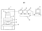
図1は、本発明の実施例になる磁場計測装置の全体構成例を示す図である。 FIG. 1 is a diagram showing an example of the overall configuration of a magnetic field measuring apparatus according to an embodiment of the present invention.
磁気シールドルーム1内にベッド6が配置され、ベッド6の上には被験者5が横たわる。被験者5の上部には、ガントリー4によって保持固定されているクライオスタット3が設置してある。クライオスタット3内部には検出コイルを具備するSQUID磁束計が配置してあり、被験者5の心臓や脳等から発生する微弱な磁場を検出する。SQUIDは、クライオスタット3の上部に設置してあるプリアンプ2を介して、駆動回路7とアンプ・フィルター回路8を通った後、ADコンバーター9に入力されデジタルデータとしてコンピューター11に格納される。また、駆動回路7、アンプ・フィルター回路8、ADコンバーター9はインターフェースボード10を介してコンピューター11によって制御される。デジタルデータとしてコンピューター11に格納された検出された生体磁場データに対して、以下に説明する各種の演算処理が施される。
A
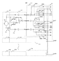
図2は、本発明の実施例の磁場計測装置の回路構成例を示す図である。 FIG. 2 is a diagram illustrating a circuit configuration example of the magnetic field measurement apparatus according to the embodiment of the present invention.
図2に示す磁場計測装置の回路は、1CHからNCH(Nチャネル)から構成されており、インターフェースボード10のみ1枚の構成で全CHを同時にコントロールしている。低温部3−i(i=1、2、〜、N)に配置される高温超電導SQUID12とフィードバックコイルF1は、図1に示したクライオスタット3上部に配置されるプリアンプ部2−i(i=1、2、〜、N)を通して駆動回路部7−i(i=1、2、〜、N)でコントロールされ、磁束計としてSQUID12は動作する。プリアンプ部2−i(i=1、2、〜、N)では、プリアンプ入力の電圧性雑音を低減させるため、プリアンプ(LT1028)を並列に10個接続した構成としている。プリアンプを並列接続したことで、プリアンプの電圧性雑音を0.5nV/√Hzまで低減することが可能となっている。なお、図2において、低温部3−i(i=2、〜、N)の構成は低温部3−1の構成と同じであり、プリアンプ部2−i(i=2、〜、N)の構成はプリアンプ部2−1の構成と同じであり、駆動回路部7−i(i=2、〜、N)の構成は駆動回路部7−1と同じである。簡単のために図2では、検出コイルは省略している。
The circuit of the magnetic field measurement apparatus shown in FIG. 2 is configured from 1CH to NCH (N channel), and only one
次に、図2に示す駆動回路部7−i(i=1、2、〜、N)について説明を行なう。駆動回路部7−i(i=1、2、〜、N)は、図の上段から、電流バイアス部(1段目)、信号検出部(2段目)、フィードバック部(3段目)の3つにより構成されている。以下、電流バイアス部(1段目)、信号検出部(2段目)、フィードバック部(3段目)の構成について、説明する。 Next, the drive circuit unit 7-i (i = 1, 2,..., N) shown in FIG. 2 will be described. The drive circuit unit 7-i (i = 1, 2,..., N) is arranged from the upper stage of the current bias unit (first stage), signal detection unit (second stage), and feedback unit (third stage). It consists of three. Hereinafter, the configuration of the current bias unit (first stage), the signal detection unit (second stage), and the feedback unit (third stage) will be described.
電流バイアス部(1段目)は、DCバイアス部とACバイアス部とをスイッチSW0によって切り替え使用する。DCバイアスモードを選択した場合、スイッチSW0の上段部のスイッチがONになり、スイッチSW0の下段のスイッチがOFFになる。SW0の選択後、DCバイアス電流を加えるための設定電圧値のデジタルデータD0を入力し、DAコンバーターDA0によってアナログ信号に変換される。一方、ACバイアス部に切り替える場合には、SW0の上段部スイッチをOFFにして、下段部スイッチをONにする。この状態で、ACバイアスを行なうプラス側のバイアス電流を加えるための設定電圧値のデジタルデータD1pと、マイナス側のバイアス電流を加えるための設定電圧値のデジタルデータD1mをインターフェースボード10からDAコンバーターDA1に入力されアナログ電圧へと変換される。アナログ変換された電圧をスイッチSW1によって、プラス側の電圧とマイナス側の電圧とを切り替えて矩形波状の電圧を発生させる。
The current bias unit (first stage) switches between the DC bias unit and the AC bias unit using the switch SW0. When the DC bias mode is selected, the upper switch of the switch SW0 is turned on and the lower switch of the switch SW0 is turned off. After the selection of SW0, digital data D0 of a set voltage value for applying a DC bias current is input and converted into an analog signal by the DA converter DA0. On the other hand, when switching to the AC bias unit, the upper switch of SW0 is turned OFF and the lower switch is turned ON. In this state, digital data D1p of a set voltage value for applying a positive bias current for AC bias and digital data D1m of a set voltage value for applying a negative bias current are sent from the
スイッチSW1の切り替えタイミングは、インターフェースボード10内に一つだけ設置してある発振器13によって制御される。この発振器13は、全CHに対する、ACバイアス制御、後述するキャンセル電圧制御、後述するオフセット磁束量制御のための共通の基準信号を発生する。これにより、各CH間のクロストークを避けることが可能となり、複数個配置した発振器によるチャープ信号ノイズの発生を抑止できる。
The switching timing of the switch SW1 is controlled by an oscillator 13 that is installed in the
信号検出部(2段目)では、積分器(スイッチSW5の回路)の前段にキャンセル電圧を入力する。キャンセル電圧はインターフェースボード10から、プラス側のキャンセル電圧(後述の図5に示すVmp)を加えるための設定電圧値のデジタルデータD2pと、マイナス側のキャンセル電圧(後述の図5に示すVmm)を加えるための設定電圧値のデジタルデータD2mを、DAコンバーターDA2に入力し、アナログ電圧に変換し発振器13によって制御されたスイッチSW2によって、キャンセル電圧を加えて積分器の前でのオフセット電圧をキャンセルすることが可能である。
In the signal detection unit (second stage), a cancel voltage is input before the integrator (circuit of the switch SW5). The cancel voltage includes digital data D2p of a set voltage value for applying a plus-side cancel voltage (Vmp shown in FIG. 5 described later) and a minus-side cancel voltage (Vmm shown in FIG. 5 described later) from the
フィードバック部(3段目)では、フィードバック抵抗F2に行く前に、駆動回路部7−i(i=1、2、〜、N)内で、磁束の位相差(後述の図5に示すΦb)を調整するための位相調整用電圧の印加を行なう構成と、SQUIDのV−Φ特性をモニターするための磁束の印加を行なう構成の2種類のスイッチ(SW3とSW4)を有している。磁束の位相差を調整する電圧の印加を行なうため、インターフェースボード10から、プラス側のキャンセル電圧を加えるための設定電圧値のデジタルデータD3をDAコンバーターDA3に入力しアナログ電圧に変換し、発振器13によって制御されたスイッチSW3によってプラス側だけの矩形波を生じさせ、発生した矩形波をフィードバックループ内に入力する。フィードバックループ内に入力された矩形波の電圧によってバイアスのプラス側の時とマイナス側の時の磁束の位相差(Φb)をキャンセルすることが可能となる。
In the feedback unit (third stage), before going to the feedback resistor F2, the phase difference of magnetic flux (Φb shown in FIG. 5 described later) in the drive circuit unit 7-i (i = 1, 2,..., N). There are two types of switches (SW3 and SW4), which are configured to apply a voltage for adjusting the phase for adjusting the voltage and to apply a magnetic flux for monitoring the V-Φ characteristic of the SQUID. In order to apply a voltage for adjusting the phase difference of the magnetic flux, digital data D3 of a set voltage value for applying a positive-side cancel voltage is input from the
また、SQUIDのV−Φ特性をモニターするための磁束の印加は、設定電圧値のデジタルデータD4をDAコンバーターDA4に入力しアナログ電圧に変換し、図3に示すように、デジタルデータD4を順次変化させてV−Φ特性をモニターすることが可能である。V−Φ特性をモニターする場合は、スイッチSW4はONにし、スイッチSW3はOFFにする。反対に、磁束の位相差を調整する電圧の印加を行なう場合は、スイッチSW4はOFFし、スイッチSW3はONにする。 In addition, the magnetic flux for monitoring the SQUID V-Φ characteristic is applied by inputting the digital data D4 of the set voltage value to the DA converter DA4 and converting it into an analog voltage, and sequentially converting the digital data D4 as shown in FIG. It is possible to monitor the V-Φ characteristic by changing. When monitoring the V-Φ characteristic, the switch SW4 is turned on and the switch SW3 is turned off. On the other hand, when applying a voltage for adjusting the phase difference of the magnetic flux, the switch SW4 is turned off and the switch SW3 is turned on.
上記したACバイアス、キャンセル電圧、磁束の位相差の調整が終わると、スイッチSW6をONにした後、スイッチSW5をOFFにすることによって、SQUID12は磁束計として動作が可能となる。磁束計動作後の出力信号Vouti(i=1、2、〜、N)は各CHに生じる。 When the adjustment of the AC bias, the cancel voltage, and the phase difference between the magnetic fluxes is finished, the switch SW6 is turned on and then the switch SW5 is turned off, so that the SQUID 12 can operate as a magnetometer. The output signal Vouti (i = 1, 2,..., N) after the operation of the magnetometer is generated in each CH.
以上の構成のように、本実施例の構成によれば、マルチチャネルの場合、発振器13を一つだけ持たせることによって、各CH間のクロストークをなくし、複数個の発振器を配置した場合に発生するチャープ雑音信号等の発生を避けることが可能である。 As described above, according to the configuration of the present embodiment, in the case of multi-channel, when only one oscillator 13 is provided, crosstalk between each CH is eliminated, and a plurality of oscillators are arranged. It is possible to avoid the generation of a chirp noise signal and the like.
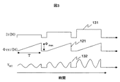
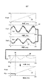
図3は、本発明の実施例の磁場計測装置のV−Φ特性モニター時の制御シーケンスを示す図である。 FIG. 3 is a diagram illustrating a control sequence when monitoring the V-Φ characteristic of the magnetic field measurement apparatus according to the embodiment of the present invention.
図3に示すように、V−Φ特性をモニターする場合、電流バイアスIb(D0)131を段階的に変化させて、各段階の一定の値を有する電流バイアス131の印加時に外部磁束Φext信号(D4)121を三角波(鋸歯状波)の形で入力する。外部磁束Φext信号121は、時間Tの間で0から最大値Φmaxまで直線的に変化する。一定値を有する電流バイアスが印加された状態で外部磁束Φext121が変化すると、出力信号Voutの波形132として正弦波に近い波形が得られる。
As shown in FIG. 3, when the V-Φ characteristic is monitored, the current bias Ib (D0) 131 is changed stepwise, and the external magnetic flux Φext signal (when the
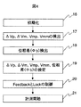
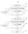
図4は、本発明の実施例の磁場計測装置置のSQUIDの制御手順(ステップ16〜21)を示す図である。
FIG. 4 is a diagram illustrating a SQUID control procedure (
ステップ16:各設定パラメーター(スイッチやデジタルデータ)を初期値に設定する。 Step 16: Set each setting parameter (switch and digital data) to an initial value.
ステップ17:V−Φ特性の変調電圧ΔVpが最大になるプラス方向時のバイアス電流の最適値を求め、その時のキャンセル電圧Vmp(後述の図5を参照)を計算する。同様に、V−Φ特性の変調電圧ΔVmが最大になるマイナス方向時のバイアス電流の最適値を求め、その時のキャンセル電圧Vmm(後述の図5を参照)を計算する(ΔVp、ΔVm、Vmp、Vmmの検出方法については、後述の図6を参照)。 Step 17: An optimum value of the bias current in the plus direction in which the modulation voltage ΔVp of the V-Φ characteristic is maximized is obtained, and a cancel voltage Vmp (see FIG. 5 described later) at that time is calculated. Similarly, the optimum value of the bias current in the negative direction at which the modulation voltage ΔVm of the V-Φ characteristic is maximized is obtained, and the cancel voltage Vmm (see FIG. 5 described later) at that time is calculated (ΔVp, ΔVm, Vmp, For the detection method of Vmm, refer to FIG. 6 described later).
ステップ18:バイアス電流のプラス方向でΔVpが最大になったV−Φ特性と、バイアス電流のマイナス方向でΔVmが最大になったV−Φ特性との位相差(Φb)を検出する(Φbの検出法については、後述の図7と図8を参照)。 Step 18: Detect a phase difference (Φb) between the V-Φ characteristic in which ΔVp is maximum in the positive direction of the bias current and the V-Φ characteristic in which ΔVm is maximum in the negative direction of the bias current (of Φb For the detection method, see FIGS. 7 and 8 described later).
ステップ19:ΔVp、ΔVm、Vmp、Vmm、位相差(Φb)を設定する。 Step 19: ΔVp, ΔVm, Vmp, Vmm, and phase difference (Φb) are set.
ステップ20:FeedbackとLockの制御(スイッチSW6をONにした後、スイッチSW5をOFFにする)を行なう。 Step 20: Feedback and Lock are controlled (switch SW6 is turned on and then switch SW5 is turned off).
ステップ21:計測開始を行なう。 Step 21: Start measurement.
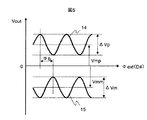
図5は、本発明の実施例の磁場計測装置のV−Φ特性を示す図である。 FIG. 5 is a diagram illustrating the V-Φ characteristics of the magnetic field measurement apparatus according to the embodiment of the present invention.
図6は、本発明の実施例の磁場計測装置の最適なバイアス電流、ΔVp、Vmp、ΔVm、Vmmを求める制御手順を示す図である。 FIG. 6 is a diagram showing a control procedure for obtaining the optimum bias current, ΔVp, Vmp, ΔVm, Vmm of the magnetic field measurement apparatus according to the embodiment of the present invention.
図5、図6を用いて、図4に示すΔVp、ΔVm、Vmp、Vmmの検出方法について説明する。図5は、図3に示す外部磁束Φext(D4)を横軸、図3に示すVoutを縦軸として表示した2次元プロット図である。即ち、図5は、バイアス電流がプラスの状態(Ibp)の時のV−Φ特性14と、バイアス電流がマイナスの状態(Ibm)の時のV−Φ特性15とを示している。図2に示したデジタルデータD2pによって作成されるプラス側のキャンセル電圧は、図5に示すVmpの電圧量と一致させる。同様に、図2に示したデジタルデータD2mによって作成されるマイナス側のキャンセル電圧は、図5に示すVmmの電圧量と一致させる。キャンセル電圧Vmp、Vmmは、バイアス電流がプラスの状態(Ibp)の状態の時のV−Φ特性14から計算する。 A method for detecting ΔVp, ΔVm, Vmp, and Vmm shown in FIG. 4 will be described with reference to FIGS. FIG. 5 is a two-dimensional plot diagram in which the external magnetic flux Φext (D4) shown in FIG. 3 is displayed on the horizontal axis and Vout shown in FIG. 3 is displayed on the vertical axis. That is, FIG. 5 shows the V-Φ characteristic 14 when the bias current is positive (Ibp) and the V-Φ characteristic 15 when the bias current is negative (Ibm). The plus-side cancel voltage created by the digital data D2p shown in FIG. 2 is made to coincide with the voltage amount of Vmp shown in FIG. Similarly, the negative cancel voltage created by the digital data D2m shown in FIG. 2 is made to coincide with the voltage amount Vmm shown in FIG. The cancel voltages Vmp and Vmm are calculated from the V-Φ characteristic 14 when the bias current is in a positive state (Ibp).
V−Φ特性14の上限値と下限値の差分量をΔVpとし、この差分量ΔVpの1/2の量の0からの位置をVmpとする。同様に、バイアス電流がマイナスの状態(Ibm)の状態の時のV−Φ特性15から計算する。V−Φ特性15の上限値と下限値の差分量をΔVmとし、この差分量ΔVmの1/2の量の0からの位置をVmmとする。 The difference amount between the upper limit value and the lower limit value of the V-Φ characteristic 14 is represented by ΔVp, and the position from 0 of the half of the difference amount ΔVp is represented by Vmp. Similarly, calculation is made from the V-Φ characteristic 15 when the bias current is in a negative state (Ibm). A difference amount between the upper limit value and the lower limit value of the V-Φ characteristic 15 is ΔVm, and a position from 0 of a half of the difference amount ΔVm is Vmm.
図6は、図5で示したΔVp、ΔVm、Vmp、Vmmの検出法の詳細(ステップ22〜32)を示す。
FIG. 6 shows details (
ステップ22:電流バイアスIbを、D0=ΔDにセットする。D0のプラス側の初期値をセットする。 Step 22: The current bias Ib is set to D0 = ΔD. Set the initial value on the plus side of D0.
ステップ23:外部磁束Φextとして、D4を0からΦmaxまで順次増加させる。 Step 23: D4 is sequentially increased from 0 to Φmax as the external magnetic flux Φext.
ステップ24:ΔVp、Vmpの検出を行なう。 Step 24: ΔVp and Vmp are detected.
ステップ25:D0が最大値MAXを超えたかどうかの判定を行なう(判定処理25)。この判定結果が、Y(Yes)であればステップ27の処理へ、N(No)であればステップ26の処理へ移る。 Step 25: It is determined whether D0 exceeds the maximum value MAX (determination process 25). If this determination result is Y (Yes), the process proceeds to Step 27, and if N (No), the process proceeds to Step 26.
ステップ26:電流バイアスIbのD0をステップΔDで増加させる処理を行なう(D0=D0+ΔD)。 Step 26: A process of increasing D0 of the current bias Ib at step ΔD is performed (D0 = D0 + ΔD).
ステップ27:電流バイアスIbを、D0=−ΔDにセットする。D0のマイナス側の初期値をセットする。 Step 27: Set the current bias Ib to D0 = −ΔD. Set the initial value on the negative side of D0.
ステップ28:外部磁束Φextとして、D4を0からΦmaxまで順次増加させる。 Step 28: D4 is sequentially increased from 0 to Φmax as the external magnetic flux Φext.
ステップ29:ΔVm、Vmmの検出を行なう。 Step 29: ΔVm and Vmm are detected.
ステップ30:D0が最小値MINを超えたかどうかの判定を行なう(判定処理30)。この判定結果が、Y(Yes)であればステップ32の処理へ、N(No)であればステップ31の処理へ移る。 Step 30: It is determined whether D0 exceeds the minimum value MIN (determination process 30). If this determination result is Y (Yes), the process proceeds to Step 32, and if N (No), the process proceeds to Step 31.
ステップ31:電流バイアスIbのD0をステップΔDで減少させる処理を行なう(D0=D0−ΔD)。 Step 31: A process of reducing D0 of the current bias Ib at step ΔD is performed (D0 = D0−ΔD).
ステップ32:最適なIbpとIbmを決定し、ΔVp、ΔVm、Vmp、Vmmの検出を行なって、終了する。 Step 32: The optimum Ibp and Ibm are determined, and ΔVp, ΔVm, Vmp, and Vmm are detected, and the process ends.
最初に、バイアス電流のプラス側でのΔVpの最大値の検出するルーチンがあり、次に、バイアス電流のマイナス側でのΔVmの最大値の検出するルーチンがある。最初のルーチンでは、バイアス電流を印加する電圧のデジタル値を変化量ΔD(順次ΔDで増加させる)とする。その後、外部磁束Φext(D4)を時間Tの間で0からΦmaxまで順次増加させ(図3を参照)、各D4の値のVoutを検出し、ΔVp、Vmpの検出を行い、D0が最大値になるまで(判定処理25)D0を増加させながら(ステップ26)繰り返していく。 First, there is a routine for detecting the maximum value of ΔVp on the positive side of the bias current, and then there is a routine for detecting the maximum value of ΔVm on the negative side of the bias current. In the first routine, the digital value of the voltage to which the bias current is applied is set as a change amount ΔD (sequentially increased by ΔD). Thereafter, the external magnetic flux Φext (D4) is sequentially increased from 0 to Φmax during time T (see FIG. 3), Vout of each D4 value is detected, ΔVp and Vmp are detected, and D0 is the maximum value. (Determination process 25) It repeats, increasing D0 (step 26).
同様に、バイアス電流のマイナス側でのΔVmの最大値の検出するルーチンでは、D0の初期値を−ΔDとしてD0を順次減少させて(ステップ31)、ΔVm、Vmmを検出していく。D0が最小値になるまで(判定処理30)、D0を減少させながら(ステップ31)繰り返していく。以上のデータを全て記録しておき、最適なIbpとIbmを決定し、最適なIbpの時のΔVp、Vmpと、最適なIbmの時のΔVm、Vmmを決定する。 Similarly, in the routine for detecting the maximum value of ΔVm on the negative side of the bias current, D0 is sequentially decreased with the initial value of D0 as −ΔD (step 31), and ΔVm and Vmm are detected. Until D0 becomes the minimum value (determination process 30), the process is repeated while decreasing D0 (step 31). All the above data is recorded, the optimum Ibp and Ibm are determined, and ΔVp and Vmp at the optimum Ibp and ΔVm and Vmm at the optimum Ibm are determined.
図7は、本発明の実施例の磁場計測装置において、相関法を用いた位相差の検出方法を示す図である。 FIG. 7 is a diagram illustrating a phase difference detection method using a correlation method in the magnetic field measurement apparatus according to the embodiment of the present invention.
図8は、本発明の実施例の磁場計測装置において、ACバイアス時のVout信号のスペクトル解析法を用いた位相差の検出方法を示す図である。 FIG. 8 is a diagram illustrating a phase difference detection method using the spectrum analysis method of the Vout signal at the time of AC bias in the magnetic field measurement apparatus according to the embodiment of the present invention.
図7、図8では、図4に示すステップ18(位相差Φbの検出)における具体的な手法について説明している。 7 and 8 describe a specific method in step 18 (detection of phase difference Φb) shown in FIG.
図7では、プラス側のV−Φ特性とマイナス側のV−Φ特性との相互相関を計算して、最適な磁束の位相差Φbを決定する方法を示している。 FIG. 7 shows a method for determining the optimum magnetic phase difference Φb by calculating the cross-correlation between the positive V-Φ characteristic and the negative V-Φ characteristic.
図7において、33は外部磁束Φextの変化直線、34はバイアスプラス側のV−Φ特性、35はバイアスマイナス側のV−Φ特性、36はバイアスプラス側のV−Φ特性とバイアスマイナス側のV−Φ特性との間の相互相関関数、37は外部磁束Φextの変化直線、38は最大値、をそれぞれ示している。
In FIG. 7,
図7に示すように、外部磁束Φextを直線33のように時間的に増加させて入力していくと、バイアス電流がプラスIbp側では曲線34が生じ、バイアス電流がマイナス側Ibmでは曲線35を生じる。曲線34、曲線35は、オフセット電圧を除去した後の波形を示しているため、Voutは0を基準とした波形となっている。これら曲線34、曲線35を用いて相互相関関数を計算すると曲線36を得る。曲線36の最大値38を検出し、最大値38を示した時刻におけるΦbの値を直線37(直線33と同じ)から最下段の図のように求める。図7に示す手法は、SQUIDへの妨害磁気雑音が少ない場合は大変有効な手段である。
As shown in FIG. 7, when the external magnetic flux Φext is increased and input as shown by a
一方、妨害磁気雑音が多い場合は、図7に示すような鮮明なV−Φ特性を得られるとは限らず、妨害磁気雑音が多少混入しても自動でSQUIDのΦbをCH毎に最適値にしていく必要がある。そこで妨害磁気雑音の影響を受けにくい調整法について図8を用いて説明する。 On the other hand, when there is a lot of disturbing magnetic noise, it is not always possible to obtain a clear V-Φ characteristic as shown in FIG. 7, and even if a little disturbing magnetic noise is mixed, the SQUID Φb is automatically optimized for each CH. It is necessary to continue. Therefore, an adjustment method which is not easily affected by the disturbing magnetic noise will be described with reference to FIG.
図8では、ACバイアス電流(プラスとマイナスのバイアス電流)を印加した状態でのV−Φ特性からスペクトルを計算して、低周波のパワースペクトルが最大値を生じる位相差を最大値とする手法を示している。 In FIG. 8, the spectrum is calculated from the V-Φ characteristic in a state where an AC bias current (plus and minus bias current) is applied, and the phase difference that produces the maximum value in the low frequency power spectrum is maximized. Is shown.
図8において、39はバイアスプラス側のV−Φ特性、40はバイアスマイナス側のV−Φ特性、41はACバイアス時の出力電圧Vout、42はバイアスプラス側のV−Φ特性、43はバイアスマイナス側のV−Φ特性、44はACバイアス時の出力電圧Vout、45はバイアスプラス側のV−Φ特性、46はバイアスマイナス側のV−Φ特性、47はACバイアス時の出力電圧Vout、48は位相差180度の時のパワースペクトラム、49は位相差90度の時のパワースペクトラム、50は位相差0度の時のパワースペクトラム、51、52は高周波成分、53、54は低周波成分、をそれぞれ示す。 In FIG. 8, 39 is a bias positive side V-Φ characteristic, 40 is a bias negative side V-Φ characteristic, 41 is an AC bias output voltage Vout, 42 is a bias positive side V-Φ characteristic, and 43 is a bias. Negative side V-Φ characteristic, 44 is an output voltage Vout during AC bias, 45 is a bias positive side V-Φ characteristic, 46 is a bias negative side V-Φ characteristic, 47 is an AC bias output voltage Vout, 48 is a power spectrum when the phase difference is 180 degrees, 49 is a power spectrum when the phase difference is 90 degrees, 50 is a power spectrum when the phase difference is 0 degrees, 51 and 52 are high frequency components, and 53 and 54 are low frequency components. , Respectively.
図8(a)に示す曲線39は、バイアス電流がプラスIbp側でオフセット電圧除去後の時間波形を示し、曲線40は、バイアス電流がマイナス側Ibmでオフセット電圧除去後の時間波形を示している。ACバイアスを行なうとこれらの曲線39、40の間をVoutは行き来するため曲線41に示すような波形となる。曲線41をスペクトル解析するとスペクトラム48を得ることが可能である。図8(a)では、曲線39と曲線40とは位相差が180度ずれているため、高周波のスペクトル51が生じる。
A
同様に、位相差が90度変化させた時の状態を図8(b)に示す。ACバイアス時のVout波形曲線44を見ると、まだ高周波成分が現れていることが分かる。曲線44をスペクトル解析行なうと、高周波成分52は減少し、低周波成分53が現れてきていることが分かる。
Similarly, FIG. 8B shows a state when the phase difference is changed by 90 degrees. Looking at the
図8(c)に示す曲線45と曲線46との位相差がほぼ揃った時(位相差0度の時)は、ACバイアス電流印加時の曲線47は高周波成分がないことが分かる。さらに、スペクトル解析を行なった結果(パワースペクトラム50)を見ると、低周波成分54のみであることが分かる。
When the phase difference between the
図8に示したように、低周波成分が最も大きくなるΦbの値を求めれば位相が合うことが分かる。図8に示したACバイアス時のスペクトル法は妨害磁気雑音が混入してもスペクトル解析を行なうことができ、誤差が少なくΦbの最適値を求めることが可能である。 As shown in FIG. 8, it can be seen that the phase is matched if the value of Φb at which the low frequency component is the largest is obtained. The spectrum method at the time of AC bias shown in FIG. 8 can perform spectrum analysis even if interference magnetic noise is mixed, and can obtain an optimum value of Φb with little error.
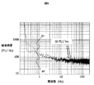
図9は、本発明の実施例の磁場計測装置を用いて測定された、ACバイアス時の磁場感度特性を示す図である。 FIG. 9 is a diagram showing magnetic field sensitivity characteristics at the time of AC bias, measured using the magnetic field measurement apparatus according to the embodiment of the present invention.
図9は、図8に示した方法を用いてACバイアス法を行い計測された磁場感度曲線91、91’のスペクトル特性を示している。図8では、2チャンネルの波形を示しており、図9中で矢印で示すように、お互いにクロストークなく20Hz近傍で50fT/√Hzを実現していることが分かる。 FIG. 9 shows the spectral characteristics of the magnetic field sensitivity curves 91 and 91 'measured by the AC bias method using the method shown in FIG. FIG. 8 shows a waveform of two channels, and it can be seen that 50 fT / √Hz is realized in the vicinity of 20 Hz without crosstalk with each other, as indicated by arrows in FIG. 9.
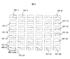
図10は、本発明の実施例の磁場計測装置を用いて、6×6のマトリックス状に配置した高温超電導SQUIDマグネットメーターによって測定された心臓磁場波形例を示す図である。 FIG. 10 is a diagram showing an example of a cardiac magnetic field waveform measured by a high-temperature superconducting SQUID magnetometer arranged in a 6 × 6 matrix using the magnetic field measurement apparatus according to the embodiment of the present invention.
図10では、高温超電導SQUIDのマグネットメーターを6×6配置して、測定した心磁図波形(101−1、101−2、〜、101−36)を約100回平均して各測定CHの位置に配置して示している。1CHから36CHの全CHで心電図信号とほぼ同じ波形が検出されていることが分かる。なお、図10において、縦軸のフルスケールは400pT、横軸のフルスケールは800msecである。 In FIG. 10, 6 × 6 magnetometers of high-temperature superconducting SQUID are arranged, and the measured magnetocardiogram waveforms (101-1, 101-2,..., 101-36) are averaged about 100 times and the position of each measurement CH. It is arranged and shown. It can be seen that almost the same waveform as the electrocardiogram signal is detected in all the channels from 1CH to 36CH. In FIG. 10, the full scale on the vertical axis is 400 pT, and the full scale on the horizontal axis is 800 msec.
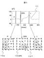
図11は、図10の磁場分布から計算された電流分布図を示す図である。 FIG. 11 is a diagram showing a current distribution diagram calculated from the magnetic field distribution of FIG.
図11では、図10で測定された磁場分布を用いて電流分布表示を行なっている。図11では、1chの波形111のP波、QRS波、T波の最大点の時点における電流分布図112−p、112−QRS、112−Tを示している。図11の電流分布図は、測定された磁場Bzから、Ix=dBz/dy、Iy=−dBz/dxにより、電流Ix、Iyを計算して求めている。なお、xy面は生体の胸部面に平行な面であり、z軸方向はxy面に垂直である。
In FIG. 11, the current distribution is displayed using the magnetic field distribution measured in FIG. FIG. 11 shows current distribution diagrams 112-p, 112-QRS, and 112-T at the time of the maximum point of the P wave, QRS wave, and T wave of the
以上のように、本発明の磁場計測装置によれば、複数のSQUID磁束計を安定にACバイアス動作させた状態で、自動で測定条件の調整が行なえ、各CH間のクロストーク無くSQUID磁束計を動作させることが可能である。 As described above, according to the magnetic field measurement apparatus of the present invention, the measurement conditions can be automatically adjusted in a state where a plurality of SQUID magnetometers are stably operated with an AC bias, and the SQUID magnetometer without crosstalk between the channels. Can be operated.
1…磁気シールドルーム、2、2−1、2−2、〜、2−N…プリアンプ部、3…クライオスタット、3−1、3−2、〜、3−N…低温部、4…ガントリー、5…被験者、6…ベッド、7、7−1、7−2、〜、7−N…駆動回路、8…アンプ・フィルター回路、9…ADコンバーター、10…インターフェースボード、11…コンピューター、12…SQUID、13…発振器、131…電流バイアス、121…外部Φext信号、132…出力電圧Vout、14…電流バイアスプラス側のV−Φ特性、15…電流バイアスマイナス側のV−Φ特性、91、91’…磁場感度曲線、101−1〜101−36…心臓磁場波形、111…心臓磁場波形、112−p…P波における電流分布図、112−QRS…QRS波における電流分布図、112−T…T波における電流分布図、SW0、SW1、SW2、SW3、SW4、SW5…スイッチ、DA0、DA1、DA2、DA3、DA4…DAコンバーター、F1…フィードバックコイル、F2…フィードバック抵抗、Vout1〜VoutN…出力信号、ΔVp…電流バイアスプラス側の変調電圧、ΔVm…電流バイアスマイナス側の変調電圧、Vmp…電流バイアスプラス側のキャンセル電圧、Vmm…電流バイアスマイナス側のキャンセル電圧、Φb…磁束の位相差。
DESCRIPTION OF
Claims (5)
4. The magnetic field measurement apparatus according to claim 3, further comprising means for obtaining a phase difference that maximizes a low frequency component of a power spectrum of a V-Φ characteristic measured when the AC bias current is applied. apparatus.
Priority Applications (1)
| Application Number | Priority Date | Filing Date | Title |
|---|---|---|---|
| JP2004111908A JP3715303B2 (en) | 2004-04-06 | 2004-04-06 | Magnetic field measuring device |
Applications Claiming Priority (1)
| Application Number | Priority Date | Filing Date | Title |
|---|---|---|---|
| JP2004111908A JP3715303B2 (en) | 2004-04-06 | 2004-04-06 | Magnetic field measuring device |
Publications (2)
| Publication Number | Publication Date |
|---|---|
| JP2005296030A true JP2005296030A (en) | 2005-10-27 |
| JP3715303B2 JP3715303B2 (en) | 2005-11-09 |
Family
ID=35328314
Family Applications (1)
| Application Number | Title | Priority Date | Filing Date |
|---|---|---|---|
| JP2004111908A Expired - Fee Related JP3715303B2 (en) | 2004-04-06 | 2004-04-06 | Magnetic field measuring device |
Country Status (1)
| Country | Link |
|---|---|
| JP (1) | JP3715303B2 (en) |
Cited By (3)
| Publication number | Priority date | Publication date | Assignee | Title |
|---|---|---|---|---|
| CN106793979A (en) * | 2014-08-28 | 2017-05-31 | 日立麦克赛尔株式会社 | Motor function evaluation system and motor function measurement device |
| JP2021060396A (en) * | 2019-10-08 | 2021-04-15 | 株式会社リコー | Magnetic field measuring device, and method for calculating magnetic flux quantum |
| US11435416B2 (en) | 2019-10-30 | 2022-09-06 | Ricoh Company, Ltd. | Magnetic field measuring apparatus |
-
2004
- 2004-04-06 JP JP2004111908A patent/JP3715303B2/en not_active Expired - Fee Related
Cited By (3)
| Publication number | Priority date | Publication date | Assignee | Title |
|---|---|---|---|---|
| CN106793979A (en) * | 2014-08-28 | 2017-05-31 | 日立麦克赛尔株式会社 | Motor function evaluation system and motor function measurement device |
| JP2021060396A (en) * | 2019-10-08 | 2021-04-15 | 株式会社リコー | Magnetic field measuring device, and method for calculating magnetic flux quantum |
| US11435416B2 (en) | 2019-10-30 | 2022-09-06 | Ricoh Company, Ltd. | Magnetic field measuring apparatus |
Also Published As
| Publication number | Publication date |
|---|---|
| JP3715303B2 (en) | 2005-11-09 |
Similar Documents
| Publication | Publication Date | Title |
|---|---|---|
| Iivanainen et al. | On-scalp MEG system utilizing an actively shielded array of optically-pumped magnetometers | |
| US5152288A (en) | Apparatus and method for measuring weak, location-dependent and time-dependent magnetic fields | |
| Wei et al. | Nested magnetic field compensation with regulated coefficients for bio-magnetic field measurement | |
| JP3473210B2 (en) | Biomagnetic measurement device | |
| JP4263544B2 (en) | Magnetic field measuring device | |
| CN112450935B (en) | A method and system for measuring magnetocardiac based on unshielded atomic magnetometer | |
| JP6890484B2 (en) | Magnetic field measuring device and measured magnetic field display method | |
| RU2504794C2 (en) | Digital amplifier with control using direct and feedback links | |
| US10641858B2 (en) | Spatiotemporal magnetic field monitoring with hall effect sensors during the MRI scan | |
| Reermann et al. | Real-time biomagnetic signal processing for uncooled magnetometers in cardiology | |
| Han et al. | Giant magneto-impedance sensor with working point selfadaptation for unshielded human bio-magnetic detection | |
| JP3715303B2 (en) | Magnetic field measuring device | |
| JP3789024B2 (en) | SQUID magnetometer | |
| US11604236B2 (en) | Optimal methods to feedback control and estimate magnetic fields to enable a neural detection system to measure magnetic fields from the brain | |
| Skidchenko et al. | The tale of two rooms: comparison of QuSpin zero-field OPMs’ operation in two magnetically shielded environments | |
| JP3949237B2 (en) | Current source estimation device | |
| JP2006518242A (en) | Compensation of magnetic field disturbance due to vibration of MRI system | |
| JPH1189817A (en) | Magnetic resonance imaging equipment | |
| JP3651540B2 (en) | Biomagnetic field measurement device | |
| EP3318887B1 (en) | A device and a method for correcting the current in a gradient coil of a magnetic resonance imaging apparatus for the compensation of the effect of eddy currents | |
| JP4427122B2 (en) | SQUID magnetometer | |
| JP3187092B2 (en) | Nuclear spin tomograph | |
| Władziński et al. | Active Compensation for OPM-MEG Inside a Two-Layer Magnetically Shielded Room | |
| CA2379800A1 (en) | Method and device for measuring biomagnetic and in particular cardiomagnetic fields | |
| JPH09192116A (en) | Nuclear magnetic resonance inspection system |
Legal Events
| Date | Code | Title | Description |
|---|---|---|---|
| TRDD | Decision of grant or rejection written | ||
| A01 | Written decision to grant a patent or to grant a registration (utility model) |
Free format text: JAPANESE INTERMEDIATE CODE: A01 Effective date: 20050816 |
|
| A61 | First payment of annual fees (during grant procedure) |
Free format text: JAPANESE INTERMEDIATE CODE: A61 Effective date: 20050824 |
|
| R150 | Certificate of patent or registration of utility model |
Ref document number: 3715303 Country of ref document: JP Free format text: JAPANESE INTERMEDIATE CODE: R150 Free format text: JAPANESE INTERMEDIATE CODE: R150 |
|
| FPAY | Renewal fee payment (event date is renewal date of database) |
Free format text: PAYMENT UNTIL: 20080902 Year of fee payment: 3 |
|
| FPAY | Renewal fee payment (event date is renewal date of database) |
Free format text: PAYMENT UNTIL: 20090902 Year of fee payment: 4 |
|
| FPAY | Renewal fee payment (event date is renewal date of database) |
Free format text: PAYMENT UNTIL: 20090902 Year of fee payment: 4 |
|
| FPAY | Renewal fee payment (event date is renewal date of database) |
Free format text: PAYMENT UNTIL: 20100902 Year of fee payment: 5 |
|
| FPAY | Renewal fee payment (event date is renewal date of database) |
Free format text: PAYMENT UNTIL: 20110902 Year of fee payment: 6 |
|
| FPAY | Renewal fee payment (event date is renewal date of database) |
Free format text: PAYMENT UNTIL: 20120902 Year of fee payment: 7 |
|
| FPAY | Renewal fee payment (event date is renewal date of database) |
Free format text: PAYMENT UNTIL: 20130902 Year of fee payment: 8 |
|
| LAPS | Cancellation because of no payment of annual fees |