JP2005295650A - Switching power supply - Google Patents
Switching power supply Download PDFInfo
- Publication number
- JP2005295650A JP2005295650A JP2004105167A JP2004105167A JP2005295650A JP 2005295650 A JP2005295650 A JP 2005295650A JP 2004105167 A JP2004105167 A JP 2004105167A JP 2004105167 A JP2004105167 A JP 2004105167A JP 2005295650 A JP2005295650 A JP 2005295650A
- Authority
- JP
- Japan
- Prior art keywords
- switching
- side circuit
- circuit
- current
- coupling capacitor
- Prior art date
- Legal status (The legal status is an assumption and is not a legal conclusion. Google has not performed a legal analysis and makes no representation as to the accuracy of the status listed.)
- Granted
Links
Images
Landscapes
- Dc-Dc Converters (AREA)
Abstract
Description
本発明は、種々の電子機器の直流電源として広く利用されるスイッチング電源装置に関するものであり、一次側回路と二次側回路の双方間で絶縁と電圧変換とを必要とするスイッチング電源装置に関するものである。
に関する。
The present invention relates to a switching power supply widely used as a DC power supply for various electronic devices, and more particularly to a switching power supply that requires insulation and voltage conversion between a primary circuit and a secondary circuit. It is.
About.
一般に、この種のスイッチング電源装置は、一次側回路と二次側回路との間の絶縁を図りつつ、一次側回路から二次側回路への電力伝送を達成する手段として、絶縁トランスが用いられている。 In general, this type of switching power supply device uses an isolation transformer as a means for achieving power transmission from the primary side circuit to the secondary side circuit while achieving insulation between the primary side circuit and the secondary side circuit. ing.
図3は、従来の1石フォワード式スイッチング電源装置の回路図で、これは例えば特許文献1などにおいて知られている。同図において、101は一次側と二次側とを絶縁するトランスで、これは周知のように一次巻線102Aと二次巻線102Bとを磁性材料であるコアで磁気結合して構成される。またトランス101の一次側において、104は商用電源、105は商用電源104からの交流電圧を全波整流する全波整流回路であり、この全波整流回路105により直流入力電圧Vinを供給する直流電源が構成されると共に、当該直流入力電圧Vinが入力コンデンサ108で平滑される。さらに、前記一次巻線102Aの正極側端子には全波整流回路104より出力される直流入力電圧Vinの正極側ラインが接続されると共に、一次巻線102Aの負極側端子にはMOS型FETであるスイッチング素子103のドレインが接続される。このスイッチング素子103およびトランス101の一次巻線102Aからなる直列回路は、直流入力電源104ひいては入力コンデンサ108の両端間に接続される。
FIG. 3 is a circuit diagram of a conventional one-stone forward switching power supply device, which is known, for example, in Patent Document 1. In the figure,
一方、トランス101の二次側回路には、二次巻線102Bの正極側端子に整流素子としてのダイオード111のアノードを接続する一方で、二次巻線102Bの負極側端子に還流素子としての別なダイオード112のアノードを接続し、これらのダイオード111,112のカソードをチョークコイル113の一端に接続すると共に、このチョークコイル113の他端とダイオード112のアノードとの間に平滑コンデンサ114を接続した出力回路115が設けられ、平滑コンデンサ114の両端には、負荷117に直流出力電圧Voを供給する出力端子121,122が接続される。この回路構成において、トランス102の一次巻線102Aに直列に接続されたスイッチング素子103がスイッチング動作を行い、全波整流回路104からの直流入力Vinを一次巻線102Aに断続的に印加すると、トランス102の二次巻線102Bに誘起した電圧が出力回路115で整流平滑され、これにより平滑コンデンサ114の両端間に発生する出力電圧Voを、出力端子121,122から負荷117に供給するようになっている。
On the other hand, in the secondary side circuit of the
また、これとは別に、出力電圧Voを安定化させる帰還ループとして、当該出力電圧Voを検出して基準電圧と比較をして、その電圧誤差を増幅する検出回路150と、この検出回路150で得られた誤差信号をトランス101の一次側回路へフィードバックする絶縁伝送素子としてのフォト・カプラ151と、この誤差信号を受けて、スイッチング素子103へのパルス駆動信号の導通幅を制御する制御回路152とをそれぞれ備えている。この制御回路152の動作により、出力電圧Voが上昇した場合は、スイッチング素子103のゲートへのパルス駆動信号の導通幅を狭くし、逆に出力電圧Voが低下した場合には、このパルス駆動信号の導通幅を広くすることにより、出力電圧Voの安定化を図ることができる。
In addition, as a feedback loop that stabilizes the output voltage Vo, a
このように、上記の回路構成においてトランス101の果たす役割は、一次側回路と二次側回路との電圧の相違を電気的に絶縁して、安全を確保すること、および、一次側回路から二次側回路へ電圧変換を行うことにある。
上述のスイッチング電源装置において、従来から使用されてきたトランス101は、一次側回路と二次側回路との電気的絶縁と電圧変換としての便利な機能を有するが、一方で次のような問題点を抱えている。
In the above-described switching power supply device, the
第一に、トランス101の損失が電源装置の損失に占める割合が大きいという問題である。トランス101はそもそも磁気の発生によりその機能が果たされるため、リーケージ・インダクタンスの発生、渦電流の発生に起因する鉄損の発生、近接効果・表皮効果等に原因する巻線中の銅損の増大等により、電源装置としての効率向上を障害している。また、効率が良くないことは、電源装置内部での発生損失が大きくなることから、この損失による発熱量が大となり、冷却強化の必要性につながる。これは、後述するコスト高の問題や寸法・重量の増大をもたらす問題の原因にもつながる。
The first problem is that the loss of the
第二に、コスト高となる問題である。すなわちトランス101の構造は、磁気鉄心に銅線などの一次巻線102Aや二次巻線102Bなどを設けたものであるので、スイッチング電源装置中の他の素子と比較して、構造が複雑であり、製作コストが高い。また、他の素子、例えば半導体素子等に比較して、実装困難な形状・構造を有するために、自動化ライン向きでなく、回路基板への実装工数の増大を招く結果となる。
The second problem is high costs. That is, the structure of the
第三に、電源装置全体としての寸法・重量の増大をもたらす問題である。磁気鉄心、銅線などで構成されるトランス101の寸法・重量は、スイッチング電源装置中の大きな部分を占めるため、電源装置全体の小形・軽量化を困難にしている。この結果、電源装置として各種の電子機器の中に組み込まれて使用される場合、電子機器中に占める空間が大となる上、重量の増加にもつながり電子機器全体の小形・軽量化の阻害要因となる。
The third problem is an increase in the size and weight of the power supply device as a whole. The size and weight of the
第四に、電磁波を発生するのでEMIの発生に関与し、このEMIの解決を困難にしている問題である。 Fourth, since electromagnetic waves are generated, it is involved in the generation of EMI and makes it difficult to solve this EMI.
本発明は上記の課題に着目してなされたもので、絶縁トランスを用いることによる種々の問題を排除して、一次側回路と二次側回路との間を絶縁した状態で電力変換を行なうことができるスイッチング電源装置を提供することをその目的とする。 The present invention has been made paying attention to the above problems, and eliminates various problems caused by using an insulating transformer, and performs power conversion in a state where the primary side circuit and the secondary side circuit are insulated. It is an object of the present invention to provide a switching power supply device that can perform the following.
請求項1の発明は、入力電圧が供給されるスイッチング手段を備えた一次側回路と、出力電圧を供給する二次側回路と、前記一次側回路と前記二次側回路との間を絶縁しつつ、前記一次側回路から前記二次側回路への電力伝送を行なう電力伝送手段とを備えたスイッチング電源装置において、前記電力伝送手段は、前記一次側回路と前記二次側回路との間に結合され、前記スイッチング手段のスイッチングにより前記二次側回路にパルス電流のみを通過させるカップリング・コンデンサにより構成されることを特徴とする。 The invention of claim 1 insulates between a primary side circuit having a switching means to which an input voltage is supplied, a secondary side circuit for supplying an output voltage, and the primary side circuit and the secondary side circuit. On the other hand, in a switching power supply device comprising power transmission means for performing power transmission from the primary side circuit to the secondary side circuit, the power transmission means is provided between the primary side circuit and the secondary side circuit. And a coupling capacitor that is coupled and allows only a pulse current to pass through the secondary circuit by switching of the switching means.
この場合、従来の絶縁トランスそのものを除去し、代わりにカップリング・コンデンサを介して一次側回路と二次側回路を結合させ、当該カップリング・コンデンサによる直流電流の遮断性能を利用して、一次側回路と二次側回路との間を直流電流に対して絶縁すると共に、スイッチング手段のスイッチングによりパルス脈動電流のみ二次側回路に通過させ、電力伝送を行なう。これにより、絶縁トランスの使用時と同等な一次側回路と二次側回路の絶縁特性を確保すると共に、二次側回路への高効率の電力供給が可能になる。 In this case, the conventional isolation transformer itself is removed, and instead the primary side circuit and the secondary side circuit are coupled via a coupling capacitor, and the primary current is cut off by the coupling capacitor. The side circuit and the secondary side circuit are insulated from the direct current, and only the pulse pulsating current is passed through the secondary side circuit by switching of the switching means to perform power transmission. As a result, it is possible to ensure the insulation characteristics of the primary side circuit and the secondary side circuit equivalent to those when the insulating transformer is used, and to supply power to the secondary side circuit with high efficiency.
請求項2の発明では、前記一次側回路は、前記入力電圧を分圧する2個の分圧素子と、この分圧素子の両端間に接続され、前記スイッチング手段を構成する直列接続された第一スイッチング素子および第二スイッチング素子とからなり、前記カップリング・コンデンサは、前記2個の分圧素子の接続点に一端を接続した第一カップリング・コンデンサと、前記第一スイッチング素子および第二スイッチング素子の接続点に一端を接続した第二カップリング・コンデンサとからなり、前記二次側回路は、前記第一カップリング・コンデンサの他端と第二カップリング・コンデンサの他端との間に接続した還流素子を備え、前記還流素子の両端間に発生する電圧を平滑して負荷に供給する構成としている。 According to a second aspect of the present invention, the primary circuit includes two voltage dividing elements that divide the input voltage, and a first connected in series that is connected between both ends of the voltage dividing element and constitutes the switching means. The coupling capacitor includes a first coupling capacitor having one end connected to a connection point of the two voltage dividing elements, the first switching element, and the second switching element. A second coupling capacitor having one end connected to a connection point of the element, and the secondary circuit is between the other end of the first coupling capacitor and the other end of the second coupling capacitor. A connected reflux element is provided, and a voltage generated between both ends of the reflux element is smoothed and supplied to a load.
このようにすると、第一スイッチング素子と第二スイッチング素子が交互にオン,オフ動作を繰返すことで、還流素子の導通時には第一カップリング・コンデンサおよび第二カップリング・コンデンサを充電し、還流素子の非導通時には第一カップリング・コンデンサおよび第二カップリング・コンデンサからの放電電流によって二次側回路に電力伝送が行なわれるようになり、二次側回路に効率よく電力を伝送することができる。 In this case, the first switching element and the second switching element are alternately turned on and off alternately, so that the first coupling capacitor and the second coupling capacitor are charged when the reflux element is turned on. When non-conducting, power is transmitted to the secondary circuit by the discharge current from the first coupling capacitor and the second coupling capacitor, and power can be efficiently transmitted to the secondary circuit. .
請求項3の発明では、前記第一カップリング・コンデンサまたは第二カップリング・コンデンサにインダクタを直列に接続している。 According to a third aspect of the present invention, an inductor is connected in series to the first coupling capacitor or the second coupling capacitor.
このようなインダクタを設けることで、そのインダクタンスにより第二スイッチング素子のオン時における電流を抑制することができる。 By providing such an inductor, the current when the second switching element is on can be suppressed by the inductance.
請求項1のスイッチング電源装置によれば、上記問題を有する絶縁トランスを排除した構成であるので、この絶縁トランスが抱える問題点が消失する。すなわち、トランスに比較してコンデンサのコストは低い上に、回路基盤への実装が容易であるので電源装置の全体コストの低減が可能となる。また、絶縁トランスの磁性部品がなくなって、電力伝送手段としての損失は、カップリング・コンデンサの導通損のみとなり、損失を低減できる。そのため、電力の効率向上が省エネルギー時代の要請にも合致する。さらに、磁気の発生が無いので、EMI対策はスイッチングによるパルス発生に原因するものに限定でき、対策に要する技術・装置が簡単になりEMI対策の好結果が得られると共に、コスト低減が実現できる。しかも、発熱量が低減するので冷却装置を小形・簡素化でき、前記の寸法・重量が低減されることと相俟って、本装置を利用する電子機器の小形・軽量化を達成することが容易となる。以上のように、請求項1の発明では、絶縁トランスを用いることによる種々の問題を排除して、一次側回路と二次側回路との間を絶縁した状態で電力変換を行なうことができる。 According to the switching power supply device of the first aspect, since the insulation transformer having the above problem is excluded, the problems of the insulation transformer disappear. In other words, the cost of the capacitor is lower than that of the transformer, and since it can be easily mounted on the circuit board, the overall cost of the power supply device can be reduced. Further, since the magnetic component of the insulating transformer is eliminated, the loss as the power transmission means is only the conduction loss of the coupling capacitor, and the loss can be reduced. Therefore, the improvement in power efficiency meets the requirements of the energy saving era. Furthermore, since there is no generation of magnetism, EMI countermeasures can be limited to those caused by pulse generation by switching, the technology and apparatus required for the countermeasures can be simplified, good results of EMI countermeasures can be obtained, and cost reduction can be realized. In addition, since the heat generation amount is reduced, the cooling device can be made smaller and simpler, and in combination with the reduction in the size and weight, the electronic device using this device can be made smaller and lighter. It becomes easy. As described above, according to the first aspect of the present invention, it is possible to perform power conversion in a state where the primary side circuit and the secondary side circuit are insulated while eliminating various problems caused by using the insulating transformer.
請求項2のスイッチング電源装置によれば、第一スイッチング素子と第二スイッチング素子が交互にオン,オフ動作を繰返すことで、第一カップリング・コンデンサおよび第二カップリング・コンデンサを充放電でき、二次側回路に効率よく電力を伝送することができる。 According to the switching power supply device of claim 2, the first coupling capacitor and the second coupling capacitor can be charged / discharged by alternately repeating the on / off operation of the first switching element and the second switching element, Electric power can be efficiently transmitted to the secondary side circuit.
請求項3のスイッチング電源装置によれば、第二スイッチング素子のオン時における電流を、単独の素子で抑制することができる。 According to the switching power supply device of the third aspect, the current when the second switching element is on can be suppressed by a single element.
以下、本発明におけるスイッチング電源装置の好ましい実施形態について、添付図面である図1と図2を参照して詳細に説明する。 Hereinafter, a preferred embodiment of a switching power supply device according to the present invention will be described in detail with reference to FIGS. 1 and 2 which are attached drawings.
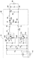
回路の全体構成を示す図1において、ここでは一点差線で区切られた符号31を一次側回路とし、同様に別に区切られた32を二次側回路とする。一次側回路31は後述するコンデンサ18,19の前段にあって、直流入力電圧Vinが印加される回路であり、二次側回路32はコンデンサ18,19の後段にあって、直流出力電圧Voを出力する回路をいう。
In FIG. 1 showing the overall configuration of the circuit, here,
一次側回路31の構成を説明すると、11は交流電源10からの交流電圧を整流する直流電源としての全波整流回路、12はこの全波整流回路11の両端に接続する入力コンデンサで、全波整流回路11からの直流入力電圧Vinが入力コンデンサ12で平滑されるようになっている。また、全波整流回路11ひいては入力コンデンサ12の両端間には、いずれもMOS型FETを使用した第一スイッチング素子16と第二スイッチング素子17との直列回路が接続される。ここでは、第一スイッチング素子16のソースに第二スイッチング素子17のドレインが接続され、第一スイッチング素子16のドレインは全波整流回路11の正極側に、第二スイッチング素子17のソースが全波整流回路11の負極側にそれぞれ接続される。また、直流入力電圧Vinを分割するためのコンデンサ13,14がスイッチング素子16,17の直列回路の両端間に接続され、コンデンサ13,14の接続点には第二のカップリング・コンデンサ19の一端が接続される。そして、インダクタ15の一方の端子が第一スイッチング素子16のソースと第二スイッチング素子17のドレインとの接続点に接続されると共に、インダクタ15の他方の端子がカップリング・コンデンサ18の一端に接続される。また、第一スイッチング素子16と第二スイッチング素子17には、それぞれ各ソースとドレイン間の浮遊容量としての寄生キャパシタンス16C,17Cが存在すると共に、内蔵するボディー・ダイオード16D,17Dが存在する。以上が、一次側回路31の構成である。
The configuration of the
さて、カップリング・コンデンサ18,19の各他端は二次側回路32に結合され、2個のカップリング・コンデンサ18,19により、一次側回路31の直流入力電源を二次側に対して絶縁する。すなわち、カップリング・コンデンサ18の他端には、還流ダイオード20のカソードとダイオード21のアノードに接続され、この還流ダイオード20のアノードがカップリング・コンデンサ19の他端に接続されると共に、ダイオード21のカソードがチョークコイル22の一端に接続され、チョークコイル22の他端が平滑コンデンサ23の一端が接続され、さらにこの平滑コンデンサ23の他端が前記カップリング・コンデンサ19の他端と還流ダイオード20との接続点に接続される。そして、平滑コンデンサ23の両端にそれぞれ出力端子24,25を接続して、この出力端子24,25間に発生する直流出力電圧Voを負荷26に供給する。以上が二次側回路32の構成である。
The other ends of the
以上説明したように、上記図1における回路では、一次側回路31から二次側回路32への電力変換手段として絶縁トランスは用いられておらず、代わりにカップリング・コンデンサ18,19により、一次側回路31から二次側回路32への電力伝送および直流絶縁がなされる構成を有する。
As described above, the circuit in FIG. 1 does not use an insulating transformer as a power conversion means from the
なお、ここには図示しないが、出力電圧Voを安定化させる帰還ループとして、従来例で示す検出回路150およびフォト・カプラ151と、このフォト・カプラ151からの誤差信号を受けて、第一スイッチング素子16と第二スイッチング素子17へのパルス駆動信号の導通幅を制御する制御回路152がそれぞれ設けられる。但し、ここでの制御回路152は、第一スイッチング素子16と第二スイッチング素子17を交互にオン・オフ動作させるパルス駆動信号を出力する。
Although not shown here, as a feedback loop for stabilizing the output voltage Vo, the
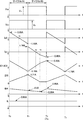
次に上記の回路について、シミュレーションを行った結果に基づきその動作状態を、回路図を示す図1と各部の波形を示す図2とにより詳しく説明する。 Next, the operation state of the above circuit will be described in detail with reference to FIG. 1 showing a circuit diagram and FIG. 2 showing waveforms of each part based on the result of simulation.
ここで先ず、各部を流れる電流を定義すると、Iq1は第一スイッチング素子16を流れる電流、Iq2は第二スイッチング素子17を流れる電流、IC1はカップリング・コンデンサ18を流れる電流、IC2はカップリング・コンデンサ19を流れる電流、ID3は還流ダイオード20を流れる電流、ID4はダイオード21を流れる電流、ILは負荷26を流れる電流(負荷電流)で、夫々の電流の方向が図1に示す矢印の方向に流れる場合を正の方向とする。また図2には、これらの各電流Iq2,Iq1,IC1(=IC2),ID3,ID4,ILの波形と共に、第一スイッチング素子17のソース・ドレイン間電圧VQ2と、第一スイッチング素子17のソース・ドレイン間電圧VQ1をそれぞれ示している。また、図1に示す二次側回路32の構成から明らかなように、ID4=IC1+ID3となっており、負荷電流ILは、チョークコイル22と平滑コンデンサ23により電流ID4が平滑されて、脈動が除かれた一定な直流電流となる。また、カップリング・コンデンサ18,19の極性は、図1に示すドット(・)側すなわちカップリング・コンデンサ18,19への充電電流IC1,IC2が流れ込む側を正極とする。従って、第二カップリング・コンデンサ18は一次側回路31側が、第一カップリング・コンデンサ19は二次側回路32側が正極となる。
First, when the current flowing through each part is defined, Iq1 is the current flowing through the
この回路構成では、インダクタ15とカップリング・コンデンサ18,19の直列回路とからなるLC回路により共振電流が流れ、各電流は回路定数で決まる共振条件によりその流れる向きを反転する。今、入力コンデンサ12の両端間に発生する直流入力電圧Vin=100Vとして、一次側回路31や二次側回路32を構成する各素子の静電容量やインダクタンスを所定の値に設定し、所定の負荷26を出力端子24,25の両端間に接続して、各スイッチング素子16,17を例えば5MHzのスイッチング周波数で動作させた場合をシミュレーションした結果について、図2の各部の波形図を参照しながら説明する。
In this circuit configuration, a resonance current flows through an LC circuit including an
先ず、第一スイッチング素子16がオフし、第二スイッチング素子17がオンする時間T0の直前において、第一スイッチング素子16を流れる電流Iq1は負の方向に流れる一方で、カップリング・コンデンサ18,19には充電電流IC1,IC2が正方向に流れているが、チョークコイル22はカップリング・コンデンサ18からの充電電流IC1により磁気エネルギーを蓄積中であり、還流ダイオード20におけるチョークコイル22のエネルギーを還流する電流ID3はゼロになっている。すなわち、ダイオード21を介してチョークコイル22に流れ込む電流ID4と前記充電電流IC1は等しく、このチョークコイル22に流れ込む電流ID4により負荷電流ILを供給している。
First, immediately before the time T0 when the
次に時間T0の直後においては、第一スイッチング素子16がオフしてその両端間電圧VQ1がゼロになる一方で、第二スイッチング素子17はオンしてその両端間電圧VQ2が入力電圧Vinになる。ここでは、電圧分割用のコンデンサ14の正極側→カップリング・コンデンサ19→還流ダイオード20→カップリング・コンデンサ18→インダクタ15→第二スイッチング素子17→コンデンサ14の負極側からなる第1の閉回路が形成されると共に、もう一つ、チョークコイル22→負荷26→還流ダイオード20→ダイオード21→チョークコイル22からなる第2の閉回路が存在する。時間T0の直前に、第一スイッチング素子16を介して負の方向に電流Iq1が流れていた関係で、時間T0の直後には、この電流Iq1の連続性を維持するために、第二スイッチング素子17に正方向の電流Iq2が立ち上がり、第一スイッチング素子16を流れる電流はゼロとなる。この時点で、Iq2,IC1,IC2の各電流値は、時間T0の直前におけるIq1の電流値と等しく0.95Aとなり、還流ダイオード20を流れる電流ID3は0Aである。従って、ダイオード21を介してチョークコイル22に流れ込む電流ID4は、ID4=IC1+ID3=0.95Aとなる。カップリング・コンデンサ18,19の電流IC1,IC2は、第二スイッチング素子17に流れる電流Iq2と反対の方向、すなわち未だ充電方向に流れているが、この電流IC1,IC2は充電が進むにつれて減少する。また電流Iq2も、カップリング・コンデンサ18の充電が進行するに連れて、電流IC1,IC2と同一の勾配で減少する。
Next, immediately after time T0, the
やがて、図2に示す時間t1になると、LC共振によりこれらの電流IC1,IC2,Iq2はその流れる方向を反転する。すなわち、両カップリング・コンデンサ18、19が満充電になると今度は放電に転じ、電流IC1,IC2はその方向を負方向に反転して、放電を開始する。すると、第二スイッチング素子17に流れる電流Iq2は両カップリング・コンデンサ18,19を充電すべく、その方向を同じく反転する。一方、別の第2の閉回路においては、時間Toの直後からチョークコイル22の放電が始まり、還流ダイオード20を通じて電流ID3を流し、その値を徐々に増加させる。以上の、各電流変化により、このサイクルの終了時間T1においては、Iq2,IC1,IC2=−1.16A、ID3=1.71Aとなり、この結果、漸減する電流ID4=IC1+ID3=1.71−1.16=0.55Aとなる。この電流ID4が平滑コンデンサ23により平滑された直流電流ILが負荷26へ流れ、時間T0からT1までのスイッチング・サイクル(A)を終了する。
Eventually, at time t1 shown in FIG. 2, the currents IC1, IC2, and Iq2 reverse their flow directions due to LC resonance. That is, when both the
次に、スイッチング・サイクル(B)の開始となる時間T1になると、第一スイッチング素子16がオンしてその両端間電圧VQ1が入力電圧Vinになる一方で、第二スイッチング素子17はオフしてその両端間電圧VQ2がゼロになる。この時間T1の直後には、電圧分割用のコンデンサ13の正極側→スイッチング素子16→インダクタ15→カップリング・コンデンサ18→ダイオード20→チョークコイル22→負荷26→カップリング・コンデンサ19→コンデンサ13からなる第3の閉回路と、もう一つ、チョークコイル22→負荷26→還流ダイオード20→ダイオード21→チョークコイル22からなる前述の第2の閉回路が存在する。時間T1の直前に、第二スイッチング素子17を介して負の方向に電流Iq2が流れていた関係で、時間T1の直後には、この電流Iq2の連続性を維持するために、第一スイッチング素子16に正方向の電流Iq1が立ち上がり、第二スイッチング素子17を流れる電流Iq2はゼロとなる。この電流Iq1は、前述のスイッチング・サイクル(A)でIq2により充電されていた状態をさらに受けて、両カップリング・コンデンサ18,19の充電を続け、時間T1の時点ではIq1=1.16A、IC1,IC2=−1.16A、ID3=1.71A、従って、ID4=1.71−1.16=0.55Aとなっている。電流Iq1は充電が進むと共に漸減すると共に、カップリング・コンデンサ18,19の電流IC1,IC2も、電流Iq1と同一の勾配でゼロに近づいてゆく。
Next, at time T1 when the switching cycle (B) starts, the
やがて時間t2になると、第一スイッチング素子16を流れる電流Iq1は、インダクタ15とカップリング・コンデンサ18との共振により反転する。一方、前述のスイッチング・サイクル(A)で放電していた両カップリング・コンデンサ18,19の放電電流は減少して、IC1,IC2は時間t2でゼロとなり、反転して充電に転じる。また、還流ダイオード20を流れる電流ID3は、時間t2を過ぎて時間t3までの間、電流IC1,IC2が変化するのに伴い漸減する。このT1からt3までの間、ダイオード21を介してチョークコイル22に流れ込む電流ID4は、還流ダイオード20を流れる電流ID3の減少により、スイッチング・サイクル(A)と同様な変化勾配で漸減し、時間t3でID4=0.35Aとなる。時間t3に達した時点で、チョークコイル22はその磁気エネルギーの放出を終了して、還流ダイオード20を流れる電流ID3はゼロとなり、そこからチョークコイル22の磁気エネルギーの蓄積が始まる。この結果、両カップリング・コンデンサ18,19の充電電流IC1,IC2の増加は緩やかになり、負に反転した電流Iq1の変化も緩やかになる。そして、このスイッチング・サイクル(B)の終了時における時間T2では、Iq1=0.95A、IC1,IC2=0.95A、ID3=0A、従って、ID4=0.95+0=0.95Aとなる。
Eventually, at time t2, the current Iq1 flowing through the
従って、前記チョークコイル22に流れ込む電流ID4が平滑コンデンサ23により平滑された直流電流ILとなって負荷26へ流れ、時間T1〜T2までのこのサイクル(B)を終了し、次のスイッチング・サイクル、すなわち、前記スイッチング・サイクルへ(A)へと移行する。以下、スイッチング・サイクル(A),(B)を繰り返すことで、直流出力電圧Voが6.5Vで、直流負荷電流が0.65Aである出力電力を負荷26に供給し続けることができる。
Therefore, the current ID4 flowing into the
以上述べたように、従来のトランス101をカップリング・コンデンサ18,19に置き換えた本発明によるコンデンサ結合型のスイッチング電源装置は、カップリング・コンデンサ18,19に加えられる電圧極性をスイッチングにより反転させるサイクルを繰り返すことにより、当該カップリング・コンデンサ18,19を充放電させて、負荷電流を継続して流すことが可能である。この結果、従来使用されていたトランスを省くことが可能となり、電源装置自体の小形・軽量化とそれに伴うコスト低減、この電源を利用する電子機器の小形・軽量化とそれに伴うコスト低減、EMI対策の容易化等に貢献することができる。
As described above, the capacitor-coupled switching power supply device according to the present invention in which the
以上のように本実施例では、入力電圧Vinが供給されるスイッチング手段である第一スイッチング素子16および第二スイッチング素子17を備えた一次側回路31と、出力電圧Voを供給する二次側回路32と、この一次側回路31と二次側回路32との間を絶縁しつつ、一次側回路31から二次側回路32への電力伝送を行なう電力伝送手段とを備えたスイッチング電源装置において、前記電力伝送手段は、一次側回路31と二次側回路32との間に結合され、第一スイッチング素子16および第二スイッチング素子17のスイッチングにより二次側回路32にパルス電流のみを通過させるカップリング・コンデンサ18,19により構成される。
As described above, in this embodiment, the
この場合、従来の絶縁トランス101そのものを除去し、代わりにカップリング・コンデンサ18,19を介して一次側回路31と二次側回路32を結合させ、当該カップリング・コンデンサ18,19による直流電流の遮断性能を利用して、一次側回路31と二次側回路32との間を直流電流に対して絶縁すると共に、第一スイッチング素子16および第二スイッチング素子17のスイッチングによりパルス脈動電流のみを二次側回路32に通過させ、電力伝送を行なう。これにより、絶縁トランス101の使用時と同等な一次側回路31と二次側回路32の絶縁特性を確保すると共に、二次側回路32への高効率の電力供給が可能になる。
In this case, the
そして上記構成を備えていれば、トランスに比較してコンデンサのコストは低い上に、回路基盤への実装が容易であるので、スイッチング電源装置としての全体コストの低減が可能となる。また、絶縁トランス101の磁性部品がなくなって、電力伝送手段としての損失は、カップリング・コンデンサ18,19の導通損のみとなり、損失を低減できる。そのため、電力の効率向上が省エネルギー時代の要請にも合致する。さらに、磁気の発生が無いので、EMI対策はスイッチングによるパルス発生に原因するものに限定でき、対策に要する技術・装置が簡単になりEMI対策の好結果が得られると共に、コスト低減が実現できる。しかも、発熱量が低減するので冷却装置を小形・簡素化でき、前記の寸法・重量が低減されることと相俟って、本装置を利用する電子機器の小形・軽量化を達成することが容易となる。
If the above configuration is provided, the cost of the capacitor is lower than that of the transformer and the mounting on the circuit board is easy, so that the overall cost of the switching power supply device can be reduced. Further, since the magnetic component of the insulating
また本実施例では、前記一次側回路31が、前記入力電圧Vinを分圧する2個の分圧素子としてのコンデンサ13,14と、このコンデンサ13,14の両端間に接続され、スイッチング手段を構成する直列接続された第一スイッチング素子16および第二スイッチング素子17とからなり、前記カップリング・コンデンサ18,19は、前記2個のコンデンサ13,14の接続点に一端を接続した第一カップリング・コンデンサ19と、第一スイッチング素子16および第二スイッチング素子17の接続点に一端を接続した第二カップリング・コンデンサ18とからなり、前記二次側回路32は、第一カップリング・コンデンサ19の他端と第二カップリング・コンデンサ18の他端との間に接続した還流素子としての還流ダイオード20を備え、還流ダイオード20の両端間に発生する電圧を平滑して負荷26に出力電圧Voを供給する構成としている。
In this embodiment, the
このようにすると、第一スイッチング素子16と第二スイッチング素子17が交互にオン,オフ動作を繰返すことで、還流ダイオード20の導通時には第一カップリング・コンデンサ19および第二カップリング・コンデンサ18を充電し、還流ダイオード20の非導通時には第一カップリング・コンデンサ19および第二カップリング・コンデンサ18からの放電電流によって二次側回路32に電力伝送が行なわれるようになり、二次側回路32に効率よく電力を伝送することができる。
In this way, the
さらに本実施例では、前記第一カップリング・コンデンサ19または第二カップリング・コンデンサ18にインダクタ15を直列に接続している。
Furthermore, in this embodiment, an
このようなインダクタ15を設けることで、そのインダクタンスにより第二スイッチング素子17のオン時における電流を抑制することができる。
By providing such an
なお、本発明は上記実施例に限定されるものではなく、本発明の要旨の範囲において種々の変形実施が可能である。本発明は、実施例にあるようなフォワード型のスイッチング電源装置に限定されるものではなく、従来トランスを使用してきた各種タイプのスイッチング電源装置に広く適用可能であり、前記トランスの抱える問題点の解決が可能となる。また、還流素子としては実施例中におけるダイオードに限らず、例えばMOS型FETなどのオン抵抗の小さなスイッチ素子を利用できる。 In addition, this invention is not limited to the said Example, A various deformation | transformation implementation is possible in the range of the summary of this invention. The present invention is not limited to the forward type switching power supply as in the embodiment, but can be widely applied to various types of switching power supplies that have conventionally used a transformer. A solution is possible. Further, the reflux element is not limited to the diode in the embodiment, and a switch element having a small on-resistance such as a MOS FET can be used.
13,14 コンデンサ(分圧素子)
15 インダクタ
16 第一スイッチング素子(スイッチング手段)
17 第二スイッチング素子(スイッチング手段)
18 第二カップリング・コンデンサ(カップリング・コンデンサ,電力伝送手段)
19 第一カップリング・コンデンサ(カップリング・コンデンサ,電力伝送手段)
20 還流ダイオード(還流素子)
31 一次側回路
32 二次側回路
13, 14 Capacitor (voltage divider)
15 Inductor
16 First switching element (switching means)
17 Second switching element (switching means)
18 Second coupling capacitor (coupling capacitor, power transmission means)
19 First coupling capacitor (coupling capacitor, power transmission means)
20 Reflux diode
31 Primary circuit
32 Secondary circuit
Claims (3)
前記電力伝送手段は、前記一次側回路と前記二次側回路との間に結合され、前記スイッチング手段のスイッチングにより前記二次側回路にパルス電流のみを通過させるカップリング・コンデンサにより構成されることを特徴とするスイッチング電源装置。 A primary side circuit provided with a switching means to which an input voltage is supplied, a secondary side circuit that supplies an output voltage, and the primary side circuit and the secondary side circuit are insulated from the primary side circuit while insulating between the primary side circuit and the secondary side circuit. In a switching power supply device comprising power transmission means for performing power transmission to the secondary side circuit,
The power transmission means is constituted by a coupling capacitor which is coupled between the primary side circuit and the secondary side circuit and allows only the pulse current to pass through the secondary side circuit by switching of the switching means. A switching power supply device.
前記カップリング・コンデンサは、前記2個の分圧素子の接続点に一端を接続した第一カップリング・コンデンサと、前記第一スイッチング素子および第二スイッチング素子の接続点に一端を接続した第二カップリング・コンデンサとからなり、
前記二次側回路は、前記第一カップリング・コンデンサの他端と第二カップリング・コンデンサの他端との間に接続した還流素子を備え、前記還流素子の両端間に発生する電圧を平滑して負荷に前記出力電圧を供給する構成としたことを特徴とする請求項1記載のスイッチング電源装置。 The primary side circuit includes two voltage dividing elements that divide the input voltage, and a first switching unit that is connected between both ends of the voltage dividing element and that is alternately connected in series and that constitutes the switching means. An element and a second switching element,
The coupling capacitor includes a first coupling capacitor having one end connected to a connection point of the two voltage dividing elements, and a second connection having one end connected to a connection point of the first switching element and the second switching element. Consisting of a coupling capacitor,
The secondary circuit includes a return element connected between the other end of the first coupling capacitor and the other end of the second coupling capacitor, and smoothes a voltage generated between both ends of the return element. The switching power supply device according to claim 1, wherein the output voltage is supplied to a load.
3. The switching power supply device according to claim 2, wherein an inductor is connected in series to the first coupling capacitor or the second coupling capacitor.
Priority Applications (1)
| Application Number | Priority Date | Filing Date | Title |
|---|---|---|---|
| JP2004105167A JP4366713B2 (en) | 2004-03-31 | 2004-03-31 | Switching power supply |
Applications Claiming Priority (1)
| Application Number | Priority Date | Filing Date | Title |
|---|---|---|---|
| JP2004105167A JP4366713B2 (en) | 2004-03-31 | 2004-03-31 | Switching power supply |
Publications (2)
| Publication Number | Publication Date |
|---|---|
| JP2005295650A true JP2005295650A (en) | 2005-10-20 |
| JP4366713B2 JP4366713B2 (en) | 2009-11-18 |
Family
ID=35327984
Family Applications (1)
| Application Number | Title | Priority Date | Filing Date |
|---|---|---|---|
| JP2004105167A Expired - Fee Related JP4366713B2 (en) | 2004-03-31 | 2004-03-31 | Switching power supply |
Country Status (1)
| Country | Link |
|---|---|
| JP (1) | JP4366713B2 (en) |
Families Citing this family (1)
| Publication number | Priority date | Publication date | Assignee | Title |
|---|---|---|---|---|
| JP7559759B2 (en) | 2019-08-13 | 2024-10-02 | ソニーグループ株式会社 | Power supply circuit and control method |
-
2004
- 2004-03-31 JP JP2004105167A patent/JP4366713B2/en not_active Expired - Fee Related
Also Published As
| Publication number | Publication date |
|---|---|
| JP4366713B2 (en) | 2009-11-18 |
Similar Documents
| Publication | Publication Date | Title |
|---|---|---|
| US7218534B2 (en) | Switching power supply circuit | |
| US7656686B2 (en) | Switching power supply circuit | |
| US9667153B2 (en) | Switching power supply apparatus for generating control signal for lowering switching frequency of switching devices | |
| EP2670037A1 (en) | Switching power supply device | |
| US20170155325A1 (en) | Resonant power supply device | |
| JP2015144554A (en) | Power converter | |
| JP2004274262A (en) | Electrically insulated switch element driving circuit | |
| CN106685242B (en) | Single-stage AC-DC converter | |
| TWI513164B (en) | Flyback active clamping power converter | |
| KR20180004675A (en) | Bidirectional Converter with Auxiliary LC Resonant Circuit and Operating Method thereof | |
| CN106575927B (en) | power conversion device | |
| JP2018506948A (en) | Induction power receiver | |
| US10164542B2 (en) | Electronic converter, and corresponding method for designing a magnetic component | |
| JP2018196271A (en) | Power conversion device | |
| US6909267B2 (en) | Logic controlled high voltage resonant switching power supply | |
| TWI840390B (en) | System for transferring electrical power to an electrical load | |
| JP4366713B2 (en) | Switching power supply | |
| JPWO2015178106A1 (en) | Power supply circuit | |
| KR101229265B1 (en) | Integrated transformer and high step-up dc/dc converter using the same | |
| Ozawa et al. | Implementation and evaluation of pre-and post-regulation control with class-e 2 wireless power transfer system | |
| JP3909407B2 (en) | Electrically isolated switching element drive circuit | |
| JP2006211878A (en) | Switching power unit | |
| JP4842998B2 (en) | Electromagnetic induction heating device | |
| JPH09131055A (en) | Switching regulator | |
| JP3326655B2 (en) | Current resonant switching power supply |
Legal Events
| Date | Code | Title | Description |
|---|---|---|---|
| A621 | Written request for application examination |
Free format text: JAPANESE INTERMEDIATE CODE: A621 Effective date: 20051207 |
|
| A131 | Notification of reasons for refusal |
Free format text: JAPANESE INTERMEDIATE CODE: A131 Effective date: 20090205 |
|
| A521 | Request for written amendment filed |
Free format text: JAPANESE INTERMEDIATE CODE: A523 Effective date: 20090327 |
|
| TRDD | Decision of grant or rejection written | ||
| A01 | Written decision to grant a patent or to grant a registration (utility model) |
Free format text: JAPANESE INTERMEDIATE CODE: A01 Effective date: 20090803 |
|
| A01 | Written decision to grant a patent or to grant a registration (utility model) |
Free format text: JAPANESE INTERMEDIATE CODE: A01 |
|
| A61 | First payment of annual fees (during grant procedure) |
Free format text: JAPANESE INTERMEDIATE CODE: A61 Effective date: 20090816 |
|
| R150 | Certificate of patent or registration of utility model |
Ref document number: 4366713 Country of ref document: JP Free format text: JAPANESE INTERMEDIATE CODE: R150 Free format text: JAPANESE INTERMEDIATE CODE: R150 |
|
| FPAY | Renewal fee payment (event date is renewal date of database) |
Free format text: PAYMENT UNTIL: 20120904 Year of fee payment: 3 |
|
| S531 | Written request for registration of change of domicile |
Free format text: JAPANESE INTERMEDIATE CODE: R313531 |
|
| FPAY | Renewal fee payment (event date is renewal date of database) |
Free format text: PAYMENT UNTIL: 20120904 Year of fee payment: 3 |
|
| R350 | Written notification of registration of transfer |
Free format text: JAPANESE INTERMEDIATE CODE: R350 |
|
| FPAY | Renewal fee payment (event date is renewal date of database) |
Free format text: PAYMENT UNTIL: 20130904 Year of fee payment: 4 |
|
| LAPS | Cancellation because of no payment of annual fees |