JP2005295637A - Switching power supply - Google Patents
Switching power supply Download PDFInfo
- Publication number
- JP2005295637A JP2005295637A JP2004104587A JP2004104587A JP2005295637A JP 2005295637 A JP2005295637 A JP 2005295637A JP 2004104587 A JP2004104587 A JP 2004104587A JP 2004104587 A JP2004104587 A JP 2004104587A JP 2005295637 A JP2005295637 A JP 2005295637A
- Authority
- JP
- Japan
- Prior art keywords
- switching
- frequency
- power supply
- voltage
- switching element
- Prior art date
- Legal status (The legal status is an assumption and is not a legal conclusion. Google has not performed a legal analysis and makes no representation as to the accuracy of the status listed.)
- Granted
Links
- 239000000284 extract Substances 0.000 claims description 3
- 230000003247 decreasing effect Effects 0.000 abstract description 3
- 239000012141 concentrate Substances 0.000 abstract 1
- 239000003990 capacitor Substances 0.000 description 5
- 230000007423 decrease Effects 0.000 description 5
- 238000004804 winding Methods 0.000 description 5
- 238000010586 diagram Methods 0.000 description 4
- 238000001514 detection method Methods 0.000 description 3
- 238000005259 measurement Methods 0.000 description 3
- 238000009499 grossing Methods 0.000 description 2
- 230000007257 malfunction Effects 0.000 description 2
- 238000001228 spectrum Methods 0.000 description 2
- 239000004575 stone Substances 0.000 description 2
- 238000012935 Averaging Methods 0.000 description 1
- 230000002411 adverse Effects 0.000 description 1
- 238000004891 communication Methods 0.000 description 1
- 230000000694 effects Effects 0.000 description 1
- 238000000034 method Methods 0.000 description 1
- 230000010355 oscillation Effects 0.000 description 1
- 230000000087 stabilizing effect Effects 0.000 description 1
- 230000001629 suppression Effects 0.000 description 1
- 238000003079 width control Methods 0.000 description 1
Images
Landscapes
- Dc-Dc Converters (AREA)
Abstract
Description
本発明は、スイッチング動作に伴い発生するノイズを簡単な構成で低減したスイッチング電源装置に関する。 The present invention relates to a switching power supply apparatus that reduces noise generated by a switching operation with a simple configuration.
近年、電子機器における制御周波数の激増や例えば携帯電話などの無線通信の普及から各機器相互間の電磁環境の整合性(EMC:Electro-Magnetic Compatibility)への関心が高まっている。実際、EMC対応規格としてCEマーキングなどのノイズ規格もあり、電子機器から発生するノイズを抑制するため、様々な対策がなされている。とりわけ電子機器の電源として広く用いられるスイッチング電源は、スイッチング動作に伴う強いノイズが発生することから、ノイズ発生源として他の機器の誤動作や機能停止などといった弊害を招く虞があり、ノイズ抑制が強く要求されている。 In recent years, interest in electromagnetic compatibility (EMC: Electro-Magnetic Compatibility) between devices has increased due to the rapid increase in control frequency in electronic devices and the spread of wireless communication such as mobile phones. In fact, there is a noise standard such as CE marking as an EMC-compliant standard, and various countermeasures are taken to suppress noise generated from electronic equipment. In particular, switching power supplies that are widely used as power sources for electronic devices generate strong noises associated with switching operations, which may cause adverse effects such as malfunctions or malfunctions of other devices as noise sources, and noise suppression is strong. Requested.
従来のスイッチング電源装置として、特許文献1に開示されるようなものがある。これは、商用交流電力をダイオードブリッジで全波整流し、PFC回路(Power Factor Collect)により高調波電流を抑制し、力率改善することにより直流電力とし、スイッチング素子をオン・オフ動作させることにより該直流電力から出力電圧を取り出している。このようなスイッチング電源では、入力電源に商用交流電力を用いているため、スイッチング動作時のエネルギーが大きく、スイッチング動作に伴う強いスイッチングノイズが発生する。このようなスイッチングノイズを抑制するための周知の技術として、スナバ回路,タンク回路(共振回路),各種フィルターが知られている。
しかし、上記従来のスイッチング電源装置では、スイッチング素子のスイッチング動作に伴うスイッチングノイズが発生し、前述したようなノイズ対策回路を設けても、該ノイズが効果的に抑制されないという問題があった。又、その為、フィルタ等により対策すると、大きなものが必要となり面積と労力を費やす。 However, in the above conventional switching power supply device, there is a problem that switching noise occurs due to the switching operation of the switching element, and even if the noise countermeasure circuit as described above is provided, the noise is not effectively suppressed. For this reason, if measures are taken with a filter or the like, a large one is required, and an area and labor are consumed.
そこで本発明は上記問題点に鑑み、スイッチング動作に伴い発生する基本波成分を含むノイズを簡単な構成で効果的に低減したスイッチング電源装置を提供することを目的とする。 SUMMARY OF THE INVENTION In view of the above problems, an object of the present invention is to provide a switching power supply apparatus that can effectively reduce noise including a fundamental wave component generated in association with a switching operation with a simple configuration.
本発明の請求項1におけるスイッチング電源装置では、スイッチング素子をオン・オフ動作させることにより交流電圧から出力電圧を取り出すスイッチング電源装置において、前記スイッチング素子のオン・オフ動作を制御する制御周波数を前記交流電圧の振幅に応じて変化させるスイッチング制御手段を備えるよう構成している。 In the switching power supply device according to the first aspect of the present invention, in the switching power supply device that extracts the output voltage from the AC voltage by turning on / off the switching element, the control frequency for controlling the on / off operation of the switching element is set to the AC power supply. A switching control means for changing the voltage according to the amplitude of the voltage is provided.
このようにすると、スイッチング素子のオン・オフ動作を制御する制御周波数が、交流電圧の振幅に応じて増減するため、制御周波数に揺らぎが生じる。該制御周波数に揺らぎが生じると、スイッチング周波数が一定とならず、スイッチング周波数のn倍波に対応する帯域毎に集中して発生していたノイズが、スイッチング周波数が揺らいでいる帯域幅で分散されることとなる。従って、測定帯域内でのノイズ強度のピークを周波数の振れ幅で平均化し、低減することができる。また、元々揺らぎを有する交流電圧の振幅に応じて、制御周波数を変化させるだけでよいので、簡単な構成でノイズを抑制することができる。 In this case, the control frequency for controlling the on / off operation of the switching element increases / decreases in accordance with the amplitude of the AC voltage, so that the control frequency fluctuates. When the control frequency fluctuates, the switching frequency does not become constant, and noise that is concentrated in each band corresponding to the n-th harmonic of the switching frequency is distributed over the bandwidth where the switching frequency fluctuates. The Rukoto. Therefore, the peak of the noise intensity within the measurement band can be averaged and reduced by the frequency fluctuation width. Further, since it is only necessary to change the control frequency in accordance with the amplitude of the alternating voltage originally having fluctuations, noise can be suppressed with a simple configuration.
本発明の請求項1では、簡単な構成で、スイッチング動作に伴うノイズ強度のピークを周波数振幅で平均化し、低減することができるスイッチング電源を提供することが可能になる。 According to the first aspect of the present invention, it is possible to provide a switching power supply capable of averaging and reducing the noise intensity peak accompanying the switching operation by the frequency amplitude with a simple configuration.
以下、添付図面を参照しながら、本発明におけるスイッチング電源の好ましい実施例を説明する。なお、これらの各実施例において、従来例と同一箇所には同一符号を付し、共通する部分の説明は重複するため極力省略する。 Hereinafter, preferred embodiments of a switching power supply according to the present invention will be described with reference to the accompanying drawings. Note that, in each of these embodiments, the same portions as those in the conventional example are denoted by the same reference numerals, and the description of the common parts will be omitted as much as possible.
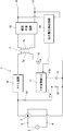
図1は本実施例におけるスイッチング電源装置の回路図を示したものである。同図において、2は例えば商用電源などの交流入力電源であり、スイッチング電源装置1の一対の入力端子3,4に接続されている。5はダイオードブリッジであり、PFC回路6に接続される。一対の入力端子3,4を介して交流入力電源2から供給される交流電圧は、ダイオードブリッジ5で全波整流され、PFC回路6で力率改善されることで、直流電圧に変換される。7は入力側と出力側とを絶縁するトランスで、一次巻線7aの一端にはPFC回路6が接続され、他端にはMOS型FETからなるスイッチング素子10のドレインが接続される。スイッチング素子10のソースはダイオードブリッジ5と接続され、ゲートはスイッチング素子10のオン・オフ動作(スイッチング動作)を制御するPWM制御IC11と接続される。PWM制御IC11には、抵抗12の一端が抵抗接続端子11aに、コンデンサ13の一端がコンデンサ接続端子11bにそれぞれ接続され、抵抗12及びコンデンサ13の他端は、スイッチング素子10のソースとダイオードブリッジ5とを繋ぐラインに接続される。スイッチング素子10のスイッチング周波数すなわちPWM制御IC11の制御周波数は、抵抗12とコンデンサ13との時定数により決定され、該時定数を変化させることにより、当該制御周波数も変化することとなる。一般的に使用されるPWM制御ICでは、コンデンサ13の値を固定とした場合、抵抗12の抵抗値を大きくすると制御周波数が低くなり、反対に、抵抗12の抵抗値を小さくすると制御周波数が高くなる。14は、一端をダイオードブリッジ5とPFC回路6との接続点に接続し、他端をPWM制御IC11と抵抗12との接続点(抵抗接続端子11a)に接続した抵抗である。
FIG. 1 shows a circuit diagram of a switching power supply device according to this embodiment. In the figure, reference numeral 2 denotes an AC input power supply such as a commercial power supply, which is connected to a pair of
また、トランス7の二次側である二次巻線7bには、整流平滑回路15や一対の出力端子16,17が設けられ、該一対の出力端子16,17から出力電圧が取り出される。その他、出力電圧を安定化させる帰還ループとして、出力電圧検出回路18が設けられ、出力電圧検出回路18から出力電圧のフィードバック信号がPWM制御IC11に送られる。PWM制御IC11では、該フィードバック信号に基づき、スイッチング素子10のゲートへ入力するパルスを周知のPWM制御(パルス幅制御)することで、出力電圧の安定化を図るようにしている。
Further, the
次に、本実施例におけるスイッチング電源装置の作用について、図1及び図2を参照しながら説明する。 Next, the operation of the switching power supply device according to this embodiment will be described with reference to FIGS.
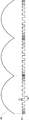
図2は、スイッチング素子10のスイッチング動作を示す電圧波形である。同図において、20はダイオードブリッジ5により全波整流された後の直流電圧波形であり、21はPWM制御IC11からスイッチング素子10のゲートに入力されるパルス波形である。トランス7の一次巻線7aに接続されたスイッチング素子10は、ゲートにPWM制御IC11からパルス波形21が入力されることで、スイッチング動作を行う。すなわちスイッチング素子10のゲートにHレベルが入力されるとターンオンし、Lレベルが入力されるとターンオフする。スイッチング素子10がオン・オフ動作すると、一次巻線7aに直流電圧が断続的に印加され、トランス7の二次巻線7aに電圧が誘起され、整流平滑15により整流平滑されることで出力電圧となる。
FIG. 2 is a voltage waveform showing the switching operation of the
このとき、PWM制御IC11は、出力電圧検出回路18から送られるフィードバック信号に基づきPWM制御を行ないながらパルスを出力する。すなわち、出力電圧を安定させるためスイッチング素子10のゲートに入力するパルス波形21の導通幅t1を増減させながら、周期t0毎にパルスを出力する。スイッチング素子10の制御周波数を表す該パルス周期t0は、前述したようにPWM制御IC11の抵抗接続端子11aに接続された抵抗12の抵抗値により、その大きさが変化する。これは、PWM制御IC11を構成する発振回路であるオシレータ(OSCILATOR)の入力端子としての抵抗接続端子11aから流れ出る電流値により、スイッチング素子10の制御周波数が変化するということである。ここで、PWM制御IC11の抵抗接続端子11aには、直流電圧波形20を抵抗14と抵抗12とにより分圧した電圧が印加されている。従って、直流電圧波形20の値が大きくなると、PWM制御IC11の抵抗接続端子11aから流れ出る電流が小さくなり、スイッチング素子10の制御周波数も低くなる。反対に、直流電圧波形20の値が小さくなると、PWM制御IC11の抵抗接続端子11aから流れ出る電流が大きくなり、スイッチング素子10の制御周波数も高くなる。このようにして、スイッチング素子10の制御周波数ひいてはスイッチング周波数は、電圧波形20の変化に伴い、揺らぐように変化する。
At this time, the
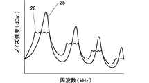
図3は、本実施例におけるスイッチング電源で発生するノイズの測定結果を例示したものであるが、25は抵抗14を設けない場合の出力周波数スペクトラムであり、26は抵抗14を設けた場合の出力周波数スペクトラムである。抵抗14を設けない場合では、PWM制御IC11の制御周波数が一定に固定されているため、スイッチング素子10のスイッチング周波数に対応する周波数帯にノイズが集中して発生し、ノイズ強度のピークが大きく突出する形となっている。一方、抵抗14を設けた場合では、PWM制御IC11の制御周波数に揺らぎがあるため、スイッチング素子10のスイッチング周波数が変化する帯域幅でノイズが分散され、ノイズ強度のピークが大きく突出していないのがわかる。なお、このようなスイッチングノイズは、スイッチング周波数のn倍波に対応する帯域毎に現れるため、ある帯域幅でのノイズ強度のピークが平均化され、低減されることとなる。
FIG. 3 exemplifies the measurement result of the noise generated in the switching power supply in this embodiment. 25 is an output frequency spectrum when the
以上のように本実施例では、スイッチング素子10をオン・オフ動作させることにより交流入力電源2から供給される交流電圧から出力電圧を取り出すスイッチング電源装置1において、前記スイッチング素子10のオン・オフ動作を制御する制御周波数を前記交流電圧の振幅に応じて変化させるスイッチング制御手段としてのPWM制御11を備えるよう構成している。
As described above, in this embodiment, the
また、交流入力電源2から供給される交流電圧をダイオードブリッジ5により全波整流すると共に、抵抗14と抵抗12とで前記整流電圧を分圧し、PWM制御IC11を構成する発振回路であるオシレータの入力端子としての抵抗接続端子11aに印加することにより、抵抗接続端子11aから流れ出る電流の値に揺らぎを生じさせている。
Further, the AC voltage supplied from the AC input power source 2 is full-wave rectified by the diode bridge 5, and the rectified voltage is divided by the
このようにすると、スイッチング素子10のオン・オフ動作を制御する制御周波数が、交流入力電源2から供給される交流電圧の振幅に応じて増減するため、制御周波数に揺らぎが生じる。該制御周波数に揺らぎが生じると、スイッチング周波数が一定とならず、スイッチング周波数のn倍波に対応する帯域毎に集中して発生していたノイズが、スイッチング周波数が揺らいでいる帯域幅で分散されることとなる。従って、ある帯域幅でのノイズ強度のピークが平均化され、低減することができる。また、元々揺らぎを有する交流電力の振幅に応じて、制御周波数を変化させるだけでよいので、簡単な構成でノイズを抑制することができる。
In this way, the control frequency for controlling the on / off operation of the switching
なお、本発明は、上記実施例に限定されるものではなく、本発明の趣旨を逸脱しない範囲で変更可能である。スイッチング電源は、フォワード形,フライバック形,ハーフブリッジ形,フルブリッジ形などの各種方式でもよく、一石式,多石式いずれのものでもよい。 In addition, this invention is not limited to the said Example, It can change in the range which does not deviate from the meaning of this invention. The switching power supply may be of various types such as forward type, flyback type, half bridge type, full bridge type, etc., and may be either a single stone type or a multi stone type.
1 スイッチング電源装置
10 スイッチング素子
11 PWM制御IC(スイッチング制御手段)
1 Switching power supply
10 Switching element
11 PWM control IC (switching control means)
Claims (1)
In a switching power supply device that extracts an output voltage from an alternating voltage by turning on / off the switching element, switching control means for changing a control frequency for controlling the on / off operation of the switching element according to the amplitude of the alternating voltage A switching power supply device comprising:
Priority Applications (1)
| Application Number | Priority Date | Filing Date | Title |
|---|---|---|---|
| JP2004104587A JP4356110B2 (en) | 2004-03-31 | 2004-03-31 | Switching power supply |
Applications Claiming Priority (1)
| Application Number | Priority Date | Filing Date | Title |
|---|---|---|---|
| JP2004104587A JP4356110B2 (en) | 2004-03-31 | 2004-03-31 | Switching power supply |
Publications (2)
| Publication Number | Publication Date |
|---|---|
| JP2005295637A true JP2005295637A (en) | 2005-10-20 |
| JP4356110B2 JP4356110B2 (en) | 2009-11-04 |
Family
ID=35327975
Family Applications (1)
| Application Number | Title | Priority Date | Filing Date |
|---|---|---|---|
| JP2004104587A Expired - Fee Related JP4356110B2 (en) | 2004-03-31 | 2004-03-31 | Switching power supply |
Country Status (1)
| Country | Link |
|---|---|
| JP (1) | JP4356110B2 (en) |
Cited By (5)
| Publication number | Priority date | Publication date | Assignee | Title |
|---|---|---|---|---|
| JP2007124886A (en) * | 2005-09-29 | 2007-05-17 | Clarion Co Ltd | Switching power supply device |
| JP2008017667A (en) * | 2006-07-07 | 2008-01-24 | Tinyplug Technology (Shenzhen) Ltd | Plugged power supply unit |
| US7778050B2 (en) | 2007-12-07 | 2010-08-17 | Panasonic Corporation | Energy transfer device and energy transfer control semiconductor device |
| US8289738B2 (en) | 2009-03-27 | 2012-10-16 | Fuji Electric Co., Ltd. | Switching power supply |
| EP4472052A1 (en) * | 2023-05-30 | 2024-12-04 | Infineon Technologies Austria AG | Method for operating a power converter, control circuit, and power converter |
-
2004
- 2004-03-31 JP JP2004104587A patent/JP4356110B2/en not_active Expired - Fee Related
Cited By (5)
| Publication number | Priority date | Publication date | Assignee | Title |
|---|---|---|---|---|
| JP2007124886A (en) * | 2005-09-29 | 2007-05-17 | Clarion Co Ltd | Switching power supply device |
| JP2008017667A (en) * | 2006-07-07 | 2008-01-24 | Tinyplug Technology (Shenzhen) Ltd | Plugged power supply unit |
| US7778050B2 (en) | 2007-12-07 | 2010-08-17 | Panasonic Corporation | Energy transfer device and energy transfer control semiconductor device |
| US8289738B2 (en) | 2009-03-27 | 2012-10-16 | Fuji Electric Co., Ltd. | Switching power supply |
| EP4472052A1 (en) * | 2023-05-30 | 2024-12-04 | Infineon Technologies Austria AG | Method for operating a power converter, control circuit, and power converter |
Also Published As
| Publication number | Publication date |
|---|---|
| JP4356110B2 (en) | 2009-11-04 |
Similar Documents
| Publication | Publication Date | Title |
|---|---|---|
| US6366476B1 (en) | Switching power supply apparatus with active clamp circuit | |
| US6344986B1 (en) | Topology and control method for power factor correction | |
| KR100342590B1 (en) | Pulsewidth modulation signal generator and switching mode power supply using pulsewidth modulation signal generator | |
| US7388762B2 (en) | Switching power supply circuit | |
| WO2013080403A1 (en) | Switching power supply apparatus and semiconductor device | |
| JP2017017767A (en) | High efficiency power factor improvement circuit and switching power supply device | |
| JP2016119761A (en) | Switching power supply circuit | |
| US20110085356A1 (en) | Switching element driving control circuit and switching power supply device | |
| CN112953199A (en) | Switching power supply controller and control method thereof | |
| CN110401347B (en) | DC power supply unit | |
| KR20150137872A (en) | Apparatus for supplying power and power transformer circuit thereof | |
| JP2004201385A (en) | Dc-dc converter circuit | |
| JP6356545B2 (en) | Switching power supply | |
| JP4356110B2 (en) | Switching power supply | |
| JP2005245142A (en) | Semiconductor device for controlling switching power supply | |
| JP6379877B2 (en) | High efficiency power factor correction circuit and switching power supply | |
| JP5136317B2 (en) | Power supply | |
| JP2006050760A (en) | Switching power supply circuit and control method therefor | |
| JP4308183B2 (en) | Semiconductor device for switching power supply control and switching power supply device | |
| US6580624B2 (en) | Switching power circuit with a filter for controlling noise of a switching frequency and method of same | |
| JPH07170731A (en) | Stabilized power supply | |
| JP4899709B2 (en) | Switching power supply device and electronic device | |
| JP5381027B2 (en) | DC-DC converter | |
| JP2004328837A (en) | Switching power supply circuit and switching regulator comprising the same | |
| JP2005318224A (en) | Receiver |
Legal Events
| Date | Code | Title | Description |
|---|---|---|---|
| A621 | Written request for application examination |
Free format text: JAPANESE INTERMEDIATE CODE: A621 Effective date: 20051207 |
|
| A131 | Notification of reasons for refusal |
Free format text: JAPANESE INTERMEDIATE CODE: A131 Effective date: 20090205 |
|
| A521 | Request for written amendment filed |
Free format text: JAPANESE INTERMEDIATE CODE: A523 Effective date: 20090327 |
|
| A131 | Notification of reasons for refusal |
Free format text: JAPANESE INTERMEDIATE CODE: A131 Effective date: 20090427 |
|
| A521 | Request for written amendment filed |
Free format text: JAPANESE INTERMEDIATE CODE: A523 Effective date: 20090619 |
|
| TRDD | Decision of grant or rejection written | ||
| A01 | Written decision to grant a patent or to grant a registration (utility model) |
Free format text: JAPANESE INTERMEDIATE CODE: A01 Effective date: 20090713 |
|
| A01 | Written decision to grant a patent or to grant a registration (utility model) |
Free format text: JAPANESE INTERMEDIATE CODE: A01 |
|
| A61 | First payment of annual fees (during grant procedure) |
Free format text: JAPANESE INTERMEDIATE CODE: A61 Effective date: 20090726 |
|
| FPAY | Renewal fee payment (event date is renewal date of database) |
Free format text: PAYMENT UNTIL: 20120814 Year of fee payment: 3 |
|
| R150 | Certificate of patent or registration of utility model |
Ref document number: 4356110 Country of ref document: JP Free format text: JAPANESE INTERMEDIATE CODE: R150 Free format text: JAPANESE INTERMEDIATE CODE: R150 |
|
| S531 | Written request for registration of change of domicile |
Free format text: JAPANESE INTERMEDIATE CODE: R313531 |
|
| FPAY | Renewal fee payment (event date is renewal date of database) |
Free format text: PAYMENT UNTIL: 20120814 Year of fee payment: 3 |
|
| R350 | Written notification of registration of transfer |
Free format text: JAPANESE INTERMEDIATE CODE: R350 |
|
| FPAY | Renewal fee payment (event date is renewal date of database) |
Free format text: PAYMENT UNTIL: 20130814 Year of fee payment: 4 |
|
| LAPS | Cancellation because of no payment of annual fees |