JP2005295631A - Power supply device and power supply control device - Google Patents
Power supply device and power supply control device Download PDFInfo
- Publication number
- JP2005295631A JP2005295631A JP2004104472A JP2004104472A JP2005295631A JP 2005295631 A JP2005295631 A JP 2005295631A JP 2004104472 A JP2004104472 A JP 2004104472A JP 2004104472 A JP2004104472 A JP 2004104472A JP 2005295631 A JP2005295631 A JP 2005295631A
- Authority
- JP
- Japan
- Prior art keywords
- output
- detection pulse
- pulse
- power supply
- load
- Prior art date
- Legal status (The legal status is an assumption and is not a legal conclusion. Google has not performed a legal analysis and makes no representation as to the accuracy of the status listed.)
- Granted
Links
Images
Landscapes
- Dc-Dc Converters (AREA)
Abstract
【課題】一端に入力電圧が印加されたコイルの他端を、負荷と接地とで交互に接続することにより、入力電圧を昇圧して、負荷への電源供給を安定化できる電源装置及び電源制御装置を提供する。
【解決手段】一端に入力電圧Vinが印加されたコイルLOの他端を、負荷12と接地とで交互に接続することにより、入力電圧を昇圧して、負荷に供給する電源装置において、負荷に印加される電圧に応じたパルス幅の第1の検出パルスを生成する第1の検出パルス生成手段R1,21,22,26,27.123と、コイルに流れる電流に応じたパルス幅の第2の検出パルスを生成する第2の検出パルス生成手段R11;21,22,121,122,124;221,222,223とで生成された第1の検出パルスと第2の検出パルスとを合成した出力パルスに応じてコイルの他端の負荷と接地とに接続する期間を制御する制御手段28,M11,M12とを有する。
【選択図】図1A power supply apparatus and a power supply control capable of stabilizing the power supply to a load by boosting the input voltage by alternately connecting the other end of a coil having an input voltage applied to one end between a load and a ground. Providing the device.
In a power supply device that boosts an input voltage by alternately connecting the other end of a coil LO, to which an input voltage Vin is applied at one end, between a load and a ground, and supplying the load to the load, First detection pulse generation means R1, 21, 22, 26, 27.123 for generating a first detection pulse having a pulse width corresponding to the applied voltage, and a second detection having a pulse width corresponding to the current flowing through the coil A second detection pulse generating means for generating a pulse R11; 21, 22, 121, 122, 124; 221, 222, 223; a load at the other end of the coil according to an output pulse obtained by combining the first detection pulse and the second detection pulse; Control means 28, M11, M12 for controlling the period of connection to the ground.
[Selection] Figure 1
Description
本発明は電源装置及び電源制御装置に係り、特に、一端に入力電圧が印加されたコイルの他端を、負荷と接地とで交互に接続することにより、入力電圧を昇圧して、負荷に供給する電源装置及び電源制御装置に関する。 The present invention relates to a power supply device and a power supply control device, and in particular, by alternately connecting the other end of a coil having an input voltage applied to one end between a load and a ground, the input voltage is boosted and supplied to the load. The present invention relates to a power supply device and a power supply control device.
近年、携帯電話を始めとした携帯機器が広く普及している。携帯機器は、電池で駆動されるため、その表示装置として液晶ディスプレイパネルが搭載されている。 In recent years, mobile devices such as mobile phones have become widespread. Since the portable device is driven by a battery, a liquid crystal display panel is mounted as the display device.
液晶ディスプレイパネルは、自発光型ではないので、光源が必要となる。液晶ディスプレイパネルの光源としては、外光の他、陰極線管やLEDなどがある。 Since the liquid crystal display panel is not a self-luminous type, a light source is required. As a light source of the liquid crystal display panel, there are a cathode ray tube, an LED and the like in addition to external light.
携帯機器に搭載される液晶ディスプレイの光源としては、高輝度、高効率であり、かつ、小型化が可能である白色LEDを用いた光源が注目されている。液晶ディスプレイの光源として白色LEDを搭載する場合には、画面のちらつきを防いだり、輝度を均一化したりするために複数のLEDを直列接続して使用している。 As a light source of a liquid crystal display mounted on a portable device, a light source using a white LED that has high luminance, high efficiency, and can be miniaturized has attracted attention. When a white LED is mounted as a light source of a liquid crystal display, a plurality of LEDs are connected in series in order to prevent flickering of the screen and to make the luminance uniform.
このとき、携帯機器の電池は、小型化、小電力化のため低電圧化されているため、直列接続された複数のLEDを駆動するには電圧が低すぎる。このため、電池電圧を昇圧してLEDを駆動するための電源電圧を得る昇圧型の電源回路が搭載されている(特許文献1参照)。 At this time, since the battery of the portable device has a low voltage for miniaturization and low power consumption, the voltage is too low to drive a plurality of LEDs connected in series. For this reason, a booster type power supply circuit that boosts the battery voltage and obtains a power supply voltage for driving the LED is mounted (see Patent Document 1).
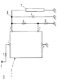
図7は従来の一例のブロック構成図を示す。 FIG. 7 shows a block diagram of an example of the prior art.
従来の電源装置1は、コイルL0、電流制御IC(integrated circuit)11、平滑用キャパシタC1、負荷電流検出用抵抗R1から構成され、入力電圧Vinを昇圧した出力電圧Voutを負荷12に印加する。
The conventional
コイルL0の一端には、入力電圧Vinが印加されている。コイルL0の他端は、電流制御IC11の端子T1に接続されている。負荷12は、例えば、発光ダイオードD1〜Dnを直列接続した構成されており、アノード側が電流制御IC11の端子T2に接続され、カソード側が負荷電流検出用抵抗R1を介して接地に接続された構成とされている。負荷電流検出用抵抗R1には、出力電圧Voutに応じた電圧Vsが発生する。負荷電流検出用抵抗R1に発生した電圧Vsは、電流検出IC11の端子T3に印加される。
An input voltage Vin is applied to one end of the coil L0. The other end of the coil L0 is connected to the terminal T1 of the current control IC11. The
電流制御IC11は、発振回路21、波形整形回路22、加算回路23、コンパレータ24、25、誤差アンプ26、基準電圧源27、ドライバ28、抵抗R11、MOSトランジスタM11、M12が内蔵された構成とされている。発振回路21は、所定の周波数で発振を行っている。発振回路21の発振出力は、波形整形回路22に供給される。波形整形回路22は、発振回路21から供給された発振出力で発振された発振出力をランプ波形状に波形整形する。波形整形回路22で波形整形されたランプ波形状の信号は、加算回路23に供給される。加算回路23には、波形整形回路22からのランプ波形状の信号の他にコンパレータ24の出力が供給されている。
The
コンパレータ24は、抵抗R11の両端の電圧が所定電圧より大きいときに出力をハイレベルとし、抵抗R11の両端の電圧が所定電圧より小さいときに出力をローレベルとする。抵抗R11は、一端がMOSトランジスタM11に接続され、他端が接地端子T4に接続されており、MOSトランジスタM11に流れる電流に応じた電圧がその両端に発生する。MOSトランジスタM11は、ソース−ドレインが端子T1と抵抗R11の一端との間に接続されている。また、MOSトランジスタM11のゲートには、ドライバ28から駆動パルスが供給される。MOSトランジスタM11は、ドライバ28からの駆動パルスがハイレベルのときにオンし、端子T1から電流を引き込み、ドライバ28からの駆動パルスがローレベルのときにオフし、端子T1からの電流の引き込みを停止する。
The
抵抗R11の両端の電圧を検出することにより、端子T1から引き込まれる電流、すなわち、コイルL0に流れる電流を検出することができる。 By detecting the voltage across the resistor R11, the current drawn from the terminal T1, that is, the current flowing through the coil L0 can be detected.
加算回路23は、波形整形回路22のランプ波形状の信号とコンパレータ24の出力とを加算する。加算回路23の出力は、コンパレータ25の非反転入力端子に供給される。
The
コンパレータ25の反転入力端子には、誤差アンプ26の出力が供給されている。誤差アンプ26は、反転入力端子が端子T3に接続されており、非反転入力端子に基準電圧源27から基準電圧が印加されており、反転増幅回路を構成している。誤差アンプ26は、 端子T3に供給される負荷電流に応じた電圧Vsと基準電圧との差電圧に応じた信号を出力する。
The output of the
コンパレータ25は、加算回路23の出力が誤差アンプ26の出力より大きいときに出力をハイレベルとし、加算回路23の出力が誤差アンプ26の出力小さいときに出力をローレベルとする。コンパレータ25の出力パルスは、ドライバ28に供給される。ドライバ28は、コンパレータ25の出力パルスがハイレベルのときにはMOSトランジスタM11、M12のゲート電圧をローレベルとし、コンパレータ25の出力がローレベルのときにはMOSトランジスタM11、M12のゲート電圧をハイレベルとする。
The comparator 25 sets the output to a high level when the output of the
MOSトランジスタM11は、nチャネルMOS電界効果トランジスタから構成されており、ドライバ28の出力がハイレベルのときにはオンし、ドライバ28の出力がローレベルのときにはオフする。MOSトランジスタM12は、pチャネルMOS電界効果トランジスタから構成されており、ドライバ28の出力がハイレベルのときにはオフし、ドライバ28の出力がローレベルのときにはオンする。これによって、MOSトランジスタM11とMOSトランジスタM12とは、コンパレータ25の出力パルスに応じて互いに交互にオン/オフする。
The MOS transistor M11 is composed of an n-channel MOS field effect transistor, and is turned on when the output of the
MOSトランジスタM11がオンし、MOSトランジスタM12がオフした状態では、端子T1が接地され、コイルL0に電流が流れる。次に、MOSトランジスタM11がオフし、MOSトランジスタM12がオンすると、コイルL0に逆起電力が発生し、この逆起電力により端子T1の電圧が昇圧される。端子T1に生じた昇圧電圧は、端子T2から負荷12に供給される。
When the MOS transistor M11 is turned on and the MOS transistor M12 is turned off, the terminal T1 is grounded, and a current flows through the coil L0. Next, when the MOS transistor M11 is turned off and the MOS transistor M12 is turned on, a back electromotive force is generated in the coil L0, and the voltage at the terminal T1 is boosted by this back electromotive force. The boosted voltage generated at the terminal T1 is supplied to the
このとき、負荷12に流れる負荷電流が増加すると、負荷電流検出用抵抗R1に発生する電圧Vsが上昇する。電圧Vsが上昇すると、誤差アンプ26の出力が低下する。誤差アンプ26の出力が低下すると、コンパレータ25の出力パルスがハイレベルとなる期間が長くなる。コンパレータ25の出力パルスのハイレベルの期間が長くなると、ドライバ28の出力駆動パルスのローレベルの期間が長くなり、MOSトランジスタM11のオフする期間が長くなる。これによって、出力電圧Voutが低減し、負荷12に流れる負荷電流が減少する。
At this time, when the load current flowing through the
また、負荷12に流れる負荷電流が減少すると、負荷電流検出用抵抗R1に発生する電圧Vsが低下する。電圧Vsが低下すると、誤差アンプ26の出力が上昇する。誤差アンプ26の出力が上昇すると、コンパレータ25の出力パルスがハイレベルとなる期間が短くなる。コンパレータ25の出力パルスのハイレベルの期間が短くなると、ドライバ28の出力駆動パルスのローレベルの期間が短くなり、MOSトランジスタM11のオフする期間が短くなる。これによって、出力電圧Voutが増加し、負荷12に流れる負荷電流が増加する。
Further, when the load current flowing through the
上記のようにPWM制御が行われ、負荷12に流れる負荷電流が一定となるように出力電圧Voutが制御されていた。
The PWM control is performed as described above, and the output voltage Vout is controlled so that the load current flowing through the
また、このとき、電流制御IC11は、端子T1から引き込まれる電流を監視することにより、コイルL0に流れる電流が過電流状態とならないように制御していた。端子T1から引き込まれる電流が過電流状態になると、MOSトランジスタM11がオンしたとき、抵抗R11の両端に発生する電圧が増加し、コンパレータ24の出力パルスがハイレベルとなる。コンパレータ24の出力パルスがハイレベルになると、波形整形回路22の出力信号であるランプ波形状の信号にコンパレータ24の出力パルスが加算され、波形整形回路22の出力信号がコンパレータ24の出力パルスのハイレベル分だけハイレベル方向にシフトする。
At this time, the
波形整形回路22の出力信号がコンパレータ24の出力パルスのハイレベル分だけハイレベル方向にシフトすると、コンパレータ25の出力パルスが誤差アンプ26の出力によらず、ハイレベルに保持される。コンパレータ25の出力パルスがハイレベルに保持されると、MOSトランジスタM11が負荷12に流れる負荷電流によらずオフされ、端子T1から電流は引き込まれず、過電流状態を解消できる。
When the output signal of the
また、端子T1から引き込まれる電流が過電流状態でない場合には、MOSトランジスタM11がオンしたとき、抵抗R11の両端に発生する電圧は規定値より小さいので、コンパレータ24の出力パルスはローレベルとなる。コンパレータ24の出力パルスがローレベルの場合には、波形整形回路22の出力信号であるランプ波形状の信号レベルは、誤差アンプ26の出力と比較可能なレベルに維持される。これによって、コンパレータ25の出力パルスは、誤差アンプ26の出力に応じてハイレベルの期間が制御される。これによって、MOSトランジスタM11、M12は、通常のように、PWM制御が行われ、負荷12に流れる負荷電流が一定となるように出力電圧Voutが制御される。
When the current drawn from the terminal T1 is not in an overcurrent state, when the MOS transistor M11 is turned on, the voltage generated at both ends of the resistor R11 is smaller than the specified value, so that the output pulse of the
しかるに、従来の電源装置では、ランプ波形の上下シフトによって、過電流制御を行っていた。 However, in the conventional power supply device, overcurrent control is performed by shifting the ramp waveform up and down.
このとき、リプル電流をΔI、リプル出力をΔV、動作周波数をf、出力容量をCoutとすると、出力リプルΔVは、一般に、
ΔV=ΔI/8fCout ・・・(1)
で表される。ここで、リプル電流ΔI及び出力容量Coutを一定とすると、出力リプルΔVは、動作周波数fで決定される。
At this time, assuming that the ripple current is ΔI, the ripple output is ΔV, the operating frequency is f, and the output capacitance is Cout, the output ripple ΔV is generally
ΔV = ΔI / 8fCout (1)
It is represented by Here, assuming that the ripple current ΔI and the output capacitance Cout are constant, the output ripple ΔV is determined by the operating frequency f.
このとき、従来の電源装置では、コンパレータ24の出力によりランプ波形が上下シフトするため、いわゆる、PFM制御のような動作となり、動作周波数が低い方向に変動し、出力リプルΔVが増加するなどの問題点があった。
At this time, in the conventional power supply device, the ramp waveform is shifted up and down by the output of the
本発明は上記の点に鑑みてなされたもので、負荷への電源供給を安定化できる電源装置及び電源制御装置を提供することを目的とする。 The present invention has been made in view of the above points, and an object of the present invention is to provide a power supply device and a power supply control device that can stabilize power supply to a load.
本発明は、一端に入力電圧(Vin)が印加されたコイル(L0)の他端を、負荷(12)と接地とで交互に接続することにより、入力電圧(Vin)を昇圧して、負荷(12)に供給する電源装置において、負荷(12)に印加される電圧に応じたパルス幅の第1の検出パルスを生成する第1の検出パルス生成手段(R1、21、22、26、27、123)と、コイル(L0)に流れる電流に応じたパルス幅の第2の検出パルスを生成する第2の検出パルス生成手段(R11;21、22、121、122、124;221、222、223)と、第1の検出パルス生成手段(R1、21、22、26、27、123)で生成された第1の検出パルスと第2の検出パルス生成手段(R11;21、22、121、122、124;221、222、223)で生成された第2の検出パルスとを合成した出力パルスを生成する出力パルス生成手段(125)と、出力パルス生成手段(125)で生成された出力パルスに応じてコイル(L0)の他端の、負荷(12)と接地とに接続する期間を制御する制御手段(28、M11、M12)とを有することを特徴とする。 The present invention boosts the input voltage (Vin) by alternately connecting the other end of the coil (L0), to which the input voltage (Vin) is applied at one end, with the load (12) and the ground. In the power supply device supplied to (12), first detection pulse generating means (R1, 22, 22, 26, 27 for generating a first detection pulse having a pulse width corresponding to the voltage applied to the load (12). , 123) and second detection pulse generation means (R11; 21, 22, 121, 122, 124; 221, 222, which generates a second detection pulse having a pulse width corresponding to the current flowing through the coil (L0). 223), the first detection pulse generated by the first detection pulse generation means (R1, 22, 22, 26, 27, 123) and the second detection pulse generation means (R11; 21, 22, 121, 122, 124; 221, 222, Output pulse generating means (125) for generating an output pulse obtained by synthesizing the second detection pulse generated in (23), and the coil (L0) according to the output pulse generated by the output pulse generating means (125). It has a control means (28, M11, M12) for controlling the period of connection to the load (12) and the ground at the other end.
また、第1の検出パルス生成手段(R1、21、22、26、27、123)及び第2の検出パルス生成手段(R11;21、22、121、122、124;221、222、223)は、共通する発振手段(21、22)を有し、第1の検出パルス生成手段(R1、21、22、26、27、123)は、発振手段(21、22)で生成される発振出力に同期して第1の検出パルスを生成し、第2の検出パルス生成手段(R11;21、22、121、122、124;221、222、223)は、発振手段(21、22)で生成される発振出力に同期して第2の検出パルスを生成することを特徴とする。 The first detection pulse generation means (R1, 22, 22, 26, 27, 123) and the second detection pulse generation means (R11; 21, 22, 121, 122, 124; 221, 222, 223) The first detection pulse generation means (R1, 22, 22, 26, 27, 123) has an oscillation output generated by the oscillation means (21, 22). The first detection pulse is generated synchronously, and the second detection pulse generation means (R11; 21, 22, 121, 122, 124; 221, 222, 223) is generated by the oscillation means (21, 22). The second detection pulse is generated in synchronization with the oscillation output.
さらに、第2の検出パルス生成手段(R11;21、22、121、122、124;221、222、223)で生成された第2の検出パルスの状態が所定期間連続したときに、該状態を出力として反映させるデバウンス回路(223)を有することを特徴とする。 Further, when the state of the second detection pulse generated by the second detection pulse generation means (R11; 21, 22, 121, 122, 124; 221, 222, 223) continues for a predetermined period, the state is changed. It has a debounce circuit (223) reflected as an output.
なお、上記参照符号はあくまでも参考であり、これによって、特許請求の範囲が限定されるものではない。 In addition, the said reference code is a reference to the last, This does not limit a claim.
本発明によれば、第1の検出パルス生成手段で生成された第1の検出パルスと第2の検出パルス生成手段で生成された第2の検出パルスとを合成した出力パルスを生成し、生成された出力パルスに応じてコイルの他端の、負荷又は接地に接続する期間を制御する構成とすることにより、動作を安定化させることができ、よって、負荷への電源供給を安定化させることができるなどの特長を有する。 According to the present invention, an output pulse is generated by combining the first detection pulse generated by the first detection pulse generation unit and the second detection pulse generated by the second detection pulse generation unit. By controlling the period during which the other end of the coil is connected to the load or ground according to the output pulse, the operation can be stabilized, and thus the power supply to the load can be stabilized. It has features such as
また、本発明によれば、発振手段(21、22)で生成される発振出力に同期して第1の検出パルス及び第2の検出パルスを生成することにより、一定の動作周波数で動作させることができるので、さらに、動作を安定化させることができるなどの特長を有する。 Further, according to the present invention, the first detection pulse and the second detection pulse are generated in synchronization with the oscillation output generated by the oscillation means (21, 22), thereby operating at a constant operating frequency. Therefore, the operation can be further stabilized.
〔第1実施例〕
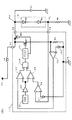
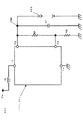
図1は、本発明の第1実施例のブロック構成図を示す。同図中、図7と同一構成部分には同一符号を付し、その説明は省略する。
[First embodiment]
FIG. 1 shows a block diagram of a first embodiment of the present invention. In the figure, the same components as those in FIG.
本実施例の電源装置101は、電源制御IC111の構成が従来の電源装置101とは相違する。電源制御IC101は、発振回路21、波形整形回路22、誤差アンプ26、121、基準電圧源27、122、コンパレータ124、123、論理和回路125、MOSトランジスタM11、M12、抵抗R11から構成される。
The
誤差アンプ26は、反転増幅回路を構成しており、反転端子にはフィードバック端子T3が接続され、非反転端子には基準電圧源27から基準電圧が印加されている。誤差アンプ26は、フィードバック端子T3の電圧と基準電圧との差電圧に応じた信号を出力する。
The
誤差アンプ26の出力は、コンパレータ123の反転入力端子に供給される。コンパレータ123の非反転入力端子には、波形整形回路22から発振回路21の発振出力により生成されたランプ波形状の信号が供給される。コンパレータ123は、誤差アンプ26の出力が波形整形回路22のランプ波形状の出力より小さいときにハイレベルとなり、誤差アンプ26の出力が波形整形回路22のランプ波形状の出力より大きいときにローレベルとなる第1のパルスを出力する。コンパレータ123の出力パルスは、論理和回路125に供給される。
The output of the
誤差アンプ121は、反転増幅回路を構成しており、反転端子にはMOSトランジスタM11と抵抗R11との接続点が接続され、非反転端子には基準電圧源122から基準電圧が印加されている。誤差アンプ121は、MOSトランジスタM11と抵抗R11との接続点の電圧と基準電圧との差電圧に応じた信号を出力する。
The
誤差アンプ121の出力は、コンパレータ124の反転入力端子に供給される。コンパレータ124の非反転入力端子には、波形整形回路22から発振回路21の発振出力により生成されたランプ波形状の信号が供給される。コンパレータ124は、誤差アンプ121の出力が波形整形回路22のランプ波形状の出力より小さいときにハイレベルとなり、誤差アンプ121の出力が波形整形回路22のランプ波形状の出力より大きいときにローレベルとなるパルスを出力する。コンパレータ124の出力パルスは、論理和回路125に供給される。
The output of the
論理和回路125は、コンパレータ123の出力パルスとコンパレータ124の出力パルスとの論理和を出力する。論理和回路125の出力パルスは、ドライバ28に供給される。ドライバ28は、論理和回路125からの出力パルスによりMOSトランジスタM11、M12をスイッチングする。
The OR
次に、電流制御IC111の動作を説明する。 Next, the operation of the current control IC 111 will be described.
フィードバック端子T3の電圧が上昇すると、誤差アンプ26の出力が低下する。誤差アンプ26の出力が低下すると、コンパレータ123の出力パルスのハイレベルの期間が長なり、ローレベルの期間が短くなる。コンパレータ123の出力パルスのハイレベルの期間が長くなり、ローレベルの期間が短くなると、MOSトランジスタM11のオンする期間が短くなり、MOSトランジスタM12のオフする期間が長くなる。これによって、コイルL0に蓄積される電磁エネルギーが小さくなるので、出力電圧Voutが低減する。
When the voltage at the feedback terminal T3 increases, the output of the
また、フィードバック端子T3の電圧が下降すると、誤差アンプ26の出力が上昇する。誤差アンプ26の出力が上昇すると、コンパレータ123の出力パルスのハイレベルの期間が短くなり、ローレベルの期間が長くなる。コンパレータ123の出力パルスのハイレベルの期間が短くなり、ローレベルの期間が長くなると、MOSトランジスタM11のオンする期間が長くなり、MOSトランジスタM12のオフする期間が短くなる。これによって、コイルL0に蓄積される電磁エネルギーが大きくなるので、出力電圧Voutが上昇する。
Further, when the voltage at the feedback terminal T3 decreases, the output of the
また、端子T1から引き込まれる電流が増加すると、MOSトランジスタM11と抵抗R11との接続点の電圧が上昇する。MOSトランジスタM11と抵抗R11との接続点の電圧が上昇すると、誤差アンプ121の出力が低下する。誤差アンプ121の出力が低下すると、コンパレータ124の出力パルスのハイレベルの期間が長なり、ローレベルの期間が短くなる。コンパレータ124の出力パルスのハイレベルの期間が長くなり、ローレベルの期間が短くなると、MOSトランジスタM11のオンする期間が短くなり、MOSトランジスタM12のオフする期間が長くなる。これによって、コイルL0が接地に接続される時間が短くなるため、コイルL0に流れる電流が抑制される。
When the current drawn from the terminal T1 increases, the voltage at the connection point between the MOS transistor M11 and the resistor R11 increases. When the voltage at the connection point between the MOS transistor M11 and the resistor R11 increases, the output of the
端子T1から引き込まれる電流が減少すると、MOSトランジスタM11と抵抗R11との接続点の電圧が下降する。MOSトランジスタM11と抵抗R11との接続点の電圧が下降すると、誤差アンプ121の出力が上昇する。誤差アンプ121の出力が上昇すると、コンパレータ124の出力パルスのハイレベルの期間が短くなり、ローレベルの期間が長くなる。コンパレータ124の出力パルスのハイレベルの期間が短くなり、ローレベルの期間が長くなると、MOSトランジスタM11のオンする期間が長くなり、MOSトランジスタM12のオフする期間が短くなる。これによって、コイルL0が接地に接続される時間が長くなるため、コイルL0に流れる電流が増加する。
When the current drawn from the terminal T1 decreases, the voltage at the connection point between the MOS transistor M11 and the resistor R11 decreases. When the voltage at the connection point between the MOS transistor M11 and the resistor R11 decreases, the output of the
論理和回路125の出力は、コンパレータ123の出力パルスとコンパレータ124の出力パルスのうちハイレベルの長い方、すなわち、トランジスタM11をオフする期間が長い方の出力パルスにより制御が行われる。
The output of the
本実施例によれば、電圧制御を行う第1のパルスによるPWM制御と電流制御を行う第2のパルスによるPWM制御の両方のPWM制御を発振回路21の発振出力により生成される波形整形回路22のランプ波形状の信号に同期して行うことにより、式(1)の動作周波数を一定にできるため、動作を安定化させることができる。
According to the present embodiment, the
〔第2実施例〕
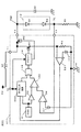
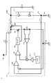
図2は、本発明の第2実施例のブロック構成図を示す。同図中、図1と同一構成部分には同一符号を付し、その説明は省略する。
[Second Embodiment]
FIG. 2 shows a block diagram of the second embodiment of the present invention. In the figure, the same components as in FIG.
本実施例の電源装置201は、誤差アンプ121、基準電圧源122に代えてコンパレータ221、基準電圧源222を設け、コンパレータ124に代えて第2の検出パルスの短期間の変化を吸収し、デバウンス回路223を設けた構成とされている。
The
コンパレータ221は、非反転入力端子に基準電圧源222から基準電圧が印加され、反転入力端子にMOSトランジスタM11と抵抗R11との接続点が接続されており、MOSトランジスタM11と抵抗R11との接続点の電圧が基準電圧より大きければ出力をローレベルとし、MOSトランジスタM11と抵抗R11との接続点の電圧が基準電圧より小さければ出力をハイレベルとする。コンパレータ221の出力パルスはデバウンス回路223に供給される。
In the
デバウンス回路223は、コンパレータ221の出力パルスの状態が所定期間連続したときに、その状態を出力として反映させる。デバウンス回路223の出力は、論理和回路125に供給される。
When the state of the output pulse of the
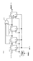
図3は、デバウンス回路223のブロック構成図を示す。
FIG. 3 is a block diagram of the
デバウンス回路223は、分周回路231、Dフリップフロップ232−1〜232−n、233、排他的論和(exclusive or;ex-or)回路234から構成される。
The
分周回路231は、発振回路21の発振出力を分周する。分周回路231の分周比により応答性が決定される。
The
分周回路231の出力は、Dフリップフロップ232−1〜232−n、233に動作クロックとして供給される。Dフリップフロップ232−1は、データ端子Dにコンパレータ221の出力パルスが供給されている。Dフリップフロップ232−1は、分周回路231からのクロックの立ち上がり時のデータ端子Dの状態を読み込み、出力端子Qから出力する。Dフリップフロップ232−2は、データ端子DにDフリップフロップ232−1の出力端子Qが接続されている。Dフリップフロップ232−2は、分周回路231からのクロックの立ち上がり時のデータ端子Dの状態を読み込み、出力端子Qから出力する。
The output of the
Dフリップフロップ232−3は、データ端子DにDフリップフロップ232−2の出力端子Qが接続されている。Dフリップフロップ232−3は、分周回路231からのクロックの立ち上がり時のデータ端子Dの状態を読み込み、出力端子Qから出力する。なお、Dフリップフロップ232−4〜232−nは、同様にして順次に接続されている。Dフリップフロップ232−1〜232−nによりコンパレータ221の出力パルスを遅延している。
In the D flip-flop 232-3, the output terminal Q of the D flip-flop 232-2 is connected to the data terminal D. The D flip-flop 232-3 reads the state of the data terminal D at the rising edge of the clock from the
Dフリップフロップ232−nの出力端子Qは、Dフリップフロップ233のデータ端子Dに接続されている。Dフリップフロップ233は、分周回路231からのクロックの立下り時のデータ端子Dの状態を読み込み、出力端子Qから出力する。Dフリップフロップ233の出力端子Qが論理和回路125に供給される。
The output terminal Q of the D flip-flop 232-n is connected to the data terminal D of the D flip-
排他的論理和回路234には、Dフリップフロップ233の出力端子Qの出力が供給されている。排他的論理和回路234は、Dフリップフロップ232−1〜232−nの出力の排他的論理和を出力する。排他的論理和回路234の出力は、Dフリップフロップ233のイネーブル端子ENに供給される。Dフリップフロップ233は、排他的論理和回路234の出力がハイレベル、すなわち、Dフリップフロップ232−1〜232−nの出力のすべてがハイレベル又はローレベルのときに、イネーブルされ、出力端子Qから出力を行う。
The output from the output terminal Q of the D flip-
このため、コンパレータ221の出力パルスがnクロック連続してハイレベル又はローレベルとなったときにだけ、Dフリップフロップ233の出力が反転する。すなわち、コンパレータ221の出力パルスの状態が所定期間連続したときに、その状態を出力として反映させることができる。
For this reason, the output of the D flip-
また、Dフリップフロップ232−1〜232−n、233のリセット端子Rには、端子T11が接続されている。端子T11には、外部からコントロール信号が供給される。コントロール信号により、Dフリップフロップ232−1〜232−n、233をリセットすることにより、コントロール信号によって制御を行うことが可能となる。 The terminal T11 is connected to the reset terminal R of the D flip-flops 232-1 to 232-n, 233. A control signal is supplied to the terminal T11 from the outside. By resetting the D flip-flops 232-1 to 232-n and 233 by the control signal, it becomes possible to perform control by the control signal.
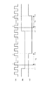
図4は、デバウンス回路223の動作波形図を示す。図4(A)は分周回路231の出力クロック、図4(B)はコンパレータ221の出力パルス、図4(C)はDフリップフロップ233の出力を示す。
FIG. 4 shows an operation waveform diagram of the
図4(B)に示すように時刻t1でコンパレータ221の出力がハイレベルからローレベルに立ち下がると、図4(A)に示すクロックのコンパレータ221の出力がローレベルになった後の次の立ち上がりとなる時刻t2でコンパレータ221の出力がDフリップフロップ232−1に取り込まれる。
As shown in FIG. 4B, when the output of the
時刻t2からnクロック経過してDフリップフロップ232−1〜232−nの出力がすべてローレベルになると、第nクロックの立下りの時刻t3で図4(C)に示すようにDフリップフロップ233の出力がローレベルに立ち下がる。
When n clocks have elapsed from time t2 and all the outputs of the D flip-flops 232-1 to 232-n are at a low level, the D flip-
同様に、図4(B)に示すように時刻t11でコンパレータ221の出力がローレベルからハイレベルに立ち上がると、図4(A)に示すクロックのコンパレータ221の出力がハイレベルになった後、次の立ち上がりとなる時刻t12でコンパレータ221の出力がDフリップフロップ232−1に取り込まれる。
Similarly, when the output of the
時刻t12からnクロック経過してDフリップフロップ232−1〜232−nの出力がすべてハイレベルになると、第nクロックの立下りの時刻t13で図4(C)に示すようにDフリップフロップ233の出力がハイレベルに立ち上がる。
When n clocks have elapsed from time t12 and the outputs of D flip-flops 232-1 to 232-n all become high level, as shown in FIG. 4C, D flip-
以上により、コンパレータ221の出力の状態がデバウンス時間T0、連続したときに、その状態を出力に反映させることができる。なお、デバウンス時間は、Dフリップフロップの段数nによって調整することが可能である。
As described above, when the output state of the
本実施例によれば、デバウンス回路223を設けることにより、デバウンス回路223に設定された遅延時間により式(1)の動作周波数fが決定され、動作周波数fを低い周波数に設定できるため、リプル電圧ΔVを低減できる。
According to the present embodiment, since the
〔変形例〕
図5は、本発明の第1及び第2実施例の変形例のブロック構成図を示す。同図中、図1、図2と同一構成部分には同一符号を付し、その説明は省略する。
[Modification]
FIG. 5 is a block diagram showing a modification of the first and second embodiments of the present invention. In the figure, the same components as those in FIGS. 1 and 2 are denoted by the same reference numerals, and the description thereof is omitted.
本変形例の電源装置301は、電流制御IC111、211の端子T2と接地との間に抵抗R21と抵抗R22とを直列に接続し、抵抗R21と抵抗R22との接続点を電流制御IC111、211の端子T3に接続することにより、出力電圧Voutを検出するようにしたものである。
In the
図6は、本発明の第1及び第2実施例の他の変形例のブロック構成図を示す。同図中、図5と同一構成部分には同一符号を付し、その説明は省略する。 FIG. 6 is a block diagram showing another modification of the first and second embodiments of the present invention. In the figure, the same components as those in FIG.
本変形例の電源装置401は、負荷12に代えて、蓄電池402を充電する構成としたものである。本変形例によれば、電源制御IC111、211を用いて昇圧型の電源装置を構成することにより、電圧制御と電流制御の両方を安定した動作で行えるため、蓄電池402などの充電に用いることが可能となる。
The
〔その他〕
なお、本実施例では、MOSトランジスタM12を電流制御IC111、211に内蔵したが、MOSトランジスタM12は外付けとしてもよい。また、電圧検出用抵抗R1を電流制御IC111、211に内蔵する構成としてもよい。
[Others]
In this embodiment, the MOS transistor M12 is built in the
また、本実施例では、MOSトランジスタM11とMOSトランジスタ12とを同期してスイッチングさせることにより、いわゆる、同期整流型の電源装置に適用した例について説明したが、MOSトランジスタM12に代えてショットキーバリアダイオードなどのダイオードを接続した、いわゆる、整流型の電源装置に適用することも可能である。
In the present embodiment, an example in which the MOS transistor M11 and the
101、201、301、401 電源装置
12 負荷、L0 コイル、C1 平滑用キャパシタ、R1 電圧検出用抵抗
R11 電流検出用抵抗
M11、M12 MOSトランジスタ
21 発振回路、22 波形整形回路、26、121 誤差アンプ
27、122 基準電圧源
28 ドライバ
111、211 電源制御IC
123、124 コンパレータ、125 論理和回路
101, 201, 301, 401
123, 124 Comparator, 125 OR circuit
Claims (6)
前記負荷に流れる電流に応じたパルス幅の第1の検出パルスを生成する第1の検出パルス生成手段と、
前記コイルに流れる電流に応じたパルス幅の第2の検出パルスを生成する第2の検出パルス生成手段と、
前記第1の検出パルス生成手段で生成された前記第1の検出パルスと前記第2の検出パルス生成手段で生成された第2の検出パルスとを合成した出力パルスを生成する出力パルス生成手段と、
前記出力パルス生成手段で生成された出力パルスに応じて前記コイルの他端の前記負荷と前記接地とに接続する期間を制御する制御手段とを有することを特徴とする電源装置。 In the power supply apparatus that boosts the input voltage by supplying the other end of the coil to which the input voltage is applied to one end alternately between the load and the ground and supplies the load to the load.
First detection pulse generating means for generating a first detection pulse having a pulse width corresponding to the current flowing through the load;
Second detection pulse generating means for generating a second detection pulse having a pulse width corresponding to the current flowing in the coil;
Output pulse generation means for generating an output pulse by combining the first detection pulse generated by the first detection pulse generation means and the second detection pulse generated by the second detection pulse generation means; ,
A power supply apparatus comprising: control means for controlling a period during which the other end of the coil is connected to the load and the ground according to the output pulse generated by the output pulse generating means.
前記第1の検出パルス生成手段は、前記発振手段の発振出力に同期して第1の検出パルスを生成し、
前記第2の検出パルス生成手段は、前記発振手段の発振出力に同期して第2の検出パルスを生成することを特徴とする請求項1記載の電源装置。 The first detection pulse generation means and the second detection pulse generation means have a common oscillation means,
The first detection pulse generation means generates a first detection pulse in synchronization with the oscillation output of the oscillation means,
2. The power supply device according to claim 1, wherein the second detection pulse generating unit generates a second detection pulse in synchronization with an oscillation output of the oscillation unit.
前記負荷に印加される出力電圧に応じたパルス幅の第1の検出パルスを生成する第1の検出パルス生成手段と、
前記コイルに流れる電流に応じたパルス幅の第2の検出パルスを生成する第2の検出パルス生成手段と、
前記第1の検出パルス生成手段で生成された前記第1の検出パルスと前記第2の検出パルス生成手段で生成された第2の検出パルスとを合成した出力パルスを生成する出力パルス生成手段と、
前記出力パルス生成手段で生成された出力パルスに応じて前記コイルの他端の前記負荷と前記接地とに接続する期間を制御する制御手段とを有することを特徴とする電源制御装置。 Connected between the other end of the coil to which the input voltage is applied at one end and the load, and alternately connect the other end of the coil to the load and the ground, thereby boosting the input voltage, and In the power supply control device supplied to
First detection pulse generating means for generating a first detection pulse having a pulse width corresponding to an output voltage applied to the load;
Second detection pulse generating means for generating a second detection pulse having a pulse width corresponding to the current flowing in the coil;
Output pulse generating means for generating an output pulse by combining the first detection pulse generated by the first detection pulse generating means and the second detection pulse generated by the second detection pulse generating means; ,
A power supply control apparatus comprising: control means for controlling a period of connection to the load and the ground at the other end of the coil according to the output pulse generated by the output pulse generation means.
前記第1の検出パルス生成手段は、前記発振手段の発振出力に同期して第1の検出パルスを生成し、
前記第2の検出パルス生成手段は、前記発振手段の発振出力に同期して第2の検出パルスを生成することを特徴とする請求項4記載の電源制御装置。 The first detection pulse generation means and the second detection pulse generation means have a common oscillation means,
The first detection pulse generation means generates a first detection pulse in synchronization with the oscillation output of the oscillation means,
5. The power supply control device according to claim 4, wherein the second detection pulse generation unit generates a second detection pulse in synchronization with an oscillation output of the oscillation unit.
Priority Applications (1)
| Application Number | Priority Date | Filing Date | Title |
|---|---|---|---|
| JP2004104472A JP4453421B2 (en) | 2004-03-31 | 2004-03-31 | Power supply device and power supply control semiconductor integrated circuit |
Applications Claiming Priority (1)
| Application Number | Priority Date | Filing Date | Title |
|---|---|---|---|
| JP2004104472A JP4453421B2 (en) | 2004-03-31 | 2004-03-31 | Power supply device and power supply control semiconductor integrated circuit |
Publications (2)
| Publication Number | Publication Date |
|---|---|
| JP2005295631A true JP2005295631A (en) | 2005-10-20 |
| JP4453421B2 JP4453421B2 (en) | 2010-04-21 |
Family
ID=35327969
Family Applications (1)
| Application Number | Title | Priority Date | Filing Date |
|---|---|---|---|
| JP2004104472A Expired - Fee Related JP4453421B2 (en) | 2004-03-31 | 2004-03-31 | Power supply device and power supply control semiconductor integrated circuit |
Country Status (1)
| Country | Link |
|---|---|
| JP (1) | JP4453421B2 (en) |
-
2004
- 2004-03-31 JP JP2004104472A patent/JP4453421B2/en not_active Expired - Fee Related
Also Published As
| Publication number | Publication date |
|---|---|
| JP4453421B2 (en) | 2010-04-21 |
Similar Documents
| Publication | Publication Date | Title |
|---|---|---|
| US7714546B2 (en) | Step-up regulator with multiple power sources for the controller | |
| JP5595126B2 (en) | LED driving device and electronic apparatus equipped with the same | |
| KR100927882B1 (en) | Control method of DC-DC converter and DC-DC converter | |
| JP4781744B2 (en) | POWER SUPPLY DEVICE AND ELECTRIC DEVICE USING THE SAME | |
| WO2006126639A1 (en) | Power supply apparatus having switchable switching regulator and linear regulator | |
| JP2007215259A (en) | Driving circuit and switching regulator using the same | |
| CN102356538B (en) | Semiconductor device and method of controlling its operation | |
| JP2007028783A (en) | STEP-UP SWITCHING REGULATOR, ITS CONTROL CIRCUIT, AND ELECTRONIC DEVICE USING THE SAME | |
| JP4791762B2 (en) | Switching regulator control circuit, power supply device using the same, and electronic equipment | |
| JP4487649B2 (en) | Control device for step-up / step-down DC-DC converter | |
| JP2008295237A (en) | Switching pulse formation circuit and regulator using same | |
| JP2014011841A (en) | Switching regulator | |
| JP2010259188A (en) | Soft start circuit and switching power supply | |
| JP4453421B2 (en) | Power supply device and power supply control semiconductor integrated circuit | |
| CN108336913B (en) | Semiconductor device, power supply device, electronic equipment, and control method of power supply device | |
| JP2003319644A (en) | Dc-dc converter | |
| JP4899112B2 (en) | LED drive device | |
| JP5378048B2 (en) | Power supply circuit and display device using the same | |
| JP2007129841A (en) | Power supply circuit and semiconductor integrated device | |
| JP4739901B2 (en) | Switching power supply device and control circuit thereof, and electronic device using the same | |
| JP2006174630A (en) | Method and circuit for controlling switching regulator and power supply unit | |
| KR100925326B1 (en) | DC-DC converter | |
| US20070103225A1 (en) | Charge pump circuit | |
| JP4611109B2 (en) | STEP-DOWN SWITCHING REGULATOR, ITS CONTROL CIRCUIT, AND ELECTRONIC DEVICE USING THE SAME | |
| JP2007151322A (en) | Power supply circuit and DC-DC converter |
Legal Events
| Date | Code | Title | Description |
|---|---|---|---|
| A621 | Written request for application examination |
Free format text: JAPANESE INTERMEDIATE CODE: A621 Effective date: 20060711 |
|
| A977 | Report on retrieval |
Free format text: JAPANESE INTERMEDIATE CODE: A971007 Effective date: 20090319 |
|
| A131 | Notification of reasons for refusal |
Free format text: JAPANESE INTERMEDIATE CODE: A131 Effective date: 20090407 |
|
| A521 | Request for written amendment filed |
Free format text: JAPANESE INTERMEDIATE CODE: A523 Effective date: 20090605 |
|
| A02 | Decision of refusal |
Free format text: JAPANESE INTERMEDIATE CODE: A02 Effective date: 20090901 |
|
| A521 | Request for written amendment filed |
Free format text: JAPANESE INTERMEDIATE CODE: A523 Effective date: 20091002 |
|
| A911 | Transfer to examiner for re-examination before appeal (zenchi) |
Free format text: JAPANESE INTERMEDIATE CODE: A911 Effective date: 20091203 |
|
| TRDD | Decision of grant or rejection written | ||
| A01 | Written decision to grant a patent or to grant a registration (utility model) |
Free format text: JAPANESE INTERMEDIATE CODE: A01 Effective date: 20100112 |
|
| A01 | Written decision to grant a patent or to grant a registration (utility model) |
Free format text: JAPANESE INTERMEDIATE CODE: A01 |
|
| A61 | First payment of annual fees (during grant procedure) |
Free format text: JAPANESE INTERMEDIATE CODE: A61 Effective date: 20100125 |
|
| FPAY | Renewal fee payment (event date is renewal date of database) |
Free format text: PAYMENT UNTIL: 20130212 Year of fee payment: 3 |
|
| R150 | Certificate of patent or registration of utility model |
Ref document number: 4453421 Country of ref document: JP Free format text: JAPANESE INTERMEDIATE CODE: R150 Free format text: JAPANESE INTERMEDIATE CODE: R150 |
|
| FPAY | Renewal fee payment (event date is renewal date of database) |
Free format text: PAYMENT UNTIL: 20130212 Year of fee payment: 3 |
|
| R250 | Receipt of annual fees |
Free format text: JAPANESE INTERMEDIATE CODE: R250 |
|
| R250 | Receipt of annual fees |
Free format text: JAPANESE INTERMEDIATE CODE: R250 |
|
| LAPS | Cancellation because of no payment of annual fees |