JP2005295622A - Switching power supply - Google Patents
Switching power supply Download PDFInfo
- Publication number
- JP2005295622A JP2005295622A JP2004103807A JP2004103807A JP2005295622A JP 2005295622 A JP2005295622 A JP 2005295622A JP 2004103807 A JP2004103807 A JP 2004103807A JP 2004103807 A JP2004103807 A JP 2004103807A JP 2005295622 A JP2005295622 A JP 2005295622A
- Authority
- JP
- Japan
- Prior art keywords
- voltage
- switching
- input
- power supply
- smoothing capacitor
- Prior art date
- Legal status (The legal status is an assumption and is not a legal conclusion. Google has not performed a legal analysis and makes no representation as to the accuracy of the status listed.)
- Pending
Links
Images

Landscapes
- Dc-Dc Converters (AREA)
Abstract
Description
本発明は、スイッチング電源装置に関し、特にAC入力の過電圧からスイッチング回路を保護するものである。 The present invention relates to a switching power supply device, and in particular to protecting a switching circuit from an AC input overvoltage.
商用電源から安定化された直流電圧を得るスイッチング電源では、異常事態が生じたとき、電源本体や負荷を保護するために、一次側の電流経路にヒューズが設けられている。特にAC入力がAC100Vで設計されたスイッチング電源をAC200V系の欧州などで使用すると部品が発熱し、スイッチング電源の破損、さらには発煙発火の恐れがあり不安全になってしまう。従って、仕様書に記載されている電圧以上の電圧が一次側に印加されたときには、ヒューズを溶断させるなどして安全性を確保している。しかし、ヒューズが溶断してしまうと交換が容易にできない。また、負荷の状態等によっては、ヒューズの溶断が遅れたり、ヒューズが溶断しない事態が生じることがある。このような場合、一次側直流源の部品の発熱破損を招く恐れがある。このような事態を防止するため、AC入力を整流・平滑することによって得られる一次側直流源とスイッチング制御手段との間にツェナーダイオードを接続し、一次側直流源がツェナー電圧を越えたときには、スイッチング素子の動作を停止するという技術が提案されている。この技術では、ツェナー電圧を一次側電源電圧の電圧許容範囲の上限値としている(例えば、特許文献1参照)。また、AC入力をブリッジ整流ダイオードと平滑コンデンサにより整流・平滑された電圧を抵抗によって電流に変換し、基準電流と比較し、基準電流より大きければスイッチング動作を停止させる入力過電圧保護機能を持ったスイッチング制御ICが提案されている(例えば、特許文献2参照)。
しかしながら上記従来技術を用いた場合、ツェナーダイオードのツェナー電圧は、AC入力の電圧許容範囲の上限値に等しい値とする必要がある。このため、AC入力を整流・平滑することによって一次側直流源を得る構成の場合では、ツェナー電圧が極めて高い素子(例えば、180V等)を用いる必要がある。ツェナー電圧の高いツェナーダイオードは入手性が困難で価格も高価となり、その結果、部品原価の上昇を招くことになる。またツェナー電圧は、周囲温度に影響を受けやすく入力過電圧保護機能を動作させる電圧が安定しない。また電流検出の場合、ICの製作工程上、検出された電流を比較するための基準電流源のバラツキが大きくなってしまう。そのためバラツキを抑えるための回路が必要になり、ICのサイズアップやコストアップの原因となってしまう。 However, when the above-described prior art is used, the Zener voltage of the Zener diode needs to be equal to the upper limit value of the AC input voltage allowable range. For this reason, in the case of a configuration in which the primary side DC source is obtained by rectifying and smoothing the AC input, it is necessary to use an element (for example, 180 V or the like) having a very high zener voltage. Zener diodes with a high zener voltage are difficult to obtain and expensive, resulting in increased component costs. Further, the Zener voltage is easily affected by the ambient temperature, and the voltage for operating the input overvoltage protection function is not stable. In the case of current detection, the variation in the reference current source for comparing the detected currents becomes large during the IC manufacturing process. For this reason, a circuit for suppressing variation is required, which increases the size and cost of the IC.
本発明は、上記問題を解決するものであり、AC入力をブリッジ整流ダイオードと平滑コンデンサにより整流・平滑し、平滑コンデンサの両端電圧を減圧した電圧を検出電圧とし、一方の端子に基準電圧が入力されている電圧比較手段に検出電圧を入力することにより検出電圧が基準電圧を越えた場合、すなわち平滑コンデンサの両端電圧が設定値を越えた場合、電圧比較手段の出力がスイッチング素子のオンオフを制御するスイッチング制御手段にスイッチングを停止する信号を出力することでスイッチング電源装置の動作を停止する。さらにこの方法を電圧検出により行うことで電流検出より少ない部品数で精度の高い入力過電圧保護を行うことができる。 The present invention solves the above-described problem. The AC input is rectified and smoothed by a bridge rectifier diode and a smoothing capacitor, the voltage obtained by reducing the voltage across the smoothing capacitor is used as a detection voltage, and a reference voltage is input to one terminal. When the detection voltage exceeds the reference voltage by inputting the detection voltage to the voltage comparison means, that is, when the voltage across the smoothing capacitor exceeds the set value, the output of the voltage comparison means controls the switching element on / off. The operation of the switching power supply device is stopped by outputting a signal for stopping the switching to the switching control means. Further, by performing this method by voltage detection, it is possible to perform highly accurate input overvoltage protection with a smaller number of parts than current detection.
本発明のスイッチング電源装置は、AC入力の過電圧による部品の発熱破損、ヒューズの溶断を防止するものである。 The switching power supply device of the present invention prevents heat damage to parts and blown fuses due to AC input overvoltage.
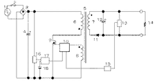
図1に本発明の実施例によるスイッチング電源装置の構成を示す。図において、1はAC入力、2は電流ヒューズ、3はブリッジ整流ダイオード、4は平滑コンデンサである。5はスイッチングトランスで一次巻線6には一方に平滑コンデンサ4の正極が、他方にスイッチング素子9が接続されている。10はスイッチングトランス5の補助巻線8に接続され、スイッチング素子をオンオフするスイッチング制御手段である。11、12はスイッチングトランス5の二次巻線7に接続されスイッチングトランス5の出力を整流・平滑するためのダイオードとコンデンサ、14は出力端子に接続される出力負荷、13は出力電圧を検出するための出力電圧検出手段、15は出力電圧検出手段13の値に応じた制御信号を一次側のスイッチング制御手段10に入力する絶縁信号伝達手段である。 FIG. 1 shows a configuration of a switching power supply apparatus according to an embodiment of the present invention. In the figure, 1 is an AC input, 2 is a current fuse, 3 is a bridge rectifier diode, and 4 is a smoothing capacitor. Reference numeral 5 denotes a switching transformer, to which the positive electrode of the smoothing capacitor 4 is connected to one side of the primary winding 6 and the switching element 9 is connected to the other side. Reference numeral 10 denotes a switching control means which is connected to the auxiliary winding 8 of the switching transformer 5 and turns on / off the switching element. Reference numerals 11 and 12 are connected to the secondary winding 7 of the switching transformer 5 and diodes and capacitors for rectifying and smoothing the output of the switching transformer 5. Reference numeral 14 is an output load connected to the output terminal. Reference numeral 13 is an output voltage. The output voltage detecting means 15 for this is an insulation signal transmitting means for inputting a control signal corresponding to the value of the output voltage detecting means 13 to the switching control means 10 on the primary side.
16は平滑コンデンサ4の正極に接続され、平滑コンデンサ4の電圧を減圧する手段である。17は電圧比較手段であり、入力に減圧手段16の出力電圧と基準電圧18が接続され、その出力はスイッチング制御手段10に接続されている。本発明を実施するには、電圧比較手段17を動作させるための電源電圧や基準電圧18を一次側回路から得る必要がある。それには定電圧源が必要となり、部品を追加しなければない。そこで本実施例では、電圧比較手段17と基準電圧18の機能をスイッチング制御手段10に組み込んだスイッチング制御ICとすることで部品の追加を抑えている。 Reference numeral 16 denotes a means connected to the positive electrode of the smoothing capacitor 4 to reduce the voltage of the smoothing capacitor 4. Reference numeral 17 denotes voltage comparison means, and the output voltage of the decompression means 16 and the reference voltage 18 are connected to the input, and the output is connected to the switching control means 10. In order to implement the present invention, it is necessary to obtain the power supply voltage and the reference voltage 18 for operating the voltage comparison means 17 from the primary side circuit. This requires a constant voltage source and requires additional components. Therefore, in this embodiment, the addition of components is suppressed by using a switching control IC in which the functions of the voltage comparison means 17 and the reference voltage 18 are incorporated in the switching control means 10.
本発明は、上記のように構成されており、AC入力に過電圧が印加されると平滑コンデンサ4の電圧が上昇し、平滑コンデンサ4の電圧を入力とする減圧手段16の出力も上昇する。減圧手段16の出力電圧と基準電圧18を比較し、減圧手段16の出力電圧が基準電圧18よりも大きくなると、電圧比較手段17はスイッチング制御手段10にスイッチングを停止する信号を出力し、スイッチング素子9の動作を停止する。これにより、AC入力が過電圧となったときスイッチング電源装置の動作は停止し、部品の発熱・破損、ヒューズの溶断を防止することができる。 The present invention is configured as described above. When an overvoltage is applied to the AC input, the voltage of the smoothing capacitor 4 increases, and the output of the decompression means 16 that receives the voltage of the smoothing capacitor 4 also increases. When the output voltage of the decompression means 16 is compared with the reference voltage 18 and the output voltage of the decompression means 16 becomes larger than the reference voltage 18, the voltage comparison means 17 outputs a signal for stopping switching to the switching control means 10, and the switching element The operation of 9 is stopped. Thereby, when the AC input becomes an overvoltage, the operation of the switching power supply device is stopped, and it is possible to prevent heat generation / breakage of parts and blowout of the fuse.
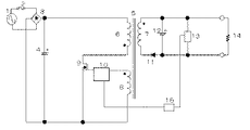
本発明の実施例の回路(図1)と従来例の回路(図2)での過電圧が入力されたときの動作比較を以下の条件で行った。 An operation comparison when an overvoltage was input in the circuit of the embodiment of the present invention (FIG. 1) and the circuit of the conventional example (FIG. 2) was performed under the following conditions.
[条件]
(1)試験は携帯電話用ACアダプタを用いる。
[conditions]
(1) The test uses a mobile phone AC adapter.
(2)図1、図2のスイッチング電源回路にAC100Vを印加し、正常に動作させた後、AC入力を徐々に240Vまで上げていく。 (2) After AC100V is applied to the switching power supply circuit of FIGS. 1 and 2 to operate normally, the AC input is gradually increased to 240V.
(3)スイッチング電源回路が動作中、最も発熱する部品はスイッチング素子9とする。 (3) The switching element 9 is the component that generates the most heat during the operation of the switching power supply circuit.
(4)スイッチング素子9の最大定格電圧Vdsmax=450V、最大動作温度150℃とする。 (4) The maximum rated voltage Vdsmax of the switching element 9 is set to 450 V and the maximum operating temperature is 150 ° C.
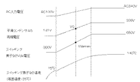
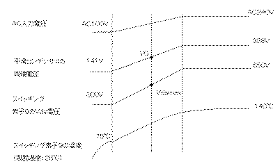
AC入力を上げていったときにスイッチング素子9にかかる電圧Vdsが最大定格電圧Vdsmaxよりも大きくなるときの平滑コンデンサ4の電圧をV0とする。従来例では、図4に示す通り、AC入力を徐々に上げていき平滑コンデンサ4の電圧がV0を超える
と、スイッチング素子9にかかる電圧VdsはVdsmaxより大きくなり、破損する可能性がある。このときスイッチング素子9は140℃まで上昇しており最大動作温度に対して余裕がなく破損の可能性が高くなる。
The voltage of the smoothing capacitor 4 when the voltage Vds applied to the switching element 9 becomes larger than the maximum rated voltage Vdsmax when the AC input is increased is set to V0. In the conventional example, as shown in FIG. 4, when the AC input is gradually increased and the voltage of the smoothing capacitor 4 exceeds V0, the voltage Vds applied to the switching element 9 becomes larger than Vdsmax and may be damaged. At this time, the switching element 9 has risen to 140 ° C., and there is no room for the maximum operating temperature, and the possibility of breakage increases.
しかし、本発明では、入力過電圧保護機能が動作する平滑コンデンサ4の電圧Vovとし、Vov<V0となるように減圧手段16を設定する。図3に示すとおり、スイッチング素子9の最大規格電圧を越える前に、スイッチング動作は停止し、スイッチング素子9にかかる電圧は平滑コンデンサ4と等しくなり、部品の破損を防止できる。さらにこのときスイッチング素子9の温度は80℃までしか上昇せず、スイッチング素子の最大動作温度に対して余裕があり破損の可能性はない。 However, in the present invention, the voltage reducing means 16 is set so that the voltage Vov of the smoothing capacitor 4 at which the input overvoltage protection function operates is Vov <V0. As shown in FIG. 3, the switching operation stops before the maximum standard voltage of the switching element 9 is exceeded, and the voltage applied to the switching element 9 becomes equal to that of the smoothing capacitor 4, thereby preventing damage to the components. Further, at this time, the temperature of the switching element 9 rises only up to 80 ° C., and there is a margin for the maximum operating temperature of the switching element, and there is no possibility of damage.
入力過電圧保護機能を組み込んだスイッチング制御ICにおいて、入力過電圧保護を電流検出と電圧検出で行った場合の検出精度の比較を行った。入力過電圧保護機能を動作させるAC入力を170Vと設定する。このとき、入力過電圧保護機能が動作したAC入力の最小値と最大値を示す。 In the switching control IC incorporating the input overvoltage protection function, the detection accuracy was compared when the input overvoltage protection was performed by current detection and voltage detection. The AC input for operating the input overvoltage protection function is set to 170V. At this time, the minimum value and the maximum value of the AC input in which the input overvoltage protection function operates are shown.
この結果が示すように、過電圧保護電圧は、電圧検出が170V±17V(±10%)であるのに対し、電流検出は170V±60V(±35%)である。電圧検出に比べて電流検出は検出精度が3.5倍となっている。このため、電流検出では精度を上げるための回路の追加が必要になる。 As shown by this result, the overvoltage protection voltage is 170V ± 17V (± 10%) for voltage detection, whereas it is 170V ± 60V (± 35%) for current detection. The detection accuracy of current detection is 3.5 times that of voltage detection. For this reason, in current detection, it is necessary to add a circuit for improving accuracy.
なお、スイッチング素子としてはFETの他、トランジスタなどを用いることができ、回路の設計仕様により選択することができる。また、一次側スイッチング制御機能を有した制御ICに本発明の機能を持たせることも可能である。さらに、減圧手段16における減圧を抵抗による分圧で行うと、過電圧の設定値を容易で安価に設計することができる。 Note that a transistor or the like can be used as the switching element in addition to the FET, and can be selected according to the design specifications of the circuit. It is also possible to give the function of the present invention to a control IC having a primary side switching control function. Furthermore, if the pressure reducing means 16 performs the pressure reduction by dividing the resistance, the overvoltage set value can be designed easily and inexpensively.
本発明は上記のように、AC入力に設定値以上の値が入力されるとスイッチング素子が発振を停止するため、電源の状態が異常であることが容易に分かる。また、過電圧が入力されてもスイッチング素子やヒューズ等の部品の破損、ケースの発熱がないため、修理する必要がなく、製品の信頼性も失われない。 As described above, according to the present invention, it is easily understood that the state of the power supply is abnormal because the switching element stops oscillating when a value greater than the set value is input to the AC input. Even if an overvoltage is input, there is no damage to parts such as switching elements and fuses, and no heat is generated in the case, so there is no need for repair and the reliability of the product is not lost.
1 AC入力
2 電流ヒューズ
3 ブリッジ整流ダイオード
4 平滑コンデンサ
5 スイッチングトランス
6 スイッチングトランス5の一次巻線
7 スイッチングトランス5の二次巻線
8 スイッチングトランス5の補助巻線
9 スイッチング素子(FET)
10 スイッチング制御手段
11 二次側出力整流ダイオード
12 二次側出力平滑コンデンサ
13 出力電圧検出手段
14 出力負荷
15 絶縁信号伝達手段(フォトカプラ)
16 減圧手段
17 電圧比較手段
18 基準電圧
DESCRIPTION OF SYMBOLS 1 AC input 2 Current fuse 3 Bridge rectifier diode 4 Smoothing capacitor 5 Switching transformer 6 Primary winding of switching transformer 7 Secondary winding of switching transformer 5 8 Auxiliary winding of switching transformer 5 9 Switching element (FET)
DESCRIPTION OF SYMBOLS 10 Switching control means 11 Secondary side output rectifier diode 12 Secondary side output smoothing capacitor 13 Output voltage detection means 14 Output load 15 Insulation signal transmission means (photocoupler)
16 Pressure reducing means 17 Voltage comparing means 18 Reference voltage
Claims (3)
Priority Applications (1)
| Application Number | Priority Date | Filing Date | Title |
|---|---|---|---|
| JP2004103807A JP2005295622A (en) | 2004-03-31 | 2004-03-31 | Switching power supply |
Applications Claiming Priority (1)
| Application Number | Priority Date | Filing Date | Title |
|---|---|---|---|
| JP2004103807A JP2005295622A (en) | 2004-03-31 | 2004-03-31 | Switching power supply |
Publications (1)
| Publication Number | Publication Date |
|---|---|
| JP2005295622A true JP2005295622A (en) | 2005-10-20 |
Family
ID=35327960
Family Applications (1)
| Application Number | Title | Priority Date | Filing Date |
|---|---|---|---|
| JP2004103807A Pending JP2005295622A (en) | 2004-03-31 | 2004-03-31 | Switching power supply |
Country Status (1)
| Country | Link |
|---|---|
| JP (1) | JP2005295622A (en) |
Cited By (2)
| Publication number | Priority date | Publication date | Assignee | Title |
|---|---|---|---|---|
| JP2009219316A (en) * | 2008-03-12 | 2009-09-24 | Kyocera Mita Corp | Power supply circuit |
| JPWO2018043226A1 (en) * | 2016-08-30 | 2019-06-24 | パナソニックIpマネジメント株式会社 | Switching power supply device and semiconductor device |
-
2004
- 2004-03-31 JP JP2004103807A patent/JP2005295622A/en active Pending
Cited By (3)
| Publication number | Priority date | Publication date | Assignee | Title |
|---|---|---|---|---|
| JP2009219316A (en) * | 2008-03-12 | 2009-09-24 | Kyocera Mita Corp | Power supply circuit |
| JPWO2018043226A1 (en) * | 2016-08-30 | 2019-06-24 | パナソニックIpマネジメント株式会社 | Switching power supply device and semiconductor device |
| US10651759B2 (en) | 2016-08-30 | 2020-05-12 | Panasonic Intellectual Property Management Co., Ltd. | Switching power supply device and semiconductor device |
Similar Documents
| Publication | Publication Date | Title |
|---|---|---|
| JP4333519B2 (en) | Switching power supply | |
| JP2004088857A (en) | Input overvoltage protection circuit and electric equipment comprising the same | |
| JP2008228538A (en) | Switching power supply | |
| JP2009177990A (en) | Switching power supply device and electrical equipment using the same | |
| US6738247B2 (en) | DC-DC converter | |
| US7558091B2 (en) | Switching power supply apparatus | |
| US20130003239A1 (en) | Switching mode power supply apparatus and power supply method thereof | |
| JP2009189103A (en) | Switching power supply device | |
| JP2009195073A (en) | Switching power supply unit | |
| JP2005295622A (en) | Switching power supply | |
| US20170054285A1 (en) | Protection apparatus for an electrical load, voltage converter comprising a protection apparatus, and method for protecting an electrical load | |
| KR20060130310A (en) | Electronic device and control method | |
| JP2007325428A (en) | Switching power supply | |
| US9906146B2 (en) | Thermal protection circuit for switching power supply | |
| JP2009268227A (en) | Switching power unit | |
| JP2004070709A (en) | Power unit for intrinsically safe apparatus | |
| CN113783430B (en) | Power limiting control circuit and power supply device with same | |
| JP2010148278A (en) | Power circuit with overvoltage protection function, power supply device, image forming apparatus, and method of protection against overvoltage | |
| KR100707400B1 (en) | Electronic ballast for DC voltage with high input voltage and high output current protection circuit | |
| JP2003164054A (en) | Overvoltage protection circuit | |
| JP2009153349A (en) | DC power supply | |
| JP5279219B2 (en) | Switching power supply | |
| JP2010016962A (en) | Switching electric power unit | |
| JP2008109854A (en) | Power supply unit for intrinsically low-cost apparatus | |
| CN119010590A (en) | Power supply device |
Legal Events
| Date | Code | Title | Description |
|---|---|---|---|
| A621 | Written request for application examination |
Free format text: JAPANESE INTERMEDIATE CODE: A621 Effective date: 20070323 |
|
| RD01 | Notification of change of attorney |
Free format text: JAPANESE INTERMEDIATE CODE: A7421 Effective date: 20070412 |
|
| A977 | Report on retrieval |
Free format text: JAPANESE INTERMEDIATE CODE: A971007 Effective date: 20090925 |
|
| A131 | Notification of reasons for refusal |
Free format text: JAPANESE INTERMEDIATE CODE: A131 Effective date: 20091006 |
|
| RD01 | Notification of change of attorney |
Free format text: JAPANESE INTERMEDIATE CODE: A7421 Effective date: 20091120 |
|
| A02 | Decision of refusal |
Free format text: JAPANESE INTERMEDIATE CODE: A02 Effective date: 20100216 |