JP2005295302A - Camera image processing device - Google Patents
Camera image processing device Download PDFInfo
- Publication number
- JP2005295302A JP2005295302A JP2004108944A JP2004108944A JP2005295302A JP 2005295302 A JP2005295302 A JP 2005295302A JP 2004108944 A JP2004108944 A JP 2004108944A JP 2004108944 A JP2004108944 A JP 2004108944A JP 2005295302 A JP2005295302 A JP 2005295302A
- Authority
- JP
- Japan
- Prior art keywords
- image
- feature
- feature pixel
- image data
- pixel
- Prior art date
- Legal status (The legal status is an assumption and is not a legal conclusion. Google has not performed a legal analysis and makes no representation as to the accuracy of the status listed.)
- Pending
Links
Images


Abstract
Description
本発明は、カメラにより連続的に撮像された画像の画質補正に係わり、特に低照度条件下で撮影した画像のノイズ低減に関するものである。 The present invention relates to image quality correction of images continuously captured by a camera, and more particularly to noise reduction of images captured under low illumination conditions.
従来のカメラ画像処理装置は、CCDやC−MOSなどの撮像センサーで光電変換された電気信号を画像処理することで画像データを得ているが、一般に供給電圧の変動や周辺回路の影響によりランダムノイズが発生し、特に低照度条件下で撮影した画像データの場合、その画質劣化が目立つ。このランダムノイズは、注目画素周辺の画素データを使用して平均化することで軽減できるが、この平均化処理を実施すると画像が滑らかになる反面、画像のエッジ情報等の高周波信号成分が失われる。また、対象とする画像データが動画の場合、時間的に連続して取り込んだ画像データを使用することにより同様の平均化処理が可能であるが、たとえ被写体が静止している場合でも、手ぶれ等による画素ずれが生じるため、そのまま平均化等のフィルタ処理を行うと被写体のエッジ部分がぼけてしまう。 A conventional camera image processing apparatus obtains image data by performing image processing on an electrical signal photoelectrically converted by an image sensor such as a CCD or C-MOS, but in general, it is random due to fluctuations in supply voltage or the influence of peripheral circuits. Noise is generated, and particularly in the case of image data taken under low illumination conditions, the image quality deterioration is conspicuous. This random noise can be reduced by averaging using pixel data around the pixel of interest. However, when this averaging process is performed, the image becomes smooth, but high-frequency signal components such as image edge information are lost. . In addition, when the target image data is a moving image, the same averaging process can be performed by using image data captured continuously in time, but even if the subject is stationary, camera shake, etc. As a result of the pixel shift, the edge portion of the subject will be blurred if filter processing such as averaging is performed as it is.
この改善策として、複数のフレーム画像データを用いて画素ずれを補正するものとして、入力される画像に画素レベルでの位置ずれが生じている場合に、関数フィッティングやテンプレートマッチングにより画像の位置合わせを行った後、平均化処理によりランダムノイズを軽減するものがある(例えば、特許文献1参照)。
従来のカメラ画像処理装置では、入力される画像に画素レベルでの位置ずれが生じている場合、関数フィッティングやテンプレートマッチングにより画像の位置合わせを行った後、平均化などのフィルタ処理を施しランダムノイズを軽減することで画像のエッジ部分の画質劣化を抑制していたが、これらの処理が複雑であるため高速化が困難であり、連続して入力される画像データには適さないという問題点があった。 In a conventional camera image processing apparatus, if a positional deviation occurs at the pixel level in an input image, the image is aligned by function fitting or template matching, and then subjected to filter processing such as averaging to generate random noise. The image quality degradation at the edge of the image has been suppressed by reducing the image quality, but it is difficult to increase the speed due to the complexity of these processes, making it unsuitable for continuously input image data. there were.
本発明は、以上のような問題点を解消するためになされたもので、簡単な構成と処理により、特に低照度撮影時において、手ぶれによる画質劣化の少ないノイズ低減が可能なカメラ画像処理装置を提供するものである。 The present invention has been made to solve the above-described problems. A camera image processing apparatus capable of reducing noise with little image quality degradation due to camera shake, particularly in low-light shooting, with a simple configuration and processing. It is to provide.
本発明に係る請求項1のカメラ画像処理装置は、少なくとも入力される第1の画像データおよび第2の画像データを記憶する記憶手段と、前記各画像データに対して微分演算を行う微分手段と、前記微分手段の出力から前記各画像のエッジの強度および向きを算出し、エッジの強度が極大の画素を特徴画素として抽出する特徴画素抽出手段と、前記第1の画像に対応する第1の特徴画素情報を、少なくとも前記特徴画素抽出手段での前記第2の画像に対応する第2の特徴画素情報の検出処理が終了するまで保持する特徴画素情報保持手段と、第1の特徴画素情報と第2の特徴画素情報とが示す特徴画素が同じ画像に関わる特徴画素を表すかどうかを判定し、これらの特徴画素位置情報を出力する特徴画素判定手段と、前記各画像の前記記憶手段への書き込み及び読み出しを制御する記憶制御手段と、前記特徴画素位置情報に基づき、前記第1の画像位置に対する前記第2の画像位置のずれ量を算出する位置情報生成手段と、前記記憶手段から読み出された前記第1の画像データに前記第2の画像データを前記位置ずれ量を補正して重ね合わせ、平均化演算処理によりノイズ低減画像データを得るノイズ低減処理手段とを供えたことを特徴とする。 According to a first aspect of the present invention, there is provided a camera image processing apparatus comprising: storage means for storing at least input first image data and second image data; and differentiation means for performing a differentiation operation on each image data. , Calculating the intensity and direction of the edge of each image from the output of the differentiating means, and extracting a pixel having a maximum edge intensity as a characteristic pixel; and a first corresponding to the first image Feature pixel information holding means for holding feature pixel information until at least the detection process of the second feature pixel information corresponding to the second image in the feature pixel extraction means is completed; and first feature pixel information; Determining whether or not the feature pixel indicated by the second feature pixel information represents a feature pixel related to the same image, and outputting the feature pixel position information; Storage control means for controlling writing to and reading from the position, position information generation means for calculating a shift amount of the second image position with respect to the first image position based on the characteristic pixel position information, and the storage means The second image data is superimposed on the read first image data after correcting the positional deviation amount, and provided with noise reduction processing means for obtaining noise reduced image data by averaging calculation processing. Features.
また、請求項2のカメラ画像処理装置は、請求項1のカメラ画像処理装置において、前記特徴画素抽出手段から出力される特徴画素数を所定の条件に従って制限する特徴画素情報制限手段を備えたことを特徴とする。 According to a second aspect of the present invention, there is provided the camera image processing apparatus according to the first aspect, further comprising characteristic pixel information limiting means for limiting the number of characteristic pixels output from the characteristic pixel extracting means according to a predetermined condition. It is characterized by.
また、請求項3のカメラ画像処理装置は、請求項1のカメラ画像処理装置において、前記位置情報生成手段において算出された前記第1の画像位置に対する前記第2の画像位置のずれ量に、その位置ずれ量により設定される画素数分の位置ずれを付加したことを特徴とする。 According to a third aspect of the present invention, there is provided the camera image processing apparatus according to the first aspect, wherein the second image position shift amount with respect to the first image position calculated by the position information generating means is A positional deviation corresponding to the number of pixels set by the positional deviation amount is added.
この発明のカメラ画像処理装置は、入力画像データを水平及び垂直方向に微分して得られたエッジの強度が極大の画素を特徴画素として抽出し、その特徴画素によりフレーム間の画像のずれ量検出及び画素位置合わせを行い、複数フレームの画像データを用いたノイズ低減処理を行うようにしたので、簡単な構成と処理により、特に手ぶれによる画像の画質劣化を低減できる。 The camera image processing apparatus according to the present invention extracts a pixel having a maximum edge strength obtained by differentiating input image data in the horizontal and vertical directions as a feature pixel, and detects an image shift amount between frames using the feature pixel. In addition, since noise reduction processing using image data of a plurality of frames is performed by performing pixel alignment, deterioration of image quality due to camera shake can be reduced by a simple configuration and processing.
実施の形態1.
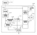
図1はこの発明の実施の形態1であるカメラ画像処理装置の構成を示すブロック図である。同図において、カメラ画像処理装置100は、撮像回路101からフレーム単位で順次入力される画像データのエッジ情報を用いてフレーム間で発生する位置ずれを補正しフィルタ処理を行うものであり、入力される画像データを順次記憶するメモリ105と、メモリ制御信号発生部103および位置情報生成部104からなりメモリ105への書き込みおよび読み出し動作を制御するメモリ制御回路102と、入力される画像データの微分値を算出する微分回路106と、微分回路106の結果からフレーム内での特徴あるエッジ情報をもつ画素を決定する特徴画素抽出回路107と、特徴画素抽出回路107での結果を保持する特徴画素情報保持回路108と、特徴画素抽出回路107の出力と特徴画素情報保持回路108で保持している前フレーム画像データに対する情報から、連続する2つのフレームのそれぞれの特徴画素が同じ特徴点を表すものであるかどうかを判定して現フレームに対してフィルタ処理を行うか否かを決定する特徴画素判定回路109と、複数フレームの画像データを用いてフィルタ処理を行うノイズ低減フィルタ110と、特徴画素判定回路109の結果から現フレームの画像データとノイズ低減フィルタ110の画像データ出力とを選択する選択回路111とから構成されている。
FIG. 1 is a block diagram showing a configuration of a camera image processing apparatus according to
次に、このカメラ画像処理装置100の動作について、図面を用いて説明する。
Next, the operation of the camera
まず、カメラ画像処理装置100の外部にある撮像回路101から、ディジタル画像データがフレーム単位で微分回路106に順次入力されるとともに、メモリ制御回路102から出力される書き込み制御信号および書き込みアドレスに従って、画像データがメモリ105に記憶される。
First, digital image data is sequentially input to the
微分回路106では、入力される画像データに対して1次微分を適用して縦方向および横方向のそれぞれに微分演算を実施し、各画素毎の縦方向微分値と横方向微分値を出力する。ここで縦方向および横方向とは、フレーム画像データの各画素の位置を2次元直交座標系で表した場合のy軸およびx軸の方向に相当する。
The
次に、特徴画素抽出回路107で、フレーム内の画素全てに対して縦方向微分値および横方向微分値の2乗和の平方根、あるいはそれぞれの絶対値の和を算出することでエッジ強度を生成してエッジ強度が極大である特徴画素を抽出し、その特徴画素の位置やエッジ強度および方向を含む特徴画素情報を生成する。ここでの画素位置とは、フレーム画像データの各画素の位置を2次元直交座標系で表した場合のx座標とy座標のことである。エッジ強度が最大となる特徴画素が複数個になる場合も考えられるが、本実施例では、特徴画素がフレームに1つだけあるものとして説明する。
Next, the feature
特徴画素抽出回路107で生成された特徴画素情報は特徴画素情報保持回路108で記憶され、特徴画素抽出回路107での次フレームの画像データに対する処理が完了した時点で、特徴画素抽出回路107の出力とあわせて特徴画素判定回路109に出力される。つまり、2フレーム分の画像データについて、各フレームでの特徴画素情報が特徴画素判定回路109に出力されることになり、特徴画素判定回路109においては特徴画素情報であるエッジ強度および方向のそれぞれについてフレーム間での差分を算出して各フレームで抽出された特徴画素が同じ特徴画素を表すか否かを判定し、同じ特徴画素と判定された場合それら特徴画素間の位置ずれ量と方向を算出し、メモリ制御回路102の位置情報発生部104に出力する。
The feature pixel information generated by the feature
例えば、1番目のフレームとして図2(A)のような画像データが入力され、点線で囲まれた右下隅の画素Paがこのフレームでの特徴あるエッジ情報をもつ画素になるものとし、図2(C)は図2(A)の画素Pa周辺を拡大表示したものである。微分回路106で1番目のフレームの各画素データに対して微分演算を行うことで縦方向微分値および横方向微分値が得られ、特徴画素抽出回路107において各画素でのエッジ強度および方向を算出した結果、画素Paを特徴画素として抽出する。画素Paの縦方向微分値および横方向微分値はそれぞれ、図2(C)での矢印C2および矢印C1になり、エッジの強度は矢印C3の大きさ|C3|で、矢印C3の向きは矢印C1および矢印C2をベクトル加算した結果として表される。このようにして得られる画素Paに関する情報は、次段の特徴画素判定回路109に出力されるとともに特徴画素情報保持回路108へと出力され、次の2番目のフレームに対する特徴画素抽出回路107での同様の動作が完了するまで保持される。
For example, image data as shown in FIG. 2A is input as the first frame, and the pixel Pa in the lower right corner surrounded by a dotted line becomes a pixel having characteristic edge information in this frame. FIG. 2C is an enlarged view of the periphery of the pixel Pa in FIG. The
1番目のフレームについては、特徴画素判定回路109には有効な情報を保持していないため、いったんメモリ105に書き込んでノイズ低減フィルタ110での演算処理はせずに読み出したデータをそのまま出力する、あるいは1フレーム目のデータは出力しないといった特別な処理を行う。
For the first frame, since the effective
2番目のフレームとして図2(B)のような画像データが入力され、右下隅の画素Pbが2番目のフレームでの特徴あるエッジ情報をもつ画素になるものとし、図2(D)は図2(B)の画素Pb周辺を拡大表示したものである。図2(A)での画像の位置は図2(B)における破線の位置に相当し、矢印B1だけ画像位置がずれているものとする。2番目のフレームの画像データに対しても1番目のフレームの場合と同様な処理を実行することで画素Pbが特徴画素として抽出される。画素Pbの縦方向微分値および横方向微分値はそれぞれ図2(D)での矢印D2および矢印D1になり、特徴画素抽出回路107においてエッジ強度は矢印D3の大きさ|D3|で、矢印D3の向きは矢印D1および矢印D2をベクトル加算した結果として表される。
Image data as shown in FIG. 2B is input as the second frame, and the pixel Pb in the lower right corner becomes a pixel having characteristic edge information in the second frame, and FIG. 2 (B) is an enlarged display around the pixel Pb. The position of the image in FIG. 2A corresponds to the position of the broken line in FIG. 2B, and the image position is shifted by the arrow B1. The pixel Pb is extracted as a feature pixel by executing the same process as that of the first frame for the image data of the second frame. The vertical differential value and the horizontal differential value of the pixel Pb are respectively an arrow D2 and an arrow D1 in FIG. 2D, and the edge intensity in the feature
特徴画素判定回路109には、2番目のフレームの処理時に特徴画素情報保持回路108からは画素Paの、特徴画素抽出回路107からは画素Pbの、画素位置とエッジ強度および方向の情報が入力され、これら2つの画素について、エッジ強度の差分(|D3|−|C3|)およびエッジ方向の差{(D1+D2)−(C1+C2)}を算出し、例えばそれぞれがあらかじめ設定してある閾値の範囲内である場合、画素PaおよびPbは同じ特徴をもつ画素でそれぞれのフレームにおいて同一の画素を表すと判定し、エッジ強度の差分及び方向の差が閾値の範囲を越えている場合、画素PaおよびPbは異なる特徴を持ち、相関のない画素であると判定する。
The pixel position, edge strength, and direction information of the pixel Pa from the feature pixel
画素間の相関の判断基準は、あらかじめ設定しておいても、外部から設定可能な構成としておいてもよい。 The criterion for determining the correlation between the pixels may be set in advance or may be set from the outside.
画素Pa、Pbが同一画素であると判定された場合、画像データが図2(B)の矢印B1で表される画素数および方向にずれていると考えられる。画素Pa、Pbの位置情報からx方向およびy方向のそれぞれについての画素数のずれ量、つまり矢印B1のx成分Bxおよびy成分Byを算出し、その結果をメモリ制御回路102へと出力する。メモリ制御回路102では、メモリ105から2番目のフレームの画像データ読み出す際に1番目のフレームに対して読み出し開始アドレスにx方向にBx画素、y方向にBy画素だけオフセットを持たせるように位置情報生成部104においてメモリ制御用のアドレスを生成し、制御信号発生部103では位置情報生成部104の出力に同期してチップセレクト信号やアウトプットイネーブル信号といった実際にメモリを制御する信号生成することでメモリ105を制御し、フレーム間での画素位置のずれを補正する。
When it is determined that the pixels Pa and Pb are the same pixel, it is considered that the image data is shifted in the number and direction of pixels represented by the arrow B1 in FIG. The shift amount of the number of pixels in each of the x direction and the y direction, that is, the x component Bx and the y component By of the
つまりメモリ105に記憶している1フレーム目の画像データのうち、図2(E)の太線で囲まれた領域Raのデータのみを読み出して出力するとすれば、2フレーム目の画像データとしては図2(E)の領域Raから矢印B1だけ平行移動した、図2(F)で太線で囲まれた領域Rbのデータを読み出すことになる。
That is, if only the data in the area Ra surrounded by the thick line in FIG. 2E is read and output from the image data of the first frame stored in the
したがって、画素の位置ずれを補正可能な範囲は、メモリ105に記憶できる画像データの画素数およびカメラ画像処理装置100から出力する画像データのフレーム画素数等により制限される。
Therefore, the range in which the pixel position deviation can be corrected is limited by the number of pixels of image data that can be stored in the
次にノイズ低減フィルタ110では、メモリ105に記憶している画像データを読み出して、例えば連続する2フレームの画像データに対して加算平均をとるといったノイズを低減する処理を行う。
Next, the
選択回路111では、特徴画素判定回路109での判定結果に従って、画素Pa、Pbに相関がないと判定した場合はメモリ105から読み出した画像データそのものを、画素Pa、Pbは同じ特徴画素であると判定した場合はメモリ105から読み出した画像データに対し演算処理を施したノイズ低減フィルタ110の出力画像データを選択して出力する。
When the selection circuit 111 determines that there is no correlation between the pixels Pa and Pb according to the determination result of the feature
以上の処理をフレーム画像データが入力される毎に繰り返し実行する。ただし、3フレーム目以降のデータに対しては、1つ前のフレームに対する処理の際に特徴画素判定回路109において特徴画素が同一の画像構成要素であると判定してメモリ105からの画像データの読み出しアドレスを補正している場合、特徴画素情報保持回路108で保持している特徴画素の位置情報は1つ前のフレームで読み出しアドレスに対して補正した分のずれを含んでいることになるため、補正後の位置情報に差し換えて特徴画素判定回路109での処理に使用する必要がある。
The above process is repeated every time frame image data is input. However, for the data of the third and subsequent frames, the feature
なお、本実施の形態では、連続する2フレーム分の画像データに対する処理として説明したが、メモリ105の容量および書き込み読み出しに必要な時間に制限されなければ、3フレーム分以上の画像データに対しても同様な処理を実行可能なように構成することもできる。
Although the present embodiment has been described as processing for image data for two consecutive frames, if the capacity of the
上述した処理により、順次入力される画像データに対する画素ずれを補正した上でフィルタ演算を実行することになり、画像のエッジ周辺部分のぼけを最低限に抑えることができる。 With the processing described above, the pixel calculation for the sequentially input image data is corrected, and the filter operation is executed, so that the blur around the edge of the image can be minimized.
実施の形態2.
図3はこの発明装置の実施の形態2の構成を示すブロック図である。このカメラ画像処理装置200において、図1に示したカメラ画像処理装置100と同様の部分については同一の符号を付しており、特徴画素抽出回路107と特徴画素判定回路109の間に、特徴画素フィルタ201を設けている点が異なる。特徴画素フィルタ201は、特徴画素抽出回路107において複数の特徴画素を抽出した場合に、設定された特定の条件に従って後段回路に出力する特徴画素数を制限するものである。以下にカメラ画像処理装置200の具体的な動作について説明する。
Embodiment 2. FIG.
FIG. 3 is a block diagram showing the configuration of Embodiment 2 of the inventive device. In this camera
特徴画素抽出回路107で複数の画素が抽出された場合、その特徴画素の全ての情報を次段の回路に出力すると、特徴画素情報保持回路108では抽出された特徴画素数分の情報を保持する回路が必要になり、特徴画素判定回路109では抽出された特徴画素数と同じ回数の判定処理を実行する必要がある。そのための実行時間あるいは並列処理するための回路が必要となるが、これら回路規模や処理時間は、入力されるフレーム画像データの総画素数が多くなるほど増大することになる。
When a plurality of pixels are extracted by the feature
本実施の形態では、特徴画素フィルタ201において、例えばフレーム内で最後の特徴画素のみを用いるといった条件を設定して抽出された複数の特徴画素からさらに制限した情報を後段回路での処理に用いることで、回路規模や処理時間の増大を抑制できるとともに、入力されるフレーム画像データの総画素数に依存しない回路を構成することが可能となる。
In the present embodiment, in the
なお、特徴画素フィルタ201に設定するフィルタ条件は、あらかじめ設定しておいても、外部から設定可能な構成しておいてもよい。
Note that the filter conditions set in the
実施の形態3.
図4はこの発明装置の実施の形態3の構成を示すブロック図である。このカメラ画像処理装置300において、図1に示したカメラ画像処理装置100と同様の部分については同一の符号を付しており、メモリ制御回路102の位置情報生成部104の代わりに、エッジ強調処理用位置情報生成部301を用いている点が異なる。以下にカメラ画像処理装置300の具体的な動作について説明する。
Embodiment 3 FIG.
FIG. 4 is a block diagram showing the configuration of Embodiment 3 of the inventive device. In this camera
カメラ画像処理装置100の位置情報生成部104では、連続して入力される画像データのエッジが一致するようにアドレス発生を制御していたが、ノイズ低減フィルタ110において画像データの内容によらず一様にノイズの低減処理を行うとエッジ部分がぼける。そこでエッジ強調処理用位置情報生成部301を用いて、ノイズ低減フィルタ110で処理を行う複数フレームの画像データを重ね合わせた時に画像の輪郭が上下左右のいずれかの方向に1画素程度ずれるようにメモリ105からの画像データ読み出しアドレスを制御することでエッジ部分の強調処理と同様な効果が得られ、ノイズ低減フィルタ110での画像のエッジ周辺部分のぼけを抑制することができる。
In the position
なお、エッジ強調処理用位置情報生成部301でずらす画素数や方向については、あらかじめ固定としても、外部から設定可能な構成としてもよい。
Note that the number and direction of pixels shifted by the edge enhancement processing position
100 カメラ画像処理装置、101 撮像回路、102 メモリ制御回路、103 メモリ制御信号発生部、104 位置情報生成部、105 メモリ、106 微分回路、
107 特徴画素抽出回路、108 特徴画素情報保持回路、109 特徴画素判定回路、110 ノイズ低減フィルタ、111 選択回路。
DESCRIPTION OF
107 feature pixel extraction circuit, 108 feature pixel information holding circuit, 109 feature pixel determination circuit, 110 noise reduction filter, 111 selection circuit.
Claims (3)
少なくとも入力される第1の画像データおよび第2の画像データを記憶する記憶手段と、
前記各画像データに対して微分演算を行う微分手段と、
前記微分手段の出力から前記各画像のエッジの強度および向きを算出し、エッジの強度が極大の画素を特徴画素として抽出する特徴画素抽出手段と、
前記第1の画像に対応する第1の特徴画素情報を、少なくとも前記特徴画素抽出手段での前記第2の画像に対応する第2の特徴画素情報の検出処理が終了するまで保持する特徴画素情報保持手段と、
第1の特徴画素情報と第2の特徴画素情報とが示す特徴画素が同じ画像に関わる特徴画素を表すかどうかを判定し、これらの特徴画素位置情報を出力する特徴画素判定手段と、
前記各画像の前記記憶手段への書き込み及び読み出しを制御する記憶制御手段と、
前記特徴画素位置情報に基づき、前記第1の画像位置に対する前記第2の画像位置のずれ量を算出する位置情報生成手段と、
前記記憶手段から読み出された前記第1の画像データに前記第2の画像データを前記位置ずれ量を補正して重ね合わせ、平均化演算処理によりノイズ低減画像データを得るノイズ低減処理手段とを供えたことを特徴とするカメラ画像処理装置。 In a camera image processing apparatus that performs image processing on digital image data obtained by camera photography,
Storage means for storing at least input first image data and second image data;
Differentiating means for performing a differentiation operation on each image data,
Calculating the intensity and direction of the edge of each image from the output of the differentiating means, and extracting a pixel having a maximum edge intensity as a characteristic pixel;
Feature pixel information for holding first feature pixel information corresponding to the first image until at least the detection processing of the second feature pixel information corresponding to the second image in the feature pixel extraction unit is completed Holding means;
Feature pixel determination means for determining whether or not the feature pixels indicated by the first feature pixel information and the second feature pixel information represent feature pixels related to the same image, and outputting the feature pixel position information;
Storage control means for controlling writing and reading of each image to the storage means;
Position information generating means for calculating a shift amount of the second image position with respect to the first image position based on the characteristic pixel position information;
Noise reduction processing means for correcting the positional deviation amount and superimposing the second image data on the first image data read from the storage means and obtaining noise reduced image data by averaging calculation processing; A camera image processing apparatus characterized by being provided.
The positional deviation corresponding to the number of pixels set by the positional deviation amount is added to the deviation amount of the second image position with respect to the first image position calculated by the positional information generation unit. Item 2. The camera image processing device according to Item 1.
Priority Applications (1)
| Application Number | Priority Date | Filing Date | Title |
|---|---|---|---|
| JP2004108944A JP2005295302A (en) | 2004-04-01 | 2004-04-01 | Camera image processing device |
Applications Claiming Priority (1)
| Application Number | Priority Date | Filing Date | Title |
|---|---|---|---|
| JP2004108944A JP2005295302A (en) | 2004-04-01 | 2004-04-01 | Camera image processing device |
Publications (1)
| Publication Number | Publication Date |
|---|---|
| JP2005295302A true JP2005295302A (en) | 2005-10-20 |
Family
ID=35327732
Family Applications (1)
| Application Number | Title | Priority Date | Filing Date |
|---|---|---|---|
| JP2004108944A Pending JP2005295302A (en) | 2004-04-01 | 2004-04-01 | Camera image processing device |
Country Status (1)
| Country | Link |
|---|---|
| JP (1) | JP2005295302A (en) |
Cited By (6)
| Publication number | Priority date | Publication date | Assignee | Title |
|---|---|---|---|---|
| JP2007281546A (en) * | 2006-04-03 | 2007-10-25 | Samsung Techwin Co Ltd | Imaging apparatus and imaging method |
| KR100810154B1 (en) | 2006-06-28 | 2008-03-06 | 엠텍비젼 주식회사 | Apparatus and method for removing noise of image |
| KR100866963B1 (en) | 2007-03-12 | 2008-11-05 | 삼성전자주식회사 | Method for stabilizing digital image which can correct the horizontal shear distortion and vertical scale distortion |
| KR100888428B1 (en) | 2007-02-08 | 2009-03-11 | 엠텍비젼 주식회사 | Device and Method of Removing Noise of Image |
| US7773825B2 (en) | 2005-11-02 | 2010-08-10 | Nec Electronics Corporation | Image stabilization apparatus, method thereof, and program product thereof |
| JP2012514419A (en) * | 2008-12-30 | 2012-06-21 | インテル・コーポレーション | Method and apparatus for reducing noise in video |
-
2004
- 2004-04-01 JP JP2004108944A patent/JP2005295302A/en active Pending
Cited By (9)
| Publication number | Priority date | Publication date | Assignee | Title |
|---|---|---|---|---|
| US7773825B2 (en) | 2005-11-02 | 2010-08-10 | Nec Electronics Corporation | Image stabilization apparatus, method thereof, and program product thereof |
| JP2007281546A (en) * | 2006-04-03 | 2007-10-25 | Samsung Techwin Co Ltd | Imaging apparatus and imaging method |
| US7856174B2 (en) | 2006-04-03 | 2010-12-21 | Samsung Electronics Co., Ltd. | Apparatus and method for image pickup |
| JP4662880B2 (en) * | 2006-04-03 | 2011-03-30 | 三星電子株式会社 | Imaging apparatus and imaging method |
| KR100810154B1 (en) | 2006-06-28 | 2008-03-06 | 엠텍비젼 주식회사 | Apparatus and method for removing noise of image |
| KR100888428B1 (en) | 2007-02-08 | 2009-03-11 | 엠텍비젼 주식회사 | Device and Method of Removing Noise of Image |
| KR100866963B1 (en) | 2007-03-12 | 2008-11-05 | 삼성전자주식회사 | Method for stabilizing digital image which can correct the horizontal shear distortion and vertical scale distortion |
| JP2012514419A (en) * | 2008-12-30 | 2012-06-21 | インテル・コーポレーション | Method and apparatus for reducing noise in video |
| US8903191B2 (en) | 2008-12-30 | 2014-12-02 | Intel Corporation | Method and apparatus for noise reduction in video |
Similar Documents
| Publication | Publication Date | Title |
|---|---|---|
| JP4487191B2 (en) | Image processing apparatus and image processing program | |
| US10636126B2 (en) | Image processing device, imaging apparatus, image processing method, image processing program, and recording medium | |
| JP5569357B2 (en) | Image processing apparatus, image processing method, and image processing program | |
| JP2010166558A (en) | Image forming apparatus | |
| TWI496105B (en) | Image synthesis device and computer program for image synthesis | |
| JP2010211255A (en) | Imaging apparatus, image processing method, and program | |
| JP2015186247A (en) | Image processing system, control method, and program | |
| JP2017175364A (en) | Image processing device, imaging device, and control method of image processing device | |
| JP2018207413A (en) | Imaging apparatus | |
| JP2022179514A (en) | Control apparatus, imaging apparatus, control method, and program | |
| JP6541501B2 (en) | IMAGE PROCESSING APPARATUS, IMAGING APPARATUS, AND IMAGE PROCESSING METHOD | |
| JP6564284B2 (en) | Image processing apparatus and image processing method | |
| JP2006325274A (en) | Imaging device | |
| JP2005295302A (en) | Camera image processing device | |
| JP4418342B2 (en) | Image processing apparatus and electronic camera | |
| JP2009049575A (en) | Image processing device, image processing method, and program | |
| JP5760654B2 (en) | Image processing apparatus, image processing method, and program | |
| JPH1117984A (en) | Image processor | |
| JP7442989B2 (en) | Imaging device, control method for the imaging device, and program | |
| JP2010056817A (en) | Imaging apparatus | |
| JP2008235958A (en) | Imaging apparatus | |
| JP2017055309A (en) | Imaging apparatus and its control method | |
| JP5477897B2 (en) | Image motion correction apparatus and method, and imaging apparatus | |
| CN110913143B (en) | Image processing method, image processing device, storage medium and electronic equipment | |
| JP2018098612A (en) | Image processing system, image processing method, imaging apparatus, program, and storage medium |
Legal Events
| Date | Code | Title | Description |
|---|---|---|---|
| A977 | Report on retrieval |
Free format text: JAPANESE INTERMEDIATE CODE: A971007 Effective date: 20080109 |
|
| A131 | Notification of reasons for refusal |
Free format text: JAPANESE INTERMEDIATE CODE: A131 Effective date: 20080115 |
|
| A521 | Request for written amendment filed |
Free format text: JAPANESE INTERMEDIATE CODE: A523 Effective date: 20080314 |
|
| A131 | Notification of reasons for refusal |
Free format text: JAPANESE INTERMEDIATE CODE: A131 Effective date: 20090317 |
|
| A521 | Request for written amendment filed |
Free format text: JAPANESE INTERMEDIATE CODE: A523 Effective date: 20090515 |
|
| A02 | Decision of refusal |
Free format text: JAPANESE INTERMEDIATE CODE: A02 Effective date: 20090915 |