JP2005295093A - Line light source and image sensor - Google Patents
Line light source and image sensor Download PDFInfo
- Publication number
- JP2005295093A JP2005295093A JP2004105676A JP2004105676A JP2005295093A JP 2005295093 A JP2005295093 A JP 2005295093A JP 2004105676 A JP2004105676 A JP 2004105676A JP 2004105676 A JP2004105676 A JP 2004105676A JP 2005295093 A JP2005295093 A JP 2005295093A
- Authority
- JP
- Japan
- Prior art keywords
- light
- light source
- light guide
- line
- line light
- Prior art date
- Legal status (The legal status is an assumption and is not a legal conclusion. Google has not performed a legal analysis and makes no representation as to the accuracy of the status listed.)
- Granted
Links
Images

Landscapes
- Facsimile Heads (AREA)
- Facsimile Scanning Arrangements (AREA)
- Light Sources And Details Of Projection-Printing Devices (AREA)
Abstract
【課題】 導光体を用いたライン光源において、構造起因による発光不均一性を改善するライン光源を提供する。
【解決手段】 導光体カバー2に覆われた透明な部材からなる導光体3と、近傍に位置する光源1と、その光源1から照射された光を上記導光体3に入光させ、導光体3に描かれた拡散部4によって光を拡散させる構造を持つライン光源において、部品構造による不可避の照明不均一性を生じさせる場合において、その不均一を生じさせている個所に、光を制御するための拡散部4をたとえば塗料35を塗布することで、照明均一性を改善することができるようにしたものである。
【選択図】 図1
PROBLEM TO BE SOLVED: To provide a line light source for improving light emission nonuniformity due to a structure in a line light source using a light guide.
SOLUTION: A light guide 3 made of a transparent member covered with a light guide cover 2, a light source 1 located in the vicinity, and light emitted from the light source 1 is incident on the light guide 3. In a line light source having a structure in which light is diffused by the diffusing unit 4 drawn on the light guide 3, in the case where inevitable illumination non-uniformity is caused by the component structure, the non-uniformity is caused in The illumination uniformity can be improved by applying, for example, a paint 35 to the diffusion portion 4 for controlling light.
[Selection] Figure 1
Description
本発明は複写機、ファクシミリなどの画像を読み取る画像入力装置に用いられる密着イメージセンサ用のライン光源及びこれを用いたイメージセンサに関するものである。 The present invention relates to a line light source for a contact image sensor used in an image input apparatus for reading an image such as a copying machine and a facsimile, and an image sensor using the line light source.
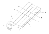
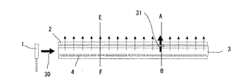
原稿などの画像情報を読み取る密着イメージセンサに使用されるライン光源として、例えば特開平8−163320号公報に開示されたものがある。以下、図を用いて従来のライン光源について説明する。図4はライン光源全体の斜視図である。図5はライン光源に用いられているLEDの発光部である。図6は図4におけるライン光源のEF断面図である。図7は図4におけるライン光源の長手方向の側面図である。 As a line light source used for a contact image sensor for reading image information such as a document, there is one disclosed in, for example, Japanese Patent Laid-Open No. 8-163320. Hereinafter, a conventional line light source will be described with reference to the drawings. FIG. 4 is a perspective view of the entire line light source. FIG. 5 shows a light emitting part of an LED used for a line light source. 6 is an EF cross-sectional view of the line light source in FIG. FIG. 7 is a side view of the line light source in FIG. 4 in the longitudinal direction.
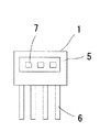
従来のライン光源は、LED発光部1を発光源としている。LED発光部1は、リードフレームと呼ばれる電極端子6を有し、実装基板5にLED(LIGHT EMITTED DIODE)チップ7と呼ばれる半導体発光素子を実装した構造となっている。上記実装基板5は、インサート成型と呼ばれる手法を用いて作製される。LED発光部1から照射された光30を導光体カバー2で覆われた透明な部材からなる導光体3に入光させる。この光は全反射角を維持しながら、導光体3を進行し、拡散部4と呼ばれる反射率60%以上を有する入射光を拡散反射する拡散部にあたって拡散光9となる。光出射面8からその拡散光9が照射される構造となっている。
The conventional line light source uses the LED
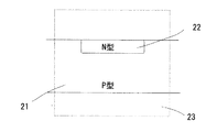
このようなライン光源をイメージセンサに用いた場合、イメージセンサの出力強度Iは、イメージセンサに使用するセンサICの感度S、ライン光源の光量B及び読取速度Tの積に比例する。したがって、これらのパラメータにより、I∝S×B×T と表すことができる。イメージセンサを高速に動作させるには、ライン光源の光量Bを大きくする必要がある。また、センサICの感度を大きくするためには、図8に示すように、センサICに実装されるP型半導体21とN型半導体22の接合によって構成されるフォトダイオード23の構成(図8参照)を考慮する必要がある。センサICは、上記フォトダイオード23と信号処理部(図示せず)とから構成される。
When such a line light source is used for the image sensor, the output intensity I of the image sensor is proportional to the product of the sensitivity S of the sensor IC used for the image sensor, the light amount B of the line light source, and the reading speed T. Therefore, these parameters can be expressed as I∝S × B × T. In order to operate the image sensor at high speed, it is necessary to increase the light quantity B of the line light source. Further, in order to increase the sensitivity of the sensor IC, as shown in FIG. 8, a configuration of a photodiode 23 formed by joining a P-
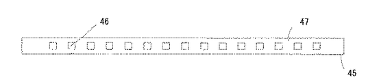
しかし、汎用のLSI半導体作製工程によって作製されたフォトダイオードの感度向上には限界がある。半導体の光電変換効率を飛躍的に向上させるには、CCDセンサー等のイメージセンサー用半導体作製工程を選択する必要があり、コスト的に問題点が多い。また、ライン光源の光量Bを大きくする方式として、図9に示すように、LEDチップ46の数量を増やし、それらを等間隔に基板47上に配置し、輝度向上を狙ったLEDアレイ方式45が一般的に知られている。しかし、この方式においてはLEDチップの製造上のばらつきにより、LED輝度がばらつく。その結果、照明ばらつきが生じ、LEDチップ実装間隔とLEDの発光指向性によっては、照射面における照明の均一性が悪化するという問題がある。
However, there is a limit to improving the sensitivity of a photodiode manufactured by a general-purpose LSI semiconductor manufacturing process. In order to dramatically improve the photoelectric conversion efficiency of a semiconductor, it is necessary to select a semiconductor manufacturing process for an image sensor such as a CCD sensor, which is problematic in terms of cost. Further, as a method of increasing the light amount B of the line light source, as shown in FIG. 9, there is an
そこで、図4に示すような構成のライン光源を用い、より高輝度なLEDチップを使用することで高輝度かつ均一性を有するライン光源とする試みが行われている。発光部1で照射された光は導光体3に入光し、拡散部4にあたると減衰する。したがってライン光源の照明均一性を得るために、拡散部4を、入光面近くから遠くなるにつれて、「疎の状態」から「密の状態」、または、「細い状態」から「太い状態」となるように構成する。つまり、LED発光部1に近い側(光の強度が強いところ)では、拡散部4の密度(拡散部が設けられる導光体側面の単位面積当りの拡散部正味の面積)が低く、LED発光部1から遠い側(光の強度が弱いところ)では、拡散部4の密度が高くなっている。このような構成とすることにより、入射面から遠いところで光をより拡散させることが可能となり、照明均一性を得ている。
Therefore, an attempt has been made to obtain a line light source having high brightness and uniformity by using a line light source having a configuration as shown in FIG. 4 and using a higher brightness LED chip. The light emitted from the
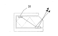
導光体3はコストが比較的安価な樹脂からなる透明部材からなっている。たとえば、アクリルなどである。アクリルなどの樹脂成型品においては製品の金型をもちい、その金型に高温に加熱された樹脂材料を圧力をかけて注入し、その後冷却して製品を製作する。このとき、金型に樹脂材料を注入する流路部分は一般的にゲートと呼ばれている。樹脂成形直後では、製品本体の形状と共にこの流路形状(上記金型ゲートに対応するゲート部31)が一体形状として成形される。そのため、鋭利なナイフ等でこの流路(ゲート部31)を切断している。
The
このゲート部31の表面は、ナイフ等で切断されていることから表面の平坦性が悪い不均一な領域となっている。通常、導光体は光を効率よく全反射角を維持できるよう導光するために、凹凸のない面で構成されている。この平坦性の悪化した部分に、導光された光が照射されると、全反射することなく散乱する。この散乱光は拡散部4と同様の役割を果たし、照明均一性に10〜20%程度影響を与えることとなる。図10は、ゲート部31を有するAB断面図を示すものである。ゲート部31によって散乱光が発生し、この散乱光が出射される。図7は図4におけるライン光源の側面発光強度の模式図を示す。図にしめすとおり、このAB断面の発光強度はEF断面の発光強度に比べ、10〜20%程度変動し、均一性を悪化させる。このため、導光体のゲート部は、光源から最も離れた、照明均一性に影響の少ない場所に作製されるのが一般的である。しかし、上記のとおりゲート部31の作製位置の制約を受けるため、樹脂成型において安定な場所にゲートを作製することができず、樹脂注入がしづらく成型条件が不安定になり、歩留まりを低下させる原因となっている。
Since the surface of the
請求項1に係るライン光源は、長手方向の側面に光出射面を形成した導光体と、この導光体の端部に配置され、上記導光体に光を入射する光源と、上記光出射面を形成した側面を除く上記導光体の側面を覆うカバーと、このカバーで覆われた上記導光体の一の側面に離散的に設けられ、上記入射光を拡散反射する拡散部と、この拡散部の設けられた側面とは異なる他の側面の所定領域に設けられ、上記入射光を吸収する吸収部とを備えたことを特徴とするものである。 According to a first aspect of the present invention, there is provided a line light source including a light guide having a light emitting surface formed on a side surface in a longitudinal direction, a light source disposed at an end of the light guide, and incident light on the light guide, and the light. A cover that covers a side surface of the light guide body excluding a side surface on which an emission surface is formed; a diffusion unit that is discretely provided on one side surface of the light guide body covered with the cover and diffuses and reflects the incident light; And an absorption portion that is provided in a predetermined region on another side surface different from the side surface on which the diffusion portion is provided and absorbs the incident light.
また、請求項2に係るイメージセンサは、相対して設けられた請求項1に記載の第1及び第2のライン光源と、このライン光源からの光が原稿により反射され、その反射光を集光するロッドレンズアレイと、このロッドレンズアレイにより集光された反射光を検出するセンサICとを備えたことを特徴とするものである。 According to a second aspect of the present invention, there is provided the image sensor according to the first aspect, wherein the first and second line light sources according to the first aspect and the light from the line light source are reflected by the document, and the reflected light is collected. A rod lens array that emits light and a sensor IC that detects reflected light collected by the rod lens array are provided.
請求項1に係るライン光源は、高輝度かつ均一性を持った光源を提供できる。また、請求項2に係るイメージセンサは、請求項1に記載のライン光源を用いるので、読み取りばらつきのない良好な画像情報を読み取ることができ、良好な読取特性を有するスキャナー、複写機等の画像入力装置を提供できる。
The line light source according to
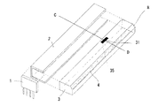
実施例1.
本発明のライン光源は、ゲート部31における光散乱を低減することができるものである。図1に、本発明のライン光源の斜視図を示す。図において、LED発光部1の構成は図5に示すものと同様であり説明を省略する。導光体3はアクリル等を材料とする樹脂成形品により製造され、断面5角形の柱状形態を有している。導光体カバー2は、白色の樹脂材を材料とし、断面コの字形状を有し、導光体3の所定の3側面(図では光の出射面8を除く3つの側面)を覆う構造となっている。この導光体カバー2は、導光体3の内面で全反射せず突き抜けてくる光を導光体3内に再反射し戻す機能を有する。また、外部から導光体3への雑音光の侵入を防止する補助的役目も果たす。
Example 1.
The line light source of the present invention can reduce light scattering in the
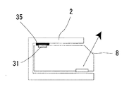
ゲート部31には、反射率の低い塗料、例えば、黒の色彩をもつ反射防止用の塗料35を塗布している。上記塗料35を塗布すると、ゲート部31からの散乱光の発生を塗料35が吸収抑制する。図2は、図1におけるライン光源のCD断面図を示す。図に示すように、CD断面の発光分布はEF断面(図4)と同一の発光分布を有することができ、光分布の均一なライン光源を提供することができる。導光体3に散乱光を発生する箇所が存在する場合、上記と同様の手法を用いることで、ライン光源の照明均一性を改善し、良好な光源を提供することができる。
The
なお、上記説明では、ゲート部31は、拡散部4の設けられた側面と相対する側面に設けられている場合について説明したが、これに限られるものではない。例えば、LED発光部1が設置されている導光体3の一端とは反対側の他端の面に設けることも可能である。この場合にもゲート部31を覆うように塗料35を塗布しゲート部からの散乱光を抑制する必要がある。
In the above description, the case where the
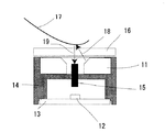
次に、図3により本発明のイメージセンサについて説明する。イメージセンサは、上記ライン光源11と光電変換を行うセンサIC12と呼ばれる半導体、センサIC12を実装するための基板13、ライン光源から照射された光を集光するレンズ15、透明な部材からなる平面を有する透明板16、及びこれらの構成部品12、13、15、及び16を保持する筐体14から構成されている。図に示すように、ライン光源11は相対する要に配置されている。これは、原稿17に両側から光を照射し、原稿の皺などにより影部分ができないようにするためである。レンズ15は、複数個のロッドレンズ(図示せず)によって構成された正立等倍結像用の、いわゆるロッドレンズアレイにより構成されている。イメージセンサは、ライン光源11から照射された光18が原稿17にあたり、その反射光19をレンズ15によって集光し、それをセンサIC12によって光電変換を行い、それを画像情報として出力する。
Next, the image sensor of the present invention will be described with reference to FIG. The image sensor has a plane made up of a semiconductor called a
1 LED発光部、 2 導光体カバー、 3 導光体、 4 拡散部、 5 LED実装基板、 6 LED発光部電極端子、 7 LEDチップ、 8 導光体照射面(出射面)、 9 拡散光、 11 ライン光源、 12 センサIC、 13 基板、 14 筐体、 15 レンズ、 16 透明板、 17 原稿、 18 照射光、 19 原稿反射光、 21 P型半導体、 22 N型半導体、 23 フォトダイオード、 31 ゲート部、 32 拡散部、 35 拡散防止塗料、 45 LEDアレイ光源、 46 LEDチップ、 47 基板。
DESCRIPTION OF
Claims (2)
2. The first and second line light sources according to claim 1, which are provided relative to each other, and a rod lens array in which light from the first and second line light sources is reflected by a document and the reflected light is collected. And a sensor IC for detecting reflected light collected by the rod lens array.
Priority Applications (1)
| Application Number | Priority Date | Filing Date | Title |
|---|---|---|---|
| JP2004105676A JP4259377B2 (en) | 2004-03-31 | 2004-03-31 | Line light source and image sensor |
Applications Claiming Priority (1)
| Application Number | Priority Date | Filing Date | Title |
|---|---|---|---|
| JP2004105676A JP4259377B2 (en) | 2004-03-31 | 2004-03-31 | Line light source and image sensor |
Publications (2)
| Publication Number | Publication Date |
|---|---|
| JP2005295093A true JP2005295093A (en) | 2005-10-20 |
| JP4259377B2 JP4259377B2 (en) | 2009-04-30 |
Family
ID=35327564
Family Applications (1)
| Application Number | Title | Priority Date | Filing Date |
|---|---|---|---|
| JP2004105676A Expired - Lifetime JP4259377B2 (en) | 2004-03-31 | 2004-03-31 | Line light source and image sensor |
Country Status (1)
| Country | Link |
|---|---|
| JP (1) | JP4259377B2 (en) |
Cited By (5)
| Publication number | Priority date | Publication date | Assignee | Title |
|---|---|---|---|---|
| ITTO20090998A1 (en) * | 2009-12-17 | 2011-06-18 | Cts Cashpro Spa | IMAGE CONTACT SENSOR AND METHOD TO IMPROVE THE RESPONSE OF A CONTACT IMAGE SENSOR, IN PARTICULAR FOR BANKNOTE SCANNING. |
| JP2011234150A (en) * | 2010-04-28 | 2011-11-17 | Panasonic Corp | Light guide body, and illuminator and document reader equipped with the same |
| US8570616B2 (en) | 2010-06-04 | 2013-10-29 | Kabushiki Kaisha Toshiba | Lighting device, image reading device, and image forming apparatus |
| JP2014033440A (en) * | 2012-07-13 | 2014-02-20 | Canon Components Inc | Illumination device, image sensor unit, image reading device, and image forming apparatus |
| US10459156B2 (en) | 2017-10-24 | 2019-10-29 | Canon Kabushiki Kaisha | Light guiding member and illumination device |
Citations (7)
| Publication number | Priority date | Publication date | Assignee | Title |
|---|---|---|---|---|
| JPS61258718A (en) * | 1985-05-10 | 1986-11-17 | Matsushita Electric Ind Co Ltd | Plastic optical apparatus |
| JPS63179728A (en) * | 1987-01-21 | 1988-07-23 | Hitachi Ltd | Manufacture of plastic lens |
| JPH0457172B2 (en) * | 1987-04-28 | 1992-09-10 | Nissan Shatai Co | |
| JPH10276297A (en) * | 1997-03-31 | 1998-10-13 | Rohm Co Ltd | Contact type color image sensor and operating method therefor |
| JPH11269911A (en) * | 1998-01-30 | 1999-10-05 | Caterpillar Inc | Method for ensuring connection of tool to working machine |
| JP2999680B2 (en) * | 1994-12-06 | 2000-01-17 | 日本板硝子株式会社 | Rod illumination device and document reading device using the same |
| JP2002131501A (en) * | 2000-10-26 | 2002-05-09 | Konica Corp | Plastic lens and manufacturing method thereof |
-
2004
- 2004-03-31 JP JP2004105676A patent/JP4259377B2/en not_active Expired - Lifetime
Patent Citations (7)
| Publication number | Priority date | Publication date | Assignee | Title |
|---|---|---|---|---|
| JPS61258718A (en) * | 1985-05-10 | 1986-11-17 | Matsushita Electric Ind Co Ltd | Plastic optical apparatus |
| JPS63179728A (en) * | 1987-01-21 | 1988-07-23 | Hitachi Ltd | Manufacture of plastic lens |
| JPH0457172B2 (en) * | 1987-04-28 | 1992-09-10 | Nissan Shatai Co | |
| JP2999680B2 (en) * | 1994-12-06 | 2000-01-17 | 日本板硝子株式会社 | Rod illumination device and document reading device using the same |
| JPH10276297A (en) * | 1997-03-31 | 1998-10-13 | Rohm Co Ltd | Contact type color image sensor and operating method therefor |
| JPH11269911A (en) * | 1998-01-30 | 1999-10-05 | Caterpillar Inc | Method for ensuring connection of tool to working machine |
| JP2002131501A (en) * | 2000-10-26 | 2002-05-09 | Konica Corp | Plastic lens and manufacturing method thereof |
Cited By (5)
| Publication number | Priority date | Publication date | Assignee | Title |
|---|---|---|---|---|
| ITTO20090998A1 (en) * | 2009-12-17 | 2011-06-18 | Cts Cashpro Spa | IMAGE CONTACT SENSOR AND METHOD TO IMPROVE THE RESPONSE OF A CONTACT IMAGE SENSOR, IN PARTICULAR FOR BANKNOTE SCANNING. |
| JP2011234150A (en) * | 2010-04-28 | 2011-11-17 | Panasonic Corp | Light guide body, and illuminator and document reader equipped with the same |
| US8570616B2 (en) | 2010-06-04 | 2013-10-29 | Kabushiki Kaisha Toshiba | Lighting device, image reading device, and image forming apparatus |
| JP2014033440A (en) * | 2012-07-13 | 2014-02-20 | Canon Components Inc | Illumination device, image sensor unit, image reading device, and image forming apparatus |
| US10459156B2 (en) | 2017-10-24 | 2019-10-29 | Canon Kabushiki Kaisha | Light guiding member and illumination device |
Also Published As
| Publication number | Publication date |
|---|---|
| JP4259377B2 (en) | 2009-04-30 |
Similar Documents
| Publication | Publication Date | Title |
|---|---|---|
| US7125151B2 (en) | Line-illuminating device and image sensor | |
| CN100515014C (en) | Image reading device | |
| CN103907337B (en) | Lighting unit and use the image read-out of this lighting unit | |
| US9167121B2 (en) | Lighting unit and image scanner using same | |
| US9094562B2 (en) | Image sensor unit and image reading apparatus using the image sensor unit | |
| US10536603B2 (en) | Light guide and image reading apparatus | |
| JP5544999B2 (en) | Illumination device and image reading device | |
| JPH10241432A (en) | Illumination device and information processing device having the same | |
| US20110164412A1 (en) | LED linear light source and reading apparatus | |
| KR102826608B1 (en) | Display apparatus, backlight unit, light emitting module and lens | |
| JP4259377B2 (en) | Line light source and image sensor | |
| US8928955B2 (en) | Linear light source apparatus and image reading apparatus | |
| CN111866300A (en) | Image reading apparatus | |
| JPH1175015A (en) | Image sensor | |
| JP5618637B2 (en) | Document reading light source device | |
| JP2010045755A (en) | Illuminator and image reading apparatus using the same | |
| CN101790698B (en) | Optical scanner illumination system and method | |
| JP6497944B2 (en) | Image reading device, light guide, irradiation device | |
| JP6075216B2 (en) | Illumination apparatus and image reading apparatus using the same | |
| JP2006135738A (en) | Image reading apparatus | |
| TWI496450B (en) | Lighting module and the contact image sensor using the same | |
| JP2007310806A (en) | Optical reflective information reading sensor and electronic device | |
| JP6395988B1 (en) | Light guide and image reading apparatus | |
| JP2000125080A (en) | Image reader | |
| JP3810928B2 (en) | Image reading device |
Legal Events
| Date | Code | Title | Description |
|---|---|---|---|
| A621 | Written request for application examination |
Free format text: JAPANESE INTERMEDIATE CODE: A621 Effective date: 20060119 |
|
| A131 | Notification of reasons for refusal |
Free format text: JAPANESE INTERMEDIATE CODE: A131 Effective date: 20081111 |
|
| A521 | Request for written amendment filed |
Free format text: JAPANESE INTERMEDIATE CODE: A523 Effective date: 20081222 |
|
| TRDD | Decision of grant or rejection written | ||
| A01 | Written decision to grant a patent or to grant a registration (utility model) |
Free format text: JAPANESE INTERMEDIATE CODE: A01 Effective date: 20090120 |
|
| A01 | Written decision to grant a patent or to grant a registration (utility model) |
Free format text: JAPANESE INTERMEDIATE CODE: A01 |
|
| A61 | First payment of annual fees (during grant procedure) |
Free format text: JAPANESE INTERMEDIATE CODE: A61 Effective date: 20090202 |
|
| FPAY | Renewal fee payment (event date is renewal date of database) |
Free format text: PAYMENT UNTIL: 20120220 Year of fee payment: 3 |
|
| R151 | Written notification of patent or utility model registration |
Ref document number: 4259377 Country of ref document: JP Free format text: JAPANESE INTERMEDIATE CODE: R151 |
|
| FPAY | Renewal fee payment (event date is renewal date of database) |
Free format text: PAYMENT UNTIL: 20120220 Year of fee payment: 3 |
|
| FPAY | Renewal fee payment (event date is renewal date of database) |
Free format text: PAYMENT UNTIL: 20130220 Year of fee payment: 4 |
|
| FPAY | Renewal fee payment (event date is renewal date of database) |
Free format text: PAYMENT UNTIL: 20130220 Year of fee payment: 4 |
|
| FPAY | Renewal fee payment (event date is renewal date of database) |
Free format text: PAYMENT UNTIL: 20140220 Year of fee payment: 5 |
|
| R250 | Receipt of annual fees |
Free format text: JAPANESE INTERMEDIATE CODE: R250 |
|
| R250 | Receipt of annual fees |
Free format text: JAPANESE INTERMEDIATE CODE: R250 |
|
| R250 | Receipt of annual fees |
Free format text: JAPANESE INTERMEDIATE CODE: R250 |
|
| R250 | Receipt of annual fees |
Free format text: JAPANESE INTERMEDIATE CODE: R250 |
|
| R250 | Receipt of annual fees |
Free format text: JAPANESE INTERMEDIATE CODE: R250 |
|
| R250 | Receipt of annual fees |
Free format text: JAPANESE INTERMEDIATE CODE: R250 |
|
| R250 | Receipt of annual fees |
Free format text: JAPANESE INTERMEDIATE CODE: R250 |
|
| R250 | Receipt of annual fees |
Free format text: JAPANESE INTERMEDIATE CODE: R250 |
|
| R250 | Receipt of annual fees |
Free format text: JAPANESE INTERMEDIATE CODE: R250 |
|
| EXPY | Cancellation because of completion of term |