JP2005295041A - Method for manufacturing piezoelectric vibrator - Google Patents
Method for manufacturing piezoelectric vibrator Download PDFInfo
- Publication number
- JP2005295041A JP2005295041A JP2004104725A JP2004104725A JP2005295041A JP 2005295041 A JP2005295041 A JP 2005295041A JP 2004104725 A JP2004104725 A JP 2004104725A JP 2004104725 A JP2004104725 A JP 2004104725A JP 2005295041 A JP2005295041 A JP 2005295041A
- Authority
- JP
- Japan
- Prior art keywords
- connection electrode
- electrode pad
- piezoelectric
- recess
- container
- Prior art date
- Legal status (The legal status is an assumption and is not a legal conclusion. Google has not performed a legal analysis and makes no representation as to the accuracy of the status listed.)
- Pending
Links
Images


Landscapes
- Piezo-Electric Or Mechanical Vibrators, Or Delay Or Filter Circuits (AREA)
Abstract
【課題】圧電振動子の小型化が進むにつれ、凹部側壁面と素子接続用電極パッドとの間隔が狭くなるため、粘性のあるエポキシ系導電性接着剤を塗布できるシリンジ型ディスペンサでは、導電性接着剤が排出されるディスペンサの先端部を、素子接続用電極パッド上の導電性接着剤を塗布付着させる位置に配置することが難しい。
【解決手段】圧電振動子の製造方法において、素子接続用電極パッド上に、容器外よりジェットディスペンス方式のディスペンサを用い熱硬化性導電性インクを吐出し付着させる工程と、付着した熱硬化性導電性インクの上に圧電振動板素子を、外部接続用電極膜と熱硬化性導電性インクとが接触且つ電気的に接続するように配置する工程と、凹部内に圧電振動板素子を配置した容器を加熱し、熱硬化性導電性インクを焼成し圧電振動板素子を素子接続用電極パッドに固着する工程とを具備する圧電振動子の製造方法。
【選択図】図1As the size of a piezoelectric vibrator is reduced, a gap between a side wall surface of a recess and an electrode pad for connecting an element is narrowed. Therefore, in a syringe-type dispenser capable of applying a viscous epoxy conductive adhesive, It is difficult to arrange the tip of the dispenser from which the agent is discharged at a position where the conductive adhesive on the element connection electrode pad is applied and adhered.
In a method for manufacturing a piezoelectric vibrator, a step of ejecting and adhering thermosetting conductive ink from the outside of a container to a device connection electrode pad using a jet dispense type dispenser, and the attached thermosetting conductivity A step of arranging the piezoelectric diaphragm element on the conductive ink so that the electrode film for external connection and the thermosetting conductive ink are in contact and electrically connected, and a container in which the piezoelectric diaphragm element is arranged in the recess And heating the thermosetting conductive ink to fix the piezoelectric diaphragm element to the element connection electrode pad.
[Selection] Figure 1
Description
本発明は、圧電振動子の製造方法に関するものであり、特に小型薄型に適した圧電振動子の製造方法に関する。 The present invention relates to a method of manufacturing a piezoelectric vibrator, and more particularly to a method of manufacturing a piezoelectric vibrator suitable for a small size and a thin shape.
近年において、移動体通信機器等の機器類の著しい小型化に伴い、これら機器に用いられる圧電振動子等の電子部品についても更なる小型化薄型化が求められている。特に表面実装に対応した形状の圧電振動子では小型薄型化が顕著である。その外形サイズは長さ方向で5mm以下、厚みも2mm以下の圧電振動子も開発され、μm単位での小型薄膜化が進んでいる。 In recent years, with the remarkable miniaturization of devices such as mobile communication devices, electronic components such as piezoelectric vibrators used in these devices are required to be further miniaturized and thinned. In particular, a piezoelectric vibrator having a shape corresponding to surface mounting is remarkably reduced in size and thickness. Piezoelectric vibrators having an outer size of 5 mm or less in the length direction and a thickness of 2 mm or less have also been developed.
このような圧電振動子の従来の製造方法としては、セラミックス等の絶縁材で形成された表面実装に対応した形状の容器には、後述する圧電振動板素子を搭載するための凹部が形成されている。この凹部内の底面には、容器の長さ方向の一方端側又は両端側に2つの素子接続用電極パッドが形成されている。 As a conventional manufacturing method of such a piezoelectric vibrator, a container having a shape corresponding to surface mounting formed of an insulating material such as ceramics has a recess for mounting a piezoelectric vibration plate element described later. Yes. Two element connection electrode pads are formed on the bottom surface in the recess on one end side or both end sides in the length direction of the container.
このような容器に圧電振動板素子を搭載し、圧電振動子を構成する方法としては、まず容器底面に形成した素子接続用電極パッドにエポキシ系導電性接着剤を塗布する。 As a method of mounting a piezoelectric vibration plate element in such a container and constituting a piezoelectric vibrator, first, an epoxy conductive adhesive is applied to an element connection electrode pad formed on the bottom surface of the container.
次に、保持具等で保持された圧電振動板素子を、外部接続電極膜が塗布したエポキシ系導電性接着剤上に配置するよう移動する。尚、より確実にエポキシ系導電性接着剤による圧電振動板素子と素子接続用電極パッドとの電気的接続をするために、この圧電振動板素子の外部接続用電極膜にも導電性接着剤を塗布する場合もある。 Next, the piezoelectric diaphragm element held by a holder or the like is moved so as to be disposed on the epoxy-based conductive adhesive coated with the external connection electrode film. In order to more securely connect the piezoelectric diaphragm element and the element connecting electrode pad by the epoxy conductive adhesive, a conductive adhesive is also applied to the electrode film for external connection of the piezoelectric diaphragm element. It may be applied.
つぎに、保持具を容器内凹部底面方向に降下させ、素子接続用電極パッド上に塗布したエポキシ系導電性接着剤と外部接続用電極膜又は外部接続用電極膜上に形成したエポキシ系導電性接着剤とを接合する。 Next, the holder is lowered toward the bottom of the concave portion in the container, and the epoxy conductive adhesive applied on the electrode pad for element connection and the epoxy conductive formed on the external connection electrode film or the external connection electrode film. Join the adhesive.
その後、圧電振動板素子より保持具を離し、素子接続用電極パッドと圧電振動板素子との間に形成されたエポキシ系導電性接着剤を加熱し固化させる。最後に、容器の凹部開口部を覆うような金属製のフタを被せ、圧電振動板素子が搭載されている容器内凹部空間を気密封止することにより圧電振動子を形成している。 Thereafter, the holder is separated from the piezoelectric diaphragm element, and the epoxy conductive adhesive formed between the element connecting electrode pad and the piezoelectric diaphragm element is heated and solidified. Finally, a metal lid that covers the concave opening of the container is covered, and the concave space in the container in which the piezoelectric diaphragm element is mounted is hermetically sealed to form the piezoelectric vibrator.
尚、圧電振動板素子の外部接続電極膜と素子接続用電極パッドを電気的に接続し且つ固着する物質としては、前述したエポキシ系導電性接着剤の他に、素子接続用電極パッド上にAu等の金属バンプを形成し、その金属バンプに圧電振動板素子の外部接続用電極膜を接触させつつ超音波振動させることで金属バンプを溶融し、その金属バンプと圧電振動板素子の外部接続電極膜とを導通固着させた圧電振動子等も開示されている。 The material for electrically connecting and fixing the external connection electrode film of the piezoelectric diaphragm element and the element connection electrode pad is not limited to the above-mentioned epoxy-based conductive adhesive, but on the element connection electrode pad. The metal bump is melted by ultrasonic vibration while forming a metal bump such as the electrode and contacting the external connection electrode film of the piezoelectric diaphragm element with the metal bump, and the external connection electrode of the metal bump and the piezoelectric diaphragm element A piezoelectric vibrator or the like in which a film is conductively fixed is also disclosed.
前述のような圧電振動子の製造方法については、以下のような文献が開示されている。 The following literature is disclosed about the manufacturing method of the above piezoelectric vibrators.
尚、出願人は前記した先行技術文献情報で特定される先行技術文献以外には、本発明に関連する先行技術文献を、本件出願時までに発見するに至らなかった。 In addition, the applicant has not found any prior art documents related to the present invention by the time of filing of the present application other than the prior art documents specified by the above prior art document information.
しかしながら、圧電振動子の小型化が更に進むにつれ、パッケージの凹部内底面に形成した素子接続用電極パッドの面積が非常に小さくなるため、図3に例示したような、粘性が通常数十〜百数十Pa・sであるエポキシ系導電性接着剤を塗布するシリンジ型ディスペンサでの従来の塗布方法では、エポキシ系導電性接着剤が排出されるディスペンサの先端部を素子接続用電極パッド上に配置することは、ディスペンサ先端部が素子接続用電極パッドに比べ大きく非常に困難である。 However, as the size of the piezoelectric vibrator is further reduced, the area of the element connection electrode pad formed on the inner bottom surface of the recess of the package becomes very small. Therefore, the viscosity as illustrated in FIG. In the conventional application method with a syringe-type dispenser that applies an epoxy-based conductive adhesive of several tens of Pa · s, the tip of the dispenser from which the epoxy-based conductive adhesive is discharged is placed on the element connection electrode pad It is very difficult to do this because the tip of the dispenser is larger than the electrode pad for element connection.
更に、素子接続用電極パッドの微小化及び塗布空間の狭小化に合わせて、ディスペンサ先端部を極細にすることは、エポキシ系導電性接着剤の粘性の関係上困難である。尚、このような問題は金属バンプによる接続構造を取る場合でも生じており、素子接続用電極パッド上の金属バンプを形成させる位置にバンプ形成装置先端部を配置することが難しく、小型化が進んだ圧電振動子の容器に形成した素子接続用電極パッド上には、シリンジ型ディスペンサによるエポキシ系導電性接着剤を塗布することができない恐れがある。 Furthermore, it is difficult to make the tip of the dispenser extremely fine in accordance with the miniaturization of the element connection electrode pad and the narrowing of the coating space because of the viscosity of the epoxy conductive adhesive. Such a problem occurs even when a metal bump connection structure is used, and it is difficult to dispose the tip of the bump forming apparatus at the position where the metal bump is formed on the element connection electrode pad, and the miniaturization advances. On the other hand, there is a possibility that an epoxy conductive adhesive cannot be applied with a syringe-type dispenser on the element connection electrode pad formed on the container of the piezoelectric vibrator.
特に、圧電振動板素子で励振した信号を圧電振動板の長さ方向の一方端から引き出す、所謂片持ちタイプの圧電振動板素子支持形態を用いた圧電振動子の場合、パッケージ凹部内底面の長さ方向の一方の端部に2つの電極パッドを並べて形成しなくてはならず、小型化が進むことにより素子接続用電極パッドと容器凹部内側壁面の間隔も非常に狭くなってしまう。そのため素子接続用電極パッドにエポキシ系導電性接着剤を塗布した場合に、素子接続用電極パッド以外の場所にエポキシ系導電性接着剤が付着する可能性が高くなり、短絡等の不具合が起こる可能性がある。 In particular, in the case of a piezoelectric vibrator using a so-called cantilever type piezoelectric diaphragm element support configuration in which a signal excited by the piezoelectric diaphragm element is drawn from one end in the length direction of the piezoelectric diaphragm, the length of the bottom surface in the package recess Two electrode pads must be formed side by side at one end in the vertical direction, and as the miniaturization proceeds, the distance between the element connection electrode pad and the inner wall surface of the container recess becomes very narrow. Therefore, when an epoxy conductive adhesive is applied to the element connection electrode pad, there is a high possibility that the epoxy conductive adhesive will adhere to a place other than the element connection electrode pad, which may cause problems such as a short circuit. There is sex.
又、上記圧電振動子に使用する導電性接着剤は、一般的に低励振レベルにおける電導度の信頼性があまり高くない。そこで、導電性接着剤の代わりに金属バンプを接続固着材として用いた圧電振動子が開発されているが、このような圧電振動子においても、圧電振動子の小型化が進んだ場合、電極パッド上に金属バンプを形成するためのキャピラリが、金属バンプ形成時に凹部内側壁面に当たってしまい、所望の箇所へ金属バンプを形成することができない恐れがある。 In addition, the conductive adhesive used for the piezoelectric vibrator is generally not very reliable in electrical conductivity at a low excitation level. Therefore, a piezoelectric vibrator using metal bumps as a connection fixing material instead of a conductive adhesive has been developed. However, in such a piezoelectric vibrator, when the piezoelectric vibrator is downsized, an electrode pad is used. There is a possibility that the capillary for forming the metal bump on the upper surface hits the inner wall surface of the recess when the metal bump is formed, and the metal bump cannot be formed at a desired location.
本発明は前述した問題点を解決するために成されたものであり、絶縁材で形成された容器に凹部を設け、この凹部底面の長さ方向の端部には素子接続用電極パッドが形成されており、凹部内に、表裏両主面上に励振用電極膜及びこの励振用電極膜に電気的に接続した外部接続電極膜を長さ方向の端部に形成した圧電振動板素子を配置して、圧電振動板素子の外部接続電極膜と素子接続用電極パッドとを導電性材料により電気的に接続し且つ固着する圧電振動子の製造方法において、
容器凹部内底面に形成された素子接続用電極パッド上に、容器外より、ジェットディスペンス方式のディスペンサを用い、熱硬化性導電性インクを吐出し、素子接続用電極パッド表面に付着させる工程と、
付着した熱硬化性導電性インクの上に圧電振動板素子を、外部接続用電極膜と熱硬化性導電性インクとが接触且つ電気的に接続するように配置する工程と、
凹部内に圧電振動板素子を配置した容器を加熱し、熱硬化性導電性インクを焼成し圧電振動板素子を素子接続用電極パッドに固着する工程とを具備することを特徴とする圧電振動子の製造方法である。
The present invention has been made in order to solve the above-described problems, and a recess is provided in a container formed of an insulating material, and an electrode pad for element connection is formed at an end in the length direction of the bottom of the recess. The piezoelectric diaphragm element is formed in the recess, with an excitation electrode film on both the front and back main surfaces and an external connection electrode film electrically connected to the excitation electrode film formed at the end in the length direction. In the method of manufacturing a piezoelectric vibrator in which the external connection electrode film of the piezoelectric vibration plate element and the element connection electrode pad are electrically connected and fixed by a conductive material,
A step of discharging a thermosetting conductive ink from the outside of the container onto the element connection electrode pad formed on the bottom surface of the container concave portion using the jet dispensing method and attaching it to the surface of the element connection electrode pad;
Arranging the piezoelectric diaphragm element on the adhered thermosetting conductive ink so that the electrode film for external connection and the thermosetting conductive ink are in contact and electrically connected;
And a step of heating the container in which the piezoelectric diaphragm element is disposed in the recess, baking the thermosetting conductive ink, and fixing the piezoelectric diaphragm element to the electrode pad for element connection. It is a manufacturing method.
本発明に記載の圧電振動子およびその製造方法により、小型化が進み容器の凹部内に形成した素子接続用電極パッドと凹部内側壁面との間隔が極めて狭く、素子接続用電極パッド上にエポキシ系導電性接着剤や金属バンプを形成できない状況においても、圧電振動板素子の外部接続電極膜と素子接続電極パッドとの間を電気的に接続し且つ圧電振動板素子を素子接続用電極パッドが形成されている容器に、特性に不具合を生じることなく確実に固着することができるので、開口部形状を所望する圧電振動板の平面形状に相似し、且つ内側底面及び蓋部と圧電振動板との間隔を圧電振動板の振動特性に悪影響を与えない最も狭い間隔にした凹部を形成した小型パッケージに圧電振動板を搭載することができる作用を成す。 According to the piezoelectric vibrator and the manufacturing method thereof according to the present invention, the distance between the element connecting electrode pad formed in the concave portion of the container and the inner wall surface of the concave portion is extremely narrow, and the epoxy type is formed on the electrode connecting electrode pad. Even in the situation where conductive adhesive and metal bumps cannot be formed, the external connection electrode film of the piezoelectric diaphragm element and the element connection electrode pad are electrically connected, and the piezoelectric diaphragm element is formed by the element connection electrode pad The container can be securely fixed to the container without any problem in characteristics, so that the shape of the opening is similar to the planar shape of the desired piezoelectric diaphragm, and the inner bottom surface, the lid, and the piezoelectric diaphragm The piezoelectric diaphragm can be mounted on a small package in which a recess having the narrowest gap that does not adversely affect the vibration characteristics of the piezoelectric diaphragm is formed.
又、本発明では導電性材料として粘性の比較的低い熱硬化性導電性インクを使用しているため、素子接続用電極パッドの上に塗布した際に非常に薄く塗布することができる。 Further, in the present invention, since the thermosetting conductive ink having a relatively low viscosity is used as the conductive material, it can be applied very thinly when applied on the element connection electrode pad.
これらの作用により、本発明は信頼性が高く且つ小型化及び薄型化が可能な圧電振動子を提供できる効果を奏する。 By these actions, the present invention has an effect of providing a piezoelectric vibrator that is highly reliable and can be reduced in size and thickness.
以下に、本発明に係わる圧電振動子製造方法の一部工程の一実施形態を、図面を参照しながら説明する。
図1は、本発明に係わる圧電振動子の製造方法のうち一部の工程を、容器の切断図を用いて例示した工程図である。図2は、図1の工程図内の工程(c)における点線円内を拡大して示した拡大図である。尚、各図では、説明を明りょうにするため構造体の一部を図示していない。又、各寸法も一部誇張して図示しており、特に素子接続用電極パッド、電極膜及び熱硬化性導電性インクなどの厚みは著しく誇張して図示している。
Hereinafter, an embodiment of a partial process of the piezoelectric vibrator manufacturing method according to the present invention will be described with reference to the drawings.
FIG. 1 is a process diagram illustrating a part of the steps of the method for manufacturing a piezoelectric vibrator according to the present invention using a sectional view of a container. FIG. 2 is an enlarged view showing the inside of the dotted circle in step (c) in the process diagram of FIG. 1 in an enlarged manner. In each figure, a part of the structure is not shown for the sake of clarity. Each dimension is also partially exaggerated, and in particular, the thicknesses of element connecting electrode pads, electrode films, thermosetting conductive ink, and the like are significantly exaggerated.
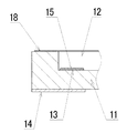
即ち、図1の工程(a)おいて、容器11はセラミック等の絶縁材で形成された表面実装に対応した形状であり、その一方の主面には凹部12が形成されている。この凹部12内の底面には、パッケージの長さ方向の一方端側の凹部内側壁面際に2つの素子接続用電極パッド13が形成されており、この素子接続用電極パッド13は容器11の他方の主面に形成した、他の基板等に固着導通するための外部接続用電極パッド14と各々電気的に接続されている。
That is, in the step (a) of FIG. 1, the
又、この容器11に形成した凹部12の形状は、凹部12の長さ及び幅の方向で凹部12内部に搭載する圧電振動板素子の長さ及び幅の方向に略相似した形状であり、凹部12の長さ及び幅方向の寸法は、圧電振動板素子を凹部12の中に挿入した際に、凹部12の内側壁面全てが圧電振動板素子に接触せず且つ圧電振動板素子の振動特性に悪影響を与えない最小の間隔が保てる寸法で形成されたものである。
The shape of the
更に、容器11において、凹部側壁頂部にはメタライズ層18が形成されており、これらが形成されている容器11を洗浄後所定の製造作業位置に配置する。
Further, in the
次の工程(b)及び(c)では、容器11凹部内底面に形成された素子接続用電極パッド13上に、容器11外より、ジェットディスペンス方式のディスペンサ19を用い、熱硬化性導電性インク15を吐出し、素子接続用電極パッド13表面に付着させる。熱硬化性導電性インク15は従来のエポキシ系導電性接着剤のようなペースト状ではなく、粘性の低い(5〜50mPa・s)液状であるためディスペンサの先端部を可能な限り細くすることができる。更に容器11の外部より素子接続用電極パッド13表面に吐出できるため、素子接続用電極パッド13が容器11の凹部内装壁面際に形成されていても、ディスペンサの形状や大きさに関係なく塗布できる。尚、熱硬化性導電性インク15は素子接続用電極パッド13の表面に付着後、素子接続用電極パッド表面上に薄く拡がる。
In the next steps (b) and (c), a thermosetting conductive ink is used from the outside of the
次に工程(d)では、付着した熱硬化性導電性インク15の上に圧電振動板素子16を、外部接続用電極膜17と熱硬化性導電性インク15とが接触且つ電気的に接続するように配置する。この圧電振動板素子16は、矩形状の圧電素板の表裏両主面上の表裏対向する位置に、金及びクロムによる多層構造の励振電極膜が形成されており、この表裏主面上に形成した励振電極膜からは圧電素板の長さ方向の一方の端部に向かって引出電極膜が延設されており、その先端には容器11の凹部12内に形成した素子接続用電極パッド13と固着導通する外部接続電極膜17が形成されて圧電振動板素子16を構成している。
Next, in the step (d), the
この圧電振動板素子16をコレットなどの保持具(図示せず)で保持しながら、圧電振動板素子16に形成した外部接続電極膜17が、所定の位置に配置した容器11の凹部12内に形成されている熱硬化性導電性インク15に対向し、且つ凹部12内の側壁面に圧電振動板素子16が接触しない位置に圧電振動板素子16を移動させ、所望の位置に圧電振動板素子16が配置されたら、保持具ごと圧電振動板素子16を凹部底面と水平に降下させ凹部22内に挿入し、外部接続電極膜17が熱硬化性導電性インク15と接触した位置で保持具を取り外す。
While holding the
次に、凹部12内に圧電振動板素子16を配置した容器をオーブン層などの加熱装置内に挿入し容器11全体を加熱し、熱硬化性導電性インク15を焼成し、圧電振動板素子16を素子接続用電極パッド13に固着する。
Next, the container in which the
その後、その凹部12の開口部を覆う金属製の蓋(図示せず)を容器12の側壁頂部のメタライズ層14の上に配置する。このとき、本発明では凹部12内に圧電振動板素子16を搭載する手段として、従来のようにエポキシ系導電性接着剤等が塗布されていないため、圧電振動板素子16搭載する凹部12の高さを可能な限り低い容器を使用することにより、圧電振動子としての薄型化を図れる。その後で、凹部11内の雰囲気を窒素に置換又は真空に抜気した後、気密封止することにより水晶振動子を形成する。
Thereafter, a metal lid (not shown) covering the opening of the
尚、本実施例で開示した圧電振動板素子を構成する圧電材料としては、水晶、セラミックス又はタンタル酸リチウム等の圧電材料に用いる。又、上記実施例で使用する熱硬化性導電性インクとしては、導電素材として金又は銀の粒子(粒径約数nm)を含有し、体積抵抗率は約3×10⁻⁶Ω・cmである。更に、金粒子の導電性インクでは三百数十℃で、銀粒子の導電性インクでは二百数十℃で20〜30分で焼成する性質を有するもの使用している。又、上記実施例では一つの容器のみで製造工程を説明したが、容器を複数個連結したシート状の容器群とし、一度に複数個の圧電振動子を製造できる工法を用いる場合でも、本発明に開示の技術はその効果を奏することができる。 In addition, as a piezoelectric material which comprises the piezoelectric diaphragm element disclosed by the present Example, it uses for piezoelectric materials, such as a crystal | crystallization, ceramics, or lithium tantalate. In addition, the thermosetting conductive ink used in the above examples contains gold or silver particles (particle diameter of about several nm) as a conductive material, and the volume resistivity is about 3 × 10 −6 Ω · cm. is there. Further, the conductive ink of gold particles is used at a temperature of 300 to tens of degrees Celsius, and the conductive ink of silver particles is used at a temperature of 200 to tens of degrees Celsius and baked in 20 to 30 minutes. In the above embodiment, the manufacturing process has been described with only one container. However, the present invention can be applied to the case where a sheet-like container group in which a plurality of containers are connected and a method of manufacturing a plurality of piezoelectric vibrators at a time is used. The technique disclosed in (1) can achieve the effect.
11,容器
12,凹部
13,素子接続用電極パッド
15,熱硬化性導電性インク
16,圧電振動板素子
17,外部接続電極膜
19,ジェットディスペンス方式ディスペンサ
11,
Claims (1)
該凹部内底面に形成された該素子接続用電極パッド上に、該容器外より、ジェットディスペンス方式のディスペンサを用い、熱硬化性導電性インクを吐出し、該素子接続用電極パッド表面に付着させる工程と、
付着した該熱硬化性導電性インクの上に該圧電振動板素子を、該外部接続用電極膜と該熱硬化性導電性インクとが接触且つ電気的に接続するように配置する工程と、
該凹部内に該圧電振動板素子を配置した該容器を加熱し、該熱硬化性導電性インクを焼成し該圧電振動板素子を該素子接続用電極パッドに固着する工程と
を具備することを特徴とする圧電振動子の製造方法。 A container formed of an insulating material is provided with a recess, and an electrode pad for element connection is formed at the end in the length direction of the bottom of the recess, and an excitation electrode film is formed on both the front and back main surfaces in the recess. And a piezoelectric diaphragm element in which an external connection electrode film electrically connected to the excitation electrode film is formed at the end in the length direction, and the external connection electrode film of the piezoelectric diaphragm and the element connection electrode In a method of manufacturing a piezoelectric vibrator in which a pad is electrically connected and fixed with a conductive material,
On the element connection electrode pad formed on the inner bottom surface of the concave portion, the thermosetting conductive ink is ejected from the outside of the container by using a jet dispensing type dispenser and adhered to the surface of the element connection electrode pad. Process,
Arranging the piezoelectric diaphragm element on the adhered thermosetting conductive ink so that the electrode film for external connection and the thermosetting conductive ink are in contact and electrically connected;
Heating the container in which the piezoelectric diaphragm element is disposed in the recess, firing the thermosetting conductive ink, and fixing the piezoelectric diaphragm element to the element connection electrode pad. A method for manufacturing a piezoelectric vibrator.
Priority Applications (1)
| Application Number | Priority Date | Filing Date | Title |
|---|---|---|---|
| JP2004104725A JP2005295041A (en) | 2004-03-31 | 2004-03-31 | Method for manufacturing piezoelectric vibrator |
Applications Claiming Priority (1)
| Application Number | Priority Date | Filing Date | Title |
|---|---|---|---|
| JP2004104725A JP2005295041A (en) | 2004-03-31 | 2004-03-31 | Method for manufacturing piezoelectric vibrator |
Publications (1)
| Publication Number | Publication Date |
|---|---|
| JP2005295041A true JP2005295041A (en) | 2005-10-20 |
Family
ID=35327520
Family Applications (1)
| Application Number | Title | Priority Date | Filing Date |
|---|---|---|---|
| JP2004104725A Pending JP2005295041A (en) | 2004-03-31 | 2004-03-31 | Method for manufacturing piezoelectric vibrator |
Country Status (1)
| Country | Link |
|---|---|
| JP (1) | JP2005295041A (en) |
Cited By (6)
| Publication number | Priority date | Publication date | Assignee | Title |
|---|---|---|---|---|
| JP2007135191A (en) * | 2005-10-12 | 2007-05-31 | Epson Toyocom Corp | Piezoelectric device and manufacturing method thereof |
| JP2007235340A (en) * | 2006-02-28 | 2007-09-13 | Kyocera Kinseki Corp | Piezoelectric device and method for manufacturing piezoelectric device |
| WO2007106318A3 (en) * | 2006-03-03 | 2007-12-21 | Second Sight Medical Prod Inc | Biocompatible bonding method and electronics package suitable for implantation |
| JP2009182873A (en) * | 2008-01-31 | 2009-08-13 | Daishinku Corp | Method for manufacturing piezoelectric vibration device and piezoelectric vibration device |
| WO2016136015A1 (en) * | 2015-02-24 | 2016-09-01 | 株式会社村田製作所 | Piezoelectric vibration component and application method |
| JP2017212508A (en) * | 2016-05-24 | 2017-11-30 | 日本電波工業株式会社 | Piezoelectric device and manufacturing method thereof |
-
2004
- 2004-03-31 JP JP2004104725A patent/JP2005295041A/en active Pending
Cited By (9)
| Publication number | Priority date | Publication date | Assignee | Title |
|---|---|---|---|---|
| US7645262B2 (en) | 2002-04-11 | 2010-01-12 | Second Sight Medical Products, Inc. | Biocompatible bonding method and electronics package suitable for implantation |
| JP2007135191A (en) * | 2005-10-12 | 2007-05-31 | Epson Toyocom Corp | Piezoelectric device and manufacturing method thereof |
| JP2007235340A (en) * | 2006-02-28 | 2007-09-13 | Kyocera Kinseki Corp | Piezoelectric device and method for manufacturing piezoelectric device |
| WO2007106318A3 (en) * | 2006-03-03 | 2007-12-21 | Second Sight Medical Prod Inc | Biocompatible bonding method and electronics package suitable for implantation |
| JP2009182873A (en) * | 2008-01-31 | 2009-08-13 | Daishinku Corp | Method for manufacturing piezoelectric vibration device and piezoelectric vibration device |
| WO2016136015A1 (en) * | 2015-02-24 | 2016-09-01 | 株式会社村田製作所 | Piezoelectric vibration component and application method |
| JPWO2016136015A1 (en) * | 2015-02-24 | 2018-01-25 | 株式会社村田製作所 | Piezoelectric vibration component and coating method |
| US10749102B2 (en) | 2015-02-24 | 2020-08-18 | Murata Manufacturing Co., Ltd. | Piezoelectric vibration component and application method |
| JP2017212508A (en) * | 2016-05-24 | 2017-11-30 | 日本電波工業株式会社 | Piezoelectric device and manufacturing method thereof |
Similar Documents
| Publication | Publication Date | Title |
|---|---|---|
| CN102377401B (en) | The manufacture method of electronic device, electronic equipment and electronic device | |
| KR101487780B1 (en) | Electronic device | |
| US7583162B2 (en) | Piezoelectric device and method for manufacturing the piezoelectric device | |
| JP2005295041A (en) | Method for manufacturing piezoelectric vibrator | |
| JP2007013444A (en) | Piezoelectric vibration device and manufacturing method thereof | |
| JP5123041B2 (en) | Method for manufacturing piezoelectric device | |
| JP2005217810A (en) | Method for manufacturing piezoelectric vibrator | |
| JP5734099B2 (en) | Electronic equipment | |
| JP2021010152A (en) | Crystal device | |
| JP4443306B2 (en) | Manufacturing method of crystal unit | |
| JP2010157813A (en) | Method for manufacturing piezoelectric device | |
| JP2962924B2 (en) | Electronic component storage package | |
| JPH05275552A (en) | Package for encapsulating electronic component | |
| JP2016103753A (en) | Crystal device | |
| JP2012244003A (en) | Electronic apparatus | |
| JP2017183856A (en) | Crystal oscillator | |
| JPH05299963A (en) | Electronic component storage container | |
| JP2005260525A (en) | Package for surface mounted piezoelectric device and manufacturing method of surface mounted piezoelectric device | |
| JP2005217809A (en) | Piezoelectric vibrator and manufacturing method thereof | |
| JPH05167378A (en) | Electronic component storage package | |
| JP2017183966A (en) | Crystal oscillator | |
| JP2012156313A (en) | Electronic apparatus | |
| JP2020120264A (en) | Crystal device and electronic apparatus | |
| JPH0637194A (en) | Package for storing electronic components | |
| JP2003218260A (en) | Package for accommodating electronic component |
Legal Events
| Date | Code | Title | Description |
|---|---|---|---|
| A621 | Written request for application examination |
Free format text: JAPANESE INTERMEDIATE CODE: A621 Effective date: 20070329 |
|
| A131 | Notification of reasons for refusal |
Effective date: 20090909 Free format text: JAPANESE INTERMEDIATE CODE: A131 |
|
| A02 | Decision of refusal |
Free format text: JAPANESE INTERMEDIATE CODE: A02 Effective date: 20091208 |