JP2005295032A - Method of manufacturing surface acoustic wave element - Google Patents
Method of manufacturing surface acoustic wave element Download PDFInfo
- Publication number
- JP2005295032A JP2005295032A JP2004104568A JP2004104568A JP2005295032A JP 2005295032 A JP2005295032 A JP 2005295032A JP 2004104568 A JP2004104568 A JP 2004104568A JP 2004104568 A JP2004104568 A JP 2004104568A JP 2005295032 A JP2005295032 A JP 2005295032A
- Authority
- JP
- Japan
- Prior art keywords
- substrate
- acoustic wave
- surface acoustic
- resist film
- manufacturing
- Prior art date
- Legal status (The legal status is an assumption and is not a legal conclusion. Google has not performed a legal analysis and makes no representation as to the accuracy of the status listed.)
- Granted
Links
- 238000010897 surface acoustic wave method Methods 0.000 title claims abstract description 45
- 238000004519 manufacturing process Methods 0.000 title claims abstract description 35
- 239000000758 substrate Substances 0.000 claims abstract description 98
- 238000005498 polishing Methods 0.000 claims abstract description 8
- 238000000034 method Methods 0.000 claims description 20
- 229910052751 metal Inorganic materials 0.000 claims description 13
- 239000002184 metal Substances 0.000 claims description 13
- WSMQKESQZFQMFW-UHFFFAOYSA-N 5-methyl-pyrazole-3-carboxylic acid Chemical compound CC1=CC(C(O)=O)=NN1 WSMQKESQZFQMFW-UHFFFAOYSA-N 0.000 claims description 4
- GQYHUHYESMUTHG-UHFFFAOYSA-N lithium niobate Chemical compound [Li+].[O-][Nb](=O)=O GQYHUHYESMUTHG-UHFFFAOYSA-N 0.000 claims description 4
- 238000000151 deposition Methods 0.000 claims 1
- 238000012545 processing Methods 0.000 abstract description 2
- 230000003667 anti-reflective effect Effects 0.000 abstract 2
- 230000008021 deposition Effects 0.000 abstract 1
- 238000002310 reflectometry Methods 0.000 description 15
- 229920002120 photoresistant polymer Polymers 0.000 description 5
- 239000010410 layer Substances 0.000 description 4
- 230000008569 process Effects 0.000 description 4
- 230000015572 biosynthetic process Effects 0.000 description 3
- 239000000463 material Substances 0.000 description 3
- 230000008859 change Effects 0.000 description 2
- 238000011161 development Methods 0.000 description 2
- PCHJSUWPFVWCPO-UHFFFAOYSA-N gold Chemical compound [Au] PCHJSUWPFVWCPO-UHFFFAOYSA-N 0.000 description 2
- 239000010931 gold Substances 0.000 description 2
- 229910052737 gold Inorganic materials 0.000 description 2
- 230000009467 reduction Effects 0.000 description 2
- ATJFFYVFTNAWJD-UHFFFAOYSA-N Tin Chemical compound [Sn] ATJFFYVFTNAWJD-UHFFFAOYSA-N 0.000 description 1
- 230000008901 benefit Effects 0.000 description 1
- 238000007796 conventional method Methods 0.000 description 1
- 238000010586 diagram Methods 0.000 description 1
- 230000000694 effects Effects 0.000 description 1
- 239000007772 electrode material Substances 0.000 description 1
- 238000005516 engineering process Methods 0.000 description 1
- 238000005530 etching Methods 0.000 description 1
- 239000012535 impurity Substances 0.000 description 1
- 238000005259 measurement Methods 0.000 description 1
- 238000012986 modification Methods 0.000 description 1
- 230000004048 modification Effects 0.000 description 1
- 238000007747 plating Methods 0.000 description 1
- 238000007788 roughening Methods 0.000 description 1
- 239000002356 single layer Substances 0.000 description 1
- 230000001629 suppression Effects 0.000 description 1
Images
Landscapes
- Photosensitive Polymer And Photoresist Processing (AREA)
- Materials For Photolithography (AREA)
- Surface Acoustic Wave Elements And Circuit Networks Thereof (AREA)
Abstract
Description
本発明は、電極パターンをリフトオフによって形成する弾性表面波素子の製造方法に関するものである。 The present invention relates to a method for manufacturing a surface acoustic wave device in which an electrode pattern is formed by lift-off.
従来、この技術の分野における弾性表面波素子の製造方法は、例えば、下記特許文献1に開示されている。この公報に記載の弾性表面波素子の製造方法においては、まず、圧電基板上に、反射防止膜及びフォトレジスト膜を順次積層した後、基板を所定形状のパターンが描かれたフォトマスクを介して紫外光(例えば、i線やg線等)で露光する。次に、現像処理によって、所定形状のレジストパターンを形成し、その後、基板全面に電極膜を蒸着する。そして、フォトレジスト膜上に積層した部分の電極膜をリフトオフによって除去することで、圧電基板上に所定形状の電極パターンが形成された弾性表面波素子の作製が完了する。
Conventionally, a method for manufacturing a surface acoustic wave element in the field of this technology is disclosed in, for example,
ここで、基板上に積層される反射防止膜は、露光時に照射される紫外光が圧電基板の裏面で反射するのを防止するためのものである。そして、この反射防止膜の採用により、フォトレジスト膜の意図しない部分への露光が防止されており、それにより電極パターンの寸法精度の向上が図られている。 Here, the antireflection film laminated on the substrate is for preventing the ultraviolet light irradiated during exposure from being reflected on the back surface of the piezoelectric substrate. By adopting this antireflection film, exposure to an unintended portion of the photoresist film is prevented, thereby improving the dimensional accuracy of the electrode pattern.
しかしながら、前述した従来の弾性表面波素子の製造方法には、次のような課題が存在している。すなわち、たとえ反射防止膜によって電極パターンの寸法精度の向上を図っても、ウエハ面内でこの反射防止膜の厚さが不均一である場合には、フォトレジスト膜の厚さにもばらつきが生じるため、電極パターンを所望の寸法に成形することができない。それにより、電極パターンの寸法精度が著しく低下し、弾性表面波素子の中心周波数の誤差が拡大する結果を招いてしまう。 However, the conventional method for manufacturing a surface acoustic wave device described above has the following problems. That is, even if the dimensional accuracy of the electrode pattern is improved by the antireflection film, if the thickness of the antireflection film is not uniform within the wafer surface, the thickness of the photoresist film also varies. Therefore, the electrode pattern cannot be formed to a desired dimension. As a result, the dimensional accuracy of the electrode pattern is remarkably lowered, and the error of the center frequency of the surface acoustic wave element is increased.
従って、反射防止膜はできる限り均一な厚さにすることが好ましいが、反射防止膜の成膜に一般的に利用されるスピンコート法で均一な厚さの反射防止膜を成膜することは非常に困難な上、その成膜処理には多大な手間と時間を要するという問題があった。 Therefore, it is preferable that the antireflection film has a uniform thickness as much as possible. However, it is not possible to form an antireflection film with a uniform thickness by a spin coat method generally used for forming an antireflection film. In addition to being very difficult, the film forming process has a problem of requiring a lot of labor and time.
そこで、本発明は、上述の課題を解決するためになされたもので、寸法精度の高い電極パターンを容易に作製することができる弾性表面波素子の製造方法を提供することを目的とする。 Accordingly, the present invention has been made to solve the above-described problems, and an object of the present invention is to provide a method of manufacturing a surface acoustic wave device that can easily produce an electrode pattern with high dimensional accuracy.
本発明に係る弾性表面波素子の製造方法は、鏡面研磨時におけるi線の反射率が10%以下である圧電基板の表面に、レジスト膜を成膜するステップと、レジスト膜の上方に、所望の電極パターンに対応するパターンが描かれたフォトマスクを配置し、フォトマスクを介してレジスト膜を露光するステップと、露光されたレジスト膜を現像するステップと、レジスト膜が現像された圧電基板の表面に、金属膜を成膜するステップと、レジスト膜上に成膜された部分の金属膜をリフトオフ除去して、金属膜を所望の電極パターンに成形するステップとを有することを特徴とする。 The method for manufacturing a surface acoustic wave device according to the present invention includes a step of forming a resist film on a surface of a piezoelectric substrate having a reflectance of 10% or less during mirror polishing, and a desired position above the resist film. A photomask on which a pattern corresponding to the electrode pattern is placed, exposing the resist film through the photomask, developing the exposed resist film, and the piezoelectric substrate on which the resist film is developed The method includes a step of forming a metal film on the surface and a step of lift-off removing a portion of the metal film formed on the resist film to form a metal film into a desired electrode pattern.
この弾性表面波素子の製造方法においては、鏡面研磨時におけるi線の反射率が10%以下である圧電基板を用いることで、露光時に照射されるi線等の紫外光の大部分が基板に吸収される。それにより、露光時に照射される光の基板裏面における反射が有意に抑制されるため、基板によって露光される側の基板面に反射防止膜を成膜することなく、高い寸法精度を有する電極パターンを形成することができる。すなわち、この弾性表面波素子の製造方法によれば、多大な手間と時間を要する反射防止膜の成膜処理が必要な従来の製造方法に比べて、寸法精度の高い電極パターンを容易に作製することができる。 In this surface acoustic wave device manufacturing method, a piezoelectric substrate having an i-line reflectivity of 10% or less during mirror polishing is used, so that most of ultraviolet light such as i-rays irradiated during exposure is applied to the substrate. Absorbed. As a result, the reflection of light irradiated at the time of exposure on the back surface of the substrate is significantly suppressed, so that an electrode pattern having high dimensional accuracy can be formed without forming an antireflection film on the substrate surface on the side exposed by the substrate. Can be formed. That is, according to this method of manufacturing a surface acoustic wave element, an electrode pattern with high dimensional accuracy can be easily manufactured as compared with a conventional manufacturing method that requires a film formation process of an antireflection film that requires a lot of labor and time. be able to.
本発明に係る弾性表面波素子の製造方法は、鏡面研磨時におけるg線の反射率が10%以下である圧電基板の表面に、レジスト膜を成膜するステップと、レジスト膜の上方に、所望の電極パターンに対応するパターンが描かれたフォトマスクを配置し、フォトマスクを介してレジスト膜を露光するステップと、露光されたレジスト膜を現像するステップと、レジスト膜が現像された圧電基板の表面に、金属膜を成膜するステップと、レジスト膜上に成膜された部分の金属膜をリフトオフ除去して、金属膜を所望の電極パターンに成形するステップとを有することを特徴とする。 The method of manufacturing a surface acoustic wave device according to the present invention includes a step of forming a resist film on the surface of a piezoelectric substrate having a g-line reflectance of 10% or less during mirror polishing, and a desired position above the resist film. A photomask on which a pattern corresponding to the electrode pattern is placed, exposing the resist film through the photomask, developing the exposed resist film, and the piezoelectric substrate on which the resist film is developed The method includes a step of forming a metal film on the surface and a step of lift-off removing a portion of the metal film formed on the resist film to form a metal film into a desired electrode pattern.
この弾性表面波素子の製造方法においては、鏡面研磨時におけるg線の反射率が10%以下である圧電基板を用いることで、露光時に照射されるg線等の紫外光の大部分が基板に吸収される。それにより、露光時に照射される光の基板裏面における反射が有意に抑制されるため、基板によって露光される側の基板面に反射防止膜を成膜することなく、高い寸法精度を有する電極パターンを形成することができる。すなわち、この弾性表面波素子の製造方法によれば、多大な手間と時間を要する反射防止膜の成膜処理が必要な従来の製造方法に比べて、寸法精度の高い電極パターンを容易に作製することができる。 In this surface acoustic wave device manufacturing method, a piezoelectric substrate having a g-line reflectance of 10% or less during mirror polishing is used, so that most of ultraviolet light such as g-rays irradiated during exposure is applied to the substrate. Absorbed. As a result, the reflection of light irradiated at the time of exposure on the back surface of the substrate is significantly suppressed, so that an electrode pattern having high dimensional accuracy can be formed without forming an antireflection film on the substrate surface on the side exposed by the substrate. Can be formed. That is, according to this method of manufacturing a surface acoustic wave element, an electrode pattern with high dimensional accuracy can be easily manufactured as compared with a conventional manufacturing method that requires a film formation process of an antireflection film that requires a lot of labor and time. be able to.
また、レジスト膜を露光する際にi線又はg線を用いることが好ましい。 Further, it is preferable to use i-line or g-line when exposing the resist film.
圧電基板が、Mn又はFeがドープされたタンタル酸リチウム基板(LT基板)、又はMn又はFeがドープされたニオブ酸リチウム基板(LN基板)であることが好ましい。発明者らは、LT基板又はLN基板に、Mn又はFeをドープすることにより、鏡面研磨時におけるi線又はg線の反射率が10%以下である上記圧電基板が得られることを見出した。 The piezoelectric substrate is preferably a lithium tantalate substrate (LT substrate) doped with Mn or Fe, or a lithium niobate substrate (LN substrate) doped with Mn or Fe. The inventors have found that the above-described piezoelectric substrate having an i-line or g-line reflectance of 10% or less during mirror polishing can be obtained by doping the LT substrate or LN substrate with Mn or Fe.
本発明によれば、寸法精度の高い電極パターンを容易に作製することができる弾性表面波素子の製造方法が提供される。 ADVANTAGE OF THE INVENTION According to this invention, the manufacturing method of the surface acoustic wave element which can produce an electrode pattern with high dimensional accuracy easily is provided.
以下、添付図面を参照して本発明に係る弾性表面波素子の製造方法を実施するにあたり最良と思われる形態について詳細に説明する。なお、同一又は同等の要素については同一の符号を付し、説明が重複する場合にはその説明を省略する。 DETAILED DESCRIPTION OF THE PREFERRED EMBODIMENTS Embodiments that are considered to be the best for carrying out a surface acoustic wave device manufacturing method according to the present invention will be described below in detail with reference to the accompanying drawings. In addition, the same code | symbol is attached | subjected about the same or equivalent element, and the description is abbreviate | omitted when description overlaps.
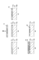
まず、図1を参照しつつ、弾性表面波素子を作製する手順について説明する。 First, a procedure for producing a surface acoustic wave element will be described with reference to FIG.
弾性表面波素子の作製にあたり、表面10aが鏡面研磨(Ra0.2nm)されたLT基板10を準備する。このLT基板10は、所定量のFeがドープされたLT基板(タンタル酸リチウム基板)であり、後述するように、ノンドープのLT基板に比べてi線(波長365nmの紫外線)の反射率が低くなっている。なお、LT基板10の裏面10bは、作製される弾性表面波素子においてバルク波が生じないように、粗面化処理が施されている。
In producing the surface acoustic wave element, an
そして、このLT基板10の表面10aに、ペースト状のレジストを塗布して、所定のレジスト膜12を成膜する(図1(a)参照)。このレジスト膜12には、公知のポジ型レジスト膜を利用することができる。なお、図1では、ポジ型のレジスト膜を示しているが、必要に応じてネガ型のレジスト膜を利用することができる。
Then, a paste-like resist is applied to the
次に、所望のIDT電極のパターンや入出力電極のパターンがパターニングされたフォトマスク14をレジスト膜12の上方に配置し、このフォトマスク14を介してレジスト膜12を露光する(図1(b)参照)。この露光の際に用いる紫外線は、波長が365nmであるi線である。つまり、LT基板10は、上述したようにi線の反射率が低いものであるため、レジスト膜12を通過したi線は、基板内に進入すると共に基板内部においてその大部分が吸収される。なお、露光に用いる紫外線は、波長が436nmであるg線を用いてもよい。
Next, a
そして、図示しない現像液を用いてレジスト膜12を現像し、フォトマスク14のパターンと同パターンのレジストパターン16を得る(図1(c)参照)。その後、現像によってレジストパターン16が形成された基板表面10aに、Al電極膜(金属膜)18を成膜する(図1(d)参照)。最後に、図示しないエッチング液を用いてレジストパターン16上に成膜された部分のAl電極膜18をリフトオフによって除去して、電極パターン20を得ることにより、弾性表面波素子22の作製が完了する(図1(e)参照)。
Then, the
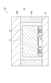
この弾性表面波素子22は、図2に示したような弾性表面波装置24に適用される。つまり、弾性表面波素子22は、入出力電極26上に嵩上げ電極28が形成された後、弾性表面波素子22の動作に必要な電圧を印加するための金メッキ電極30が形成された実装基板32上にフリップチップ実装される。なお、対応する弾性表面波素子22の嵩上げ電極28と実装基板32の金メッキ電極30とは、金バンプ34を介して接続されている。符号36は、弾性表面波素子22を密封封止して保護するカバーであり、弾性表面波素子の側面を四方から囲むダム部36Aと弾性表面波素子の上面を覆うキャップ部36Bの2つの部材で構成されている。
The surface acoustic wave element 22 is applied to a surface
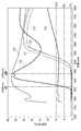
次に、LT基板10へのドーピング(不純物添加)と、レジスト膜12の露光に用いるi線との関係について、図3を参照しつつ説明する。ここで図3は、露光される光の波長に対する基板の反射率の変化を示したグラフであり、横軸は波長(nm)を、縦軸は反射率(%)を示している。なお、反射率の測定には、日立製作所のU−3400吸光度計装置(積分球付き)を用いた。
Next, the relationship between doping (impurity addition) to the
図3のグラフにおいて、曲線C0はノンドープLT基板を示しており、また、曲線C1、曲線C2及び曲線C3はそれぞれ、Feを0.21wt%、0.31wt%及び0.58wt%添加したLT基板を示している。なお、各基板の反射率はRa0.2nm程度に鏡面研磨した状態で測定した。 In the graph of FIG. 3, a curve C0 indicates a non-doped LT substrate, and a curve C1, a curve C2, and a curve C3 are LT substrates to which Fe is added at 0.21 wt%, 0.31 wt%, and 0.58 wt%, respectively. Is shown. In addition, the reflectance of each substrate was measured in a state of being mirror-polished to about Ra 0.2 nm.
このグラフから明らかなように、波長365nmのi線付近においては、FeがドープされたLT基板(曲線C1〜C3)の反射率は、ノンドープLT基板(曲線C0)の反射率よりも低くなっている。より具体的には、ノンドープLT基板C0のi線反射率は36%程度であるが、FeがドープされたLT基板C1〜C3のi線反射率は10%以下(約0.5%)となっている。 As is apparent from this graph, the reflectance of the LT substrate doped with Fe (curves C1 to C3) is lower than that of the non-doped LT substrate (curve C0) in the vicinity of the i-line having a wavelength of 365 nm. Yes. More specifically, the i-line reflectivity of the non-doped LT substrate C0 is about 36%, but the i-line reflectivity of the Fe-doped LT substrates C1 to C3 is 10% or less (about 0.5%). It has become.
このように、Feのドープによってi線反射率が10%以下まで低減されたLT基板10を弾性表面波素子22の作製に用いた場合には、露光時に照射されるi線をほとんど反射しない。そのため、成膜に多大な手間と時間を要する反射防止膜を用いることなく、高い寸法精度を有する電極パターン20を作製することができる。すなわち、上述した弾性表面波素子の製造方法によれば、反射防止膜を用いる従来の製造方法に比べて、高い寸法精度を有する電極パターンを容易に作製することができる。
As described above, when the
また、基板表面に反射防止膜を成膜する従来の製造方法では、基板材料と反射防止膜材料との屈折率の相違により、基板表面においても露光時に照射される紫外線の反射がおこってしまう。つまり、基板と反射防止膜との界面において反射された光によって、意図しない部分への露光がおこなわれ、レジスト膜の寸法精度が低下することがあった。一方、上述した製造方法によれば、LT基板10が露光時に照射されるi線を吸収することによって基板裏面10bにおける反射が抑制される上、反射防止膜の省略によって基板表面10aにおける反射も抑制される。このような反射の抑制は、線幅が1μm以下の微細な電極パターンを作製する際に特に有効である。
Further, in the conventional manufacturing method in which an antireflection film is formed on the substrate surface, the difference in refractive index between the substrate material and the antireflection film material results in reflection of ultraviolet rays irradiated during exposure on the substrate surface. That is, the light reflected at the interface between the substrate and the antireflection film may expose an unintended portion, resulting in a decrease in the dimensional accuracy of the resist film. On the other hand, according to the manufacturing method described above, the
図3において、曲線C4はMnを0.32wt%添加したLT基板を示しており、曲線C5は基板表面に還元処理を施したノンドープLT基板を示している。これらの基板の反射率も、Ra0.2nm程度に鏡面研磨した状態で測定した。そして、曲線C4から明らかなように、MnのドープによってもLT基板のi線反射率を10%以下(約6%)まで低下させることができる。また、曲線C5から、基板表面に還元処理を施したLT基板であっても、i線反射率を10%以下(約9%)まで低下させることができることがわかる。 In FIG. 3, a curve C4 indicates an LT substrate to which 0.32 wt% of Mn is added, and a curve C5 indicates a non-doped LT substrate in which the substrate surface is subjected to reduction treatment. The reflectances of these substrates were also measured in a state of being mirror polished to about Ra 0.2 nm. As is apparent from the curve C4, the i-line reflectivity of the LT substrate can be lowered to 10% or less (about 6%) even by doping with Mn. Further, it can be seen from the curve C5 that the i-line reflectivity can be reduced to 10% or less (about 9%) even with the LT substrate in which the substrate surface is subjected to the reduction treatment.
なお、本実施形態に用いるLT基板は、i線反射率が5%以下であるLT基板がより好ましく、さらにはi線反射率が1%以下であるLT基板がより好ましい。基板のi線反射率を低減するために、適宜、FeやMn以外の材料をLT基板にドープしてもよい。 The LT substrate used in this embodiment is more preferably an LT substrate having an i-line reflectivity of 5% or less, and more preferably an LT substrate having an i-line reflectivity of 1% or less. In order to reduce the i-line reflectivity of the substrate, materials other than Fe and Mn may be appropriately doped into the LT substrate.
また、i線反射率が10%以下のLT基板ではなく、g線反射率が10%以下のLT基板であっても、上述したLT基板10と同一又は同等の効果を得ることができる。さらに、その場合においても、g線反射率が5%以下であるLT基板がより好ましく、さらにはg線反射率が1%以下であるLT基板がより好ましい。
Even if the LT substrate has an i-line reflectance of 10% or less and an LT substrate having a g-line reflectance of 10% or less, the same or equivalent effect as the
ここで、i線反射率やg線反射率は、i線やg線と完全に一致する波長によって測定された反射率に限らず、i線やg線と実質的に同等の波長によって測定された反射率をも含むものとする。 Here, the i-line reflectivity and the g-line reflectivity are not limited to reflectivities measured at wavelengths that completely match the i-line and g-line, but are measured at wavelengths substantially equivalent to the i-line and g-line. The reflectance is also included.
本発明は上記実施形態に限定されるものではなく、様々な変形が可能である。例えば、上記弾性表面波素子の製造方法に用いる圧電基板は、LT基板に限定されず、LN基板(ニオブ酸リチウム基板)であってもよい。また、電極膜は、Al電極膜に限らず、様々な電極材料に適宜変更することができる。さらに、電極膜は、単層構造に限らず、下層にバッファ層として機能する層(例えば、TiN層等)を含む多層構造であってもよい。また、レジスト膜の露光に用いる紫外線は、i線やg線に限らず、例えば、KrF光源やArF光源等を利用した光を用いることも可能である。 The present invention is not limited to the above embodiment, and various modifications are possible. For example, the piezoelectric substrate used in the method for manufacturing the surface acoustic wave element is not limited to the LT substrate, and may be an LN substrate (lithium niobate substrate). The electrode film is not limited to the Al electrode film, and can be appropriately changed to various electrode materials. Furthermore, the electrode film is not limited to a single layer structure, and may have a multilayer structure including a layer functioning as a buffer layer (for example, a TiN layer) in the lower layer. Moreover, the ultraviolet rays used for exposure of the resist film are not limited to i-line and g-line, and for example, light using a KrF light source, an ArF light source, or the like can be used.
10…LT基板、12…レジスト膜、14…フォトマスク、16…レジストパターン、18…Al電極膜、20…電極パターン、22…弾性表面波素子、24…弾性表面波装置。
DESCRIPTION OF
Claims (8)
前記レジスト膜の上方に、所望の電極パターンに対応するパターンが描かれたフォトマスクを配置し、前記フォトマスクを介して前記レジスト膜を露光するステップと、
露光された前記レジスト膜を現像するステップと、
前記レジスト膜が現像された前記圧電基板の表面に、金属膜を成膜するステップと、
前記レジスト膜上に成膜された部分の前記金属膜をリフトオフ除去して、前記金属膜を前記所望の電極パターンに成形するステップと
を有する、弾性表面波素子の製造方法。 Depositing a resist film on the surface of a piezoelectric substrate having a reflectance of 10% or less at the time of mirror polishing;
Placing a photomask on which a pattern corresponding to a desired electrode pattern is drawn above the resist film, and exposing the resist film through the photomask;
Developing the exposed resist film;
Forming a metal film on the surface of the piezoelectric substrate on which the resist film has been developed;
And a step of lift-off removing the portion of the metal film formed on the resist film to form the metal film into the desired electrode pattern.
前記レジスト膜の上方に、所望の電極パターンに対応するパターンが描かれたフォトマスクを配置し、前記フォトマスクを介して前記レジスト膜を露光するステップと、
露光された前記レジスト膜を現像するステップと、
前記レジスト膜が現像された前記圧電基板の表面に、金属膜を成膜するステップと、
前記レジスト膜上に成膜された部分の前記金属膜をリフトオフ除去して、前記金属膜を前記所望の電極パターンに成形するステップと
を有する、弾性表面波素子の製造方法。 Forming a resist film on the surface of the piezoelectric substrate having a g-line reflectance of 10% or less during mirror polishing;
Placing a photomask on which a pattern corresponding to a desired electrode pattern is drawn above the resist film, and exposing the resist film through the photomask;
Developing the exposed resist film;
Forming a metal film on the surface of the piezoelectric substrate on which the resist film has been developed;
And a step of lift-off removing the portion of the metal film formed on the resist film to form the metal film into the desired electrode pattern.
Priority Applications (1)
| Application Number | Priority Date | Filing Date | Title |
|---|---|---|---|
| JP2004104568A JP3999757B2 (en) | 2004-03-31 | 2004-03-31 | Manufacturing method of surface acoustic wave device |
Applications Claiming Priority (1)
| Application Number | Priority Date | Filing Date | Title |
|---|---|---|---|
| JP2004104568A JP3999757B2 (en) | 2004-03-31 | 2004-03-31 | Manufacturing method of surface acoustic wave device |
Publications (2)
| Publication Number | Publication Date |
|---|---|
| JP2005295032A true JP2005295032A (en) | 2005-10-20 |
| JP3999757B2 JP3999757B2 (en) | 2007-10-31 |
Family
ID=35327515
Family Applications (1)
| Application Number | Title | Priority Date | Filing Date |
|---|---|---|---|
| JP2004104568A Expired - Fee Related JP3999757B2 (en) | 2004-03-31 | 2004-03-31 | Manufacturing method of surface acoustic wave device |
Country Status (1)
| Country | Link |
|---|---|
| JP (1) | JP3999757B2 (en) |
Cited By (3)
| Publication number | Priority date | Publication date | Assignee | Title |
|---|---|---|---|---|
| JP2010171392A (en) * | 2008-12-25 | 2010-08-05 | Ngk Insulators Ltd | Composite substrate and method for forming metal pattern |
| JP2010245991A (en) * | 2009-04-09 | 2010-10-28 | Shin-Etsu Chemical Co Ltd | Surface acoustic wave device substrate and manufacturing method thereof |
| WO2025215946A1 (en) * | 2024-04-12 | 2025-10-16 | 信越化学工業株式会社 | Oxide single crystal composite substrate and method for manufacturing same |
Families Citing this family (1)
| Publication number | Priority date | Publication date | Assignee | Title |
|---|---|---|---|---|
| US11394364B2 (en) | 2019-02-15 | 2022-07-19 | Skyworks Solutions, Inc. | Acoustic wave device with anti-reflection layer |
-
2004
- 2004-03-31 JP JP2004104568A patent/JP3999757B2/en not_active Expired - Fee Related
Cited By (3)
| Publication number | Priority date | Publication date | Assignee | Title |
|---|---|---|---|---|
| JP2010171392A (en) * | 2008-12-25 | 2010-08-05 | Ngk Insulators Ltd | Composite substrate and method for forming metal pattern |
| JP2010245991A (en) * | 2009-04-09 | 2010-10-28 | Shin-Etsu Chemical Co Ltd | Surface acoustic wave device substrate and manufacturing method thereof |
| WO2025215946A1 (en) * | 2024-04-12 | 2025-10-16 | 信越化学工業株式会社 | Oxide single crystal composite substrate and method for manufacturing same |
Also Published As
| Publication number | Publication date |
|---|---|
| JP3999757B2 (en) | 2007-10-31 |
Similar Documents
| Publication | Publication Date | Title |
|---|---|---|
| TW521318B (en) | Phase-shift masks and methods of fabrication | |
| KR102291647B1 (en) | Planarized extreme ultraviolet lithography blank with absorber and manufacturing system therefor | |
| EP2750164A1 (en) | Reflective mask and method for manufacturing same | |
| CN104820339A (en) | Mask structures and methods of manufacturing | |
| JP7106492B2 (en) | MASK BLANK, PHASE SHIFT MASK, AND SEMICONDUCTOR DEVICE MANUFACTURING METHOD | |
| KR20190126725A (en) | EUV lithography mask, and fabricating method of the same | |
| KR101679687B1 (en) | Reflective extreme ultraviolet mask and method of manufacturing the same | |
| JP2010225698A (en) | Pattern forming method, extreme ultraviolet exposure mask, extreme ultraviolet exposure mask manufacturing method, and extreme ultraviolet exposure mask correction method | |
| JP2015082553A (en) | Reflective mask, reflective mask blank and manufacturing method thereof | |
| US7781128B2 (en) | Extreme ultraviolet photolithography mask, with absorbent cavities | |
| JP3999757B2 (en) | Manufacturing method of surface acoustic wave device | |
| JP2009075207A (en) | Photomask and pattern forming method using the same | |
| JP6260149B2 (en) | Reflective mask blank and reflective mask | |
| JP4529359B2 (en) | Ultraviolet exposure mask, blank and pattern transfer method | |
| JP5909964B2 (en) | Reflective mask blank and reflective mask | |
| JP6728785B2 (en) | Reflective photomask and manufacturing method thereof | |
| JP5754592B2 (en) | Reflective mask manufacturing method and reflective mask | |
| JP2014183075A (en) | Reflective mask, and method of manufacturing the same | |
| JP4501347B2 (en) | Ultraviolet exposure mask, blank and pattern transfer method | |
| JP3620978B2 (en) | Manufacturing method of semiconductor device | |
| KR101396849B1 (en) | Blank mask and photomask which has deposition layer on backside, And the process method of thereof | |
| JP2005251968A (en) | Ultraviolet exposure mask, blank, mask manufacturing method, and pattern transfer method | |
| JP2013243354A (en) | Semiconductor circuit exposure method and exposure device | |
| JP2802611B2 (en) | Phase inversion mask | |
| JP6413390B2 (en) | Reflective phase shift mask and manufacturing method thereof |
Legal Events
| Date | Code | Title | Description |
|---|---|---|---|
| A977 | Report on retrieval |
Free format text: JAPANESE INTERMEDIATE CODE: A971007 Effective date: 20070416 |
|
| A131 | Notification of reasons for refusal |
Free format text: JAPANESE INTERMEDIATE CODE: A131 Effective date: 20070508 |
|
| A521 | Request for written amendment filed |
Free format text: JAPANESE INTERMEDIATE CODE: A523 Effective date: 20070709 |
|
| TRDD | Decision of grant or rejection written | ||
| A01 | Written decision to grant a patent or to grant a registration (utility model) |
Free format text: JAPANESE INTERMEDIATE CODE: A01 Effective date: 20070807 |
|
| A61 | First payment of annual fees (during grant procedure) |
Free format text: JAPANESE INTERMEDIATE CODE: A61 Effective date: 20070809 |
|
| R150 | Certificate of patent or registration of utility model |
Ref document number: 3999757 Country of ref document: JP Free format text: JAPANESE INTERMEDIATE CODE: R150 Free format text: JAPANESE INTERMEDIATE CODE: R150 |
|
| FPAY | Renewal fee payment (event date is renewal date of database) |
Free format text: PAYMENT UNTIL: 20100817 Year of fee payment: 3 |
|
| FPAY | Renewal fee payment (event date is renewal date of database) |
Free format text: PAYMENT UNTIL: 20100817 Year of fee payment: 3 |
|
| FPAY | Renewal fee payment (event date is renewal date of database) |
Free format text: PAYMENT UNTIL: 20110817 Year of fee payment: 4 |
|
| FPAY | Renewal fee payment (event date is renewal date of database) |
Free format text: PAYMENT UNTIL: 20120817 Year of fee payment: 5 |
|
| FPAY | Renewal fee payment (event date is renewal date of database) |
Free format text: PAYMENT UNTIL: 20130817 Year of fee payment: 6 |
|
| R250 | Receipt of annual fees |
Free format text: JAPANESE INTERMEDIATE CODE: R250 |
|
| S111 | Request for change of ownership or part of ownership |
Free format text: JAPANESE INTERMEDIATE CODE: R313113 |
|
| S531 | Written request for registration of change of domicile |
Free format text: JAPANESE INTERMEDIATE CODE: R313531 |
|
| R350 | Written notification of registration of transfer |
Free format text: JAPANESE INTERMEDIATE CODE: R350 |
|
| RD02 | Notification of acceptance of power of attorney |
Free format text: JAPANESE INTERMEDIATE CODE: R3D02 |
|
| R250 | Receipt of annual fees |
Free format text: JAPANESE INTERMEDIATE CODE: R250 |
|
| LAPS | Cancellation because of no payment of annual fees |