JP2005294820A - Group III nitride semiconductor light emitting device and method for forming the same, lamp using the same, and light source - Google Patents
Group III nitride semiconductor light emitting device and method for forming the same, lamp using the same, and light source Download PDFInfo
- Publication number
- JP2005294820A JP2005294820A JP2005065005A JP2005065005A JP2005294820A JP 2005294820 A JP2005294820 A JP 2005294820A JP 2005065005 A JP2005065005 A JP 2005065005A JP 2005065005 A JP2005065005 A JP 2005065005A JP 2005294820 A JP2005294820 A JP 2005294820A
- Authority
- JP
- Japan
- Prior art keywords
- group iii
- nitride semiconductor
- iii nitride
- light
- emitting device
- Prior art date
- Legal status (The legal status is an assumption and is not a legal conclusion. Google has not performed a legal analysis and makes no representation as to the accuracy of the status listed.)
- Pending
Links
Images

Classifications
-
- H—ELECTRICITY
- H10—SEMICONDUCTOR DEVICES; ELECTRIC SOLID-STATE DEVICES NOT OTHERWISE PROVIDED FOR
- H10H—INORGANIC LIGHT-EMITTING SEMICONDUCTOR DEVICES HAVING POTENTIAL BARRIERS
- H10H20/00—Individual inorganic light-emitting semiconductor devices having potential barriers, e.g. light-emitting diodes [LED]
- H10H20/80—Constructional details
- H10H20/85—Packages
- H10H20/851—Wavelength conversion means
Landscapes
- Led Device Packages (AREA)
- Led Devices (AREA)
Abstract
【課題】光励起に都合の良い短波長の発光をもたらせるIII族窒化物半導体発光素子を利用して、多波長発光素子或いは波長を相違する光を混色させ白色発光素子を簡便に得る。
【解決手段】透明な結晶基板上に形成したIII族窒化物半導体素子において、結晶基板の表面とは反対側の基板裏面に、蛍光体物質を含む板状体を設けて、発光層からの発光と、蛍光体物質からの蛍光とを併せて出射できる構造である。これにより、発光層からの発光色と、蛍光体からの蛍光とを混色させて白色を呈する発光素子とすることもできる。
【選択図】 図3Using a group III nitride semiconductor light-emitting device that can emit light of a short wavelength that is convenient for photoexcitation, a multi-wavelength light-emitting device or light of different wavelengths is mixed to easily obtain a white light-emitting device.
In a group III nitride semiconductor device formed on a transparent crystal substrate, a plate-like body containing a phosphor material is provided on the back surface of the substrate opposite to the surface of the crystal substrate to emit light from the light emitting layer. And the fluorescence emitted from the phosphor material. Thereby, it is possible to obtain a white light emitting element by mixing the emission color from the light emitting layer and the fluorescence from the phosphor.
[Selection] Figure 3
Description
本発明は、発光層からの発光と、その発光とは相違する波長の発光を同時に放射できるIII族窒化物半導体発光素子に関するものである。 The present invention relates to a group III nitride semiconductor light emitting device capable of simultaneously emitting light emitted from a light emitting layer and light having a wavelength different from that of the emitted light.
従来から、波長を異にする複数の発光を出射する発光ダイオード(LED)として、多波長LEDと呼称される発光素子が知れている(例えば、特許文献1参照)。波長を相違する短波長可視光を出射する多波長LEDは、従来では、例えば、インジウム組成比(=Z)を互いに異にする窒化ガリウム・インジウム(組成式GaYInZN:0≦Y,Z≦1、Y+Z=1)から異なる波長の発光を呈する発光層を各々、形成して構成されている(前出の特許文献1参照)。例えば、光の3原色である青色、緑色、及び赤色を出射する様に各々、インジウム組成比を調整したGaYInZN(0≦Y,Z≦1、Y+Z=1)発光層を利用して多波長LEDが構成されている(例えば、特許文献2及び3参照)。 2. Description of the Related Art Conventionally, a light-emitting element called a multi-wavelength LED is known as a light-emitting diode (LED) that emits a plurality of light emissions having different wavelengths (see, for example, Patent Document 1). Conventionally, a multi-wavelength LED that emits short-wavelength visible light having different wavelengths, for example, gallium nitride indium having different indium composition ratios (= Z) (composition formula Ga Y In Z N: 0 ≦ Y, Each of the light emitting layers that emit light having different wavelengths from Z ≦ 1, Y + Z = 1) is formed (see Patent Document 1). For example, a Ga Y In ZN (0 ≦ Y, Z ≦ 1, Y + Z = 1) light emitting layer is used in which the composition ratio of indium is adjusted so as to emit the three primary colors of light, blue, green, and red. Thus, a multi-wavelength LED is configured (see, for example, Patent Documents 2 and 3).
また、別の多波長発光素子として、窒素(元素記号:N)、砒素(元素記号:As)及びアンチモン(元素記号:Sb)の複数の第V族元素を含むIII族窒化物半導体 層を発光層とするレーザダイオード(LD)が知れている(例えば、特許文献4参照)。この従来の多波長LDに於いても、互いに異なる波長のレーザー光を発するために、発光層は、組成比を相違するAlSbαAsβNγ(0<α.β,γ<1、α+β+γ=1)から構成されるものとなっている(例えば、特許文献4参照)。 Further, as another multi-wavelength light emitting element, a group III nitride semiconductor layer containing a plurality of group V elements of nitrogen (element symbol: N), arsenic (element symbol: As), and antimony (element symbol: Sb) is emitted. A laser diode (LD) as a layer is known (for example, see Patent Document 4). Even in this conventional multi-wavelength LD, in order to emit laser beams having different wavelengths, the light emitting layer has different composition ratios of AlSb α As β N γ (0 <α.β, γ <1, α + β + γ = 1) (for example, refer to Patent Document 4).
しかしながら、従来の多波長発光素子は、各波長に相応した発光をもたらす発光層を各々、個別に形成する必要がある。このため、光の3原色の発光を得るには、例えば、インジウム組成比を相違する3種類のGaYInZN(0≦Y,Z≦1、Y+Z=1)発光層を別々に形成する必要があり、発光層の形成工程からして煩雑となっている。 However, in the conventional multi-wavelength light emitting device, it is necessary to individually form each light emitting layer that emits light corresponding to each wavelength. Therefore, in order to obtain light emission of the three primary colors, for example, three types of Ga Y In ZN (0 ≦ Y, Z ≦ 1, Y + Z = 1) light emitting layers having different indium composition ratios are formed separately. This is necessary and complicated from the step of forming the light emitting layer.
また、その様な組成比を異にする発光層を、エッチング手段等を利用して、互いに電気的に分離(アイソレーション)するのも、また煩雑である。ましてや、従来の多波長発光素子では、電気的に分離した発光層について、これまた、各発光層毎にオーミック(Ohmic)性電極を設ける必要がある。従って、従来の多波長発光素子を構成するには、発光層等の結晶成長工程からして、また、発光素子となすための素子化工程からして極めて煩雑な工程を経なければならなかった。 Moreover, it is also complicated to electrically separate (isolate) the light emitting layers having different composition ratios from each other using an etching means or the like. In addition, in the conventional multi-wavelength light emitting device, it is necessary to provide an ohmic electrode for each light emitting layer in the electrically separated light emitting layer. Therefore, in order to construct a conventional multi-wavelength light emitting element, it has been necessary to go through a very complicated process from the crystal growth process of the light emitting layer and the like and from the element forming process to become a light emitting element. .
本発明は、上記の如くの従来技術の問題点に鑑みなされたもので、発光波長毎に個別に発光層を設ける従来の手段に依らず、従って、簡易に構成できる多波長発光素子を提供するものである。即ち、本発明では、単一(同一)の発光層を利用するために、各発光層を分離する必要も無く簡便に構成できる多波長の発光をもたらせるIII族窒化物半導体発光素子を提供する。 The present invention has been made in view of the above-described problems of the prior art, and provides a multi-wavelength light-emitting element that can be easily configured without relying on conventional means for individually providing a light-emitting layer for each emission wavelength. Is. That is, the present invention provides a group III nitride semiconductor light-emitting device capable of providing multi-wavelength light emission that can be easily configured without using separate light-emitting layers because a single (identical) light-emitting layer is used. To do.
本発明は、上記の半導体発光素子を提供するため研究した結果到達したもので、以下の各項の発明からなる。
(1) 透明な結晶基板の表面上に形成された、第一の伝導型の第一のIII族窒化物半導体層と、第一とは反対の第二の伝導型の第二のIII族窒化物半導体層と、第一及び第二のIII族窒化物半導体層の中間に、III族窒化物半導体からなる発光層とが備えられている積層構造体から構成されたIII族窒化物半導体発光素子に於いて、積層構造体の形成に用いた上記の結晶基板の、積層構造体を設けた表面とは反対側の結晶基板の裏面に蛍光体物質を含む板状体が貼付されている、ことを特徴とするIII族窒化物半導体発光素子。
(2) 蛍光体物質を含む板状体が、熱膨張係数を、上記の透明な結晶基板と略同一とする材料から構成されている、ことを特徴とする上記(1)に記載のIII族窒化物半導体発光素子。
The present invention has been achieved as a result of research for providing the above-described semiconductor light emitting device, and comprises the inventions of the following items.
(1) A first group III nitride semiconductor layer of the first conductivity type formed on the surface of the transparent crystal substrate, and a second group III nitride of the second conductivity type opposite to the first Group III nitride semiconductor light-emitting device comprising a stacked structure comprising an oxide semiconductor layer and a light emitting layer made of a group III nitride semiconductor between the first and second group III nitride semiconductor layers In this case, a plate-like body containing a phosphor substance is pasted on the back surface of the crystal substrate opposite to the surface on which the multilayer structure is provided of the crystal substrate used for forming the multilayer structure. A group III nitride semiconductor light-emitting device characterized by the above.
(2) The group III according to (1) above, wherein the plate-like body containing the phosphor substance is made of a material having a thermal expansion coefficient substantially the same as that of the transparent crystal substrate. Nitride semiconductor light emitting device.
(3) 蛍光体物質を含む板状体が、発光層からの発光を透過できる透明な材料から構成されている、ことを特徴とする上記(1)または(2)に記載のIII族窒化物半導体発光素子。
(4) 蛍光体物質を含む板状体が、非晶質材料から構成されている、ことを特徴とする上記(1)乃至(3)の何れかに記載のIII族窒化物半導体発光素子。
(5) 蛍光体物質を含む板状体が、ガラス材料から構成されている、ことを特徴とする上記(1)乃至(4)の何れかに記載のIII族窒化物半導体発光素子。
(6) 蛍光体物質を含む板状体が、上記の透明な結晶基板よりも屈折率を小とする材料から構成されている、ことを特徴とする上記(1)乃至(5)の何れかに記載のIII族窒化物半導体発光素子。
(3) The group III nitride according to (1) or (2) above, wherein the plate-like body containing the phosphor material is made of a transparent material that can transmit light emitted from the light emitting layer. Semiconductor light emitting device.
(4) The group III nitride semiconductor light-emitting device according to any one of (1) to (3), wherein the plate-like body including the phosphor substance is made of an amorphous material.
(5) The group III nitride semiconductor light-emitting device according to any one of (1) to (4) above, wherein the plate-like body including the phosphor substance is made of a glass material.
(6) Any of (1) to (5) above, wherein the plate-like body containing the phosphor substance is made of a material having a refractive index smaller than that of the transparent crystal substrate. A group III nitride semiconductor light-emitting device described in 1.
(7) 透明な結晶基板の表面上に、第一の伝導型の第一のIII族窒化物半導体層と、第一、または第一とは反対の第二の伝導型を有するIII族窒化物半導体からなる発光層と、第二の伝導型のIII族窒化物半導体層とを、順次、気相成長手段により堆積して、積層構造体を形成し、その後、積層構造体が形成されているのとは反対側の上記結晶基板の裏面を研削して、結晶基板を薄板化し、その薄板化した基板の表面に、陽極酸化手段により、蛍光体物質を含む板状体を貼付する、ことを特徴とするIII族窒化物半導体発光素子の形成方法。
(8) 蛍光体物質を含む板状体を、熱膨張係数が上記の透明な結晶基板と略同一とする材料とした、ことを特徴とする上記(7)に記載のIII族窒化物半導体発光素子の形成方法。
(9) 蛍光体物質を含む板状体を、発光層からの発光を透過できる透明な材料とした、ことを特徴とする上記(7)または(8)に記載のIII族窒化物半導体発光素子の形成方法。
(10) 蛍光体物質を含む板状体を、非晶質材料とした、ことを特徴とする上記(7)乃至(9)の何れかに記載のIII族窒化物半導体発光素子の形成方法。
(7) A first group III nitride semiconductor layer of the first conductivity type on the surface of the transparent crystal substrate, and a group III nitride having the first or second conductivity type opposite to the first A light emitting layer made of a semiconductor and a group III nitride semiconductor layer of the second conductivity type are sequentially deposited by vapor phase growth means to form a laminated structure, and then the laminated structure is formed. Grinding the back surface of the crystal substrate opposite to the above, thinning the crystal substrate, and affixing a plate containing phosphor material to the surface of the thinned substrate by anodizing means. A method for forming a group III nitride semiconductor light-emitting device.
(8) The group III nitride semiconductor light-emitting device according to (7) above, wherein the plate-like body containing the phosphor material is made of a material having a thermal expansion coefficient substantially the same as that of the transparent crystal substrate. Element formation method.
(9) The group III nitride semiconductor light-emitting device according to (7) or (8) above, wherein the plate-like body containing a phosphor material is a transparent material that can transmit light emitted from the light-emitting layer. Forming method.
(10) The method for forming a group III nitride semiconductor light-emitting device according to any one of (7) to (9), wherein the plate-like body including the phosphor material is an amorphous material.
(11) 蛍光体物質を含む板状体を、ガラス材料とした、ことを特徴とする上記(7)乃至(10)の何れかに記載のIII族窒化物半導体発光素子の形成方法。
(12) 蛍光体物質を含む板状体を、上記の透明な結晶基板よりも屈折率を小とする材料とした、ことを特徴とする上記(7)乃至(11)の何れかに記載のIII族窒化物半導体発光素子の形成方法。
(13) 結晶基板の裏面を、砥粒を使用してラッピングにより粗研磨して薄板化し、次に、鏡面に研磨した後、鏡面表面に蛍光体物質を含む板状体を貼付する、ことを特徴とする上記(7)乃至(12)の何れかに記載のIII族窒化物半導体発光素子の形成方法。
(14) 結晶基板の裏面を、エッチングにより薄板化し、鏡面となした結晶基板の裏面に、鏡面表面に蛍光体物質を含む板状体を貼付する、ことを特徴とする上記(7)乃至(12)の何れかに記載のIII族窒化物半導体発光素子の形成方法。
(11) The method for forming a group III nitride semiconductor light-emitting device according to any one of (7) to (10) above, wherein the plate-like body including the phosphor material is a glass material.
(12) The plate-like body containing a phosphor substance is made of a material having a refractive index smaller than that of the transparent crystal substrate, as described in any one of (7) to (11) above A method for forming a group III nitride semiconductor light emitting device.
(13) The back surface of the crystal substrate is coarsely polished by lapping using abrasive grains to be thinned, and then polished to a mirror surface, and then a plate-like body containing a phosphor material is attached to the mirror surface. The method for forming a group III nitride semiconductor light-emitting device according to any one of the above (7) to (12).
(14) The above (7) to (7), wherein the back surface of the crystal substrate is thinned by etching, and a plate-like body containing a phosphor substance is pasted on the mirror surface on the back surface of the crystal substrate that has become a mirror surface. The method for forming a group III nitride semiconductor light-emitting device according to any one of 12).
(15) III族窒化物半導体からなる発光層からの発光と、その発光により光励起された、結晶基板の裏面に貼付された蛍光体物質を含む板状体からの発光とを同時に出射する、ことを特徴とする上記(1)乃至(14)の何れかに記載のIII族窒化物半導体発光素子から構成したランプ。
(16) III族窒化物半導体からなる発光層からの発光と、その発光とは補色の関係にある、結晶基板の裏面に貼付された蛍光体物質を含む板状体からの発光とを同時に出射する、ことを特徴とする上記(15)に記載のIII族窒化物半導体発光素子から構成したランプ。
(17) 発光層からの発光と、結晶基板の裏面に貼付された蛍光体物質を含む板状体からの発光との混色により白色光を出射するIII族窒化物半導体発光素子から構成されている、ことを特徴とする上記(15)または(16)に記載のランプ。
(18) 上記(14)乃至(17)の何れかに記載のランプを備えている、ことを特徴とする光源。
(15) Simultaneously emitting light emitted from a light emitting layer made of a group III nitride semiconductor and light emitted from a plate-like body containing a phosphor material affixed to the back surface of the crystal substrate, photoexcited by the light emission. A lamp comprising the group III nitride semiconductor light-emitting device according to any one of (1) to (14) above.
(16) Simultaneously emits light from a light emitting layer made of a group III nitride semiconductor and light emitted from a plate-like material containing a phosphor material attached to the back surface of the crystal substrate, the light emission having a complementary color relationship. A lamp comprising the group III nitride semiconductor light-emitting device according to (15) above.
(17) It is composed of a group III nitride semiconductor light emitting device that emits white light by color mixture of light emission from the light emitting layer and light emission from a plate-like body containing a phosphor material attached to the back surface of the crystal substrate. The lamp as described in (15) or (16) above.
(18) A light source comprising the lamp according to any one of (14) to (17).
本発明に依れば、数量的にも材料的にも唯一の発光層を共通的に利用して、発光層からの発光と、それによって光励起された蛍光体材料からの蛍光発光とを出射できる構造として、III族窒化物半導体発光素子を構成することとしたので、従来の如く、各発光色に対応させて発光領域を個別に電気的に分離(アイソレーション)する必要も無く、波長を相違する発光をもたす多波長発光素子を簡便に提供できる。 According to the present invention, it is possible to emit light emitted from a light emitting layer and fluorescent light emitted from a phosphor material photoexcited by using a single light emitting layer in common in terms of quantity and material. As a structure, a group III nitride semiconductor light-emitting device is constructed, so there is no need to electrically isolate (isolate) the light-emitting region individually corresponding to each emission color as in the past, and the wavelengths are different. Thus, a multi-wavelength light-emitting element that emits light can be easily provided.
特に、発光層からの発光色と、補色の関係にある蛍光を発光できる蛍光体物質を含む板状体を貼付したIII族窒化物半導体LEDを利用すれば、白色光を呈するLEDランプを簡便に提供できる。 In particular, if a group III nitride semiconductor LED to which a plate-like body containing a phosphor material capable of emitting fluorescence that is complementary to the color emitted from the light-emitting layer is used, an LED lamp that exhibits white light can be easily obtained. Can be provided.
本発明において、蛍光体物質を含む板状体を、特に、陽極接合手段で結晶基板の裏面に貼付したものでは、発光層からの発光と共に、蛍光を発するIII族窒化物半導体LEDを簡便に構成するに効果を上げられる。 In the present invention, in particular, a plate-like body containing a phosphor substance is attached to the back surface of a crystal substrate by anodic bonding means, and a group III nitride semiconductor LED that emits fluorescence together with light emission from the light emitting layer is simply configured. It can be effective.
本発明に係わるIII族窒化物半導体発光素子は、透明な結晶基板の一表面上に形成されたIII族窒化物半導体層を備えた積層構造体から構成する。透明な結晶とは、発光層からの発光を透過できる光学的に透明な結晶である。好ましくは光学的に透明な単結晶である。例えば、サファイア(α―Al2O3単結晶)等の酸化物結晶、酸化亜鉛(ZnO)や炭化珪素(SiC)等の広禁止帯幅の結晶を例示できる。また、成長させるに高温を要するIII族窒化物半導体もあるため、耐熱性を有する単結晶、例えば、珪素(Si)単結晶も基板として利用できる。 The group III nitride semiconductor light emitting device according to the present invention is composed of a laminated structure including a group III nitride semiconductor layer formed on one surface of a transparent crystal substrate. The transparent crystal is an optically transparent crystal that can transmit light emitted from the light emitting layer. An optically transparent single crystal is preferable. For example, oxide crystals such as sapphire (α-Al 2 O 3 single crystal), and wide-bandwidth crystals such as zinc oxide (ZnO) and silicon carbide (SiC) can be exemplified. In addition, since there is a group III nitride semiconductor that requires high temperature for growth, a heat-resistant single crystal such as a silicon (Si) single crystal can also be used as a substrate.
高い強度の発光を獲得するために、積層構造体には、pn接合型2重ヘテロ(DH)構造の発光部が備えられているのが好ましい。発光部とは、n型及びp型クラッド(clad)層と、その中間に挟持されたn型またはp型の発光層とのDH構造からなる構造部である。クラッド層は、例えば、窒化アルミニウム・ガリウム・インジウム(組成式AlXGaYInZN:0≦X,Y,Z≦1,X+Y+Z=1)から構成できる。また、発光層は、例えば、窒化ガリウム・インジウム(組成式GaYInZN:0≦Y,Z≦1,Y+Z=1)から構成する。クラッド層と発光層はまた、窒素と窒素以外の第V族元素を含むIII族窒化物半導体から構成できる。 In order to obtain high-intensity light emission, the laminated structure is preferably provided with a light-emitting portion having a pn junction type double hetero (DH) structure. The light emitting part is a structural part having a DH structure of an n-type and p-type clad layer and an n-type or p-type light emitting layer sandwiched between them. Cladding layer is, for example, aluminum gallium indium nitride: it consists (compositional formula Al X Ga Y In Z N 0 ≦ X, Y, Z ≦ 1, X + Y + Z = 1). Further, the light-emitting layer is, for example, gallium indium nitride: consist (formula Ga Y In Z N 0 ≦ Y , Z ≦ 1, Y + Z = 1). The cladding layer and the light emitting layer can also be composed of a group III nitride semiconductor containing nitrogen and a group V element other than nitrogen.
発光層は、単一(SQW)または多重(MQW)量子井戸構造(QW)とするのが得策である。量子井戸構造は、例えば、GaYInZN(0≦Y,Z≦1,Y+Z=1)を井戸層とし、AlXGaYInZN(0≦X,Y,Z≦1,X+Y+Z=1)を障壁層として構成する。また、例えば、窒化燐化ガリウム(組成式GaN1−aPa:0≦a<1)を井戸層として構成する。井戸層及び障壁層は共に、不純物を故意に添加しないアンドープのIII族窒化物半導体層から構成できる。また、共に不純物ドーピングを施したIII族窒化物半導体層から構成できる。また、アンドープの井戸層とドーピングした障壁層とから構成できる。珪素(元素記号:Si)或いはゲルマニウム(元素記号:Ge)等の第IV族元素をドーピングしたn型障壁層は、井戸層へ及ぼす歪(ピエゾ効果に因る歪み)を低減して、発光波長を安定させるに効果が上げられる。 The light emitting layer is advantageously a single (SQW) or multiple (MQW) quantum well structure (QW). Quantum well structure, for example, Ga Y In Z N (0 ≦ Y, Z ≦ 1, Y + Z = 1) and the well layer, Al X Ga Y In Z N (0 ≦ X, Y, Z ≦ 1, X + Y + Z = 1) is configured as a barrier layer. For example, gallium nitride phosphide (compositional formula GaN 1-a P a : 0 ≦ a <1) is formed as the well layer. Both the well layer and the barrier layer can be composed of an undoped group III nitride semiconductor layer to which impurities are not intentionally added. Further, both can be composed of a group III nitride semiconductor layer doped with impurities. Further, it can be composed of an undoped well layer and a doped barrier layer. An n-type barrier layer doped with a Group IV element such as silicon (element symbol: Si) or germanium (element symbol: Ge) reduces the strain on the well layer (strain due to the piezo effect), and the emission wavelength The effect is improved to stabilize.
格子定数を相違するため、格子の整合性に欠ける関係にある結晶基板の一表面上に発光部を形成するにあって、比較的低温で成長させた緩衝層(低温緩衝層)を介して設けるのが得策である。低温緩衝層を窒化アルミニウム(AlN)から構成する場合、層厚は1nmから100nm、好ましくは2nm〜50nm、更に好ましくは2nm〜5nmとするのが好適である。低温緩衝層を介在させると、結晶性に優れるIII族窒化物半導体層が得られる。このため、低温緩衝層を介して成長させたIII族窒化物半導体層からは、結晶基板側から発光を外部へ取り出すにしても、高い強度の発光を与えられる発光部を構成できる。 Since the lattice constants are different, a light emitting portion is formed on one surface of a crystal substrate having a lack of lattice matching, and is provided via a buffer layer (low temperature buffer layer) grown at a relatively low temperature. Is a good idea. When the low-temperature buffer layer is made of aluminum nitride (AlN), the layer thickness is 1 nm to 100 nm, preferably 2 nm to 50 nm, more preferably 2 nm to 5 nm. When a low-temperature buffer layer is interposed, a group III nitride semiconductor layer having excellent crystallinity can be obtained. For this reason, from the group III nitride semiconductor layer grown through the low-temperature buffer layer, a light emitting portion that can emit light with high intensity can be configured even if light emitted from the crystal substrate side is extracted to the outside.
本発明では、発光層からの発光に対して透明な結晶基板を透過する発光を利用して多波長の発光素子を得る。結晶基板を透過して来る発光の強度は、結晶基板の層厚が薄い程、増加する。しかし、結晶基板の厚さが薄くなると、素子化工程等でのハンドリングが難しくなる。このため、結晶基板の厚さは、当初から、或いは研磨、エッチング等の手段に依り薄くするとしても、40μm以上で200μm以下、望ましくは50μm以上で150μm以下とするのが望ましい。結晶基板を薄板化するには、カーボランダム等の一般的な研磨用砥粒を使用するラッピング手段を利用できる。サファイアや炭化珪素(SiC)等の高硬度の結晶は、例えば、ダイヤモンド砥粒を使用してラッピング研磨或いは鏡面研磨できる。 In the present invention, a multi-wavelength light-emitting element is obtained by using light emitted through a transparent crystal substrate with respect to light emitted from the light-emitting layer. The intensity of light emitted through the crystal substrate increases as the thickness of the crystal substrate decreases. However, when the thickness of the crystal substrate is reduced, handling in an element forming process or the like becomes difficult. For this reason, the thickness of the crystal substrate is preferably 40 μm or more and 200 μm or less, more preferably 50 μm or more and 150 μm or less, even if it is thin from the beginning or by means such as polishing or etching. In order to reduce the thickness of the crystal substrate, a lapping means using general abrasive grains such as carborundum can be used. Crystals with high hardness such as sapphire and silicon carbide (SiC) can be lapped or mirror-polished using, for example, diamond abrasive grains.
珪素(Si)単結晶(シリコン)基板であれば、弗化水素酸(HF)と硝酸(HNO3)の混合液などの湿式エッチングで薄板化させられる。砒化ガリウム結晶基板であれば、弗化アンモニウム(NH4F)と過酸化水素(H2O2)と水(H2O)系混合液を使用する湿式エッチングにより薄板化できる。塩素ガス(Cl2)等のハロゲン(halogen)ガス、及び三塩化硼素(BCl3)や四塩化珪素(SiCl4)等の塩化物ガスを使用する高周波プラズマエッチング等によって薄板化できる。上記したラッピング等の機械的研磨を施した比較的に粗度の大きな結晶表面に、湿式エッチング或いはプラズマエッチングを施すとより平滑な鏡面となすことができる。 A silicon (Si) single crystal (silicon) substrate can be thinned by wet etching such as a mixed solution of hydrofluoric acid (HF) and nitric acid (HNO 3 ). A gallium arsenide crystal substrate can be thinned by wet etching using a mixed liquid of ammonium fluoride (NH 4 F), hydrogen peroxide (H 2 O 2 ), and water (H 2 O). It can be thinned by high-frequency plasma etching using a halogen gas such as chlorine gas (Cl 2 ) and a chloride gas such as boron trichloride (BCl 3 ) or silicon tetrachloride (SiCl 4 ). A smoother mirror surface can be obtained by wet etching or plasma etching on a crystal surface having a relatively large roughness after mechanical polishing such as lapping as described above.
結晶基板の裏面側(積層構造体を設けたのとは反対側の結晶基板の表面)には、結晶基板を透過して来る発光を吸収して、蛍光を発する蛍光体物質を含有する板状体を貼付する。より長波長側の他の視感度領域の光を発光するものであれば、使用可能である。例えば、セリウム(元素記号:Ce)が添加されたイットリウム・アルミニウム・ガーネット(YAG)粒を含む板状体を貼付する。Ce添加YAG蛍光体は、460nm前後の波長の青色帯光を吸収し、黄色帯の発光をもたらす。従って、例えば、青色帯光を発する発光層とこの蛍光体を含む板状体とを備えたLED用途の積層構造体からは、青色光と黄色光を同時に発する多波長LEDを構成できる。即ち、本発明によれば、蛍光体材料を含む板状体を結晶基板に貼付するだけで、多色の発光を呈するIII族窒化物半導体LEDを構成できる。 On the back side of the crystal substrate (the surface of the crystal substrate opposite to the one where the laminated structure is provided) is a plate containing a phosphor substance that absorbs light emitted through the crystal substrate and emits fluorescence. Affix the body. Any device that emits light in another visibility region on the longer wavelength side can be used. For example, a plate-like body containing yttrium aluminum garnet (YAG) grains to which cerium (element symbol: Ce) is added is attached. The Ce-doped YAG phosphor absorbs blue band light having a wavelength of about 460 nm and produces yellow band light emission. Therefore, for example, a multi-wavelength LED that emits blue light and yellow light at the same time can be configured from a laminated structure for LED use that includes a light emitting layer that emits blue band light and a plate-like body that includes this phosphor. That is, according to the present invention, a group III nitride semiconductor LED that emits multicolored light can be configured simply by sticking a plate-like body containing a phosphor material to a crystal substrate.
この場合、蛍光体を含む板状体の一部を、発光層からの青色光を透過できる透明な材料から構成すれば、青色光と蛍光体物質からの黄色光との補色の混合に依り、白色光を発する、例えば、III族窒化物半導体LEDが提供できる。白色を呈するLEDは、赤色、緑色及び青色の蛍光を呈する蛍光体物質を含む板状体を設けることでも構成できる。これら光の3原色を発する蛍光体材料を同時に併せて含む一板状体を用いれば、従来の如く、各々の原色毎に発光領域を分離する必要もなくなり、数量的に唯一の発光層を利用して、簡便に多色を発光できるIII族窒化物半導体発光素子を提供できる。 In this case, if a part of the plate-like body containing the phosphor is made of a transparent material that can transmit the blue light from the light emitting layer, depending on the mixture of the complementary colors of the blue light and the yellow light from the phosphor substance, For example, a group III nitride semiconductor LED that emits white light can be provided. An LED exhibiting white can also be configured by providing a plate-like body including a phosphor substance exhibiting red, green, and blue fluorescence. By using a single plate containing phosphor materials that emit the three primary colors of light at the same time, there is no need to separate the light emitting area for each primary color as in the prior art, and only one light emitting layer is used quantitatively. Thus, a group III nitride semiconductor light emitting device capable of easily emitting multiple colors can be provided.
異なる波長の蛍光を呈する複数の蛍光体物質を含有した一板状体を使用して、多波長の発光素子とする場合、一板状体に含ませる各蛍光体物質の量を変化させることで異なった色調の発光素子が得られる。板状体に含ませる蛍光体の濃度は、蛍光体の励起効率に応じて、0.5重量パーセント以上で80重量%以下であるのが好ましい。更には、20重量%以上で40重量%以下であるのが望ましい。同色の蛍光を発する蛍光体材料であっても、励起効率を異にする蛍光体を代替に含有させると、発光の色調に変化を与えられる。同一光源を使用して励起した蛍光体物質からの発光を混色させて白色のIII族窒化物半導体発光素子を得る場合、各色を呈する蛍光体材料の含有量は、その光源の波長についての励起効率と視感度を勘案して調整する。例えば、同一の励起光源に対し、赤色、緑色、次ぎに青色の順序で励起効率が減少する蛍光体材料であれば、それらの蛍光体物質の含有量は励起効率とは逆の順序に増加させる。即ち、本例では、赤色の蛍光を発する蛍光体材料の含有量を最も大きくし、緑色用の蛍光体材料の含有量を最も少なくする。
蛍光体物質としては公知の各種のものが使用できる。
When using a single plate containing a plurality of phosphor materials exhibiting fluorescence of different wavelengths to form a multi-wavelength light emitting element, the amount of each phosphor material included in the single plate is changed. Light emitting elements with different colors can be obtained. The concentration of the phosphor contained in the plate-like body is preferably 0.5% by weight or more and 80% by weight or less depending on the excitation efficiency of the phosphor. Furthermore, it is desirable that it is 20 weight% or more and 40 weight% or less. Even in the case of a phosphor material that emits fluorescence of the same color, if a phosphor having a different excitation efficiency is included instead, the color tone of light emission can be changed. When a white group III nitride semiconductor light-emitting device is obtained by mixing light emitted from phosphor materials excited using the same light source, the content of the phosphor material exhibiting each color depends on the excitation efficiency for the wavelength of the light source. And adjust the visibility. For example, for a phosphor material whose excitation efficiency decreases in the order of red, green, and then blue for the same excitation light source, the content of those phosphor substances is increased in the reverse order of the excitation efficiency. . That is, in this example, the content of the phosphor material that emits red fluorescence is maximized, and the content of the green phosphor material is minimized.
Various known phosphor materials can be used.
蛍光を発する蛍光体物質を含有する結晶を基板として当初から使用しても構わないが、強度の高い蛍光を得るには、単結晶の基板として不適となる程、多量に蛍光体物質を添加する必要がある。結晶性に劣る基板上には、結晶性の良好なIII族窒化物半導体層を安定して成長させるこができない。高い強度の発光をもたらす結晶性に優れるIII族窒化物半導体層を得るには、蛍光体材料を然して含有しない結晶性に優れる結晶を基板として利用するのが得策である。従って、本発明では、先ず、蛍光体物質を故意に添加していない結晶を基板として、発光素子用途の積層構造体を形成する。その後、その結晶基板を薄板化する。但し、積層構造体を機械的に充分に支持できる厚みは保持しておく。次に、残存させた結晶基板に、蛍光体物質を多量に含有した板状体を貼付する技術手段に依って、多波長発光素子を得るものである。 Crystals containing a fluorescent substance that emits fluorescence may be used as a substrate from the beginning. However, in order to obtain high-intensity fluorescence, a large amount of fluorescent substance is added so that it is not suitable as a single crystal substrate. There is a need. A group III nitride semiconductor layer having good crystallinity cannot be stably grown on a substrate having poor crystallinity. In order to obtain a group III nitride semiconductor layer excellent in crystallinity that brings about high intensity light emission, it is advantageous to use a crystal excellent in crystallinity that does not contain a phosphor material as a substrate. Therefore, in the present invention, first, a laminated structure for a light-emitting element is formed using a crystal to which no phosphor material is intentionally added as a substrate. Thereafter, the crystal substrate is thinned. However, the thickness that can sufficiently support the laminated structure is maintained. Next, a multi-wavelength light emitting element is obtained by a technical means for attaching a plate-like body containing a large amount of a phosphor substance to the remaining crystal substrate.
本発明において蛍光体物質を含む板状体を貼付するとは、蛍光体物質を含む溶液を塗布し、固化する方法も含む。蛍光体物質を多量に含む板状体は、蛍光体物質を多量に混在させた有機珪素化合物を含む溶液を、結晶基板の裏面に塗布し、ゾル−ゲル手段で固化させて得た二酸化珪素(SiO2)から形成できる。また、ゾル−ゲル手段に依り成膜した、蛍光体物質を含むインジウム・錫複合酸化膜(ITO)を固化させて形成できる。この様な非晶質物質では、構成物質相互間の結合が堅牢では無いため、結晶基板との格子ミスマッチ性を緩和する作用が発揮され、格子不整合性に起因して発生する亀裂の無い板状体を得るに効果的となる。 In the present invention, attaching a plate-like body containing a phosphor material includes a method of applying a solution containing the phosphor material and solidifying the solution. The plate-like body containing a large amount of the phosphor material is obtained by applying a solution containing an organic silicon compound mixed with a large amount of the phosphor material to the back surface of the crystal substrate and solidifying it by a sol-gel means ( SiO 2 ). Further, it can be formed by solidifying an indium / tin composite oxide film (ITO) containing a phosphor material, which is formed by sol-gel means. In such an amorphous material, since the bonding between the constituent materials is not robust, the effect of relaxing the lattice mismatch with the crystal substrate is exerted, and a plate free from cracks caused by the lattice mismatch It is effective to obtain a state body.
板状体は、また、比較的低温で融解でき、多量の蛍光体材料を混在できる非晶質ガラス材料から好適に構成できる。非晶質ガラスとは、例えば、シリカガラス(吉澤 四郎他著、工業化学基礎講座5「無機工業化学」、(株)朝倉書店、昭和48年2月25日発行、6版、169頁参照)、ソーダ石灰ガラス等の珪酸塩ガラス(上記の「無機工業化学」、205〜206頁参照)、シリカの一部を酸化硼素で置換した硼珪酸ガラス(上記の「無機工業化学」、207頁参照)である。具体的には、例えば96%シリカガラスである。特に、低膨張率のガラス材料、例えば、低膨張硼珪酸ガラス(上記の「無機工業化学」、208頁参照)やガラスセラミック類は貼付する結晶基板に与える熱的応力を低減でき、亀裂を発生させることなく、III族窒化物半導体発光素子を効率的に構成できる。
最近は、ゾルゲル法を用いて、直径5nm以下の超微粒子を作成し、ガラス中に保持する技術が確立し、より蛍光体として発光効率のよい素材を使用することが可能であり、これらからなる板状体を使用するのが好適である。
The plate-like body can be suitably constituted from an amorphous glass material that can be melted at a relatively low temperature and that can contain a large amount of phosphor material. Amorphous glass is, for example, silica glass (see Shiro Yoshizawa et al., Industrial Chemistry Basic Course 5 “Inorganic Industrial Chemistry”, Asakura Shoten Co., Ltd., issued February 25, 1973, 6th edition, page 169) Silicate glass such as soda lime glass (see above “Inorganic Industrial Chemistry”, pages 205 to 206), borosilicate glass in which part of silica is replaced with boron oxide (see “Inorganic Industrial Chemistry” above, page 207) ). Specifically, for example, it is 96% silica glass. In particular, low-expansion glass materials such as low-expansion borosilicate glass (see “Inorganic Industrial Chemistry” above, page 208) and glass ceramics can reduce the thermal stress applied to the crystal substrate to be bonded and generate cracks. Therefore, the group III nitride semiconductor light-emitting device can be efficiently configured.
Recently, a technique for producing ultrafine particles with a diameter of 5 nm or less using the sol-gel method and holding them in glass has been established, and it is possible to use a material with better luminous efficiency as a phosphor. It is preferable to use a plate-like body.
また、蛍光体物質を含む板状体は、結晶基板と線膨張係数を略同等とする材料から構成するのが望ましい。例えば、線膨張係数を約5×10⁻⁶/Kとする炭化珪素(SiC)結晶(「III−V族化合物半導体」、(株)培風館、1994年5月20日発行、初版、148頁参照)基板の裏面に、線膨張率を、3×10−6/K以上で8×10−6/K以下とする非晶質のガラスを貼付する。貼付する非晶質ガラスの厚さは100μm以上で300μm以下であるのが適する。 Further, it is desirable that the plate-like body including the phosphor substance is made of a material having a linear expansion coefficient substantially equal to that of the crystal substrate. For example, a silicon carbide (SiC) crystal having a linear expansion coefficient of about 5 × 10 −6 / K (see “III-V Group Compound Semiconductor”, Baifukan Co., Ltd., May 20, 1994, first edition, see page 148) ) Amorphous glass having a linear expansion coefficient of 3 × 10 −6 / K or more and 8 × 10 −6 / K or less is attached to the back surface of the substrate. The thickness of the amorphous glass to be attached is suitably 100 μm or more and 300 μm or less.
また、蛍光体物質を含む板状体は、結晶基板より屈折率を小とする材料から構成するのが望ましい。例えば、屈折率を約2.0とするサファイア基板に貼付する板状体は、例えば、1.3以上で2.0未満の範囲の屈折率を有するガラスから構成できる。特に、基板をなす結晶と、発光素子を封止するに一般的に利用されるエポキシ樹脂との中間的な屈折率を有するガラスから好適に構成できる。例えば、1.5以上で1.8以下の屈折率を有するガラスから好適に構成できる。 Further, it is desirable that the plate-like body containing the phosphor substance is made of a material having a refractive index smaller than that of the crystal substrate. For example, the plate-like body attached to the sapphire substrate having a refractive index of about 2.0 can be made of glass having a refractive index in the range of 1.3 or more and less than 2.0. In particular, it can be suitably configured from glass having an intermediate refractive index between a crystal forming a substrate and an epoxy resin generally used for sealing a light emitting element. For example, it can be suitably configured from glass having a refractive index of 1.5 or more and 1.8 or less.
波長を587nmとするナトリウム(元素記号:Na)のd線に対して、屈折率を1.5〜1.8とするガラスとして、例えば、クラウン(K)、ホウケイクラウン(BK)、バリウムクラウン(BaK)、フリント(F)、バリウムフリント(BaF)、ランタンクラウン(LaK)、ランタンフリント(LaF)系ガラス等の光学ガラス類を例示できる(例えば、上記の「無機工業化学」、214頁参照)。 With respect to d-line of sodium (element symbol: Na) having a wavelength of 587 nm, as a glass having a refractive index of 1.5 to 1.8, for example, crown (K), borosilicate crown (BK), barium crown ( Examples thereof include optical glasses such as BaK), flint (F), barium flint (BaF), lanthanum crown (LaK), and lanthanum flint (LaF) glass (see, for example, “Inorganic Industrial Chemistry” above, page 214). .
結晶基板にガラス等の板状体を接合させるには、例えば、陽極接合手段を利用できる。この手段に於いて、例えば、ガラス板状体に印加する負(−)の電圧は、100V以上で1200V以下であるのが適する。印加電圧は高ければ、双方の貼り合わせは容易になるが、歩留まりが低下する。このため、印加電圧は200V〜700Vの範囲、好ましくは、300V以上で500V以下が好適である。結晶基板なり、板状体なりを加熱すれば、双方の貼付は更に容易となる。加熱温度としては、200℃以上で700℃以下が適する。貼り合わせ温度を高温とする程、双方に印加する電圧は低く設定できる。逆に、貼り合わせ温度を低くした場合は、印加電圧を高めに設定する必要がある。陽極接合手段に依る貼り合わせに適したガラスとしては、アルカリ成分を含むガラスが適する。例えば、ソーダ石灰ガラスなどの珪酸塩ガラス等である。 In order to join a plate-like body such as glass to the crystal substrate, for example, an anodic bonding means can be used. In this means, for example, the negative (−) voltage applied to the glass plate is suitably 100 V or more and 1200 V or less. If the applied voltage is high, the bonding of both is facilitated, but the yield decreases. For this reason, the applied voltage is in the range of 200V to 700V, preferably 300V to 500V. If the crystal substrate or the plate-like body is heated, the attachment of both is further facilitated. As heating temperature, 200 degreeC or more and 700 degrees C or less are suitable. The higher the bonding temperature, the lower the voltage applied to both. On the contrary, when the bonding temperature is lowered, it is necessary to set the applied voltage higher. As glass suitable for bonding by anodic bonding means, glass containing an alkali component is suitable. For example, silicate glass such as soda lime glass.
蛍光体物質を含む板状体を貼付した後、結晶基板の表面側に設けた積層構造体を加工して、n型及びp型オーミック(Ohmic)電極を形成して、発光素子を構成する。例えば、結晶基板に何れかの極性のオーミック電極を設けるのでは、なく、積層構造体の表面側に双方の極性の電極を配置して発光素子を形成する。例えば、積層構造体の最表層をなす第一の伝導型(此処では仮にp型層とする)のIII族窒化物半導体からなるp型コンタクト(contact)層上にp型オーミック電極を設ける。本発明のIII族窒化物半導体発光素子では、発光層からの発光を積層構造体のコンタクト層側から外部へ取り出すのではなく、板状体が貼付されている方向に出射させる方式である。従って、発光の取り出し方向と反対側に在るp型コンタクト層上に配置するp型オーミック電極は、透光性或いは透過性の機能も敢えて備えている必要は無く、金属厚膜をコンタクト層の略全面に配置した、所謂、“べた”電極であって構わない。 After a plate-like body containing a phosphor material is pasted, the laminated structure provided on the surface side of the crystal substrate is processed to form n-type and p-type ohmic electrodes to constitute a light-emitting element. For example, instead of providing an ohmic electrode of any polarity on the crystal substrate, a light emitting element is formed by arranging electrodes of both polarities on the surface side of the laminated structure. For example, a p-type ohmic electrode is provided on a p-type contact layer made of a group III nitride semiconductor of the first conductivity type (here, assumed to be a p-type layer) that forms the outermost layer of the multilayer structure. In the group III nitride semiconductor light-emitting device of the present invention, light emitted from the light-emitting layer is not extracted from the contact layer side of the laminated structure to the outside, but is emitted in the direction in which the plate-like body is attached. Therefore, the p-type ohmic electrode disposed on the p-type contact layer on the side opposite to the light emission extraction direction does not have to have a light-transmitting function or a light-transmitting function. It may be a so-called “solid” electrode disposed on substantially the entire surface.
一方、n型オーミック電極は、p型コンタクト層の一部の領域に於いて、p型コンタクト層や発光層等を除去して第二の伝導型(此処では、第一の伝導型をp型と仮に設定しているので、第二の伝導型はn型である。)のn型III族窒化物半導体層の表面を露出させた後に形成する。n型オーミック電極は、例えば、アルミニウム(Al)、チタン(Ti)、クロム(Cr)などの遷移金属及びその合金等から構成できる。 On the other hand, in the n-type ohmic electrode, the p-type contact layer, the light-emitting layer, etc. are removed in a partial region of the p-type contact layer, and the second conductivity type (here, the first conductivity type is the p-type). Therefore, it is formed after exposing the surface of the n-type group III nitride semiconductor layer of the second conductivity type n-type). The n-type ohmic electrode can be made of, for example, a transition metal such as aluminum (Al), titanium (Ti), chromium (Cr), or an alloy thereof.
積層構造体の最表層、即ち、発光の外部に取り出す方向とは逆の方向にある例えば、コンタクト層上に設ける“べた”電極は、発光を反射でき、且つオーミック接触をする金属から構成すると、発光層へ円滑に流通されると共に、蛍光体材料を含む板状体へ発光を反射できる。従って、蛍光材料を励起するに好都合となり、強い強度の蛍光をもたらすに効果的となる。III族窒化物半導体発光層から放射される比較的短い波長の発光を反射させるに適する金属反射膜は、半導体層とオーミックコンタクトが形成でき、且つ光を透過する薄い金属層と、その透過した光を反射させることの可能な金属層の2層構造とするのがよい。そのオーミック接合用の金属としては、例えば、ロジウム(Rh)、パラジウム(Pd)や白金(Pt)等の白金族6元素(「ダフィー 無機化学」、(株)廣川書店、昭和46年4月15日発行、5版、249頁参照)等、Ni、Au、Co、Ti、Cr、W、Taなどの金属およびその合金から構成できる。反射膜としては、例えば、ロジウム(Rh)、パラジウム(Pd)や白金(Pt)等の白金族6元素(「ダフィー 無機化学」、(株)廣川書店、昭和46年4月15日発行、5版、249頁参照)等、Ag、Auなどの金属およびその合金が用いられる。 For example, the “solid” electrode provided on the contact layer in the direction opposite to the direction of taking out the light emission from the outermost layer of the laminated structure is made of a metal that can reflect light emission and make ohmic contact. While being smoothly circulated to the light emitting layer, the light emission can be reflected to the plate-like body containing the phosphor material. Therefore, it is convenient to excite the fluorescent material, and is effective in producing strong fluorescence. A metal reflective film suitable for reflecting light of a relatively short wavelength emitted from a group III nitride semiconductor light emitting layer is capable of forming an ohmic contact with the semiconductor layer and transmitting a light through the thin metal layer. It is preferable to have a two-layer structure of metal layers that can reflect the light. As the metal for the ohmic junction, for example, platinum group 6 elements such as rhodium (Rh), palladium (Pd), and platinum (Pt) (“Daffy Inorganic Chemistry”, Yodogawa Shoten Co., Ltd., April, 1971) Nikkan, 5th edition, see page 249), and other metals such as Ni, Au, Co, Ti, Cr, W, Ta, and alloys thereof. Examples of the reflective film include six platinum group elements such as rhodium (Rh), palladium (Pd), and platinum (Pt) ("Daffy Inorganic Chemistry", Yodogawa Shoten Co., Ltd., issued on April 15, 1971, 5 Plate, see page 249), and metals such as Ag and Au, and alloys thereof.
本発明の発光素子は、III族窒化物半導体からなる発光層からの発光と、蛍光体物質を含む板状体からの発光とを同時に出射できる。従って、本発明に係わるIII族窒化物半導体発光素子からは、単一素子でありながら多波長の発光をもたらすランプを構成できる。特に、III族窒化物半導体発光層からの発光色と補色の関係にある蛍光色を発する板状体を備えた本発明に係わるIII族窒化物半導体発光素子からは、白色のランプを構成できる。また、III族窒化物半導体発光層と、貼付された板状体からの蛍光とを併せて光の3原色に相応する発光を出射するIII族窒化物半導体発光素子を用いれば、白色を呈するランプを提供できる。蛍光を発する蛍光体物質の板状体内の含有量を変化させれば、色調の異なる白色ランプを提供できる。 The light-emitting element of the present invention can emit light emitted from a light-emitting layer made of a group III nitride semiconductor and light emitted from a plate-like body containing a phosphor material at the same time. Therefore, the group III nitride semiconductor light emitting device according to the present invention can constitute a lamp that emits light of multiple wavelengths even though it is a single device. In particular, a white lamp can be constructed from the group III nitride semiconductor light emitting device according to the present invention having a plate-like body emitting a fluorescent color complementary to the color emitted from the group III nitride semiconductor light emitting layer. In addition, if a group III nitride semiconductor light emitting device that emits light corresponding to the three primary colors of light by combining the group III nitride semiconductor light emitting layer and the fluorescence from the attached plate-like body, a lamp exhibiting white color is used. Can provide. A white lamp with a different color tone can be provided by changing the content of the fluorescent substance that emits fluorescence in the plate-like body.
また、積層構造体の一表面側に、n型及びp型オーミック電極の双方を設けた本発明に係わるIII族窒化物半導体発光素子(チップ)を利用すれば、フリップ型に固定(マウント)されたチップを供えたランプを構成できる。結晶基板の裏面に貼付した板状体を上面として、フリップ式に平面的にマウントした本発明に係わるIII族窒化物半導体発光素子に、更に、蛍光を発する物質を載置すれば、これまた。発光層からの発光と、貼付された板状体からの蛍光と、載置された蛍光物質からの蛍光とを同時に出射するランプを構成できる。何も、貼付した板状体の上に新たに蛍光物質を載置せずとも、蛍光を発する蛍光体を含む樹脂類で封止すれば、発光層と、貼付された板状体からの蛍光と、封止樹脂に含ませた蛍光物質からの蛍光とを同時に出射するランプを構成できる。 Further, if the group III nitride semiconductor light emitting device (chip) according to the present invention in which both the n-type and p-type ohmic electrodes are provided on one surface side of the laminated structure, the flip-type is fixed (mounted). A lamp with a chip can be constructed. If a fluorescent substance is further placed on the group III nitride semiconductor light emitting device according to the present invention mounted in a flip-type planar manner with the plate attached to the back surface of the crystal substrate as the top surface, this is also possible. A lamp that simultaneously emits the light emitted from the light emitting layer, the fluorescence from the attached plate-like body, and the fluorescence from the placed fluorescent material can be configured. Even if a fluorescent material is not newly placed on the pasted plate-like body, it is possible to seal the light emitting layer and the fluorescence from the pasted plate-like body by sealing with a resin containing a phosphor that emits fluorescence. And the lamp | ramp which radiate | emits the fluorescence from the fluorescent substance contained in sealing resin simultaneously can be comprised.
例えば、発光層からの発光と、貼付された板状体からの蛍光との混色により、目視で白色を呈するランプを集合させれば、白色の光源を構成できる。また、本発明では、数量的にも材質的にも単一の発光層を利用して例えば、白色光を呈するランプを構成できる。即ち、従来の如く、例えば光の3原色を発する3個の発光素子を組み合わせるか、または、3原色を一チップから出射させるために大型のチップとする必要も敢えてない。従って、限られた平面積内に於いて、より多数のランプを搭載できるため、強度の強い白色光を発する光源を構成できる。また、白色ランプに限らず、本発明に係わるIII族窒化物半導体多色発光素子を備えたランプを用いれば、限られた平面積内により多数のランプを搭載できるため、画素数の多いカラー光源を提供できる。 For example, a white light source can be configured by gathering together lamps that exhibit white color by mixing colors of light emitted from the light-emitting layer and fluorescence from an attached plate-like body. In the present invention, for example, a lamp that emits white light can be configured by using a single light emitting layer in terms of quantity and material. That is, there is no need to combine three light emitting elements that emit, for example, the three primary colors of light as in the prior art, or to make a large chip in order to emit the three primary colors from one chip. Therefore, since a larger number of lamps can be mounted within a limited plane area, a light source that emits strong white light can be configured. Further, not only a white lamp but also a lamp having a group III nitride semiconductor multicolor light emitting device according to the present invention can be used to mount a large number of lamps within a limited plane area, so that a color light source having a large number of pixels. Can provide.
(作用)
薄板化され結晶基板の裏面側に、例えば、陽極接合手段によって貼付された板状体は、III族窒化物半導体からなる発光層からの発光を受給して発光を出射する発光体として作用する。
(Function)
A plate-like body that is thinned and attached to the back side of the crystal substrate, for example, by anodic bonding means acts as a light emitter that receives light emitted from a light emitting layer made of a group III nitride semiconductor and emits light.
サファイア基板上に構成したLEDからの発光と、サファイア基板に貼付した蛍光体材料を含む板状体からの発光とを出射するランプを形成する場合を例にして、本発明を具体的に説明する。 The present invention will be described in detail by taking as an example the case of forming a lamp that emits light emitted from an LED configured on a sapphire substrate and light emitted from a plate-like body including a phosphor material attached to the sapphire substrate. .
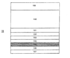
図1に本実施例に記載するLED10の平面模式図を示す。図1に示すのは、LED10を形成するのに利用した図2に示す積層構造体11の表面側からみた平面図である。図3には、図1に示すLED10の破線A−A‘に沿った断面模式図を示す。図4は本発明の半導体発光素子を用いたランプの模式断面図である。
FIG. 1 shows a schematic plan view of the
LED10を形成するための積層構造体11は、(0001)−サファイア基板100上に、次記の各層101〜110 を順次、堆積して構成した。次記する(1)〜(7)項の各層は、一般的な減圧有機金属化学的気相堆積(MOCVD)法で成長させた。特に、GaNバッファ層101は、シーディング(seeding)プロセス(SP)手段(特開2003−243302号公報参照)法により成長させた。
The
(1)アンドープGaNバッファ(buffer)層(層厚=5nm)101
(2)アンドープAlNバッファ(緩衝)層(層厚=15nm)102
(3)珪素(Si)ドープn型GaX1In1−X1N(0≦X1≦1)コンタクト層(層厚=2.5μm、n=8×10¹⁸/cm3)103
(4)Siドープn型GaX2In1−X2N(X1≦X2≦1)クラッド層(層厚=0.5μm、n=4×10¹⁸/cm3)104
(5)Siデルタ(艟)ドーピングGaN障壁層と、Ga0.8In0.2N井戸層とからなる多重量子井戸構造の発光層(積層周期数=5)105
(6)Mgドープp型AlGaNクラッド層(層厚=2.5nm、p=8×10¹⁷/cm3)106
(7)Mgドープp型GaNコンタクト層(層厚=0.2μm、p=2×10¹⁸/cm3)107
(1) Undoped GaN buffer layer (layer thickness = 5 nm) 101
(2) Undoped AlN buffer (buffer) layer (layer thickness = 15 nm) 102
(3) Silicon (Si) doped n-type Ga X1 In 1-X1 N (0 ≦ X 1 ≦ 1) contact layer (layer thickness = 2.5 μm, n = 8 × 10 18 / cm 3 ) 103
(4) Si-doped n-type Ga X2 In 1-X2 N (X 1 ≦ X 2 ≦ 1) cladding layer (layer thickness = 0.5 μm, n = 4 × 10 18 / cm 3 ) 104
(5) Light emitting layer having a multi-quantum well structure composed of a Si delta (艟) -doped GaN barrier layer and a Ga 0.8 In 0.2 N well layer (stacking period number = 5) 105
(6) Mg-doped p-type AlGaN cladding layer (layer thickness = 2.5 nm, p = 8 × 10 17 / cm 3 ) 106
(7) Mg-doped p-type GaN contact layer (layer thickness = 0.2 μm, p = 2 × 10 18 / cm 3 ) 107
LED10用途の積層構造体11の形成を終了した後、サファイア基板100の裏面(積層構造体11を形成したのとは反対側の表面)側をラッピング研削した。その後、より細かい粒径の小さなダイヤモンド微粉を用いて、ラップングした面を精密研磨して、鏡面に仕上げた。これより、サファイア基板100の厚さを、当初の350μmから90μmに減少させた。
After the formation of the
次に、その鏡面に仕上げたサファイア基板100の裏面に、セリウム(Ce)添加YAG蛍光体を含む厚さ約350μmのソーダ石灰ガラス板108を貼り付けた。蛍光体を含む透明なガラス板は、ソーダ石灰ガラスを溶融し、その際、Ce−YAG微粉を添加、分散させて作製した。Ce−YAG微粉は、ガラス板108での含有量が10重量%となる様に添加した。サファイア基板100と、非晶質ガラス基板108とは陽極接合手段で貼り合わせた。貼り合わせは室温で行い、サファイア基板100と非晶質ガラス板108との間に印加した電圧は220Vであった。
Next, a soda-
その後、今度は、積層構造体11の表面側を、公知のフォトリソグラフィー技術及び選択エッチング技術を利用して加工し、n型コンタクト層103の表面を露出させた。露出させたn型コンタクト層103の表面には、クロム(Cr)/チタン(Ti)/金(Au)3層重層構造のn型オーミック電極109を形成した。n型オーミック電極109をなす、各金属層は一般的な真空蒸着手段、電子ビーム蒸着手段を利用して形成した。電極109の最表層は、ワイヤーボンディング(wire bonding)を容易となすために金(Au)膜とした。
Then, this time, the surface side of the
一方、p型GaNコンタクト層107の表面の略前面には、PtとAuとの重層構造からなるp型オーミック電極110を形成した。これらの金属膜は、被着後、ガラス板108の軟化温度を上回らない、軟化温度近傍の温度まで加温処理され、p型コンタクト層107との密着性を向上させた。加熱処理後の冷却時には、熱的ストレスに因り、蛍光体物質を含むガラス板108が剥離しない様に、また、積層構造体11にクラックを発生させない様に、時間をかけて緩やかに除冷した。
On the other hand, a p-
その後、レーザースクライブ法により、素子分割用の割り溝を積層構造体11の表面側に形成した。その後、一般的なブレーカーを利用して、その割り溝に機械的な圧力を及ぼし、個別の素子(チップ)に分割し、III族窒化物半導体発光素子(チップ)10とした。
Thereafter, split grooves for element division were formed on the surface side of the
上記の手順で得たIII族窒化物半導体発光素子チップ10を、導電性で低抵抗のSi単結晶板111にマウントした。チップ10は、マウント位置に金(Au)バンプを形成した後、一般的なフリップチップ(FC)ボンダーを使用してマウントした。Si単結晶板111上には、発光層105からの、波長を約460nmとする青色光を反射しやすくするため、全面にアルミニウム(Al)の反射膜112を形成した。Si単結晶板111と、反対側の表面に蛍光体物資を含むガラス板108とを備えてなるLED10を通常のエポキシ樹脂で封止して、図4に示す断面構造を有する発光ダイオードランプ12を完成させた。
The group III nitride semiconductor light emitting
LED10のn型及びp型オーミック電極109,110間に、順方向に20mAの電流を通流してランプ12を発光させた。通電により、発光層105からの青色の発光と、Ce−YAG蛍光体を含むガラス体108からの黄色の蛍光とが同時に発せられたため、それらの混色により目視で白色を呈するLEDランプ12が提供された。一般的な積分球を使用して測定した白色光の光度は、20ルーメン(lm)/ワット(W)であり、強い光度の白色LEDランプが提供された。
The
本発明のIII族窒化物半導体発光素子は多波長発光素子として利用できる。例えば、赤色、緑色、青色を同時に発光させ白色光とすることもできる。 The group III nitride semiconductor light emitting device of the present invention can be used as a multiwavelength light emitting device. For example, red, green, and blue can be emitted simultaneously to produce white light.
10 III族窒化物半導体発光素子チップ
11 発光素子用積層構造体
12 ランプ
100 結晶基板
101 AlNバッファ層
102 GaNバッファ層
103 n型コンタクト層
104 n型クラッド層
105 発光層
106 p型クラッド層
107 p型コンタクト層
108 蛍光体物質を含む板状体
109 n型オーミック電極
110 p型オーミック電極
111 Si単結晶板
112 反射膜
10 Group III Nitride Semiconductor Light-Emitting
Claims (18)
Priority Applications (1)
| Application Number | Priority Date | Filing Date | Title |
|---|---|---|---|
| JP2005065005A JP2005294820A (en) | 2004-03-12 | 2005-03-09 | Group III nitride semiconductor light emitting device and method for forming the same, lamp using the same, and light source |
Applications Claiming Priority (2)
| Application Number | Priority Date | Filing Date | Title |
|---|---|---|---|
| JP2004070182 | 2004-03-12 | ||
| JP2005065005A JP2005294820A (en) | 2004-03-12 | 2005-03-09 | Group III nitride semiconductor light emitting device and method for forming the same, lamp using the same, and light source |
Publications (2)
| Publication Number | Publication Date |
|---|---|
| JP2005294820A true JP2005294820A (en) | 2005-10-20 |
| JP2005294820A5 JP2005294820A5 (en) | 2008-03-13 |
Family
ID=35327356
Family Applications (1)
| Application Number | Title | Priority Date | Filing Date |
|---|---|---|---|
| JP2005065005A Pending JP2005294820A (en) | 2004-03-12 | 2005-03-09 | Group III nitride semiconductor light emitting device and method for forming the same, lamp using the same, and light source |
Country Status (1)
| Country | Link |
|---|---|
| JP (1) | JP2005294820A (en) |
Cited By (10)
| Publication number | Priority date | Publication date | Assignee | Title |
|---|---|---|---|---|
| JP2007273753A (en) * | 2006-03-31 | 2007-10-18 | Kyocera Corp | Light emitting device and light emitting module |
| JP2009088299A (en) * | 2007-09-29 | 2009-04-23 | Nichia Corp | LIGHT EMITTING ELEMENT AND LIGHT EMITTING DEVICE INCLUDING THE SAME |
| WO2010131402A1 (en) * | 2009-05-15 | 2010-11-18 | 株式会社小糸製作所 | Light-emitting module, method of producing light-emitting module, and lighting fixture unit |
| US7943953B2 (en) | 2006-01-31 | 2011-05-17 | Kyocera Corporation | Light emitting device and light emitting module |
| JP2011216543A (en) * | 2010-03-31 | 2011-10-27 | Ube Industries Ltd | Light emitting diode, substrate for light emitting diode used therein, and method of manufacturing the same |
| JP2011228463A (en) * | 2010-04-20 | 2011-11-10 | Nichia Chem Ind Ltd | Led light source device and manufacturing method for the same |
| WO2012067766A3 (en) * | 2010-11-18 | 2012-07-12 | 3M Innovative Properties Company | Light emitting diode component comprising polysilazane bonding layer |
| JP2014507804A (en) * | 2011-01-28 | 2014-03-27 | ソウル バイオシス カンパニー リミテッド | Wafer level light emitting diode package and method of manufacturing the same |
| JP2016015524A (en) * | 2008-09-24 | 2016-01-28 | フィリップス ルミレッズ ライティング カンパニー リミテッド ライアビリティ カンパニー | LED with controlled angular non-uniformity |
| JP2016076685A (en) * | 2014-10-08 | 2016-05-12 | 株式会社東芝 | Semiconductor light-emitting device and manufacturing method thereof |
Citations (4)
| Publication number | Priority date | Publication date | Assignee | Title |
|---|---|---|---|---|
| JP2000173947A (en) * | 1998-12-07 | 2000-06-23 | Tokai Rika Co Ltd | Plastic package |
| JP2002176200A (en) * | 2000-09-12 | 2002-06-21 | Lumileds Lighting Us Llc | Light-emitting diode with improved light extraction efficiency |
| JP2002289925A (en) * | 2001-03-23 | 2002-10-04 | Citizen Electronics Co Ltd | Light emitting diode |
| JP2003238202A (en) * | 2002-02-14 | 2003-08-27 | Asahi Techno Glass Corp | Crystallized glass for joining anode |
-
2005
- 2005-03-09 JP JP2005065005A patent/JP2005294820A/en active Pending
Patent Citations (4)
| Publication number | Priority date | Publication date | Assignee | Title |
|---|---|---|---|---|
| JP2000173947A (en) * | 1998-12-07 | 2000-06-23 | Tokai Rika Co Ltd | Plastic package |
| JP2002176200A (en) * | 2000-09-12 | 2002-06-21 | Lumileds Lighting Us Llc | Light-emitting diode with improved light extraction efficiency |
| JP2002289925A (en) * | 2001-03-23 | 2002-10-04 | Citizen Electronics Co Ltd | Light emitting diode |
| JP2003238202A (en) * | 2002-02-14 | 2003-08-27 | Asahi Techno Glass Corp | Crystallized glass for joining anode |
Cited By (11)
| Publication number | Priority date | Publication date | Assignee | Title |
|---|---|---|---|---|
| US7943953B2 (en) | 2006-01-31 | 2011-05-17 | Kyocera Corporation | Light emitting device and light emitting module |
| JP2007273753A (en) * | 2006-03-31 | 2007-10-18 | Kyocera Corp | Light emitting device and light emitting module |
| JP2009088299A (en) * | 2007-09-29 | 2009-04-23 | Nichia Corp | LIGHT EMITTING ELEMENT AND LIGHT EMITTING DEVICE INCLUDING THE SAME |
| JP2016015524A (en) * | 2008-09-24 | 2016-01-28 | フィリップス ルミレッズ ライティング カンパニー リミテッド ライアビリティ カンパニー | LED with controlled angular non-uniformity |
| WO2010131402A1 (en) * | 2009-05-15 | 2010-11-18 | 株式会社小糸製作所 | Light-emitting module, method of producing light-emitting module, and lighting fixture unit |
| JP2011216543A (en) * | 2010-03-31 | 2011-10-27 | Ube Industries Ltd | Light emitting diode, substrate for light emitting diode used therein, and method of manufacturing the same |
| JP2011228463A (en) * | 2010-04-20 | 2011-11-10 | Nichia Chem Ind Ltd | Led light source device and manufacturing method for the same |
| WO2012067766A3 (en) * | 2010-11-18 | 2012-07-12 | 3M Innovative Properties Company | Light emitting diode component comprising polysilazane bonding layer |
| US9041034B2 (en) | 2010-11-18 | 2015-05-26 | 3M Innovative Properties Company | Light emitting diode component comprising polysilazane bonding layer |
| JP2014507804A (en) * | 2011-01-28 | 2014-03-27 | ソウル バイオシス カンパニー リミテッド | Wafer level light emitting diode package and method of manufacturing the same |
| JP2016076685A (en) * | 2014-10-08 | 2016-05-12 | 株式会社東芝 | Semiconductor light-emitting device and manufacturing method thereof |
Similar Documents
| Publication | Publication Date | Title |
|---|---|---|
| CN100405619C (en) | Nitride semiconductor device with supporting substrate and method for manufacturing the same | |
| US7242030B2 (en) | Quantum dot/quantum well light emitting diode | |
| EP1921686A2 (en) | Semiconductor light emitting device and method for manufacturing same | |
| US20070018178A1 (en) | Vertical electrode structure of gallium nitride based light emitting diode | |
| US20080042150A1 (en) | White Light Emitting Device and Method for Manufacturing the Same | |
| JP3476611B2 (en) | Multicolor light emitting device and display device using the same | |
| JPWO2017217486A1 (en) | Phosphor element and lighting device | |
| JP4586802B2 (en) | Light emitting diode element, light emitting diode substrate, and method for manufacturing light emitting diode element | |
| JP2005294820A (en) | Group III nitride semiconductor light emitting device and method for forming the same, lamp using the same, and light source | |
| US7576365B2 (en) | Group III nitride semiconductor light-emitting device, forming method thereof, lamp and light source using same | |
| JP2000216434A (en) | Light emitting diode and method of forming the same | |
| JPH1056203A (en) | Light emitting element | |
| TWI231054B (en) | Light-emitting diode and its manufacturing method | |
| JP4843235B2 (en) | Group III nitride semiconductor light emitting device manufacturing method | |
| TWI302755B (en) | Group iii nitride semiconductor light-emitting device, forming method thereof,and lamp using same | |
| JP2010153561A (en) | Light emitting device | |
| JP2005072527A (en) | Light emitting element and its manufacturing method | |
| CN208986022U (en) | A red light flip chip | |
| JP2018163816A (en) | Phosphor element and lighting device | |
| JP4978877B2 (en) | Light emitting device manufacturing method and light emitting device | |
| JP4689315B2 (en) | Pn junction type compound semiconductor light emitting device and manufacturing method thereof | |
| TWI884669B (en) | Light emitting diode structure | |
| TWI281757B (en) | Group III nitride semiconductor light-emitting device and producing method thereof | |
| JP7011195B2 (en) | Luminescent device | |
| CN111365685A (en) | A light-emitting device with high red light brightness and high reliability |
Legal Events
| Date | Code | Title | Description |
|---|---|---|---|
| A521 | Request for written amendment filed |
Free format text: JAPANESE INTERMEDIATE CODE: A523 Effective date: 20080129 |
|
| A621 | Written request for application examination |
Free format text: JAPANESE INTERMEDIATE CODE: A621 Effective date: 20080129 |
|
| A977 | Report on retrieval |
Free format text: JAPANESE INTERMEDIATE CODE: A971007 Effective date: 20100720 |
|
| A131 | Notification of reasons for refusal |
Free format text: JAPANESE INTERMEDIATE CODE: A131 Effective date: 20100727 |
|
| A521 | Request for written amendment filed |
Free format text: JAPANESE INTERMEDIATE CODE: A523 Effective date: 20100922 |
|
| RD02 | Notification of acceptance of power of attorney |
Free format text: JAPANESE INTERMEDIATE CODE: A7422 Effective date: 20100922 |
|
| A131 | Notification of reasons for refusal |
Free format text: JAPANESE INTERMEDIATE CODE: A131 Effective date: 20101207 |
|
| A02 | Decision of refusal |
Free format text: JAPANESE INTERMEDIATE CODE: A02 Effective date: 20110405 |