JP2005294813A - Pn junction type group iii nitride semiconductor light-emitting device - Google Patents
Pn junction type group iii nitride semiconductor light-emitting device Download PDFInfo
- Publication number
- JP2005294813A JP2005294813A JP2005061867A JP2005061867A JP2005294813A JP 2005294813 A JP2005294813 A JP 2005294813A JP 2005061867 A JP2005061867 A JP 2005061867A JP 2005061867 A JP2005061867 A JP 2005061867A JP 2005294813 A JP2005294813 A JP 2005294813A
- Authority
- JP
- Japan
- Prior art keywords
- layer
- type
- iii nitride
- nitride semiconductor
- group iii
- Prior art date
- Legal status (The legal status is an assumption and is not a legal conclusion. Google has not performed a legal analysis and makes no representation as to the accuracy of the status listed.)
- Pending
Links
- 239000004065 semiconductor Substances 0.000 title claims abstract description 55
- 150000004767 nitrides Chemical class 0.000 title claims abstract description 51
- 230000004888 barrier function Effects 0.000 claims abstract description 104
- 239000000758 substrate Substances 0.000 claims abstract description 35
- 239000013078 crystal Substances 0.000 claims abstract description 29
- 238000005253 cladding Methods 0.000 claims description 73
- 239000012535 impurity Substances 0.000 claims description 43
- 230000007423 decrease Effects 0.000 claims description 5
- 239000006185 dispersion Substances 0.000 abstract 1
- 239000010410 layer Substances 0.000 description 450
- 229910002601 GaN Inorganic materials 0.000 description 35
- JMASRVWKEDWRBT-UHFFFAOYSA-N Gallium nitride Chemical compound [Ga]#N JMASRVWKEDWRBT-UHFFFAOYSA-N 0.000 description 33
- 238000000034 method Methods 0.000 description 17
- IJGRMHOSHXDMSA-UHFFFAOYSA-N Atomic nitrogen Chemical compound N#N IJGRMHOSHXDMSA-UHFFFAOYSA-N 0.000 description 14
- 239000000463 material Substances 0.000 description 14
- 239000000969 carrier Substances 0.000 description 9
- 238000006243 chemical reaction Methods 0.000 description 9
- 239000000203 mixture Substances 0.000 description 9
- 229910052738 indium Inorganic materials 0.000 description 8
- PXHVJJICTQNCMI-UHFFFAOYSA-N Nickel Chemical compound [Ni] PXHVJJICTQNCMI-UHFFFAOYSA-N 0.000 description 7
- APFVFJFRJDLVQX-UHFFFAOYSA-N indium atom Chemical compound [In] APFVFJFRJDLVQX-UHFFFAOYSA-N 0.000 description 7
- 229910052757 nitrogen Inorganic materials 0.000 description 7
- 239000010980 sapphire Substances 0.000 description 7
- 229910052594 sapphire Inorganic materials 0.000 description 7
- 239000010931 gold Substances 0.000 description 6
- 238000002488 metal-organic chemical vapour deposition Methods 0.000 description 6
- XCZXGTMEAKBVPV-UHFFFAOYSA-N trimethylgallium Chemical compound C[Ga](C)C XCZXGTMEAKBVPV-UHFFFAOYSA-N 0.000 description 6
- XUIMIQQOPSSXEZ-UHFFFAOYSA-N Silicon Chemical compound [Si] XUIMIQQOPSSXEZ-UHFFFAOYSA-N 0.000 description 5
- RNQKDQAVIXDKAG-UHFFFAOYSA-N aluminum gallium Chemical compound [Al].[Ga] RNQKDQAVIXDKAG-UHFFFAOYSA-N 0.000 description 5
- 238000009792 diffusion process Methods 0.000 description 5
- 239000007789 gas Substances 0.000 description 5
- 229910052710 silicon Inorganic materials 0.000 description 5
- 239000010703 silicon Substances 0.000 description 5
- JLTRXTDYQLMHGR-UHFFFAOYSA-N trimethylaluminium Chemical compound C[Al](C)C JLTRXTDYQLMHGR-UHFFFAOYSA-N 0.000 description 5
- 238000001947 vapour-phase growth Methods 0.000 description 5
- QGZKDVFQNNGYKY-UHFFFAOYSA-N Ammonia Chemical compound N QGZKDVFQNNGYKY-UHFFFAOYSA-N 0.000 description 4
- 230000000052 comparative effect Effects 0.000 description 4
- 230000003247 decreasing effect Effects 0.000 description 4
- 238000005304 joining Methods 0.000 description 4
- 239000011777 magnesium Substances 0.000 description 4
- 229910052751 metal Inorganic materials 0.000 description 4
- 239000002184 metal Substances 0.000 description 4
- 239000010936 titanium Substances 0.000 description 4
- 239000000470 constituent Substances 0.000 description 3
- 238000010586 diagram Methods 0.000 description 3
- 230000000694 effects Effects 0.000 description 3
- 229910052733 gallium Inorganic materials 0.000 description 3
- PCHJSUWPFVWCPO-UHFFFAOYSA-N gold Chemical compound [Au] PCHJSUWPFVWCPO-UHFFFAOYSA-N 0.000 description 3
- 229910052737 gold Inorganic materials 0.000 description 3
- 229910021478 group 5 element Inorganic materials 0.000 description 3
- NJPPVKZQTLUDBO-UHFFFAOYSA-N novaluron Chemical compound C1=C(Cl)C(OC(F)(F)C(OC(F)(F)F)F)=CC=C1NC(=O)NC(=O)C1=C(F)C=CC=C1F NJPPVKZQTLUDBO-UHFFFAOYSA-N 0.000 description 3
- ZOXJGFHDIHLPTG-UHFFFAOYSA-N Boron Chemical compound [B] ZOXJGFHDIHLPTG-UHFFFAOYSA-N 0.000 description 2
- GYHNNYVSQQEPJS-UHFFFAOYSA-N Gallium Chemical compound [Ga] GYHNNYVSQQEPJS-UHFFFAOYSA-N 0.000 description 2
- OAICVXFJPJFONN-UHFFFAOYSA-N Phosphorus Chemical compound [P] OAICVXFJPJFONN-UHFFFAOYSA-N 0.000 description 2
- RTAQQCXQSZGOHL-UHFFFAOYSA-N Titanium Chemical compound [Ti] RTAQQCXQSZGOHL-UHFFFAOYSA-N 0.000 description 2
- 229910052782 aluminium Inorganic materials 0.000 description 2
- XAGFODPZIPBFFR-UHFFFAOYSA-N aluminium Chemical compound [Al] XAGFODPZIPBFFR-UHFFFAOYSA-N 0.000 description 2
- 229910052796 boron Inorganic materials 0.000 description 2
- 239000011575 calcium Substances 0.000 description 2
- 230000008859 change Effects 0.000 description 2
- 150000001875 compounds Chemical class 0.000 description 2
- 230000007547 defect Effects 0.000 description 2
- 229910001873 dinitrogen Inorganic materials 0.000 description 2
- 238000009826 distribution Methods 0.000 description 2
- HZXMRANICFIONG-UHFFFAOYSA-N gallium phosphide Chemical compound [Ga]#P HZXMRANICFIONG-UHFFFAOYSA-N 0.000 description 2
- 238000010438 heat treatment Methods 0.000 description 2
- 150000004678 hydrides Chemical class 0.000 description 2
- 230000006698 induction Effects 0.000 description 2
- 238000004519 manufacturing process Methods 0.000 description 2
- 229910052759 nickel Inorganic materials 0.000 description 2
- 229910052698 phosphorus Inorganic materials 0.000 description 2
- 239000011574 phosphorus Substances 0.000 description 2
- 239000002994 raw material Substances 0.000 description 2
- 239000011669 selenium Substances 0.000 description 2
- HBMJWWWQQXIZIP-UHFFFAOYSA-N silicon carbide Chemical compound [Si+]#[C-] HBMJWWWQQXIZIP-UHFFFAOYSA-N 0.000 description 2
- 238000004381 surface treatment Methods 0.000 description 2
- 229910052719 titanium Inorganic materials 0.000 description 2
- IBEFSUTVZWZJEL-UHFFFAOYSA-N trimethylindium Chemical compound C[In](C)C IBEFSUTVZWZJEL-UHFFFAOYSA-N 0.000 description 2
- 229910018072 Al 2 O 3 Inorganic materials 0.000 description 1
- OYPRJOBELJOOCE-UHFFFAOYSA-N Calcium Chemical compound [Ca] OYPRJOBELJOOCE-UHFFFAOYSA-N 0.000 description 1
- 229910005540 GaP Inorganic materials 0.000 description 1
- UFHFLCQGNIYNRP-UHFFFAOYSA-N Hydrogen Chemical compound [H][H] UFHFLCQGNIYNRP-UHFFFAOYSA-N 0.000 description 1
- WHXSMMKQMYFTQS-UHFFFAOYSA-N Lithium Chemical compound [Li] WHXSMMKQMYFTQS-UHFFFAOYSA-N 0.000 description 1
- FYYHWMGAXLPEAU-UHFFFAOYSA-N Magnesium Chemical compound [Mg] FYYHWMGAXLPEAU-UHFFFAOYSA-N 0.000 description 1
- BUGBHKTXTAQXES-UHFFFAOYSA-N Selenium Chemical compound [Se] BUGBHKTXTAQXES-UHFFFAOYSA-N 0.000 description 1
- BLRPTPMANUNPDV-UHFFFAOYSA-N Silane Chemical compound [SiH4] BLRPTPMANUNPDV-UHFFFAOYSA-N 0.000 description 1
- ATJFFYVFTNAWJD-UHFFFAOYSA-N Tin Chemical compound [Sn] ATJFFYVFTNAWJD-UHFFFAOYSA-N 0.000 description 1
- XLOMVQKBTHCTTD-UHFFFAOYSA-N Zinc monoxide Chemical compound [Zn]=O XLOMVQKBTHCTTD-UHFFFAOYSA-N 0.000 description 1
- 230000009471 action Effects 0.000 description 1
- 230000003213 activating effect Effects 0.000 description 1
- 239000000956 alloy Substances 0.000 description 1
- 229910045601 alloy Inorganic materials 0.000 description 1
- 229910021529 ammonia Inorganic materials 0.000 description 1
- 238000004458 analytical method Methods 0.000 description 1
- 238000000137 annealing Methods 0.000 description 1
- 229910052785 arsenic Inorganic materials 0.000 description 1
- RQNWIZPPADIBDY-UHFFFAOYSA-N arsenic atom Chemical compound [As] RQNWIZPPADIBDY-UHFFFAOYSA-N 0.000 description 1
- NWAIGJYBQQYSPW-UHFFFAOYSA-N azanylidyneindigane Chemical compound [In]#N NWAIGJYBQQYSPW-UHFFFAOYSA-N 0.000 description 1
- 230000008901 benefit Effects 0.000 description 1
- 230000015572 biosynthetic process Effects 0.000 description 1
- FFBGYFUYJVKRNV-UHFFFAOYSA-N boranylidynephosphane Chemical compound P#B FFBGYFUYJVKRNV-UHFFFAOYSA-N 0.000 description 1
- 229910052791 calcium Inorganic materials 0.000 description 1
- 239000012159 carrier gas Substances 0.000 description 1
- 238000005229 chemical vapour deposition Methods 0.000 description 1
- 238000001816 cooling Methods 0.000 description 1
- AJNVQOSZGJRYEI-UHFFFAOYSA-N digallium;oxygen(2-) Chemical compound [O-2].[O-2].[O-2].[Ga+3].[Ga+3] AJNVQOSZGJRYEI-UHFFFAOYSA-N 0.000 description 1
- 239000002019 doping agent Substances 0.000 description 1
- 239000007772 electrode material Substances 0.000 description 1
- 238000000921 elemental analysis Methods 0.000 description 1
- 238000005530 etching Methods 0.000 description 1
- 238000000605 extraction Methods 0.000 description 1
- 229910001195 gallium oxide Inorganic materials 0.000 description 1
- 229910052732 germanium Inorganic materials 0.000 description 1
- GNPVGFCGXDBREM-UHFFFAOYSA-N germanium atom Chemical compound [Ge] GNPVGFCGXDBREM-UHFFFAOYSA-N 0.000 description 1
- 229910021480 group 4 element Inorganic materials 0.000 description 1
- 229910021476 group 6 element Inorganic materials 0.000 description 1
- 229910052736 halogen Inorganic materials 0.000 description 1
- 150000002367 halogens Chemical class 0.000 description 1
- 125000005842 heteroatom Chemical group 0.000 description 1
- 238000002347 injection Methods 0.000 description 1
- 239000007924 injection Substances 0.000 description 1
- 238000010030 laminating Methods 0.000 description 1
- 229910052744 lithium Inorganic materials 0.000 description 1
- 229910052749 magnesium Inorganic materials 0.000 description 1
- 238000002844 melting Methods 0.000 description 1
- 230000008018 melting Effects 0.000 description 1
- 150000002739 metals Chemical class 0.000 description 1
- -1 nitride compound Chemical class 0.000 description 1
- 238000000059 patterning Methods 0.000 description 1
- 230000000737 periodic effect Effects 0.000 description 1
- 230000008569 process Effects 0.000 description 1
- 238000010926 purge Methods 0.000 description 1
- 239000010453 quartz Substances 0.000 description 1
- 238000001004 secondary ion mass spectrometry Methods 0.000 description 1
- 229910052711 selenium Inorganic materials 0.000 description 1
- 229910000077 silane Inorganic materials 0.000 description 1
- VYPSYNLAJGMNEJ-UHFFFAOYSA-N silicon dioxide Inorganic materials O=[Si]=O VYPSYNLAJGMNEJ-UHFFFAOYSA-N 0.000 description 1
- 239000002356 single layer Substances 0.000 description 1
- 230000000087 stabilizing effect Effects 0.000 description 1
- 239000000126 substance Substances 0.000 description 1
- 229910052714 tellurium Inorganic materials 0.000 description 1
- PORWMNRCUJJQNO-UHFFFAOYSA-N tellurium atom Chemical compound [Te] PORWMNRCUJJQNO-UHFFFAOYSA-N 0.000 description 1
Images


Landscapes
- Led Devices (AREA)
Abstract
Description
本発明は、結晶基板上に形成された、III族窒化物半導体からなるn型クラッド層とp型クラッド層との間に、III族窒化物半導体からなる井戸層と障壁層とを交互に数周期に亘り積層させてなる多重量子井戸構造の発光層を備えたpn接合型III族窒化物半導体発光素子に関するものである。 In the present invention, a number of well layers and barrier layers made of a group III nitride semiconductor are alternately arranged between an n-type cladding layer made of a group III nitride semiconductor and a p-type cladding layer formed on a crystal substrate. The present invention relates to a pn-junction group III nitride semiconductor light emitting device having a light emitting layer having a multiple quantum well structure laminated over a period.
従来から、III族窒化物半導体は、短波長の可視光を放射する発光ダイオード(LED)等のpn接合型ヘテロ(hetero)接合構造のIII族窒化物半導体発光素子を構成するための機能材料として利用されている(特許文献1参照)。例えば近紫外帯、青色帯、或いは緑色帯の発光を呈するLEDを構成するのに際し、n形またはp形の窒化アルミニウム・ガリウム(組成式AlXGaYN:0≦X,Y≦1、X+Y=1)は、クラッド(clad)層を構成するのに利用されている(特許文献2参照)。また、窒化ガリウム・インジウム(組成式GaYInZN:0≦Y,Z≦1、Y+Z=1)は、活性層(発光層)を構成するのに利用されている(特許文献3参照)。 Conventionally, a group III nitride semiconductor has been used as a functional material for forming a group III nitride semiconductor light emitting device having a pn junction type hetero junction structure such as a light emitting diode (LED) that emits short-wavelength visible light. (See Patent Document 1). For example, when an LED that emits light in the near ultraviolet band, the blue band, or the green band is constructed, an n-type or p-type aluminum gallium nitride (compositional formula Al X Ga Y N: 0 ≦ X, Y ≦ 1, X + Y = 1) is used to form a clad layer (see Patent Document 2). Further, gallium indium nitride (compositional formula Ga Y In Z N: 0 ≦ Y, Z ≦ 1, Y + Z = 1) , the active layer is utilized to construct the (light-emitting layer) (see Patent Document 3) .
従来において、発光層を、数量的に単一のGaYInZN(0≦Y,Z≦1、Y+Z=1)層から構成する技術例が開示されている(特許文献3参照)。また、発光層を量子井戸構造と称する超格子構造から構成する例も公知である(特許文献4参照)。量子井戸構造とは、障壁(barrier)層と井戸(well)層とを交互に積層させた、周期的積層構造を指している(特許文献5参照)。例えば、Ga0.7In0.3N層を井戸層とし、窒化ガリウム(GaN)を障壁層として多重量子井戸構造の発光層を構成する実施例が開示されている(特許文献4の[実施例1]参照)。
しかし、上記の従来技術例では、発光層の一端側、他端側が必ずしも障壁層に限定されておらず、何れか一方が井戸層の場合は、その井戸層を経由してクラッド層へのキャリア(電子)の拡散が発生しやすく、それだけ発光出力が低下してしまうという問題点を有していた。 However, in the above prior art example, one end side and the other end side of the light emitting layer are not necessarily limited to the barrier layer, and when either one is a well layer, carriers to the cladding layer via the well layer There is a problem that (electron) diffusion is likely to occur, and the light emission output is reduced accordingly.
また、特にp型クラッド層に接する発光層の多端側に障壁層が形成されていても、その障壁層の層厚が十分でなく、n型クラッド層側から注入されたキャリアのp型クラッド層側への流入を抑制することができず、その影響で発光出力が低下してしまうという問題点も有していた。 In particular, even if a barrier layer is formed on the multi-end side of the light emitting layer in contact with the p-type cladding layer, the layer thickness of the barrier layer is not sufficient, and the p-type cladding layer of carriers injected from the n-type cladding layer side Inflow to the side cannot be suppressed, and the light emission output is lowered due to the influence.
本発明は、上記に鑑みてなされたもので、発光層を多重量子井戸構造とした場合でも、クラッド層へのキャリアの拡散を抑制し、発光出力を大幅に向上させることができるpn接合型III族窒化物半導体発光素子を提供することを目的とする。 The present invention has been made in view of the above, and even when the light emitting layer has a multiple quantum well structure, pn junction type III that can suppress the diffusion of carriers to the cladding layer and can greatly improve the light emission output. An object is to provide a group nitride semiconductor light emitting device.
1)上記目的を達成するために、第1の発明は、結晶基板上に形成された、III族窒化物半導体からなるn型クラッド層とp型クラッド層との間に、III族窒化物半導体からなる井戸層と障壁層とを交互に数周期に亘り積層させてなる多重量子井戸構造の発光層を備えたpn接合型III族窒化物半導体発光素子において、上記発光層は、n型クラッド層に最も近接して対峙する一端層、及びp型クラッド層に最も近接して対峙する他端層とが共に障壁層であり、その他端層は他の障壁層よりも層厚が大である、ことを特徴としている。 1) To achieve the above object, according to a first aspect of the present invention, there is provided a group III nitride semiconductor between an n-type cladding layer made of a group III nitride semiconductor and a p-type cladding layer formed on a crystal substrate. In a pn-junction group III nitride semiconductor light emitting device having a light emitting layer having a multiple quantum well structure in which well layers and barrier layers made of a material are alternately stacked for several periods, the light emitting layer is an n type cladding layer. Both the one end layer facing closest to the other end layer and the other end layer facing closest to the p-type cladding layer are barrier layers, and the other end layer has a larger layer thickness than the other barrier layers. It is characterized by that.
2)第2の発明は、上記した1)項に記載の発明の構成に加えて、上記障壁層の各層厚を、一端層から他端層に向けて漸次大とした、ことを特徴としている。 2) The second invention is characterized in that, in addition to the configuration of the invention described in the above item 1), each layer thickness of the barrier layer is gradually increased from one end layer to the other end layer. .
3)第3の発明は、上記した1)項または2)項に記載の発明の構成に加えて、上記他端層は、不純物濃度が井戸層と接合する側で低く、層の中央部で最も高く、中央部よりp型クラッド層に向けて漸次減少する、ことを特徴としている。 3) In the third aspect of the invention, in addition to the configuration of the invention described in the above item 1) or 2), the other end layer has a low impurity concentration on the side where the well layer is joined, It is the highest and gradually decreases from the center toward the p-type cladding layer.
4)第4の発明は、上記した1)項から3)項の何れか1項に記載の発明の構成に加えて、上記他端層には、不純物が故意に添加されていないアンドープの井戸層が接合されている、ことを特徴としている。 4) The fourth invention is an undoped well in which no impurity is intentionally added to the other end layer in addition to the configuration of the invention described in any one of 1) to 3) above. It is characterized in that the layers are joined.
本発明では、多重量子井戸構造の発光層において、その両端をなす層を何れも障壁層としたので、クラッド層へのキャリアの拡散を抑制することができ、井戸層内にキャリアを閉じ込める作用を有するため、発光出力を向上させることができる。 In the present invention, in the light emitting layer having a multiple quantum well structure, since both of the layers forming the both ends are barrier layers, it is possible to suppress the diffusion of carriers into the cladding layer and to confine carriers in the well layer. Therefore, the light emission output can be improved.
また、多重量子井戸構造の発光層の両端をなす障壁層のうち、p型クラッド層に接する他端層を、他の障壁層より層厚を大としたので、n型クラッド層側から注入されるキャリア(電子)のp型クラッド層側への流入を抑制することができ、発光出力を高くすることができる。 In addition, among the barrier layers forming both ends of the light emitting layer having a multiple quantum well structure, the other end layer in contact with the p-type cladding layer is made thicker than the other barrier layers, so that it is injected from the n-type cladding layer side. Inflow of carriers (electrons) to the p-type cladding layer side can be suppressed, and the light emission output can be increased.
さらに、本発明によれば、発光効率を1.5倍程度向上させることができ、したがって、LEDランプの発光出力及び電光変換効率ともに1.5倍程度向上させることができ、省エネルギーに寄与することができる。 Furthermore, according to the present invention, the light emission efficiency can be improved by about 1.5 times, and therefore the light emission output and the electro-optic conversion efficiency of the LED lamp can be improved by about 1.5 times, contributing to energy saving. Can do.
また、本発明では、障壁層の各層厚を、一端層から他端層に向けて漸次大としたので、井戸層へのキャリアの閉じ込めを更に強めることができる。なお、この場合、障壁層の各層厚は、各井戸層からの発光波長が変化しない程度とするのが好ましい。 In the present invention, since the thickness of each barrier layer is gradually increased from one end layer to the other end layer, the confinement of carriers in the well layer can be further enhanced. In this case, it is preferable that the thickness of each barrier layer is set such that the emission wavelength from each well layer does not change.
また、他端層について、不純物濃度が井戸層と接合する側で低く、層の中央部で最も高く、中央部よりp型クラッド層に向けて漸次減少するようにしたので、他端層に接する井戸層に与える環境と、多重量子井戸層への正孔の注入効率との両立を図ることができる。 Further, the other end layer has a low impurity concentration on the side joining the well layer, is highest at the center of the layer, and gradually decreases from the center toward the p-type cladding layer. It is possible to achieve both the environment given to the well layer and the efficiency of hole injection into the multiple quantum well layer.
さらに、他端層には、不純物が故意に添加されていないアンドープの井戸層が接合されているようにすることで、井戸層の結晶性を向上させることができ、発光効率を高めることができる。 Furthermore, by connecting an undoped well layer to which no impurity is intentionally added to the other end layer, the crystallinity of the well layer can be improved and the luminous efficiency can be increased. .
以下にこの発明の実施の形態を詳細に説明する。 Embodiments of the present invention will be described in detail below.
本願発明では、結晶基板上、特に、単結晶基板上に形成されたn型またはp型の導電型のIII族窒化物半導体層を利用して、pn接合型III族窒化物半導体発光素子を構成する。 In the present invention, a pn-junction group III nitride semiconductor light-emitting device is formed using an n-type or p-type conductivity type group III nitride semiconductor layer formed on a crystal substrate, particularly a single crystal substrate. To do.
すなわち、本発明のpn接合型III族窒化物半導体発光素子は、結晶基板上に形成された、III族窒化物半導体からなるn型クラッド層とp型クラッド層との間に、III族窒化物半導体からなる井戸層と障壁層とを交互に数周期に亘り積層させてなる多重量子井戸構造の発光層を備え、その発光層は、n型クラッド層に最も近接して対峙する一端層、及びp型クラッド層に最も近接して対峙する他端層とが共に障壁層であり、その他端層は他の障壁層よりも層厚が大となっている。 That is, the pn junction group III nitride semiconductor light-emitting device of the present invention includes a group III nitride formed between a n-type cladding layer made of a group III nitride semiconductor and a p-type cladding layer formed on a crystal substrate. A light emitting layer having a multiple quantum well structure in which a well layer and a barrier layer made of a semiconductor are alternately laminated for several cycles, and the light emitting layer has one end layer facing the n-type cladding layer closest to the n-type cladding layer; The other end layer facing the p-type cladding layer closest to the p-type cladding layer is a barrier layer, and the other end layer has a larger thickness than the other barrier layers.
なお、結晶基板により近い方のクラッド層をn型としてもよいし、逆にp型としてもよい。 The clad layer closer to the crystal substrate may be n-type, or vice versa.
III族窒化物半導体層を形成する際に、基板とする単結晶材料として、融点が比較的高く、耐熱性のあるサファイア(α−Al2O3単結晶)や酸化亜鉛(ZnO)、酸化ガリウム・リチウム(組成式LiGaO2)等の酸化物単結晶材料、また珪素(Si)単結晶(シリコン)や立方晶、六方晶結晶型の炭化珪素(SiC)等のIV族半導体単結晶、さらにはリン化ガリウム(GaP)等のIII−V族化合物半導体単結晶材料を利用できる。発光層からの発光を透過できる、光学的に透明な単結晶材料は基板として有効に利用できる。 As a single crystal material for forming a group III nitride semiconductor layer, sapphire (α-Al 2 O 3 single crystal), zinc oxide (ZnO), gallium oxide having a relatively high melting point and heat resistance are used. Oxide single crystal materials such as lithium (compositional formula LiGaO 2 ), group IV semiconductor single crystals such as silicon (Si) single crystal (silicon), cubic and hexagonal crystal silicon carbide (SiC), and A III-V compound semiconductor single crystal material such as gallium phosphide (GaP) can be used. An optically transparent single crystal material that can transmit light emitted from the light emitting layer can be effectively used as a substrate.
結晶基板上に設けるn型及びp型のIII族窒化物半導体層(クラッド層)は、組成式AlXGaYInZN1-aMa(0≦X≦1、0≦Y≦1、0≦Z≦1で且つ、X+Y+Z=1。記号Mは窒素とは別の第V族元素を表し、0≦a<1である。)から構成する。結晶基板と、その上に形成するIII族窒化物半導体層(クラッド層)とで格子ミスマッチがある場合、そのミスマッチを緩和して、結晶性に優れる上層をもたらす低温緩衝層或いは高温緩衝層を介在させて積層するのが得策である。緩衝層は、例えば、窒化アルミニウム・ガリウム(組成式AlXGaYN:0≦X≦1,0≦Y≦1で且つ、X+Y=1)から構成できる。 The n-type and p-type group III nitride semiconductor layers (cladding layers) provided on the crystal substrate have a composition formula of Al x Ga y In z N 1-a M a (0 ≦ X ≦ 1, 0 ≦ Y ≦ 1, 0 ≦ Z ≦ 1 and X + Y + Z = 1, the symbol M represents a Group V element different from nitrogen, and 0 ≦ a <1). When there is a lattice mismatch between the crystal substrate and the group III nitride semiconductor layer (cladding layer) formed on the crystal substrate, a low-temperature buffer layer or a high-temperature buffer layer that relaxes the mismatch and provides an upper layer with excellent crystallinity is interposed It is a good idea to stack them together. The buffer layer can be made of, for example, aluminum gallium nitride (compositional formula Al x Ga y N: 0 ≦ X ≦ 1, 0 ≦ Y ≦ 1 and X + Y = 1).
n型及びp型のクラッド層を、同一の組成比のIII族窒化物半導体材料から構成する必要は必ずしもない。例えば、n型のクラッド層を窒化ガリウム(GaN)から構成し、p型のクラッド層を窒化アルミニウム・ガリウム(AlXGaYN)から構成できる。n型及びp型のクラッド層は、発光層をなす量子井戸構造を構成する障壁層よりも禁止帯幅を大とするIII族窒化物半導体から構成するのが好ましい。 The n-type and p-type cladding layers are not necessarily made of a group III nitride semiconductor material having the same composition ratio. For example, the n-type cladding layer can be composed of gallium nitride (GaN), and the p-type cladding layer can be composed of aluminum gallium nitride (Al x Ga y N). The n-type and p-type cladding layers are preferably made of a group III nitride semiconductor having a larger forbidden band than the barrier layer constituting the quantum well structure forming the light emitting layer.
n型のクラッド層とp型のクラッド層との中間に配置する発光層は、III族窒化物半導体からなる井戸層と障壁層とを交互に数周期に亘り積層させてなる多重量子井戸構造とし、その両端層(一端層及び他端層)は共に障壁層から構成する。n型及びp型クラッド層へのキャリアの拡散をより良く防止する構成とするためである。このように本発明の発光層を構成する各層のうち、n型クラッド層に最も近接して対峙する一端層、及びp型クラッド層に最も近接して対峙する他端層は、何れも障壁層として形成する。 The light emitting layer disposed between the n-type cladding layer and the p-type cladding layer has a multiple quantum well structure in which a well layer and a barrier layer made of a group III nitride semiconductor are alternately stacked over several cycles. The both end layers (one end layer and the other end layer) are both composed of a barrier layer. This is to better prevent carrier diffusion into the n-type and p-type cladding layers. As described above, among the layers constituting the light emitting layer of the present invention, the one end layer facing the n-type cladding layer closest to the n-type cladding layer and the other end layer facing the p-type cladding layer closest to each other are both barrier layers. Form as.
井戸層は、障壁層よりも禁止帯幅を小とするIII族窒化物半導体から構成する。例えば、窒化ガリウム・インジウム(GaYInZN:0≦Y≦1、0≦Z≦1で且つ、Y+Z=1)から構成する。GaYInZNのインジウム組成比(ガリウム組成比)は、所望の波長の発光が得られる様に適宣、選択する。近紫外帯、青色帯、或いは緑色帯の短波長の発光を期す発光素子の発光層は、インジウム組成比を、大凡、0.40(=40%)以下、望ましくは0.25とするGaYInZN(0.25≦Z≦0.40で且つ、Y+Z=1)から構成できる。 The well layer is made of a group III nitride semiconductor having a forbidden band width smaller than that of the barrier layer. For example, it is made of gallium nitride indium (Ga Y In Z N: 0 ≦ Y ≦ 1, 0 ≦ Z ≦ 1 and Y + Z = 1). The indium composition ratio (gallium composition ratio) of Ga Y In Z N is appropriately selected so that light emission with a desired wavelength can be obtained. The light emitting layer of the light emitting device that emits light of short wavelength in the near ultraviolet band, the blue band, or the green band has a indium composition ratio of about 0.40 (= 40%) or less, preferably 0.25 Ga Y In ZN (0.25 ≦ Z ≦ 0.40 and Y + Z = 1) can be used.
多重量子井戸構造の発光層を構成する井戸層は、また、例えば、窒化・リン化ガリウム(GaN1-aPa:0≦a<1)等の窒素と窒素以外の第V族元素を含むIII族窒化物半導体から構成できる。GaN1-aPaでは、リン(P)組成比(=a)に依存して(換言すれば、窒素(N)組成比(=1−a)に依存して)、禁止帯幅は急激に変化する。このバンドボーイング(band bowing)性を利用して、GaN1-aPaからは、紫外帯から赤色帯に亘る発光を放射できる井戸層を形成できる。 The well layer constituting the light emitting layer having a multiple quantum well structure also contains, for example, nitrogen and group V elements other than nitrogen, such as gallium nitride / gallium phosphide (GaN 1-a P a : 0 ≦ a <1). It can be composed of a group III nitride semiconductor. In GaN 1-a P a, depending on the phosphorus (P) composition ratio (= a) (in other words, nitrogen (N) composition ratio (= 1-a) to rely), band gap abruptly To change. Using this band bowing property, a well layer that can emit light from the ultraviolet band to the red band can be formed from GaN 1-a Pa.
順方向電圧(Vf)或いは閾値電圧(Vth)が低く、高い発光強度の発光素子を得るのには、多重量子井戸構造をなす井戸層の数を3以上で6以下とするのが好ましい。また、量子井戸構造の発光層からの発光の波長を安定となすため、量子井戸構造の他端層をなす障壁層に接合させる井戸層は、アンドープのIII族窒化物半導体層から構成する。一端層に接合する井戸層等、他の井戸層は不純物をドープしたIII族窒化物半導体層から構成しても構わない。他端層に接合する以外の井戸層は、発光の波長に然して影響を与えない。むしろ、他端層に接合する以外の井戸層を、不純物をドーピングしたIII族窒化物半導体層から構成することに依り、Vf或いはVthを低下させるのに効果を上げられる。 In order to obtain a light-emitting element having a low forward voltage (Vf) or threshold voltage (Vth) and high light emission intensity, the number of well layers having a multiple quantum well structure is preferably 3 or more and 6 or less. Further, in order to stabilize the wavelength of light emitted from the light emitting layer having the quantum well structure, the well layer joined to the barrier layer forming the other end layer of the quantum well structure is composed of an undoped group III nitride semiconductor layer. Other well layers, such as a well layer joined to one end layer, may be composed of a group III nitride semiconductor layer doped with impurities. Well layers other than those bonded to the other end layer do not affect the emission wavelength. Rather, by forming the well layer other than the junction with the other end layer from the group III nitride semiconductor layer doped with impurities, the effect of reducing Vf or Vth can be improved.
量子井戸構造をなす障壁層は、また、井戸層を構成するIII族窒化物半導体の禁止帯幅に比較して、室温での電子の熱運動エネルギー(=0.026eV)の約10倍以上、高い禁止帯幅のIII族窒化物半導体層から構成する。好ましくは、AlXGaYN(0≦X≦1,0≦Y≦1、X+Y=1)やGaN1-aPa等の複数のV族元素を含むIII族窒化物半導体から構成する。 The barrier layer having the quantum well structure is also more than about 10 times the thermal kinetic energy (= 0.026 eV) of electrons at room temperature compared to the band gap of the group III nitride semiconductor constituting the well layer, It is composed of a III band nitride semiconductor layer having a high band gap. Preferably, constitute a group III nitride semiconductor containing Al X Ga Y N (0 ≦ X ≦ 1,0 ≦ Y ≦ 1, X + Y = 1) or GaN 1-a P a plurality of Group V element such.
本発明では特に、他端層の障壁層を、他の障壁層よりも層厚を大とするIII族窒化物半導体層から構成する。n型クラッド層側から一端層の障壁層を経由して発光層に流入する電子を、他端層に接合する井戸層内に効率的に閉じ込めるためである。量子井戸構造をなす他端層以外の障壁層の層厚は、15nm以上で50nm以下であるのが適する。他端層の障壁層の層厚は、他の障壁層の層厚の1.2倍以上で2.5倍以下とする。 In the present invention, in particular, the barrier layer at the other end layer is composed of a group III nitride semiconductor layer having a larger thickness than the other barrier layers. This is to efficiently confine electrons flowing into the light emitting layer from the n-type cladding layer side through the barrier layer at one end in the well layer joined to the other end layer. The layer thickness of the barrier layer other than the other end layer forming the quantum well structure is suitably 15 nm or more and 50 nm or less. The thickness of the barrier layer at the other end layer is set to be not less than 1.2 times and not more than 2.5 times the thickness of the other barrier layers.
量子井戸構造を、一端層から他端層へ向けて、漸次、層厚を大とした障壁層を用いて構成しても、n型クラッド層から注入される電子のp型クラッド層側への過剰な流入(電子のオーバーフロー)を抑制するのに効果的である。例えば、一端層の障壁層の層厚を基準として1.0とすれば、その次に他端層側に近接して配置される障壁層の層厚を1.5とし、またその次に他端層側に近接して配置される障壁層の層厚を2.0とし、他端層の障壁層の層厚を2.5として量子井戸構造を構成する。或いはまた、一端層とその近隣の障壁層の層厚を同一とし、量子井戸構造の中央部をなす数層の障壁層を更に厚くし、他端層の近隣の障壁層をまた更に厚くし、他端層を最も厚くした、一端層から他端層に向けて層厚を段階的に増加させた障壁層から多重量子井戸構造を構成する。 Even if the quantum well structure is configured by using a barrier layer having a gradually increased thickness from one end layer to the other end layer, electrons injected from the n-type cladding layer are directed to the p-type cladding layer side. It is effective in suppressing excessive inflow (electron overflow). For example, if the thickness of the barrier layer of one end layer is 1.0, the thickness of the barrier layer disposed next to the other end layer side is 1.5, and then the other The quantum well structure is configured by setting the thickness of the barrier layer disposed close to the end layer side to 2.0 and setting the thickness of the barrier layer of the other end layer to 2.5. Alternatively, the one end layer and the neighboring barrier layer have the same layer thickness, several barrier layers forming the center of the quantum well structure are further thickened, and the neighboring barrier layer near the other end layer is further thickened, A multi-quantum well structure is formed from a barrier layer in which the thickness of the other end layer is maximized and the layer thickness is increased stepwise from the one end layer toward the other end layer.
他端層をなす障壁層を、不純物濃度が井戸層と接合する側で低く、層の中央部で最も高く、中央部よりp型クラッド層に向けて漸次減少させたIII族窒化物半導体層から構成すると、発光層からの発光波長を安定とするのに特に効果が奏される。即ち、層の中央部よりp型クラッド層側に向けてドーパントの濃度が減少しているIII族窒化物半導体層から他端層を構成する。量子井戸構造を構成する他の障壁層は、アンドープ層或いは不純物ドーピング層の何れからも構成できる。他端層共々、他の障壁層を、不純物をドーピングしたIII族窒化物半導体層から構成すれば、Vf或いはVthを低下させるのに効果を上げられる。障壁層の場合、不純物ドーピング層の内部の不純物の濃度の分布様式には指定はない。他端層の障壁層と同様であっても良く、また、層厚方向に一様に分布されていても構わない。 The barrier layer forming the other end layer is a group III nitride semiconductor layer having a low impurity concentration on the side joining the well layer, the highest in the central portion of the layer, and gradually decreasing from the central portion toward the p-type cladding layer. When configured, it is particularly effective for stabilizing the emission wavelength from the light emitting layer. That is, the other end layer is formed from the group III nitride semiconductor layer in which the dopant concentration decreases from the center of the layer toward the p-type cladding layer. The other barrier layer constituting the quantum well structure can be composed of either an undoped layer or an impurity doped layer. If the other barrier layer is composed of a group III nitride semiconductor layer doped with impurities, both of the other end layers are effective in reducing Vf or Vth. In the case of the barrier layer, there is no designation in the distribution pattern of the impurity concentration inside the impurity doping layer. It may be the same as the barrier layer of the other end layer, and may be uniformly distributed in the layer thickness direction.
本発明に係る量子井戸構造を構成するための障壁層及び井戸層は、各種の気相成長手段、例えば有機金属化学的気相堆積法(MOCVD法、MOVPE法またはOMVPE法)、分子線エピタキシャル法(MBE法)、ハロゲン気相成長法、ハイドライド(水素化物)気相成長法等に依り形成できる。特に、MOCVD法は、リン(P)や砒素(As)等の揮発性の高い元素を含むIII族窒化物化合物半導体も成長できるため有用である。III族窒化物半導体発光素子を構成するための各構成層を、異なる気相成長手段で形成することも許容される。例えば、発光層をなす障壁層或いは井戸層を常圧(略大気圧)または減圧MOCVD法で形成し、n型またはp型クラッド層を例えば、MBE法で形成する手法もあるが、各構成層を、同一の気相成長手段で形成するのが簡便である。 The barrier layer and well layer for constituting the quantum well structure according to the present invention may be formed by various vapor phase growth means such as metal organic chemical vapor deposition (MOCVD method, MOVPE method or OMVPE method), molecular beam epitaxial method. (MBE method), halogen vapor phase growth method, hydride (hydride) vapor phase growth method and the like. In particular, the MOCVD method is useful because a group III nitride compound semiconductor containing a highly volatile element such as phosphorus (P) or arsenic (As) can be grown. It is allowed to form each constituent layer for constituting the group III nitride semiconductor light emitting device by different vapor phase growth means. For example, there is a method in which a barrier layer or a well layer forming a light emitting layer is formed by normal pressure (substantially atmospheric pressure) or a low pressure MOCVD method, and an n-type or p-type cladding layer is formed by, for example, the MBE method. Is easily formed by the same vapor phase growth means.
不純物をドーピングした障壁層、例えば、n型の障壁層を得るのに適する不純物として、珪素(Si)、ゲルマニウム(Ge)、錫(Sn)等のIV族元素、及びセレン(Se)やテルル(Te)等の第VI族元素を例示できる。p型の障壁層を得るのに適する不純物として、マウネシウム(Mg)、カルシウム(Ca)等のII族元素がある。障壁層の内部にドーピングされた不純物の濃度は、例えば、2次イオン質量分析法(SIMS法)、オージェ(Auger)電子分析法等の元素分析手段を利用して定量できる。 As an impurity suitable for obtaining an impurity-doped barrier layer, for example, an n-type barrier layer, group IV elements such as silicon (Si), germanium (Ge), tin (Sn), selenium (Se), and tellurium ( Examples include Group VI elements such as Te). As impurities suitable for obtaining a p-type barrier layer, there are Group II elements such as manesium (Mg) and calcium (Ca). The concentration of impurities doped inside the barrier layer can be quantified using elemental analysis means such as secondary ion mass spectrometry (SIMS method) and Auger electron analysis.
これらの不純物を、他端層の障壁層の成長を開始する際には、成長反応系へ供給せず、即ち、アンドープの状態で成膜を続行する。障壁層の層厚が所望の層厚の略半分に達したところで、急激に不純物を多量に添加して、不純物を高濃度に含む領域を、障壁層の中央部に形成する。中央部に所望の厚さで高濃度に不純物を含有する領域を形成した後は、今度は、添加する不純物量を経時的に減少しつつ、所望の全厚に達する迄、障壁層の成長を継続する。この様に成長反応系への不純物を添加する量を経時的に変化させれば、他端層の不純物濃度は、井戸層と接合する側で低く、層の中央部で最も高く、中央部よりp型クラッド層に向けて漸次減少する。 When starting the growth of the barrier layer at the other end layer, these impurities are not supplied to the growth reaction system, that is, the film formation is continued in an undoped state. When the thickness of the barrier layer reaches approximately half of the desired layer thickness, a large amount of impurities are added abruptly to form a region containing impurities at a high concentration in the central portion of the barrier layer. After forming a region containing a high concentration of impurities at a desired thickness in the center, this time, the barrier layer is grown until the desired total thickness is reached while reducing the amount of impurities added over time. continue. If the amount of impurities added to the growth reaction system is changed over time in this way, the impurity concentration in the other end layer is low on the side joining the well layer, highest in the center of the layer, and higher than in the center. It gradually decreases toward the p-type cladding layer.
他端層をなす障壁層の内部に設ける高い不純物濃度の領域の厚さは、2.5nm以上で40nm以下とするのが好ましい。この高い不純物濃度に於ける具体的に好ましい不純物濃度の範囲は、1×1018cm-3以上で1×1019cm-3以下の範囲である。この領域の厚さが薄ければ薄い程、この領域での不純物濃度を高くすると順方向電圧の増加を防止するのに優位となる。例えば、高い不純物濃度の領域の厚さが2.5nm〜5.0nmである場合、不純物濃度を5×1018cm-3から1×1019cm-3の範囲とすると低い順方向電圧を得るのに好結果が得られる。 The thickness of the high impurity concentration region provided in the barrier layer forming the other end layer is preferably 2.5 nm or more and 40 nm or less. A particularly preferable impurity concentration range at this high impurity concentration is a range of 1 × 10 18 cm −3 or more and 1 × 10 19 cm −3 or less. The thinner the region, the higher the impurity concentration in this region, which is advantageous in preventing an increase in forward voltage. For example, when the thickness of the high impurity concentration region is 2.5 nm to 5.0 nm, a low forward voltage is obtained when the impurity concentration is in the range of 5 × 10 18 cm −3 to 1 × 10 19 cm −3. However, good results are obtained.
他端層なす障壁層にあって、井戸層と接合する側の内部領域は、何もアンドープ領域とする必要はない。他端層の中央部の領域に比較して、添加する不純物の濃度が低ければ良い。この低い不純物濃度に於ける不純物の濃度は、1×1016cm-3未満以上で1×1018cm-3未満とするのが適する。5×1016cm-3以上で5×1017cm-3とするのが更に適する。 In the barrier layer formed at the other end layer, the inner region on the side joining the well layer need not be an undoped region. It is only necessary that the concentration of the impurity to be added is lower than that in the central region of the other end layer. The impurity concentration at this low impurity concentration is suitably less than 1 × 10 16 cm −3 and less than 1 × 10 18 cm −3 . 5 × 10 16 cm -3 or more to a 5 × 10 17 cm -3 to further suitable.
他端層をなす障壁層には、不純物が故意に添加されていないアンドープの井戸層を接合させて設けるのが好適である。不純物濃度の少ない高純度の井戸層を接合させれば、不純物により形成される準位の影響に因る副次的な発光も避けられ、単色性に優れる発光が得られる。また、不純物の存在に因り歪が発生する度合いも少なく、従って、所望の波長を有する発光が安定に得られる利点がある。 The barrier layer forming the other end layer is preferably provided by bonding an undoped well layer to which impurities are not intentionally added. If a high-purity well layer with a low impurity concentration is joined, secondary light emission due to the influence of the level formed by the impurities can be avoided, and light emission with excellent monochromaticity can be obtained. Further, the degree of distortion due to the presence of impurities is small, and therefore there is an advantage that light emission having a desired wavelength can be stably obtained.
発光層の一端層に接するn型クラッド層は、井戸層の禁止帯幅より大きい禁止帯幅のn型のGaYInZN(0≦X,Y≦1,X+Y=1)から構成できる。また、n型のAlXGaYN(0≦X,Y≦1,X+Y=1)からも構成できる。GaYInZNからn型クラッド層を構成すれば、その上には、結晶歪が緩和された発光層を形成することができ、発光効率に優れるIII族窒化物半導体発光素子が得られる。また、発光層の一端層に接するn型クラッド層として、In組成比(=Z1、Z2)を各々、異にする窒化ガリウム・インジウム層からなるGaY1InZ1N/GaY2InZ2N(0≦Y1,Y2,Z1,Z2≦1、Y1≠Y2、Z1≠Z2、Y1+Z1=1、Y2+Z2=1)超格子構造を用いることができる。この様な超格子構造を下地層として利用することで、結晶歪が緩和された発光層を形成でき、発光効率が一層向上したIII族窒化物半導体発光素子を得るのに利便となる。 The n-type cladding layer in contact with one end layer of the light emitting layer can be composed of n-type Ga Y In ZN (0 ≦ X, Y ≦ 1, X + Y = 1) having a forbidden band width larger than that of the well layer. Further, n-type Al X Ga Y N (0 ≦ X, Y ≦ 1, X + Y = 1) can also consist. If an n-type cladding layer is formed from Ga Y In Z N, a light emitting layer with relaxed crystal strain can be formed thereon, and a group III nitride semiconductor light emitting device having excellent luminous efficiency can be obtained. Further, as an n-type cladding layer in contact with one end layer of the light emitting layer, Ga Y1 In Z1 N / Ga Y2 In Z2 N made of gallium nitride / indium layers having different In composition ratios (= Z 1 , Z 2 ), respectively. (0 ≦ Y 1 , Y 2 , Z 1 , Z 2 ≦ 1, Y 1 ≠ Y 2 , Z 1 ≠ Z 2 , Y 1 + Z 1 = 1, Y 2 + Z 2 = 1) Using a superlattice structure it can. By using such a superlattice structure as an underlayer, a light emitting layer with reduced crystal strain can be formed, which is convenient for obtaining a group III nitride semiconductor light emitting device with further improved light emission efficiency.
本発明に係るIII族窒化物半導体発光素子、例えば、LEDは、本発明の構成からなる障壁層を含む多重量子井戸構造の発光層を備えた積層構造体にオーミック電極を設けて構成する。結晶基板として導電性に優れる、例えば、珪素(Si)、或いは立方晶3C結晶型、六方晶4Hまたは6H結晶型の炭化珪素(SiC)である場合、基板をなす結晶材料の導電型に対応させて、n型またはp型の一方のオーミック電極を設けられる。他方の導電型に適するオーミック電極は、本発明に係る構成からなる多重量子井戸構造上の、基板の結晶とは反対の導電型を有するクラッド層上に、またはクラッド層上のコンタクト層上に設ける。 A group III nitride semiconductor light emitting device, for example, an LED according to the present invention is configured by providing an ohmic electrode on a laminated structure including a light emitting layer having a multiple quantum well structure including a barrier layer having the structure of the present invention. When the crystal substrate is excellent in conductivity, for example, silicon (Si) or cubic 3C crystal type, hexagonal 4H or 6H crystal type silicon carbide (SiC), it is made to correspond to the conductivity type of the crystal material forming the substrate. Thus, one of the n-type and p-type ohmic electrodes can be provided. The ohmic electrode suitable for the other conductivity type is provided on the multiple quantum well structure having the structure according to the present invention, on the clad layer having the conductivity type opposite to the crystal of the substrate, or on the contact layer on the clad layer. .
基板が高抵抗または電気絶縁性の、例えばサファイアである場合、n型またはp型の何れかのオーミック電極を、基板に接触させて設けられない。このため、積層構造体を構成するn型またはp型の構成層上に各々設ける。例えば、n型(p型)のオーミック電極を、n型(p型)のクラッド層、或いは同クラッド層上のコンタクト層に設ける。また、n型(p型)のクラッド層とn型(p型)の導電型の発光層との中間に配置した、発光層との禁止帯幅の差異を緩やかに縮小するための、或いは発光層の結晶性を向上させるため等の、例えばGaYInZN(0≦Y,Z≦1,Y+Z=1)層を含むn型(p型)中間層上に設けて構成する。 When the substrate is high resistance or electrically insulating, for example, sapphire, neither n-type nor p-type ohmic electrodes are provided in contact with the substrate. For this reason, it is provided on each of the n-type or p-type constituent layers constituting the laminated structure. For example, an n-type (p-type) ohmic electrode is provided on an n-type (p-type) clad layer or a contact layer on the clad layer. In addition, in order to moderately reduce the difference in forbidden band width from the light emitting layer disposed between the n-type (p-type) cladding layer and the n-type (p-type) conductive light emitting layer, or to emit light For example, in order to improve the crystallinity of the layer, it is provided on an n-type (p-type) intermediate layer including a Ga Y In Z N (0 ≦ Y, Z ≦ 1, Y + Z = 1) layer.
絶縁性または高抵抗の結晶基板には、電気的に導通するオーミック電極を設けるのは不都合であるが、代替として、光学的に透明である基板では、積層構造体が形成されているのとは対向する基板表面に、例えば、単層の金属膜或いは多層に重層させた多重金属膜からなる、基板を透過して来る発光を外部取り出し方向へ反射する機能を発揮する反射膜を設けられる。発光の反射機能を備えた透明な高抵抗基板を利用すれば、発光強度の高いIII族窒化物半導体LEDを得られるのに優位である。青色帯や緑色帯の波長の発光を反射させる反射層は、例えば、希有金属類やニッケル(元素記号:Ni)及びその合金類から構成できる。 It is inconvenient to provide an electrically conductive ohmic electrode on an insulating or high-resistance crystal substrate, but as an alternative, an optically transparent substrate has a laminated structure formed. On the opposing substrate surface, for example, a reflective film made of a single-layer metal film or multiple metal films stacked in multiple layers, which exhibits the function of reflecting light emitted through the substrate in the direction of external extraction, is provided. Use of a transparent high-resistance substrate having a function of reflecting light emission is advantageous for obtaining a group III nitride semiconductor LED having high light emission intensity. The reflective layer that reflects light having a wavelength in the blue band or the green band can be composed of, for example, rare metals, nickel (element symbol: Ni), and alloys thereof.
接触抵抗の低いn型またはp型オーミック電極を形成するために設けるn型またはp型コンタクト層は、n型またはp型の低抵抗の、例えばIII−V族化合物半導体材料から構成する。発光層からの発光を外部へ透過させる方向に設けるコンタクト層は、発光波長に対応する禁止帯幅を超える、発光を透過できる高い禁止帯幅の材料から構成する。例えば、本発明の多重量子井戸構造をなす井戸層の構成材料よりも禁止帯幅を大とするIII族窒化物半導体材料から構成する。例えば、燐化硼素(化学式:BP)またはそれを素材とした高禁止帯幅の燐化硼素・ガリウム(組成式BQGaRP:0<Q,R<1,Q+R=1)や燐化硼素・インジウム(組成式BQInRP:0<Q,R<1,Q+R=1)等の混晶から構成できる。単量体のBPでは、アンドープ状態でも成長温度等の調整に依り、容易にn型及びp型の低抵抗層が得られるため、コンタクト層を構成するのに適する材料である。 The n-type or p-type contact layer provided for forming an n-type or p-type ohmic electrode having a low contact resistance is made of an n-type or p-type low-resistance, for example, III-V group compound semiconductor material. The contact layer provided in the direction of transmitting light emitted from the light emitting layer to the outside is made of a material having a high forbidden band width that exceeds the forbidden band width corresponding to the light emission wavelength and can transmit the emitted light. For example, it is made of a group III nitride semiconductor material having a forbidden band larger than that of the constituent material of the well layer having the multiple quantum well structure of the present invention. For example, boron phosphide (chemical formula: BP) or a high band gap that is a material boron phosphide-gallium (formula B Q Ga R P: 0 < Q, R <1, Q + R = 1) and phosphide It can be composed of a mixed crystal such as boron and indium (composition formula B Q In R P: 0 <Q, R <1, Q + R = 1). Monomeric BP is a material suitable for constituting a contact layer because an n-type and p-type low resistance layer can be easily obtained by adjusting the growth temperature and the like even in an undoped state.
本発明に係る多重量子井戸構造の発光層から出射される発光を、LEDの外部へ取り出す方向に設けるn型またはp型オーミック電極を、開口部を設けた網状電極、或いは電極を升目状に配置した格子状電極等から構成すると、高強度のLEDを得るのに優位となる。オーミック電極を設けるクラッド層或いはコンタクト層の表面を部分的に被覆する形状の電極とすると、電極材料により、発光が吸収される割合が低減され、逆に、開口部を介して吸収されずに透過して来る発光が増量されるからである。従って、高い発光強度のLEDを得るのに寄与できる。 An n-type or p-type ohmic electrode provided in a direction to extract light emitted from the light emitting layer having a multiple quantum well structure according to the present invention to the outside of the LED, a mesh electrode provided with an opening, or an electrode arranged in a grid pattern If it consists of the grid | lattice-like electrode etc. which were made, it will become advantageous to obtaining high intensity | strength LED. If the electrode is formed so as to partially cover the surface of the clad layer or contact layer on which the ohmic electrode is provided, the ratio of the light emission absorbed by the electrode material is reduced, and conversely, it is transmitted without being absorbed through the opening. This is because the amount of emitted light is increased. Therefore, it can contribute to obtaining an LED having a high light emission intensity.
以上述べたように、この発明の実施形態では、多重量子井戸構造の発光層において、その両端をなす層を何れも障壁層としたので、発光層からクラッド層へのキャリアの拡散を抑制することができる。すなわち、井戸層内にキャリアを閉じ込める作用を有するため、発光出力を向上させることができる。 As described above, in the embodiment of the present invention, in the light emitting layer having a multiple quantum well structure, both of the layers forming the both ends are used as barrier layers, so that carrier diffusion from the light emitting layer to the cladding layer is suppressed. Can do. That is, since it has an effect of confining carriers in the well layer, the light emission output can be improved.
また、多重量子井戸構造の発光層の両端をなす障壁層のうち、p型クラッド層に接する他端層を、他の障壁層より層厚を大としたので、n型クラッド層側から注入されるキャリア(電子)のp型クラッド層側への流入を抑制することができ、発光出力を高くすることができる。 In addition, among the barrier layers forming both ends of the light emitting layer having a multiple quantum well structure, the other end layer in contact with the p-type cladding layer is made thicker than the other barrier layers, so that it is injected from the n-type cladding layer side. Inflow of carriers (electrons) to the p-type cladding layer side can be suppressed, and the light emission output can be increased.
ところで従来のように、発光層の一端側、他端側に井戸層が存在していると、その井戸層がクラッド層に直接接合するため、この井戸層のみ異なる結晶性、異なるバンドギャップの層に接合することとなり、他の井戸層に比較して結晶性、歪、発光波長が異なってしまうという問題点を有していた。これに対して、この発明の実施形態では、発光層の両端をなす層を何れも障壁層としたので、井戸層が接する層は必ず障壁層となり、井戸層を取り囲む環境が何れの井戸層にとっても同一となるため、各井戸層の発光作用もより一定化し、したがって、発光波長もより安定したばらつきの少ないものとすることができる。上記したように、クラッド層に接する井戸層が存在すると、その井戸層と、より内側に形成され障壁層に挟まれている井戸層とは接する層が異なるものとなるため、それに起因して発光作用が影響を受け、長波長化するなど、発光ピークの半値幅の増大を招いていた。 By the way, if a well layer exists on one end side and the other end side of the light emitting layer as in the prior art, the well layer is directly joined to the cladding layer, so only the well layer has different crystallinity and different band gap layers. As a result, the crystallinity, strain, and emission wavelength are different from those of other well layers. On the other hand, in the embodiment of the present invention, since the layers forming both ends of the light emitting layer are both barrier layers, the layer in contact with the well layer is always a barrier layer, and the environment surrounding the well layer is any well layer. Since they are very the same, the light emitting action of each well layer is made more constant, and therefore the emission wavelength can be made more stable and less varied. As described above, if there is a well layer in contact with the cladding layer, the well layer and the well layer formed on the inner side and sandwiched between the barrier layers are different from each other. The effect was affected, and the half-width of the emission peak was increased, such as a longer wavelength.
また、この発明の実施形態では、井戸層が接する層は必ず障壁層となり、成長させる層の順番も、障壁層→井戸層→障壁層となるため成長条件がどの井戸層でも略同一となり、したがって、井戸層の形成をより安定して行うことができ、点欠陥の発生を抑制して、品質を良好なものとすることができる。この点からも発光出力を改善することができる。従来のようにクラッド層に接する井戸層が存在すると、その井戸層と、より内側に形成され障壁層に挟まれている井戸層とは接する層が異なり、一方、クラッド層と障壁層とは成長条件が異なるため、特にクラッド層に接する井戸層には点欠陥が発生し、発光出力が低下していた。 In the embodiment of the present invention, the layer in contact with the well layer is always a barrier layer, and the order of the layers to be grown is barrier layer → well layer → barrier layer, so that the growth conditions are substantially the same in any well layer. Thus, the well layer can be formed more stably, the occurrence of point defects can be suppressed, and the quality can be improved. From this point, the light emission output can be improved. When there is a well layer in contact with the cladding layer as in the prior art, the well layer and the well layer formed on the inner side and sandwiched between the barrier layers are different from each other, while the cladding layer and the barrier layer are grown. Since the conditions were different, point defects were generated particularly in the well layer in contact with the cladding layer, and the light emission output was reduced.
さらに、本発明によれば、発光効率を1.5倍程度向上させることができ、したがって、LEDランプの発光出力及び電光変換効率ともに1.5倍程度向上させることができ、省エネルギーに寄与することができる。 Furthermore, according to the present invention, the light emission efficiency can be improved by about 1.5 times, and therefore the light emission output and the electro-optic conversion efficiency of the LED lamp can be improved by about 1.5 times, contributing to energy saving. Can do.
(実施例1) 以下、サファイア基板上に形成した本発明に係る構成からなる多重量子井戸構造の発光層を利用して、III族窒化物半導体発光ダイオードを作製する場合を例にして本発明を具体的に説明する。 (Example 1) Hereinafter, the present invention will be described with reference to an example in which a group III nitride semiconductor light emitting diode is manufactured using a light emitting layer having a multiple quantum well structure formed on a sapphire substrate. This will be specifically described.
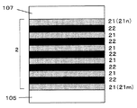
図1は本実施例1に係るLEDを作製するために用いた積層構造体の断面構造を模式的に示す図、図2は図1の積層構造体の発光層の構成を模式的に示す図、図3は図1の積層構造体から作製したLEDの平面構造を模式的に示す図である。 FIG. 1 is a diagram schematically showing a cross-sectional structure of a multilayer structure used for manufacturing an LED according to Example 1, and FIG. 2 is a diagram schematically showing a configuration of a light emitting layer of the multilayer structure in FIG. FIG. 3 is a diagram schematically showing a planar structure of an LED manufactured from the laminated structure of FIG.
LED10を作製するための積層構造体11を形成するために、先ずサファイア基板101を、高周波(RF)誘導加熱用のRFコイルを外周に配置した石英製のMOCVD反応炉内に載置した。窒素ガスを10分間に亘って流通し、反応炉内をパージした後、10分を掛けて基板101の温度を室温から1150℃に昇温した。基板101の温度を1150℃に保ったまま、水素ガスと窒素ガスを流通させながら10分間放置して、基板101の表面をサーマルクリーニングした。
In order to form the
サファイア基板101には、第1の工程として、モル比にして1:2で混合したトリメチルアルミニウム(TMAl)の蒸気とトリメチルガリウム(TMGa)の蒸気とを含む気体と、アンモニア(NH3)とを吹き付ける表面処理を施した。第1の工程での、所謂、V/III比(NH3/(TMAl+TMGa)濃度比率)は約85に設定した。1150℃で6分間、表面処理を施した後、TMGaとTMAlの蒸気を含む気体の反応炉内への供給を停止した。
As a first step, the
続いて、第2の工程としてTMGaとアンモニアガスを流通して、(0001)−サファイア基板101上に、アンドープでn型窒化ガリウム(GaN)層102の形成を1時間掛けて行い、膜厚を0.8μmとした。
Subsequently, TMGa and ammonia gas are circulated as a second step, and an undoped n-type gallium nitride (GaN)
アンドープでn型のGaN層102上には、Siドープn型GaN層103を形成した。同層103の形成時には、シランガス(SiH4)をドーピング源として、電子濃度が5×1018cm-3となる様に珪素(Si)をドーピングした。Siドープn型GaN層103の層厚は2μmとした。
A Si-doped n-
次に、Siドープn型GaN層103上には、TMGaとTMAl、及びNH3を原料とし、SiH4をドーピング源として、Siドープのn型窒化アルミニウム・ガリウム(Al0.09Ga0.91N)層104を形成した。Al0.09Ga0.91N層のキャリア(正孔)濃度は、7×1017cm-3とし、層厚は8nmとした。
Next, on the Si-doped n-
その後、アンモニアガスを反応炉内に流通させながら、基板101の温度を1150℃から830℃へ低下させた。次に、トリメチルインジウム(TMIn)をインジウム原料として、Al0.09Ga0.91N層104上に、膜厚を50nmとするSiドープの窒化ガリウム・インジウム(In0.01Ga0.99N)からなるn型クラッド層105を形成した。
Thereafter, the temperature of the
n型クラッド層105上には、GaNよりなる障壁層21と、In0.04Ga0.96Nよりなる井戸層22で構成される多重量子井戸構造の発光層2を形成した。この多重量子井戸構造の形成にあたっては、SiドープIn0.01Ga0.99Nからなるn型クラッド層105上に、始めにSiドープGaN障壁層21mを形成し、そのSiドープGaN障壁層21m上にIn0.04Ga0.96N井戸層22を形成した。井戸層22の層厚は、全ての井戸層につき、2nmとした。SiドープGaN障壁層21及びIn0.04Ga0.96N井戸層22を交互に5回繰り返し積層したのち、表面に在る5番目のIn0.04Ga0.96N井戸層22上に、改めて、SiドープGaN障壁層21を接合させて設け、多重量子井戸構造の一端層21m及びp型クラッド層107側の他端層21nの両層をSiドープGaN障壁層21とする構造とした。
On the n-
上記のSiドープGaN障壁層21は全部で6層であるが、他端層21nを除く5層のSiドープGaN障壁層21の層厚は15nmとした。一方、他端層21nをなすSiドープGaN障壁層21の層厚は他の障壁層より厚い20nmとした。
The total number of Si-doped GaN barrier layers 21 is six, but the thickness of the five Si-doped GaN barrier layers 21 excluding the
多重量子井戸構造の発光層2上には、マグネシウム(Mg)ドープのAl0.07Ga0.93Nからなるp型クラッド層107を1100℃で形成した。p型クラッド層107のキャリア(正孔)濃度は、5×1017cm-3とし、層厚は10nmとした。
A p-
更に、p型クラッド層107上には、MgドープGaN層をp型コンタクト層108として成長させた。p型コンタクト層108のキャリア(正孔)濃度は8×1017cm-3とし、層厚は100nmとした。
Further, an Mg-doped GaN layer was grown as a p-
p型コンタクト層108の成長を終了した後、誘導加熱式ヒータへの通電を停止して、基板101の温度を室温まで20分を掛けて降温した。成長温度(1100℃)から300℃迄、降温する際には、反応炉内のキャリアガスを窒素とし、併せて容量比率にして1%のNH3を流通した。その後、基板101の温度が300℃となった時点で、NH3の流通を停止し、雰囲気ガスを窒素のみとした。基板101の温度が室温まで降温したのを確認して、積層構造体11を反応炉より外部へ取り出した。
After the growth of the p-
以上の様な降温、冷却操作に依れば、p型コンタクト層108は、p型不純物としてドーピングしたMgを電気的に活性化するためのアニール処理を行わなくても、p型の伝導性を示した。
According to the temperature lowering and cooling operations as described above, the p-
上記の如く形成した積層構造体11に、一般的な選択パターニング技術を応用して選択エッチングを及ぼし、n型オーミック電極109を形成する予定の領域に限り、SiドープGaN層103の表面を露出させた。露出させたSiドープGaN層103の表面には、その表面に接触する側をニッケル(Ni)とした、Ni/アルミニウム(Al)/チタン(Ti)/金(Au)の4層を順次、重層させたn型オーミック電極109を設けた。また、積層構造体11の表面に残置したp型コンタクト層108上の略全面には、図3に示す如く、金(Au)のみからなる透光性のp型オーミック電極110を形成した。p型オーミック電極110上には、下面側から順にチタン(Ti)、アルミニウム(Al)、及び金(Au)を順次積層した構造のボンディングパッド(台座電極)111を接合させて設けた。
The
その後、サファイア基板101の裏面を、当初の350μmから100μm迄、研削し薄板とし、更に、精密に研磨して研削した表面を鏡面状の平坦面に仕上げた。然る後、350μm角の平面視で正方形の個別のLEDチップに切断した。チップ化したLED10を、n型オーミック電極109とp型台座電極111を介して素子駆動電流をLEDチップ10に通流できる様にリードフレームへ接合させた。
Thereafter, the back surface of the
n型オーミック電極109及びp型オーミック電極110間に順方向に素子駆動電流を流してLEDチップ10を発光させた。順方向電流を電流20mAとした際の発光波長は395nmであった。また、一般的な積分球を利用して測定される発光の出力は、8.7mWと高値となった。一方で、順方向電流を20mAとした際の順方向電圧は3.3Vと低値であった。これより、順方向電圧が低く、且つ高発光出力の近紫外LEDがもたらされることが示された。
The
(比較例) 本比較例では、障壁層の層厚を何れも同一とする多重量子井戸構造の発光層を用いてLEDを構成し、発光特性を比較した。 (Comparative example) In this comparative example, LED was comprised using the light emitting layer of the multiple quantum well structure which made the same layer thickness of a barrier layer, and the light emission characteristic was compared.
即ち、上記の実施例1に記載した多重量子井戸構造にあって、他端層(図2の符号21n)をも、他の障壁層と層厚を同一とするSiドープGaN障壁層から構成した。多重量子井戸構造の発光層以外は、実施例1に記載の積層構成、及び電極構成と全く同一とした。
That is, in the multiple quantum well structure described in the first embodiment, the other end layer (
実施例1と同じ方法でマウントしたLEDチップに、リードフレームを介して20mAの順方向電流を流したところ、波長を395nmとする近紫外帯光が出射された。ところが、発光波長は上記の実施例1のLEDチップ10と同一であるものの、順方向電圧は3.5Vとより高くなった。併せて、発光出力値は5.9mWに低下し、実施例1のLED10の特性に及ぶものとは成り得なかった。
(実施例2)
When a forward current of 20 mA was passed through the LED chip mounted by the same method as in Example 1 through a lead frame, near-ultraviolet light having a wavelength of 395 nm was emitted. However, although the emission wavelength is the same as that of the
(Example 2)
本実施例2では、層厚を互いに異にする障壁層を備えた多重量子井戸構造の発光層を利用してIII族窒化物LEDを構成する場合を例にして、本発明の内容を具体的に説明する。 In the second embodiment, the contents of the present invention are specifically described by taking as an example a case where a group III nitride LED is configured using a light emitting layer having a multiple quantum well structure having barrier layers having different layer thicknesses. Explained.
本実施例2では、上記の実施例1に記載の発光層をなす多重量子井戸構造を形成するのにあたり、一端層(図2の符号21m)の障壁層の層厚を15nmとし、2番目の障壁層の層厚を16nmとし、3番目の障壁層の層厚を17nmとし、4番目の障壁層の層厚を18nmとし、5番目の障壁層の層厚を19nmとした。 In Example 2, when forming the multiple quantum well structure forming the light emitting layer described in Example 1, the thickness of the barrier layer of one end layer (reference numeral 21m in FIG. 2) is set to 15 nm. The thickness of the barrier layer was 16 nm, the thickness of the third barrier layer was 17 nm, the thickness of the fourth barrier layer was 18 nm, and the thickness of the fifth barrier layer was 19 nm.
即ち、n型クラッド層(図1、図2の符号105)からp型クラッド層(図1、図2の符号107)に向けて、SiドープGaN障壁層の層厚を、順次厚くして、量子井戸構造を構成した。他端層21nをなすSiドープGaN障壁層の層厚は20nmとした。
That is, from the n-type cladding layer (
上記の実施例1と同一の方法で作製したLEDチップに、順方向に20mAの素子駆動電流を通流させて特性を評価した。発光波長は395nmであった。順方向電圧は3.3Vと高くなったものの、発光出力は実施例1と同様に8.9mWと高く、高出力の近紫外LEDがもたらされ、比較例に記載の従来のLEDに比べれば、順方向電圧、及び発光出力に優れるLEDとなった。 The characteristics were evaluated by passing an element drive current of 20 mA in the forward direction through the LED chip produced by the same method as in Example 1 above. The emission wavelength was 395 nm. Although the forward voltage was as high as 3.3 V, the light output was as high as 8.9 mW as in Example 1, resulting in a high-power near-ultraviolet LED, compared to the conventional LED described in the comparative example. The LED has excellent forward voltage and light output.
(実施例3) 他端層に、不純物濃度に分布を付した障壁層を用いた多重量子井戸構造の発光層を利用してIII族窒化物半導体層を構成する場合を例にして、本発明を具体的に説明する。 (Example 3) In the case where a group III nitride semiconductor layer is formed using a light emitting layer having a multiple quantum well structure using a barrier layer having a distribution of impurity concentration at the other end layer, the present invention is taken as an example. Will be described in detail.
本実施例3では、上記の実施例1に記載の多重量子井戸構造をなす他端層21nを、Si不純物の濃度を、井戸層と接合する領域側で低くし、層の中央部でより高くし、中央部より層厚の増加方向(p型クラッド層107の方向)に向けて漸次減少させたSiドープGaN層から構成した。
In the third embodiment, the
他端層では、井戸層との接合界面から、層厚の増加方向に5nmに至る内部領域において、Si不純物の濃度は3×1017cm-3とした。井戸層との接合界面から層厚方向に5nmを超え、10nmに至る障壁層の中央の領域でのSi不純物の濃度は、4×1018cm-3とした。また、中央の領域からp型クラッド層との接合界面に向けた領域では、Si不純物の濃度を4×1018cm-3から、7×1017cm-3へ直線的に減少させた。各領域のSi不純物濃度は、他端層をなす障壁層の成長時に、反応系へ供給するSiH4ガスの流量を経時的に変化させて調整した。 In the other end layer, the Si impurity concentration was set to 3 × 10 17 cm −3 in the inner region extending from the junction interface with the well layer to 5 nm in the increasing direction of the layer thickness. The concentration of the Si impurity in the central region of the barrier layer exceeding 5 nm in the layer thickness direction from the junction interface with the well layer and reaching 10 nm was 4 × 10 18 cm −3 . In the region from the central region toward the junction interface with the p-type cladding layer, the Si impurity concentration was linearly decreased from 4 × 10 18 cm −3 to 7 × 10 17 cm −3 . The Si impurity concentration in each region was adjusted by changing the flow rate of the SiH 4 gas supplied to the reaction system over time during the growth of the barrier layer forming the other end layer.
実施例1と同じ方法でLEDチップを作製し、チップに順方向電流を流したところ、順方向電流を20mAとした際の発光波長は395nmであった。また、順方向電圧は3.2Vと低く、発光の出力は8.6mWであり、比較例に記載の従来のLEDに比べれば、順方向電圧、及び発光出力に優れるLEDとなった。 When an LED chip was produced by the same method as in Example 1 and a forward current was passed through the chip, the emission wavelength when the forward current was 20 mA was 395 nm. Further, the forward voltage was as low as 3.2 V, and the light emission output was 8.6 mW, which was an LED superior in forward voltage and light emission output as compared with the conventional LED described in the comparative example.
2 発光層
10 LED
11 積層構造体
21 障壁層
21m 一端層(障壁層)
21n 他端層(障壁層)
22 井戸層
101 結晶基板
102 アンドープn型GaN層
103 Siドープn型GaN層
104 Siドープn型窒化アルミニウム・ガリウム(Al0.09Ga0.91N)層
105 n型クラッド層
106 発光層
107 p型クラッド層
108 p型コンタクト層
109 n型オーミック電極
110 p型オーミック電極
111 ボンディングパッド(台座電極)
2
11
21n other end layer (barrier layer)
22
Claims (4)
上記発光層は、n型クラッド層に最も近接して対峙する一端層、及びp型クラッド層に最も近接して対峙する他端層とが共に障壁層であり、その他端層は他の障壁層よりも層厚が大である、
ことを特徴とするpn接合型III族窒化物半導体発光素子。 A well layer and a barrier layer made of a group III nitride semiconductor are alternately stacked over several cycles between an n-type cladding layer made of a group III nitride semiconductor and a p-type cladding layer formed on a crystal substrate. In a pn junction type III-nitride semiconductor light emitting device having a light emitting layer having a multiple quantum well structure,
In the light emitting layer, one end layer facing closest to the n-type cladding layer and the other end layer facing closest to the p-type cladding layer are both barrier layers, and the other end layer is another barrier layer. The layer thickness is greater than
A pn junction group III nitride semiconductor light emitting device characterized by the above.
Priority Applications (1)
| Application Number | Priority Date | Filing Date | Title |
|---|---|---|---|
| JP2005061867A JP2005294813A (en) | 2004-03-08 | 2005-03-07 | Pn junction type group iii nitride semiconductor light-emitting device |
Applications Claiming Priority (2)
| Application Number | Priority Date | Filing Date | Title |
|---|---|---|---|
| JP2004063946 | 2004-03-08 | ||
| JP2005061867A JP2005294813A (en) | 2004-03-08 | 2005-03-07 | Pn junction type group iii nitride semiconductor light-emitting device |
Publications (1)
| Publication Number | Publication Date |
|---|---|
| JP2005294813A true JP2005294813A (en) | 2005-10-20 |
Family
ID=35327349
Family Applications (1)
| Application Number | Title | Priority Date | Filing Date |
|---|---|---|---|
| JP2005061867A Pending JP2005294813A (en) | 2004-03-08 | 2005-03-07 | Pn junction type group iii nitride semiconductor light-emitting device |
Country Status (1)
| Country | Link |
|---|---|
| JP (1) | JP2005294813A (en) |
Cited By (4)
| Publication number | Priority date | Publication date | Assignee | Title |
|---|---|---|---|---|
| US8168966B2 (en) | 2005-09-13 | 2012-05-01 | Sony Corporation | GaN-based semiconductor light-emitting device, light illuminator, image display planar light source device, and liquid crystal display assembly |
| JP2018152458A (en) * | 2017-03-13 | 2018-09-27 | 住友電気工業株式会社 | Light-emitting diode |
| CN111180559A (en) * | 2018-11-12 | 2020-05-19 | 晶元光电股份有限公司 | semiconductor element |
| DE102008064974B4 (en) * | 2007-12-18 | 2025-10-09 | Seoul Viosys Co., Ltd. | Light-emitting diode with an active region made of a multiple-quantum well structure |
Citations (5)
| Publication number | Priority date | Publication date | Assignee | Title |
|---|---|---|---|---|
| JP2000332364A (en) * | 1999-05-17 | 2000-11-30 | Matsushita Electric Ind Co Ltd | Nitride semiconductor device |
| JP2000349337A (en) * | 1999-06-07 | 2000-12-15 | Nichia Chem Ind Ltd | Nitride semiconductor device |
| JP2001102629A (en) * | 1999-09-28 | 2001-04-13 | Nichia Chem Ind Ltd | Nitride semiconductor device |
| JP2002223042A (en) * | 2000-11-21 | 2002-08-09 | Nichia Chem Ind Ltd | Nitride semiconductor device |
| JP2003031902A (en) * | 2001-07-16 | 2003-01-31 | Denso Corp | Semiconductor laser |
-
2005
- 2005-03-07 JP JP2005061867A patent/JP2005294813A/en active Pending
Patent Citations (5)
| Publication number | Priority date | Publication date | Assignee | Title |
|---|---|---|---|---|
| JP2000332364A (en) * | 1999-05-17 | 2000-11-30 | Matsushita Electric Ind Co Ltd | Nitride semiconductor device |
| JP2000349337A (en) * | 1999-06-07 | 2000-12-15 | Nichia Chem Ind Ltd | Nitride semiconductor device |
| JP2001102629A (en) * | 1999-09-28 | 2001-04-13 | Nichia Chem Ind Ltd | Nitride semiconductor device |
| JP2002223042A (en) * | 2000-11-21 | 2002-08-09 | Nichia Chem Ind Ltd | Nitride semiconductor device |
| JP2003031902A (en) * | 2001-07-16 | 2003-01-31 | Denso Corp | Semiconductor laser |
Cited By (5)
| Publication number | Priority date | Publication date | Assignee | Title |
|---|---|---|---|---|
| US8168966B2 (en) | 2005-09-13 | 2012-05-01 | Sony Corporation | GaN-based semiconductor light-emitting device, light illuminator, image display planar light source device, and liquid crystal display assembly |
| DE102008064974B4 (en) * | 2007-12-18 | 2025-10-09 | Seoul Viosys Co., Ltd. | Light-emitting diode with an active region made of a multiple-quantum well structure |
| JP2018152458A (en) * | 2017-03-13 | 2018-09-27 | 住友電気工業株式会社 | Light-emitting diode |
| CN111180559A (en) * | 2018-11-12 | 2020-05-19 | 晶元光电股份有限公司 | semiconductor element |
| CN111180559B (en) * | 2018-11-12 | 2023-11-28 | 晶元光电股份有限公司 | Semiconductor components |
Similar Documents
| Publication | Publication Date | Title |
|---|---|---|
| CN101689586B (en) | Nitride semiconductor light emitting element and method for manufacturing nitride semiconductor | |
| CN100547814C (en) | N-type group III nitride semiconductor stacked structure | |
| US20050277218A1 (en) | Group III nitride compound semiconductor light-emitting device and method for producing the same | |
| TW200402896A (en) | Semiconductor light-emitting device | |
| JPWO2006038665A1 (en) | Nitride semiconductor light emitting device and manufacturing method thereof | |
| JP2013115105A (en) | Nitride semiconductor light-emitting element and nitride semiconductor light-emitting element manufacturing method | |
| JP2005244207A (en) | Gallium nitride compound semiconductor light emitting device | |
| CN101180743A (en) | Nitride semiconductor light emitting element | |
| US7781777B2 (en) | Pn junction type group III nitride semiconductor light-emitting device | |
| JP3233139B2 (en) | Nitride semiconductor light emitting device and method of manufacturing the same | |
| JP3567926B2 (en) | pn junction type boron phosphide-based semiconductor light emitting device, method for manufacturing the same, and light source for display device | |
| JP2008130877A (en) | Manufacturing method of nitride semiconductor light emitting device | |
| TWI270220B (en) | Group III nitride semiconductor light emitting device | |
| JP2008130878A (en) | Nitride semiconductor light emitting device | |
| JP3724267B2 (en) | Group III nitride semiconductor light emitting device | |
| JP2008078297A (en) | GaN-based semiconductor light emitting device | |
| JP4827706B2 (en) | Nitride semiconductor light emitting device | |
| JP2005294813A (en) | Pn junction type group iii nitride semiconductor light-emitting device | |
| JP4781028B2 (en) | Group III nitride semiconductor laminate and method for manufacturing group III nitride semiconductor light emitting device | |
| JP2006013463A (en) | Group iii nitride semiconductor light emitting element | |
| US8354687B1 (en) | Efficient thermal management and packaging for group III nitride based UV devices | |
| JP2005340762A (en) | Group iii nitride semiconductor light-emitting element | |
| JP2003142730A (en) | Semiconductor light emitting element | |
| TWI255053B (en) | Pn junction type group III nitride semiconductor light-emitting device | |
| JP2010232290A (en) | Nitride semiconductor light emitting diode and manufacturing method thereof |
Legal Events
| Date | Code | Title | Description |
|---|---|---|---|
| A621 | Written request for application examination |
Free format text: JAPANESE INTERMEDIATE CODE: A621 Effective date: 20080107 |
|
| A131 | Notification of reasons for refusal |
Free format text: JAPANESE INTERMEDIATE CODE: A131 Effective date: 20100608 |
|
| A977 | Report on retrieval |
Free format text: JAPANESE INTERMEDIATE CODE: A971007 Effective date: 20100608 |
|
| A521 | Written amendment |
Free format text: JAPANESE INTERMEDIATE CODE: A523 Effective date: 20100809 |
|
| A131 | Notification of reasons for refusal |
Free format text: JAPANESE INTERMEDIATE CODE: A131 Effective date: 20101026 |
|
| A02 | Decision of refusal |
Free format text: JAPANESE INTERMEDIATE CODE: A02 Effective date: 20110308 |