JP2005294807A - Method for manufacturing photoelectric conversion device - Google Patents
Method for manufacturing photoelectric conversion device Download PDFInfo
- Publication number
- JP2005294807A JP2005294807A JP2005037097A JP2005037097A JP2005294807A JP 2005294807 A JP2005294807 A JP 2005294807A JP 2005037097 A JP2005037097 A JP 2005037097A JP 2005037097 A JP2005037097 A JP 2005037097A JP 2005294807 A JP2005294807 A JP 2005294807A
- Authority
- JP
- Japan
- Prior art keywords
- photoelectric conversion
- resin substrate
- substrate
- adhesion layer
- manufacturing
- Prior art date
- Legal status (The legal status is an assumption and is not a legal conclusion. Google has not performed a legal analysis and makes no representation as to the accuracy of the status listed.)
- Granted
Links
Images
Classifications
-
- Y—GENERAL TAGGING OF NEW TECHNOLOGICAL DEVELOPMENTS; GENERAL TAGGING OF CROSS-SECTIONAL TECHNOLOGIES SPANNING OVER SEVERAL SECTIONS OF THE IPC; TECHNICAL SUBJECTS COVERED BY FORMER USPC CROSS-REFERENCE ART COLLECTIONS [XRACs] AND DIGESTS
- Y02—TECHNOLOGIES OR APPLICATIONS FOR MITIGATION OR ADAPTATION AGAINST CLIMATE CHANGE
- Y02E—REDUCTION OF GREENHOUSE GAS [GHG] EMISSIONS, RELATED TO ENERGY GENERATION, TRANSMISSION OR DISTRIBUTION
- Y02E10/00—Energy generation through renewable energy sources
- Y02E10/50—Photovoltaic [PV] energy
Landscapes
- Photovoltaic Devices (AREA)
Abstract
【課題】より光電変換効率を高く、簡便に形成できる光電変換装置の製造方法を提供すること。
【解決手段】支持基板上に樹脂基板を固着させた後に光電変換素子を形成する光電変換装置の製造方法において、硬化後に所定の軟性を持ち、かつ未硬化状態で表面を平滑とした密着層を支持基板に形成した後に、この密着層を完全に硬化させる工程と、支持基板上に密着層を介して樹脂基板を貼り付ける工程と、密着層と樹脂基板との界面に存在する気泡を除去するための脱気処理をして、密着層と樹脂基板とを真空吸着する工程と、樹脂基板上に光電変換素子を形成する工程と、支持基板と樹脂基板とを分離する工程を有する製造方法を採用した。
【選択図】 図1
The present invention provides a method for manufacturing a photoelectric conversion device that has higher photoelectric conversion efficiency and can be easily formed.
In a method for manufacturing a photoelectric conversion device in which a photoelectric conversion element is formed after fixing a resin substrate on a support substrate, an adhesion layer having a predetermined softness after curing and having a smooth surface in an uncured state is provided. After the formation on the support substrate, the step of completely curing the adhesion layer, the step of attaching the resin substrate on the support substrate via the adhesion layer, and the bubbles present at the interface between the adhesion layer and the resin substrate are removed. And a manufacturing method including a step of vacuum adsorbing the adhesion layer and the resin substrate, a step of forming a photoelectric conversion element on the resin substrate, and a step of separating the support substrate and the resin substrate. Adopted.
[Selection] Figure 1
Description
本発明は、支持基板上に樹脂基板を固着させた後に光電変換層を形成する光電変換装置の製造方法に関する。 The present invention relates to a method for manufacturing a photoelectric conversion device in which a photoelectric conversion layer is formed after a resin substrate is fixed on a support substrate.
アモルファスシリコン膜からなる光電変換層が樹脂基板上に形成された光電変換装置は、ガラス基板や金属基板を用いて形成されたものに比べて、軽量、薄型であるうえに可撓性を有している点に優れており、この特性を生かして、腕時計などの小型携帯機器に使用されている。 A photoelectric conversion device in which a photoelectric conversion layer made of an amorphous silicon film is formed on a resin substrate is lighter and thinner and more flexible than those formed using a glass substrate or a metal substrate. It is used for small portable devices such as wristwatches by taking advantage of this characteristic.
この様な光電変換装置は、装置を構成する光電変換層、その光電変換層を挟持する透明電極層、裏面電極層を有するため、各層を加熱処理をしながら形成しなくてはならない。したがって、下記に示す製造方法が提案された(例えば、特許文献1参照)。
なお、本手段を第1の手段とする。
Since such a photoelectric conversion device includes a photoelectric conversion layer constituting the device, a transparent electrode layer sandwiching the photoelectric conversion layer, and a back electrode layer, each layer must be formed while heat treatment. Therefore, the manufacturing method shown below was proposed (for example, refer patent document 1).
This means is the first means.
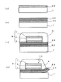
図5は、第1の手段の製造工程を示す図面であり、ガラス等の支持基板1上に樹脂基板21を固定して光電変換素子7を形成した後、支持基板1から樹脂基板21を剥離して光電変換装置9を得る方法を示している。
FIG. 5 is a drawing showing a manufacturing process of the first means. After the
まず図5(a)に示す様に、耐熱性があり、かつ支持基板1との密着強度が弱い樹脂材料(一般にはポリイミド樹脂)を、未硬化のペースト状態(一般にはポリイミドワニスの状態)で支持基板1上に塗布する。その後、この状態の支持基板1を加熱硬化して、支持基板1上に半硬化状態の樹脂基板21を形成する。なお、この段階での樹脂基板21は、完全硬化させてしまうと後で支持基板1から容易に剥離できなくなるので、少なくとも剥離する工程までは、その一連の工程に渡って硬化温度を低くしてポリイミドのイミド化を抑えるように加熱をすることが肝要である。つまり、この状態で樹脂基板21は、半硬化状態となっている。
First, as shown in FIG. 5A, a resin material (generally polyimide resin) that has heat resistance and weak adhesion strength to the
次に図5(b)に示す様に、樹脂基板21上に、酸化インジウムスズ(ITO)等の透明電極層5、アモルファスシリコン膜からなる光電変換層6、TiやAlなどの金属からなる裏面電極層7を順次積層して光電変換素子8を形成する。その後、光電変換素子8の表面を保護膜9で被覆する。
Next, as shown in FIG. 5B, on the
光電変換層6となるアモルファスシリコン膜の形成には、概してプラズマCVD法が用いられ、CVD装置内に生成したプラズマにより原料ガスを分解し、P型、I型、N型の順にアモルファスシリコン膜を積層する。P型アモルファスシリコン膜はシラン(SiH
4)ガスとジボラン(B2H6)ガスを、I型アモルファスシリコン膜はSiH4ガスを、N型アモルファスシリコン膜はSiH4ガスとホスフィン(PH3)ガスを原料ガスとして装置内に導入して形成する。そして、この成膜工程において良質のアモルファスシリコン膜を形成するためには、CVD装置内で基板温度を150℃以上にして成膜することが必須となる。
For the formation of the amorphous silicon film to be the
4 ) Gas and diborane (B 2 H 6 ) gas, SiH 4 gas for the I-type amorphous silicon film, and SiH 4 gas and phosphine (PH 3 ) gas for the N-type amorphous silicon film are introduced into the apparatus. Form. In order to form a high-quality amorphous silicon film in this film forming process, it is essential to form the film at a substrate temperature of 150 ° C. or higher in the CVD apparatus.
最後に、支持基板1を水中に浸漬する。すると樹脂基板21は十分に硬化していないので吸水し、支持基板1と樹脂基板21の密着力が低下する。すると、図5(c)示すように両基板の界面を境として支持基板1と樹脂基板21とが剥離して、樹脂基板21上に光電変換素子8を有する、目的の光電変換装置10が得られる。
Finally, the
また、上記第1に手段に類似する、光電変換装置10の他の製造方法も提案されている(例えば、特許文献2参照)。この製造方法を、図6に基づき説明をする。なお、本手段を第2の手段とする。
初めに図6(a)に示す様に、ポリイミド樹脂を、未硬化のペースト状態で支持基板1上に10〜15μm程の厚さで塗布して剥離樹脂層22を形成する。この剥離樹脂層22には、ポリイミドの前駆体であるポリアミック酸溶液を使用し、スクリーン印刷法を用いて塗布する。
Further, another method for manufacturing the
First, as shown in FIG. 6A, a polyimide resin is applied on the
次に図6(b)に示す様に、この剥離樹脂層22が未硬化のまま(半硬化のまま)、樹脂基板23を積層して、ラミネート装置を利用して熱圧着する。こうして剥離樹脂層22を介して樹脂基板23を支持基板1に接着する。ここで、樹脂基板23にはポリイミドフィルムを使用し、必要に応じて350℃の熱風乾燥炉を使用して剥離樹脂層22を仮硬化させても良い。その際は、ポリアミック酸溶液は350℃以上で重合してポリイミドとなるから、これよりも50〜100℃程度硬化温度を低くして仮硬化させ、最終的に行われる剥離樹脂層22の支持基板1からの剥離性を向上させることが必要である。
Next, as shown in FIG. 6B, the
更に、図6(c)に示す様に、樹脂基板23の上に透明電極層5、アモルファスシリコン膜からなる光電変換層6、裏面電極層7を第1の手段と同様に順次積層して、光電変換素子8を形成する。そして、この光電変換素子8の表面を保護膜9で被覆する。
Further, as shown in FIG. 6C, the
この後、支持基板1を水中に浸漬したまま約1時間放置すると、自然に剥離樹脂層3aを境界として、図6(d)に示すように支持基板1と樹脂基板23とが遊離し、目的の光電変換装置10が完成する。
Thereafter, when the
この第2の手段においては、樹脂基板23が剥離後の光電変換装置10の基板となるから、剥離樹脂層22は、樹脂基板23と強い密着強度は必要なく、剥離性のみを重視して形成できるという利点を有している。
In this second means, since the
さらに、剥離樹脂層22の厚さは、第1の手段の樹脂基板21(図5参照)の1/10程度に薄く形成できるので、剥離樹脂層22が例え半硬化の状態であっても、アモルファスシリコン膜を形成する際に剥離樹脂層22から発生するアウトガスを微量とすることができる。
Furthermore, since the thickness of the
しかしながら、前述した第1の手段、第2の手段には、それぞれ下記に示す問題点を有している。
第1の手段における樹脂基板21は、光電変換装置10としての強度を保持する必要があるために、10〜20μmの厚みが要求される。一般にポリイミドワニスは、硬化する時に膜厚が1/10程度となってしまうため、支持基板1上に未硬化のペーストの樹脂を塗布する工程で、予めその分の厚み減少を考慮して、ポリイミドワニスを100〜200μm塗布する必要がある。しかしながら、これだけの厚みのポリイミドワニスは、一般的に膜を簡易的に塗る手段として多用されているスクリーン印刷等の方法で塗布することが難しい。
However, the first means and the second means described above have the following problems.
The
また、光電変換層6となるアモルファスシリコン膜を形成する際には、前述した様にCVD装置内において150℃以上に基板を加熱しながら成膜を行う必要がある。この段階
では、樹脂基板21が十分に硬化していないので、樹脂基板21からアウトガスが放出してしまう。このアウトガスは、半硬化状態の樹脂基板21の吸水率が大きいこと、ポリイミドワニスの残存溶媒の発生、半硬化状態の樹脂基板21の残留未反応部が脱水重合反応することにより発生する水分、などに起因して発生するものである。
Further, when the amorphous silicon film to be the
なお、アモルファスシリコン膜の成膜時には、原料ガスとして、SiH4ガスをベースにB2H6ガスやPH3ガスを導入して膜への不純物ドーピングを行い、電気伝導度と伝導型(PまたはN)が最適になるよう制御している。従って、硬化不十分な樹脂基板21から発生するアウトガスは、光電変換層6の成膜段階で不純物としてアモルファスシリコン膜中に取り込まれ、これが光電変換層6の膜質を低下させる原因となる。
When the amorphous silicon film is formed, B 2 H 6 gas or PH 3 gas is introduced as a source gas based on SiH 4 gas to dope impurities into the film, and the electric conductivity and conductivity type (P or N) is controlled to be optimum. Therefore, the outgas generated from the
また、樹脂基板21と支持基板1との剥離工程において、半硬化状態の樹脂基板21は、吸水性および水分の透過性が大きくなり、これにより光電変換装置10自体の信頼性を低下させてしまう。
Moreover, in the peeling process of the
この様に第1の手段は、樹脂基板21の剥離性と、製造される装置の信頼性を両立させることが難しい製造方法であることは明らかである。
Thus, it is obvious that the first means is a manufacturing method in which it is difficult to achieve both the peelability of the
また、第2の手段におけるポリイミドフィルムからなる樹脂基板23と支持基板1との接着は、半硬化状態の剥離樹脂層22を介して行っている。そして、剥離樹脂層22を支持基板1との剥離性を重視して形成すると、樹脂基板23と剥離樹脂層21とを確実に接着させることはできない。
Further, the adhesion between the
この様に、樹脂基板23と支持基板1との十分な接着強度が得られない状態で、光電変換層6となるアモルファスシリコン膜を150℃以上で成膜すると、樹脂基板23と支持基板1の熱膨張係数の違いから、樹脂基板23が支持基板1から部分的に分離してしまうことになり、その箇所に形成されるアモルファスシリコン膜は、加熱されないこととなる。すると、この箇所の膜質は、他の膜質と異なったものとなってしまう。
As described above, when an amorphous silicon film serving as the
また、この手段では、第1の手段と同様に微量なアウトガスが依然として発生しているため、やはりこのアウトガスがアモルファスシリコン膜に及ぼす膜質への悪影響を完全に解消することはできない。 In addition, in this means, since a very small amount of outgas is still generated as in the first means, it is still impossible to completely eliminate the adverse effect of the outgas on the amorphous silicon film on the film quality.
さらに、樹脂基板23を支持基板1から剥離するためには、自然に剥離するまで水中に浸漬しておかなければならず、剥離工程に時間が掛かる。そして、この剥離工程の後はさらに乾燥工程が必要になり、全工程に掛かる時間が冗長となってしまう。
Furthermore, in order to peel the
そこで、本発明の目的は上記課題を解決し、より光電変換効率を高く、簡便に形成できる光電変換装置の製造方法を提供することである。 Accordingly, an object of the present invention is to solve the above-described problems and provide a method for manufacturing a photoelectric conversion device that can be easily formed with higher photoelectric conversion efficiency.
本発明の光電変換装置の製造方法は、上記した目的を達成するため、基本的には、以下に記載された製造方法を採用するものである。 In order to achieve the above-described object, the photoelectric conversion device manufacturing method of the present invention basically employs the manufacturing method described below.
即ち、本発明の光電変換装置の製造方法は、支持基板上に樹脂基板を固着させた後に光電変換素子を形成する光電変換装置の製造方法において、硬化後に所定の軟性を持ち、かつ未硬化状態で表面を平滑とした密着層を支持基板に形成した後に、この密着層を完全に硬化させる工程と、支持基板上に密着層を介して樹脂基板を貼り付ける工程と、密着層と樹脂基板との界面に存在する気泡を除去するための脱気処理をして、密着層と樹脂基板とを真空吸着する工程と、樹脂基板上に光電変換素子を形成する工程と、支持基板と樹脂基
板とを分離する工程とを含むことを特徴とするものである。
That is, the method for manufacturing a photoelectric conversion device of the present invention is a method for manufacturing a photoelectric conversion device in which a photoelectric conversion element is formed after fixing a resin substrate on a support substrate, has a predetermined flexibility after curing, and is in an uncured state. And forming the adhesion layer with a smooth surface on the support substrate, then completely curing the adhesion layer, attaching the resin substrate on the support substrate via the adhesion layer, the adhesion layer and the resin substrate, Performing a deaeration process to remove bubbles present at the interface of the substrate, vacuum-adsorbing the adhesion layer and the resin substrate, forming a photoelectric conversion element on the resin substrate, a support substrate and a resin substrate, And a step of separating.
また、本発明の光電変換装置の製造方法は、前述した脱気処理を、真空中で行うことを特徴とするものである。 The method for manufacturing a photoelectric conversion device according to the present invention is characterized in that the above-described deaeration treatment is performed in a vacuum.
さらに、本発明の光電変換装置の製造方法は、前述した脱気処理を、真空中で加熱して行うことを特徴とするものである。 Furthermore, the method for manufacturing a photoelectric conversion device of the present invention is characterized in that the above-described deaeration treatment is performed by heating in vacuum.
またさらに、本発明の光電変換装置の製造方法は、支持基板と樹脂基板とを分離する工程が、樹脂基板端部に粘着テープを貼り付けて、その粘着テープを支点として支持基板と樹脂基板とを分離する工程であることを特徴とするものである。 Furthermore, in the method for manufacturing a photoelectric conversion device according to the present invention, the step of separating the support substrate and the resin substrate includes attaching an adhesive tape to the end of the resin substrate, and using the adhesive tape as a fulcrum, It is the process of isolate | separating.
またさらに、本発明の光電変換装置の製造方法は、前述した光電変換素子を形成する工程の前に、樹脂基板の内部応力を緩和するための予備加熱処理を行うことを特徴とするものである。 Furthermore, the method for manufacturing a photoelectric conversion device according to the present invention is characterized in that a preheating treatment for relieving internal stress of the resin substrate is performed before the step of forming the photoelectric conversion element described above. .
またさらに、本発明の光電変換装置の製造方法は、前述した予備加熱処理を行う加熱温度が、光電変換素子を形成する工程で行う加熱温度よりも少なくとも高い温度であることを特徴とするものである。 Furthermore, the method for manufacturing a photoelectric conversion device according to the present invention is characterized in that the heating temperature at which the above-described preheating treatment is performed is at least higher than the heating temperature at which the photoelectric conversion element is formed. is there.
またさらに、本発明の光電変換装置の製造方法は、前述した密着層と樹脂基板とを真空吸着する工程にて、予備加熱処理を行うことを特徴とするものである。 Furthermore, the method for manufacturing a photoelectric conversion device of the present invention is characterized in that a preheating treatment is performed in the step of vacuum adsorbing the adhesion layer and the resin substrate described above.
またさらに、本発明の光電変換装置の製造方法は、前述した予備加熱する工程を、150℃、1時間で測定した熱収縮率が前記樹脂基板の全方向で1%以下であり、かつ表面粗さ(Ra)が20nm未満となる条件にて行うことを特徴とするものである。 Furthermore, in the method for producing a photoelectric conversion device of the present invention, the preheating step described above has a heat shrinkage rate of 1% or less in all directions of the resin substrate measured at 150 ° C. for 1 hour, and has a rough surface. (Ra) is performed under the condition of less than 20 nm.
本発明の光電変換装置の製造方法は、樹脂基板と支持基板とを、シリコーンゴムを用いた完全に硬化させた密着層を介して真空吸着により強固に密着させた後に、光電変換層を形成しているので、例え、光電変換素子の製造過程で加熱処理を行った際に、両基板の線膨張係数の違いによる応力がこの樹脂基板に掛かったとしても、樹脂基板が支持基板から分離することを極力防止することができる。 The method for producing a photoelectric conversion device of the present invention comprises forming a photoelectric conversion layer after firmly adhering a resin substrate and a support substrate by vacuum adsorption through a completely cured adhesion layer using silicone rubber. Therefore, even if heat treatment is performed during the manufacturing process of the photoelectric conversion element, even if stress due to the difference in linear expansion coefficient between the two substrates is applied to the resin substrate, the resin substrate must be separated from the support substrate. Can be prevented as much as possible.
さらに、本発明の光電変換装置の製造方法は、前述した完全に硬化させた密着層を用いた工程を採用しているので、特にアモルファスシリコンからなる光電変換素層を形成する工程で加熱処理を施しても、密着層からアウトガスが発生することはなくなり、光電変換素層の膜質の低下を防止することができる。 Furthermore, since the manufacturing method of the photoelectric conversion device of the present invention employs the process using the above-mentioned completely cured adhesion layer, the heat treatment is performed particularly in the process of forming the photoelectric conversion element layer made of amorphous silicon. Even if it applies, outgas does not generate | occur | produce from a contact | adherence layer, and the fall of the film quality of a photoelectric conversion element layer can be prevented.
またさらに、本発明の製造方法を適用すると、樹脂基板と支持基板とが強固に密着することとなるが、樹脂基板の端部に粘着テープを貼り付けて、その粘着テープを支点として樹脂基板の端部から剥がし、密着層と樹脂基板との界面に空気を侵入させれば、樹脂基板を支持基板から容易に分離することができ、この工程における製造時間を大幅に短縮することができる。
この様に、支持基板と樹脂基板の分離が容易なので、この樹脂基板を貼り付ける際には何度でも貼り直しが可能であるという利点も有している。
Furthermore, when the manufacturing method of the present invention is applied, the resin substrate and the support substrate are firmly adhered, but an adhesive tape is attached to the end of the resin substrate, and the adhesive tape is used as a fulcrum for the resin substrate. If it is peeled off from the end and air is allowed to enter the interface between the adhesion layer and the resin substrate, the resin substrate can be easily separated from the support substrate, and the manufacturing time in this step can be greatly shortened.
As described above, since the support substrate and the resin substrate can be easily separated, there is an advantage that the resin substrate can be reattached any number of times.
本発明の光電変換装置の製造方法は、硬化後に所定の軟性を持ち、かつ未硬化状態で表面を平滑とした密着層を支持基板に形成した後に、この密着層を完全に硬化させる工程と
、支持基板上に密着層を介して樹脂基板を貼り付ける工程と、密着層と樹脂基板との界面に存在する気泡を除去するための脱気処理をして、密着層と樹脂基板を真空吸着する工程と、さらに、樹脂基板上に光電変換素子を形成する工程と、支持基板と樹脂基板とを分離する工程とを有することを特徴とする製造方法である。
以下に、本発明の実施の形態を上記に示した工程順に図面に基づいて詳細に説明する。なお、従来技術で使用した同じ部材については、同じ符号を付して説明をする。
The process for producing the photoelectric conversion device of the present invention comprises a step of completely curing the adhesion layer after forming an adhesion layer having a predetermined softness after curing and having a smooth surface in an uncured state on the support substrate; A process of attaching the resin substrate to the support substrate via the adhesion layer and a deaeration process for removing bubbles existing at the interface between the adhesion layer and the resin substrate, and vacuum-adsorbing the adhesion layer and the resin substrate. And a step of forming a photoelectric conversion element on the resin substrate and a step of separating the support substrate and the resin substrate.
Hereinafter, embodiments of the present invention will be described in detail based on the drawings in the order of the steps shown above. In addition, about the same member used by the prior art, the same code | symbol is attached | subjected and demonstrated.
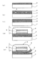
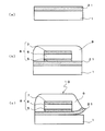
まず、本発明の光電変換装置の製造方法について、図1の工程断面図にしたがって説明をする。図1(a)は、硬化後に所定の軟性を持ち、かつ未硬化状態で表面を平滑とした密着層2を支持基板1に形成した後に、この密着層2を完全に硬化させる工程を示している。
First, the manufacturing method of the photoelectric conversion apparatus of this invention is demonstrated according to process sectional drawing of FIG. FIG. 1A shows a step of completely curing the
先ず、図1(a)に示す様に、ガラス製の支持基板1における一方の面の全面に、硬化後のゴム硬度が20〜50(JIS A)となる液状のシリコーンゴム(例えばジーイー東芝シリコーン社製、製品名:TSE3033)を、スピンコータを使用して50μm程度の厚さに塗布する。
First, as shown in FIG. 1A, a liquid silicone rubber (for example, GE Toshiba Silicone) having a cured rubber hardness of 20 to 50 (JIS A) is formed on the entire surface of one surface of the
その後、200℃に設定したドライオーブンに、この液状のシリコーンゴムが塗布された支持基板1を投入して60分間加熱し、このシリコーンゴムを完全に硬化させ、支持基板1に確実に固着された密着層2を形成する。
Thereafter, the
この際、密着層2の表面は平滑に形成されていることが必要である。この平滑化は、次工程(支持基板上に密着層を介して樹脂基板を貼り付ける工程)において、樹脂基板3と密着層2とを確実に真空吸着させて固定するために必要となる。
At this time, the surface of the
図1(b)は、支持基板1上に密着層2を介して樹脂基板3を貼り付ける工程を示している。
上記のようにして、支持基板1上に密着層2を形成したら、次に、図1(b)に示すように、フィルム状の樹脂基板3を支持基板1上に密着層2を介して貼り付ける。樹脂基板3を支持基板1の端部から徐々に密着層2に貼っていくと、樹脂基板3と密着層2の界面から空気4が徐々に押し出されて、その界面はほぼ真空に近い状態になる。すると、樹脂基板3と密着層2とは密着して、支持基板1に固着される。
FIG. 1B shows a process of attaching the
After the
なお、樹脂基板3を密着層2に貼り付ける際に樹脂基板3を貼り損ねたとしても、樹脂基板3の端部に粘着テープを貼って、この部分を支点にして樹脂基板3を剥がし、再び所望の位置に貼り直すことが可能である。ここで、樹脂基板3の貼り直しができるのは、樹脂基板3が可撓性のフィルムであることと、樹脂基板3と密着層2との界面に接着剤などを介在させずに単に真空吸着をさせて固定しているからである。
Even if the
図1(c)は、密着層2と樹脂基板3との界面の脱気処理をして、密着層2と樹脂基板3とを真空吸着する工程を示している。
図1(b)に示した段階では、支持基板1上に貼り付けられた樹脂基板3と密着層2の界面には、まだ僅かに空気4が残存している。そこで、この残存する空気4を完全に取り除くために、支持基板1ごと真空中で加熱して脱気処理を行う。すると、基板周辺からこの残存する空気4が抜けて、図1(c)に示す様に、樹脂基板3と密着層2を強固に密着(真空吸着)させることができる。なお、この脱気処理は、加熱をせずに真空とするだけでも行うことができるが、この界面から完全に空気4を脱気させるのに時間を要する。そのため、この工程は、真空中で加熱して行うことが好ましい。
FIG. 1 (c) shows a step of vacuum-adsorbing the
At the stage shown in FIG. 1B, the
ここで、本工程における脱気処理の必要性を更に詳細に説明をする。
もし、樹脂基板3と密着層2の界面に空気4が残留していると、真空状態で樹脂基板3が加熱される後工程、例えば、ステージ上に支持基板1を載置し、このステージから直にこの支持基板1を含む樹脂基板3を加熱する方式のCVD装置を適用した光電変換層の成膜時などにおいて、残留した気泡である空気4が膨張して、局所的に樹脂基板2と密着層2が剥がれてしまう箇所が発生することとなる。そして、この箇所は、光電変換素子の成膜工程、特に、光電変換層の成膜工程で支持基板1を含む樹脂基板3に十分に熱を伝えることができず、形成される膜の膜質を悪化させてしまう。
Here, the necessity of the deaeration process in this process is demonstrated in detail.
If
この様に、上述した真空中での脱気処理は、本発明の光電変換装置の製造方法において必要不可欠な工程であり、更に、処理温度と時間は特に限定しないが、光電変換素子の形成(後段で詳細に説明をする透明電極層、光電変換層、裏面電極層の成膜)等の後工程で行う処理温度以上で脱気処理を行うことが好ましい。それは、この加熱は、脱気処理を促進させるだけではなく、一般に、樹脂基板3に使用するような樹脂製のフィルムは、樹脂を押出機で厚手のシート状に押し出し、その後適度に冷却してから、縦横二軸方向(以下、縦方向をX方向、横方向をY方向として示す。)に延伸して生産されており、樹脂基板3には元々X方向とY方向とで異なった内部応力を有しているからである。
As described above, the above-described deaeration treatment in vacuum is an indispensable step in the method for producing a photoelectric conversion device of the present invention, and the treatment temperature and time are not particularly limited. It is preferable to perform the deaeration treatment at a temperature equal to or higher than the treatment temperature performed in the subsequent step such as film formation of a transparent electrode layer, a photoelectric conversion layer, and a back electrode layer, which will be described in detail later. This heating not only promotes the degassing process, but generally, a resin film such as that used for the
したがって、光電変換素子の形成工程で、この内部応力を持ったまま樹脂製フィルムを加熱してしまうと、樹脂基板3は、X方向、Y方向で異なる量の内部応力がそれぞれ解消される方向に収縮してしまうこととなる。もし、光電変換素子が複数個に分割され、その分割された各素子が直列、または並列に接続されたパターンが形成されていたとすると、この現象により所定のパターン位置から各素子のパターンがX方向、Y方向で異なる収縮率でずれが生じ好ましくない。この様な現象は、上記パターン形成された光電変換素子を有する光電変換装置の信頼性に致命的な欠陥を与えかねない。
Therefore, if the resin film is heated while having this internal stress in the process of forming the photoelectric conversion element, the
そこで、この脱気処理により、この樹脂製フィルムからなる樹脂基板3を実際に後工程で使用する温度以上で予め加熱をしておき、このストレス(内部応力)を十分に緩和しておけば、光電変換素子の成膜工程での加熱によるフィルムの収縮を抑制することができる。
Therefore, by this degassing treatment, if the
なお、この樹脂基板3の内部応力を緩和させるための加熱は、必ずしもこの脱気処理にて行う必要はなく、光電変換素子の形成工程の前であれば良い。例えば、別途新たに内部応力緩和のための予備加熱工程を設けて行うのが望ましい。その具体的な手法については、実施例2で説明をする。
The heating for relaxing the internal stress of the
次に、この脱気処理の後に行う工程について説明をする。図1(d)は、樹脂基板3上に光電変換素子8を形成する工程を示している。
図1(d)に示すように、樹脂基板3の上層にITO等の透明電極層5、アモルファスシリコン膜からなる光電変換層6、TiやAl等の反射性の金属材料からなる裏面電極層7を、従来と同様に順次積層して所望のパターンに形成して光電変換素子8を得た後、光電変換素子8の表面を保護膜9で被覆する。
Next, the process performed after this deaeration process is demonstrated. FIG. 1D shows a process of forming the
As shown in FIG. 1D, a
なお、密着層2に用いたシリコーンゴムは耐熱性に優れており、上述の製造過程において、室温から150℃以上の温度で処理しても組成分解や組成変性することがない。この条件を満たした密着層2材料を用いれば、光電変換素子8を形成する工程を経ても樹脂基板3と密着層2の密着性は維持される。
The silicone rubber used for the
また、図1(a)を用いて説明した様に、密着層2は支持基板1にシリコーンゴムを塗布してから完全に硬化させているので、アモルファスシリコン膜の形成時に、この密着層
2からアウトガスが発生することはない。そのため、従来の光電変換装置の製造方法で特に問題となっていた、光電変換層6の形成時に、アモルファスシリコン膜の膜質が低下することがなくなり、より高い光電変換効率を有する光電変換素子8を得ることができる。
Further, as described with reference to FIG. 1A, since the
次に、光電変換装置10を得る最後の工程について説明をする。図1(e)は、支持基板1と樹脂基板3とを分離する工程を示している。
図1(e)に示す様に、樹脂基板3の端部に粘着テープを貼り付けて、その粘着テープを支点として、樹脂基板3を支持基板1から分離する。この様に処理することで、樹脂基板3を支持基板1から分離するすることができる。以上の一連の工程により、目的の光電変換装置10を製造することができる。
Next, the last process for obtaining the
As shown in FIG. 1 (e), an adhesive tape is attached to the end of the
なお、上記に示した光電変換装置10の製造方法では、光電変換素子8を構成する基板に樹脂基板3を用いた例を示したが、可撓性を有し、かつ光電変換装置の製造工程の処理温度に対する耐熱性があれば、樹脂基板3以外のステンレス等の金属基板を用いて光電変換装置10を形成しても本発明と同様な効果を得ることができる。
In addition, in the manufacturing method of the
次に、先に示した本発明の光電変換装置の製造方法の他の形態について説明をする。
先に示した実施例1では、密着層2と樹脂基板3の界面に残存する空気4を除去するための脱気処理により、樹脂基板3内に元々有する内部応力を緩和する例(支持基板1と密着層2を介して真空吸着されて固着された状態で、内部応力を緩和する例)を示したが、本実施形態の特徴とするところは、予め、樹脂基板をテンションフリーの状態(樹脂基板を他の部材に固定しない状態)で予備加熱処理をして、その予備加熱をした樹脂基板3を使用して、実施例1と同様に光電変換装置を製造することにある。なお、本実施例で示す光電変換装置10の構成は、実施例1と同じ部材を用い、同じ構成となっているので、下記に示す各構成要件の符号は、実施例1と同じものを用いている。
Next, another embodiment of the method for manufacturing the photoelectric conversion device of the present invention described above will be described.
In the first embodiment described above, the internal stress inherent in the
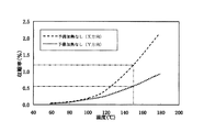
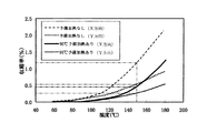
まず、本実施例における予備加熱処理を行う理由について以下にさらに詳細に説明をする。図2は、厚さ100μmのポリエチレンテレフタレート(PET)フィルムを、さまざまな加熱処理温度で1時間加熱した際の、収縮率の変動を示しているグラフである。また、図3は、樹脂基板3に予備加熱処理(例として90℃、10分間)を施したものと、予備加熱処理を施していないものを更に1時間加熱した際の、温度と収縮率の関係を示したグラフである。
First, the reason for performing the preheating process in the present embodiment will be described in more detail below. FIG. 2 is a graph showing fluctuations in shrinkage rate when a polyethylene terephthalate (PET) film having a thickness of 100 μm is heated at various heat treatment temperatures for 1 hour. Also, FIG. 3 shows the temperature and shrinkage ratio when the
樹脂基板3に使用されるフィルムは、先に示した通り2軸延伸法によって製造されており、このフィルムの延伸方向のX方向と、フィルムを固定した方向のY方向で収縮率が異なっている。そこで、このフィルムをテンションフリーな状態で加熱し、フィルムのX方向とY方向における加熱前後の長さ(それぞれをL1、L2とする)を測定した。このとき求める収縮率は、
収縮率(%)=[(L2−L1)/L1]×100
として算出している。
The film used for the
Shrinkage rate (%) = [(L2-L1) / L1] × 100
It is calculated as
この関係を示したのが図2であり、本図面に示す様に、予備加熱をしていないフィルムを加熱すると、100℃付近から収縮率は急増することが本グラフから読み取ることができる。また、光電変換素子8を構成する各層の成膜等の処理温度域(150℃以上)では、X方向の収縮率は1%以上となっているが、Y方向の収縮率は0.5%程度となっていることが判る。さらに、X方向とY方向の収縮率の差も、温度の上昇とともに増加していることが判る。
FIG. 2 shows this relationship. As shown in this drawing, it can be read from this graph that when a film that has not been preheated is heated, the shrinkage rate rapidly increases from around 100 ° C. Further, in the processing temperature range (150 ° C. or higher) such as film formation of each layer constituting the
この予備加熱をしていないフィルム、すなわち150℃での収縮率が1%を超えるフィ
ルムを樹脂基板3に使用して、光電変換装置10を製造することは、光電変換素子8のパターンを微細化して形成するときには特に好ましくない。以下にその理由を示す。
Using this unpreheated film, that is, a film having a shrinkage rate of more than 1% at 150 ° C. for the
予め予備加熱していない樹脂基板3を使用しても、実施例1で述べたように、実際に光電変換素子8を構成する各層の形成工程での処理温度以上の温度に設定して脱気処理をすれば、光電変換素子8の形成工程での加熱による樹脂基板3の収縮をある程度抑制することができるものの、図3に示すように、各層の形成工程の段階で樹脂基板3が収縮してしまうこととなる。なお、本図面に示されている予備加熱なし(X方向)、予備加熱なし(Y方向)に示されたデータは、図2に示したのと同じものである。
Even if the
この収縮は、例えば光電変換素子8を分割するとともに、分割された各光電変換素子8を直列、または並列に接続するときのパターンの微細化が進むと、この樹脂基板3の収縮は無視できない量となってしまう。
For example, the shrinkage of the
すなわち、上述した様に、光電変換素子8を微細化して分割された各光電変換素子のパターンを形成するためには、光電変換素子8間のスペースを狭小化して形成する必要があり、それとともにパターン間のズレ量のマージンも狭くしなくてはならないからである。そこで、透明電極層5、光電変換層6、裏面電極層7にパターンを形成しようとする際に、予備加熱処理をしていない150℃での収縮率が1%を超える樹脂基板3上では、パターンが所定の位置からずれてしまうという不具合が生ずることとなる。
That is, as described above, in order to form the pattern of each photoelectric conversion element divided by miniaturizing the
一方、90℃で、1時間の予備加熱処理を施した樹脂基板3は、図3に示した90℃予備加熱あり(X方向)、90℃予備加熱あり(Y方向)から、150℃でのX方向の収縮率は約0.4%であり、Y方向の収縮率は約0.3%にまで減少していることが判る。また、同一温度におけるX方向とY方向の収縮率の差も予備加熱処理をしていないものに比べて小さくなっていることが判る。光電変換素子8の形成に、このような予備加熱処理を施した樹脂基板3を使用すれば、例え、光電変換素子8に形成されるパターンを微細化したとしても、所定の位置からパターンがずれてしまう可能性を極力減少させることができる。
On the other hand, the
このように、予めテンションフリーの状態で予備加熱処理を施すことにより、光電変換素子8の形成段階での樹脂基板3の収縮を極力抑制することができる。そして、予備加熱温度が高く、加熱時間が長いほど、その効果は大きくなる。
In this way, by performing the preheating treatment in a tension-free state in advance, the shrinkage of the
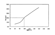
ところが、樹脂基板3を加熱するとその表面にオリゴマが析出して、樹脂基板3の平滑性が損なわれてしまう。図4は、樹脂基板3を10分間加熱した際の、加熱温度と表面粗さ(Ra)の関係を示したグラフである。
However, when the
本グラフから、温度の上昇に伴いオリゴマが大きくなることに起因して、樹脂基板3のRaは大きくなっていることが判る。また、本グラフに示すRaが20nm以上なると、後工程(支持基板1上に密着層2を介して樹脂基板3を貼り付ける工程)において、樹脂基板3と密着層2との密着力が弱くなってしまうことが出願人の実験により判明した。したがって、オリゴマの析出を抑えるためには予備加熱温度はできる限り低い方が好ましい。また、予備加熱時間が長くなると概してオリゴマの数は増加するので、予備加熱温度を低くするとともに加熱時間をできる限り短く設定して行う方がさらに好ましい。
From this graph, it can be seen that Ra of the
以上述べたように、樹脂基板3に予備加熱処理を施した際の基板の収縮率を考慮すると、温度はできるだけ高い方が望ましいが、それに反して、前述したRaを考慮すると、予備加熱温度はできるだけ低いほうが望ましい。したがって、その両方を満たす予備加熱の条件は、150℃、1時間で測定した熱収縮率が全方向で1%以下であり、かつ表面粗さ
(Ra)が20nm未満となる条件が望ましいことが判る。
As described above, considering the shrinkage rate of the substrate when the preheating treatment is performed on the
上記現象を考慮し、厚さ100μmのPETフィルムを樹脂基板3に用いた場合は、後工程を考慮して最適となる予備加熱条件を検討した結果、90℃、10分間で上記条件を満たすことが判明したので、まず、この条件下で予備加熱処理を施した樹脂基板3を用意して、実施例1に示した工程にしたがって光電変換装置10を形成した。
In consideration of the above phenomenon, when a PET film having a thickness of 100 μm is used for the
なお、90℃、10分間の予備加熱条件は、樹脂基板3の材料、厚み、樹脂基板3表面に形成される易滑性処理層、ガスバリア層の有無、後工程の処理温度などによって変わるものであり、上述した150℃、1時間で測定した熱収縮率が全方向で1%以下であり、かつ表面粗さ(Ra)が20nm未満となる予備加熱処理の条件を設定すれば良く、この条件は、上記に示した条件に拘束されるものではないことを留意されたい。
Note that the preheating conditions at 90 ° C. for 10 minutes vary depending on the material and thickness of the
まず、実施例1と同様にして、図1(a)に示す様に、支持基板1に密着層2を形成した後、図1(b)に示すように、密着層2を介して予備加熱をした樹脂基板3を、支持基板1上に貼り付ける。
First, in the same manner as in Example 1, after forming the
次に、図1(c)に示すように、密着層2と樹脂基板3との界面の脱気処理をして、密着層2と樹脂基板3を真空吸着させた後、図1(d)に示すように、光電変換素子8を形成する。樹脂基板3は、上述した最適な条件で予め予備加熱処理が施されているので、光電変換素子8のパターンずれは殆ど起こらない。
Next, as shown in FIG. 1 (c), the interface between the
最後に図1(e)に示すように、支持基板1と樹脂基板3とを分離して、目的の光電変換装置10を得ることができる。
Finally, as shown in FIG. 1 (e), the target
以上、述べたように、本実施例の製造方法は、光電変換素子8が微細パターンとする必要があるときに特に有効な方法であり、これも同様に実施例1に示した効果を得ることができるものとなる。
As described above, the manufacturing method of the present embodiment is a particularly effective method when the
1 支持基板
2 密着層
3 樹脂基板
4 空気
5 透明電極層
6 光電変換層
7 裏面電極層
8 光電変換素子
9 保護膜
10 光電変換装置
21 樹脂基板
22 剥離樹脂層
23 樹脂基板
DESCRIPTION OF
Claims (8)
硬化後に所定の軟性を持ち、かつ未硬化状態で表面を平滑とした密着層を前記支持基板に形成した後に、この密着層を完全に硬化させる工程と、
前記支持基板上に前記密着層を介して前記樹脂基板を貼り付ける工程と、
前記密着層と前記樹脂基板との界面に存在する気泡を除去するための脱気処理をして、前記密着層と前記樹脂基板とを真空吸着する工程と、
前記樹脂基板上に光電変換素子を形成する工程と、
前記支持基板と前記樹脂基板とを分離する工程と、
を含むことを特徴とする光電変換装置の製造方法。 In the method of manufacturing a photoelectric conversion device for forming a photoelectric conversion element after fixing a resin substrate on a support substrate,
A step of completely curing the adhesion layer after forming an adhesion layer having a predetermined softness after curing and having a smooth surface in an uncured state on the support substrate;
Attaching the resin substrate on the support substrate via the adhesion layer;
Deaeration treatment for removing bubbles present at the interface between the adhesion layer and the resin substrate, and vacuum adsorbing the adhesion layer and the resin substrate;
Forming a photoelectric conversion element on the resin substrate;
Separating the support substrate and the resin substrate;
A process for producing a photoelectric conversion device comprising:
The method for manufacturing a photoelectric conversion device according to claim 2, wherein the deaeration treatment is performed by heating in vacuum.
Priority Applications (1)
| Application Number | Priority Date | Filing Date | Title |
|---|---|---|---|
| JP2005037097A JP4739772B2 (en) | 2004-02-17 | 2005-02-15 | Method for manufacturing photoelectric conversion device |
Applications Claiming Priority (5)
| Application Number | Priority Date | Filing Date | Title |
|---|---|---|---|
| JP2004039136 | 2004-02-17 | ||
| JP2004039136 | 2004-02-17 | ||
| JP2004066487 | 2004-03-10 | ||
| JP2004066487 | 2004-03-10 | ||
| JP2005037097A JP4739772B2 (en) | 2004-02-17 | 2005-02-15 | Method for manufacturing photoelectric conversion device |
Publications (2)
| Publication Number | Publication Date |
|---|---|
| JP2005294807A true JP2005294807A (en) | 2005-10-20 |
| JP4739772B2 JP4739772B2 (en) | 2011-08-03 |
Family
ID=35327344
Family Applications (1)
| Application Number | Title | Priority Date | Filing Date |
|---|---|---|---|
| JP2005037097A Expired - Lifetime JP4739772B2 (en) | 2004-02-17 | 2005-02-15 | Method for manufacturing photoelectric conversion device |
Country Status (1)
| Country | Link |
|---|---|
| JP (1) | JP4739772B2 (en) |
Cited By (4)
| Publication number | Priority date | Publication date | Assignee | Title |
|---|---|---|---|---|
| WO2010001927A1 (en) * | 2008-07-02 | 2010-01-07 | シャープ株式会社 | Solar battery module and method for manufacturing the same |
| JP2011258996A (en) * | 2011-09-29 | 2011-12-22 | Sharp Corp | Solar cell module and its manufacturing method |
| JP2013030779A (en) * | 2006-06-05 | 2013-02-07 | Dow Corning Corp | Solar cell including silicone resin layer |
| KR101298313B1 (en) * | 2006-08-14 | 2013-08-20 | 엘지디스플레이 주식회사 | Fabricating method of flexible Display |
Citations (6)
| Publication number | Priority date | Publication date | Assignee | Title |
|---|---|---|---|---|
| JPH01105581A (en) * | 1987-10-19 | 1989-04-24 | Sanyo Electric Co Ltd | Manufacture of photovoltaic device |
| JPH04296061A (en) * | 1991-03-25 | 1992-10-20 | Sanyo Electric Co Ltd | Manufacture of photovoltaic device |
| JPH05102500A (en) * | 1991-10-07 | 1993-04-23 | Sanyo Electric Co Ltd | Manufacture of photoelectromotive device |
| JP2975766B2 (en) * | 1992-05-13 | 1999-11-10 | 三洋電機株式会社 | Method for manufacturing flexible thin film solar cell |
| JP2003504877A (en) * | 1999-07-13 | 2003-02-04 | アイトゲネーシシエ テクニシエ ホッホシューレ (エーテーハー) | Flexible thin-film solar cells |
| JP2005129713A (en) * | 2003-10-23 | 2005-05-19 | Sharp Corp | Thin film solar cell and manufacturing method thereof |
-
2005
- 2005-02-15 JP JP2005037097A patent/JP4739772B2/en not_active Expired - Lifetime
Patent Citations (7)
| Publication number | Priority date | Publication date | Assignee | Title |
|---|---|---|---|---|
| JPH01105581A (en) * | 1987-10-19 | 1989-04-24 | Sanyo Electric Co Ltd | Manufacture of photovoltaic device |
| JP2680582B2 (en) * | 1987-10-19 | 1997-11-19 | 三洋電機株式会社 | Method for manufacturing photovoltaic device |
| JPH04296061A (en) * | 1991-03-25 | 1992-10-20 | Sanyo Electric Co Ltd | Manufacture of photovoltaic device |
| JPH05102500A (en) * | 1991-10-07 | 1993-04-23 | Sanyo Electric Co Ltd | Manufacture of photoelectromotive device |
| JP2975766B2 (en) * | 1992-05-13 | 1999-11-10 | 三洋電機株式会社 | Method for manufacturing flexible thin film solar cell |
| JP2003504877A (en) * | 1999-07-13 | 2003-02-04 | アイトゲネーシシエ テクニシエ ホッホシューレ (エーテーハー) | Flexible thin-film solar cells |
| JP2005129713A (en) * | 2003-10-23 | 2005-05-19 | Sharp Corp | Thin film solar cell and manufacturing method thereof |
Cited By (6)
| Publication number | Priority date | Publication date | Assignee | Title |
|---|---|---|---|---|
| JP2013030779A (en) * | 2006-06-05 | 2013-02-07 | Dow Corning Corp | Solar cell including silicone resin layer |
| KR101298313B1 (en) * | 2006-08-14 | 2013-08-20 | 엘지디스플레이 주식회사 | Fabricating method of flexible Display |
| WO2010001927A1 (en) * | 2008-07-02 | 2010-01-07 | シャープ株式会社 | Solar battery module and method for manufacturing the same |
| JP2010016074A (en) * | 2008-07-02 | 2010-01-21 | Sharp Corp | Solar cell module, and its manufacturing method |
| US8993875B2 (en) | 2008-07-02 | 2015-03-31 | Sharp Kabushiki Kaisha | Solar battery module and method for manufacturing the same |
| JP2011258996A (en) * | 2011-09-29 | 2011-12-22 | Sharp Corp | Solar cell module and its manufacturing method |
Also Published As
| Publication number | Publication date |
|---|---|
| JP4739772B2 (en) | 2011-08-03 |
Similar Documents
| Publication | Publication Date | Title |
|---|---|---|
| JP5200538B2 (en) | Thin glass laminate and method for manufacturing display device using thin glass laminate | |
| TWI377646B (en) | Substrate structures applied in flexible electrical devices and fabrication method thereof | |
| TWI310207B (en) | Thin film device supply body, method of fabricating thin film device, method of transfer, method of fabricating semiconductor device, and electronic equipment | |
| CN1444436A (en) | Printed circuit board and making method thereof | |
| JP2006041135A (en) | Electronic device and manufacturing method thereof | |
| CN1444270A (en) | COF flexible printed circuit board and method for manufacturing the same | |
| JP2017535824A (en) | Array substrate and manufacturing method thereof, flexible display panel and display device | |
| JP2016521247A (en) | Glass structure and method of manufacturing and processing glass structure | |
| JP4739772B2 (en) | Method for manufacturing photoelectric conversion device | |
| CN110098225B (en) | Flexible display panel and preparation method thereof | |
| CN104736340A (en) | Glass laminate and manufacturing method therefor, and support base with silicone resin layer | |
| CN1233521C (en) | Method for producing metal laminated products | |
| US20090050352A1 (en) | Substrate structures for flexible electronic devices and fabrication methods thereof | |
| KR102185633B1 (en) | Flexible substrate, manufacturing method thereof, and flexible electronic device including the same | |
| CN1713979A (en) | Method for producing heat-resistant flexible laminate | |
| JP2005300930A (en) | Method for manufacturing optical and electrical consolidated substrate | |
| JP7349302B2 (en) | Method for manufacturing fluorine-containing core base material and method for manufacturing substrate for flexible printed wiring board | |
| JP2017193730A (en) | Copper foil with carrier comprising sputtering-type inorganic composite film and method for producing the same | |
| JP2005011877A (en) | Circuit pattern forming method | |
| CN112526660B (en) | Method for manufacturing nano-grating on curved surface, optical device and electronic equipment | |
| JP5760818B2 (en) | Manufacturing method of laminate | |
| TWI491324B (en) | Flexible substrate, display apparatus using the same and manufacturing method thereof | |
| JP4041356B2 (en) | Transfer sheet manufacturing method, wiring board and manufacturing method thereof | |
| JP4496719B2 (en) | Circuit pattern transfer mold and manufacturing method thereof | |
| JPH0694203B2 (en) | Method for manufacturing silicone rubber structure |
Legal Events
| Date | Code | Title | Description |
|---|---|---|---|
| A621 | Written request for application examination |
Free format text: JAPANESE INTERMEDIATE CODE: A621 Effective date: 20071204 |
|
| RD03 | Notification of appointment of power of attorney |
Free format text: JAPANESE INTERMEDIATE CODE: A7423 Effective date: 20071204 |
|
| A977 | Report on retrieval |
Free format text: JAPANESE INTERMEDIATE CODE: A971007 Effective date: 20100323 |
|
| TRDD | Decision of grant or rejection written | ||
| A01 | Written decision to grant a patent or to grant a registration (utility model) |
Free format text: JAPANESE INTERMEDIATE CODE: A01 Effective date: 20110419 |
|
| A01 | Written decision to grant a patent or to grant a registration (utility model) |
Free format text: JAPANESE INTERMEDIATE CODE: A01 |
|
| A61 | First payment of annual fees (during grant procedure) |
Free format text: JAPANESE INTERMEDIATE CODE: A61 Effective date: 20110428 |
|
| R150 | Certificate of patent or registration of utility model |
Ref document number: 4739772 Country of ref document: JP Free format text: JAPANESE INTERMEDIATE CODE: R150 Free format text: JAPANESE INTERMEDIATE CODE: R150 |
|
| FPAY | Renewal fee payment (event date is renewal date of database) |
Free format text: PAYMENT UNTIL: 20140513 Year of fee payment: 3 |
|
| S533 | Written request for registration of change of name |
Free format text: JAPANESE INTERMEDIATE CODE: R313533 |
|
| R350 | Written notification of registration of transfer |
Free format text: JAPANESE INTERMEDIATE CODE: R350 |
|
| R250 | Receipt of annual fees |
Free format text: JAPANESE INTERMEDIATE CODE: R250 |
|
| R250 | Receipt of annual fees |
Free format text: JAPANESE INTERMEDIATE CODE: R250 |
|
| R250 | Receipt of annual fees |
Free format text: JAPANESE INTERMEDIATE CODE: R250 |
|
| R250 | Receipt of annual fees |
Free format text: JAPANESE INTERMEDIATE CODE: R250 |
|
| EXPY | Cancellation because of completion of term |