JP2005294742A - Performance information measuring method of exposing device and performance information measuring apparatus, and exposing method - Google Patents
Performance information measuring method of exposing device and performance information measuring apparatus, and exposing method Download PDFInfo
- Publication number
- JP2005294742A JP2005294742A JP2004111177A JP2004111177A JP2005294742A JP 2005294742 A JP2005294742 A JP 2005294742A JP 2004111177 A JP2004111177 A JP 2004111177A JP 2004111177 A JP2004111177 A JP 2004111177A JP 2005294742 A JP2005294742 A JP 2005294742A
- Authority
- JP
- Japan
- Prior art keywords
- information
- optical system
- projection optical
- wafer
- exposure apparatus
- Prior art date
- Legal status (The legal status is an assumption and is not a legal conclusion. Google has not performed a legal analysis and makes no representation as to the accuracy of the status listed.)
- Pending
Links
Images
Classifications
-
- G—PHYSICS
- G03—PHOTOGRAPHY; CINEMATOGRAPHY; ANALOGOUS TECHNIQUES USING WAVES OTHER THAN OPTICAL WAVES; ELECTROGRAPHY; HOLOGRAPHY
- G03F—PHOTOMECHANICAL PRODUCTION OF TEXTURED OR PATTERNED SURFACES, e.g. FOR PRINTING, FOR PROCESSING OF SEMICONDUCTOR DEVICES; MATERIALS THEREFOR; ORIGINALS THEREFOR; APPARATUS SPECIALLY ADAPTED THEREFOR
- G03F7/00—Photomechanical, e.g. photolithographic, production of textured or patterned surfaces, e.g. printing surfaces; Materials therefor, e.g. comprising photoresists; Apparatus specially adapted therefor
- G03F7/70—Microphotolithographic exposure; Apparatus therefor
- G03F7/70483—Information management; Active and passive control; Testing; Wafer monitoring, e.g. pattern monitoring
- G03F7/70605—Workpiece metrology
- G03F7/70616—Monitoring the printed patterns
- G03F7/70641—Focus
Landscapes
- Physics & Mathematics (AREA)
- General Physics & Mathematics (AREA)
- Length Measuring Devices By Optical Means (AREA)
- Exposure And Positioning Against Photoresist Photosensitive Materials (AREA)
- Exposure Of Semiconductors, Excluding Electron Or Ion Beam Exposure (AREA)
Abstract
Description
本発明は、露光装置の性能情報計測方法及び性能情報計測装置、並びに露光方法に係り、更に詳しくは、半導体素子(集積回路)や液晶表示素子などを製造するリソグラフィ工程で使用される露光装置の性能を評価するための情報を計測する性能情報計測方法及び性能情報計測装置、並びに前記性能情報計測方法によって性能を評価するための情報が計測された露光装置を用いて露光を行う露光方法に関する。 The present invention relates to a performance information measuring method, a performance information measuring device, and an exposure method for an exposure apparatus, and more particularly, to an exposure apparatus used in a lithography process for manufacturing a semiconductor element (integrated circuit), a liquid crystal display element, and the like. The present invention relates to a performance information measuring method and a performance information measuring apparatus for measuring information for evaluating performance, and an exposure method for performing exposure using an exposure apparatus in which information for evaluating performance is measured by the performance information measuring method.
従来より、半導体素子又は液晶表示素子等を製造するためのフォトリソグラフィ工程では、マスク又はレチクル(以下、「レチクル」と総称する)のパターンを、投影光学系を介して表面にレジスト等の感光剤が塗布されたウエハ又はガラスプレート等の基板(以下、適宜「ウエハ」ともいう)上に転写する投影露光装置、例えばステップ・アンド・リピート方式の縮小投影露光装置(いわゆるステッパ)や、ステップ・アンド・スキャン方式の走査型投影露光装置(いわゆるスキャニング・ステッパ)等が用いられている。 Conventionally, in a photolithography process for manufacturing a semiconductor element, a liquid crystal display element, or the like, a mask or a reticle (hereinafter, collectively referred to as “reticle”) pattern is exposed to a photosensitive agent such as a resist on the surface via a projection optical system. A projection exposure apparatus that transfers onto a substrate such as a wafer or glass plate (hereinafter also referred to as “wafer” as appropriate), such as a step-and-repeat reduction projection exposure apparatus (so-called stepper), A scanning type scanning exposure apparatus (so-called scanning stepper) or the like is used.
ところで、半導体素子(集積回路)等は年々高集積化しており、これに伴い投影露光装置には、一層の性能の向上が要求されるようになってきた。例えば、投影露光装置の解像力を向上させ、より微細なパターンを精度良く転写するためには、投影光学系の光学性能を向上させることが必要である。このため、投影光学系の光学特性(結像特性を含む)を正確に計測し、評価することが重要となっている。さらに、走査型投影露光装置では、レチクルとウエハとを同期移動させながらパターンを投影光学系を介してウエハ上に転写しているため、ウエハの移動面の傾斜及びうねりが解像力に大きく影響する。 By the way, semiconductor elements (integrated circuits) and the like have been highly integrated year by year, and accordingly, further improvement in performance has been required for projection exposure apparatuses. For example, in order to improve the resolution of the projection exposure apparatus and transfer a finer pattern with high accuracy, it is necessary to improve the optical performance of the projection optical system. For this reason, it is important to accurately measure and evaluate the optical characteristics (including imaging characteristics) of the projection optical system. Further, in the scanning projection exposure apparatus, the pattern and the wafer are transferred onto the wafer via the projection optical system while the reticle and the wafer are moved synchronously. Therefore, the inclination and waviness of the moving surface of the wafer greatly affect the resolving power.
投影光学系の光学特性、例えば像面湾曲は、投影光学系の視野内の複数の計測点における最適なウエハの光軸方向位置(以下、適宜「最良フォーカス位置」と呼ぶ)に基づいて最小自乗法等の統計処理により求められる。従って、像面湾曲を求めるには、投影光学系の視野内の各計測点における最良フォーカス位置を精度良く計測する必要がある。 The optical characteristics of the projection optical system, for example, the curvature of field, are minimized based on the optimal position in the optical axis direction of the wafer (hereinafter referred to as “best focus position” as appropriate) at a plurality of measurement points in the field of view of the projection optical system. It is obtained by statistical processing such as multiplication. Therefore, in order to obtain the curvature of field, it is necessary to accurately measure the best focus position at each measurement point in the field of view of the projection optical system.
従来の投影露光装置における最良フォーカス位置を計測する方法としては、例えば、所定のテスト用のパターンを投影光学系の光軸方向に関する複数の位置でテスト用ウエハに転写し、そのテスト用ウエハを現像して得られるレジスト像(転写されたパターンの像)の形成状態を計測し、その形成状態と投影光学系の光軸方向に関するウエハの位置(以下、適宜「フォーカス位置」ともいう)との相関関係に基づいて最良フォーカス位置を判断する方法、例えばレジスト像のパターン線幅を上記の形成状態として計測する、いわゆるCD(線幅)−フォーカス法などが知られている。 As a method for measuring the best focus position in a conventional projection exposure apparatus, for example, a predetermined test pattern is transferred to a test wafer at a plurality of positions in the optical axis direction of the projection optical system, and the test wafer is developed. The formation state of the resist image (transferred pattern image) obtained in this way is measured, and the correlation between the formation state and the wafer position in the optical axis direction of the projection optical system (hereinafter also referred to as “focus position” as appropriate) A method for determining the best focus position based on the relationship, for example, a so-called CD (line width) -focus method for measuring the pattern line width of the resist image as the above-described formation state is known.
しかしながら、最良フォーカス位置の計測に用いられるテスト用ウエハは、必ずしもその表面が平坦ではないため、計測される最良フォーカス位置にウエハの表面形状に起因する誤差が含まれるおそれがあった。 However, since the surface of the test wafer used for measuring the best focus position is not necessarily flat, there is a possibility that an error due to the surface shape of the wafer is included in the measured best focus position.
そこで、投影露光装置に設けられているオートフォーカス装置等を用いて、ウエハの表面形状を計測し、その計測結果に基づいて最良フォーカス位置を補正する方法、あるいは計測点の数を多くするとともに計測点間の間隔を小さくして各計測点における最良フォーカス位置を計測し、統計処理によってウエハの表面形状の影響を小さくする方法などが用いられていた。さらに、特別に研磨してウエハ表面の平坦度を高めた、いわゆる超平坦度ウエハ(スーパーフラットウエハ)等を用いて最良フォーカス位置を計測することも行なわれていた。 Therefore, a method of measuring the surface shape of the wafer using an autofocus device provided in the projection exposure apparatus and correcting the best focus position based on the measurement result, or increasing the number of measurement points and measuring. A method of measuring the best focus position at each measurement point by reducing the interval between the points and reducing the influence of the surface shape of the wafer by statistical processing has been used. Further, the best focus position has been measured using a so-called super flat wafer (super flat wafer) or the like that is specially polished to increase the flatness of the wafer surface.
しかしながら、半導体素子等が高集積化するにつれて、上述したオートフォーカス装置等を用いる方法では、必要とされる計測精度を満足することが困難となり、補正を行なっても誤差が残留(残存)する可能性が生じてきた。 However, as semiconductor elements and the like become highly integrated, it is difficult to satisfy the required measurement accuracy with the above-described method using the autofocus device, and errors may remain (remain) even after correction. Sex has arisen.
また、上述した計測点の数を多くする方法では、計測に要する時間が大きく増加し、スループットを低下させるという不都合があった。 In addition, the above-described method for increasing the number of measurement points has a disadvantage in that the time required for measurement is greatly increased and throughput is lowered.
さらに、上述した超平坦度ウエハ等を用いる方法では、コストが高くなるとともに、ウエハホルダ表面あるいはウエハ裏面のゴミ等に起因してウエハ表面の平坦度が低下し、計測結果に誤差が含まれるおそれがあった。 Furthermore, in the method using the above-described ultra-flatness wafer or the like, the cost becomes high, and the flatness of the wafer surface is lowered due to dust on the wafer holder surface or the wafer back surface, and there is a possibility that the measurement result includes an error. there were.
また、将来的に、半導体素子はさらに高集積化し、これに伴い、露光装置に要求される転写精度はますます厳しくなることは確実である。そこで、将来の露光装置に許容されるトータルオーバーレイ誤差を考慮すれば、上記計測結果に含まれる誤差に起因する転写誤差も無視できなくなってきている。 Further, in the future, semiconductor devices will be further highly integrated, and as a result, it is certain that the transfer accuracy required for the exposure apparatus will become increasingly severe. In view of the total overlay error allowed in the future exposure apparatus, the transfer error due to the error included in the measurement result cannot be ignored.
本発明は、かかる事情の下になされたものであり、その第1の目的は、スループットを低下させることなく、低コストで精度良く露光装置の性能を評価するための情報を計測することができる露光装置の性能情報計測方法及び性能情報計測装置を提供することにある。 The present invention has been made under such circumstances, and a first object thereof is to measure information for accurately evaluating the performance of an exposure apparatus at a low cost without reducing the throughput. An object of the present invention is to provide a performance information measuring method and a performance information measuring apparatus for an exposure apparatus.
また、本発明の第2の目的は、高精度な露光を実現できる露光方法を提供することにある。 A second object of the present invention is to provide an exposure method capable of realizing highly accurate exposure.
請求項1に記載の発明は、第1面上のパターンを投影光学系(PL)を介して第2面上に転写する露光装置の性能を評価するための情報を計測する露光装置の性能情報計測方法であって、複数の計測用パターン(PUi,j)が形成されたマスク(RT)を前記第1面上に配置し、前記投影光学系の前記第2面側に配置された表面に感光層を有する物体(WT)の位置を前記投影光学系の光軸方向に変化させ、その光軸方向の位置毎に、前記投影光学系を介して前記計測用パターンの像を前記物体上の第1の領域内の複数の部分領域にそれぞれ形成する第1工程と;前記物体の位置を前記投影光学系の光軸方向に変化させ、その光軸方向の位置毎に、前記投影光学系を介して前記計測用パターンの像を前記物体上の第2の領域内の複数の部分領域にそれぞれ形成する第2工程と;前記第1工程で形成された前記計測用パターンの像の形成状態に関する情報に基づいて前記投影光学系の第1のフォーカス情報を求める第3工程と;前記第2工程で形成された前記計測用パターンの像の形成状態に関する情報に基づいて前記投影光学系の第2のフォーカス情報を求める第4工程と;前記第1のフォーカス情報と前記第2のフォーカス情報とに基づいて、前記物体の表面形状情報を求める第5工程と;を含む露光装置の性能情報計測方法である。 According to the first aspect of the present invention, the performance information of the exposure apparatus that measures information for evaluating the performance of the exposure apparatus that transfers the pattern on the first surface onto the second surface via the projection optical system (PL). In the measurement method, a mask (R T ) on which a plurality of measurement patterns (PU i, j ) are formed is disposed on the first surface, and is disposed on the second surface side of the projection optical system. The position of an object (W T ) having a photosensitive layer on the surface is changed in the optical axis direction of the projection optical system, and the image of the measurement pattern is transferred via the projection optical system for each position in the optical axis direction. A first step of forming each of a plurality of partial regions in a first region on the object; changing the position of the object in the optical axis direction of the projection optical system, and performing the projection for each position in the optical axis direction A plurality of partial areas in the second area on the object are obtained by imaging the measurement pattern image via an optical system. A second step of forming each of the projection optical system, a third step of obtaining first focus information of the projection optical system based on information relating to an image formation state of the measurement pattern formed in the first step; A fourth step of obtaining second focus information of the projection optical system based on information relating to a formation state of the image of the measurement pattern formed in two steps; the first focus information and the second focus information; And a fifth step of obtaining surface shape information of the object on the basis of
本明細書において、フォーカス情報とは、最良フォーカス位置に限らず、物体の表面形状を求める基となるフォーカス情報の全てを含む。 In this specification, the focus information is not limited to the best focus position, but includes all focus information that is a basis for obtaining the surface shape of the object.
これによれば、投影光学系の光軸方向に関する物体の位置毎に、投影光学系を介して計測用パターンの像を物体上の第1の領域内の複数の部分領域にそれぞれ形成し(第1工程)、次に、投影光学系の光軸方向に関する物体の位置毎に、投影光学系を介して計測用パターンの像を物体上の第2の領域内の複数の部分領域にそれぞれ形成する(第2工程)。この結果、第1の領域内及び第2の領域内の各部分領域には、転写時の光軸方向に関する物体の位置が異なる計測用パターンの像が形成される。 According to this, for each position of the object in the optical axis direction of the projection optical system, an image of the measurement pattern is formed in each of a plurality of partial areas in the first area on the object via the projection optical system (first Step 1) Next, for each position of the object in the optical axis direction of the projection optical system, an image of the measurement pattern is formed in each of a plurality of partial areas in the second area on the object via the projection optical system. (Second step). As a result, images of measurement patterns having different object positions in the optical axis direction during transfer are formed in the partial areas in the first area and the second area.
さらに、第1工程で形成された計測用パターンの像の形成状態に関する情報に基づいて投影光学系の第1のフォーカス情報を求め(第3工程)、第2工程で形成された計測用パターンの像の形成状態に関する情報に基づいて投影光学系の第2のフォーカス情報を求める(第4工程)。この結果、同一の計測用パターンに由来する2つのフォーカス情報が得られる。 Further, the first focus information of the projection optical system is obtained based on the information regarding the image formation state of the measurement pattern formed in the first step (third step), and the measurement pattern formed in the second step is obtained. Second focus information of the projection optical system is obtained based on information relating to the image formation state (fourth step). As a result, two pieces of focus information derived from the same measurement pattern are obtained.
そして、第1のフォーカス情報と第2のフォーカス情報とに基づいて、物体の表面形状情報を求める(第5工程)。例えば、同一の計測用パターンに由来する第1のフォーカス情報と第2のフォーカス情報との差から、投影光学系の光軸方向に関する第1の領域と第2の領域との位置の差、すなわち、物体表面の平坦度を求めることができる。さらに、露光装置の性能を評価するための情報の計測結果が物体の表面形状に依存する成分を含む場合には、ここで求められた物体の表面形状情報に基づいて物体の表面形状に依存する成分を補正することにより露光装置の性能に関する情報のみを抽出することができる。すなわち、高価な超平坦度ウエハ等を必要とせずに、しかも従来と同等の計測点数であっても、従来に比べて精度良く露光装置の性能を評価するための情報を計測することができる。 Then, surface shape information of the object is obtained based on the first focus information and the second focus information (fifth step). For example, from the difference between the first focus information and the second focus information derived from the same measurement pattern, the difference in position between the first region and the second region in the optical axis direction of the projection optical system, that is, The flatness of the object surface can be obtained. Furthermore, when the measurement result of the information for evaluating the performance of the exposure apparatus includes a component that depends on the surface shape of the object, it depends on the surface shape of the object based on the surface shape information of the object obtained here. By correcting the components, only information relating to the performance of the exposure apparatus can be extracted. That is, it is possible to measure information for evaluating the performance of the exposure apparatus with higher accuracy than in the past without requiring an expensive ultra-flatness wafer or the like and with the same number of measurement points as in the past.
従って、請求項1に記載の発明によれば、スループットを低下させることなく、低コストで精度良く露光装置の性能を評価するための情報を計測することが可能となる。 Therefore, according to the first aspect of the present invention, it is possible to measure information for accurately evaluating the performance of the exposure apparatus at a low cost without reducing the throughput.
この場合において、請求項2に記載の露光装置の性能情報計測方法の如く、前記第1のフォーカス情報と前記第2のフォーカス情報と前記表面形状情報とに基づいて、前記露光装置の性能を評価するための情報を求める第6工程を更に含むこととすることができる。
In this case, the performance of the exposure apparatus is evaluated based on the first focus information, the second focus information, and the surface shape information, as in the exposure apparatus performance information measuring method according to
この場合において、請求項3に記載の露光装置の性能情報計測方法の如く、前記第1工程に先だって、前記投影光学系を調整する第7工程を更に含み、前記第1工程及び第2工程では、前記マスクと前記物体とを同期移動させつつ前記計測用パターンの像を前記物体上に形成することとすることができる。
In this case, as in the method for measuring performance information of an exposure apparatus according to
この場合において、前記露光装置の性能を評価するための情報としては、種々のものが考えられるが、請求項4に記載の露光装置の性能情報計測方法の如く、前記露光装置の性能を評価するための情報は、前記投影光学系の光学特性に関する情報を含むこととしても良い。
In this case, various kinds of information for evaluating the performance of the exposure apparatus can be considered. As in the exposure apparatus performance information measuring method according to
この場合において、請求項5に記載の露光装置の性能情報計測方法の如く、前記第1工程に先だって、前記投影光学系の光学特性に関する情報に基づいて、前記投影光学系を調整する工程を更に含むこととすることができる。
In this case, the step of adjusting the projection optical system based on the information on the optical characteristics of the projection optical system prior to the first step, as in the performance information measuring method of the exposure apparatus according to
上記請求項2〜5に記載の各露光装置の性能情報計測方法において、前記露光装置の性能を評価するための情報としては、種々のものが考えられるが、請求項6に記載の露光装置の性能情報計測方法の如く、前記露光装置の性能を評価するための情報は、前記物体の走査特性に関する情報を含むこととすることができる。
In the performance information measuring method for each exposure apparatus according to any one of
本明細書において、物体の走査特性に関する情報とは、走査露光時における物体の移動面の傾斜やうねり等の情報を含む。 In this specification, the information relating to the scanning characteristics of the object includes information such as the inclination and waviness of the moving surface of the object during scanning exposure.
上記請求項1〜6に記載の各露光装置の性能情報計測方法において、請求項7に記載の露光装置の性能情報計測方法の如く、前記第1工程及び第2工程では、前記物体の前記投影光学系の光軸方向の位置変化は、前記物体を傾斜させることなく行なうこととすることができる。
7. The performance information measuring method of each exposure apparatus according to
上記請求項1〜7に記載の各露光装置の性能情報計測方法において、請求項8に記載の露光装置の性能情報計測方法の如く、前記物体の表面形状情報は、前記第1のフォーカス情報と第2のフォーカス情報との差に基づいて算出されることとしても良い。
The performance information measurement method for each exposure apparatus according to any one of
上記請求項1〜8に記載の各露光装置の性能情報計測方法において、請求項9に記載の露光装置の性能情報計測方法の如く、前記計測用パターンは、特定の方向に等間隔で配置されていることとすることができる。
9. The performance information measuring method of each exposure apparatus according to
この場合において、請求項10に記載の露光装置の性能情報計測方法の如く、前記特定の方向に関する前記計測用パターン間の距離をLとし、前記投影光学系の投影倍率をMとすると、前記第1の領域と第2の領域との前記特定の方向に関する距離はL×Mであることとしても良い。
In this case, when the distance between the measurement patterns in the specific direction is L and the projection magnification of the projection optical system is M, as in the performance information measurement method for an exposure apparatus according to
上記請求項1〜10に記載の各露光装置の性能情報計測方法において、前記計測用パターンとしては、種々のパターンが考えられるが、請求項11に記載の露光装置の性能情報計測方法の如く、前記計測用パターンは、ラインアンドスペースパターンを含むこととすることができる。
In the performance information measuring method for each exposure apparatus according to any one of
上記請求項1〜11に記載の各露光装置の性能情報計測方法において、前記計測用パターンの像の形成状態に関する情報としては、種々の情報が考えられるが、請求項12に記載の露光装置の性能情報計測方法の如く、前記計測用パターンの像の形成状態に関する情報は、前記計測用パターンの像の線幅情報を含むこととすることができる。
In the performance information measuring method for each exposure apparatus according to any one of
請求項13に記載の発明は、マスク(R)のパターンを投影光学系(PL)を介して基板ステージ(20)に保持された基板(W)上に転写する露光装置(100)の性能を評価するための情報を計測する性能情報計測装置であって、前記基板ステージの位置を前記投影光学系の光軸方向に変化させ、その光軸方向の位置毎に、前記投影光学系を介して計測用パターン(PUi,j)の像を前記基板ステージに保持された表面に感光層を有する物体(WT)上の第1の領域内の複数の部分領域にそれぞれ形成する第1の像形成装置と;前記基板ステージの位置を前記投影光学系の光軸方向に変化させ、その光軸方向の位置毎に、前記投影光学系を介して前記計測用パターンの像を前記物体上の第2の領域内の複数の部分領域にそれぞれ形成する第2の像形成装置と;前記第1の像形成装置にて形成された前記計測用パターンの像の形成状態に基づいて前記投影光学系の第1のフォーカス情報を求める第1のフォーカス情報取得装置と;前記第2の像形成装置にて形成された前記計測用パターンの像の形成状態に基づいて前記投影光学系の第2のフォーカス情報を求める第2のフォーカス情報取得装置と;前記第1のフォーカス情報と前記第2のフォーカス情報とに基づいて、前記物体の表面形状情報を求める形状情報取得装置と;前記第1のフォーカス情報と前記第2のフォーカス情報と前記表面形状情報とに基づいて、前記露光装置の性能を評価するための情報を算出する算出装置と;を含む性能情報計測装置である。
The invention according to
これによれば、第1の像形成装置及び第2の像形成装置では、基板ステージの位置を投影光学系の光軸方向に変化させ、その光軸方向の位置毎に、投影光学系を介して計測用パターンの像を物体上の第1の領域内及び第2の領域内の複数の部分領域にそれぞれ形成する。その結果、第1の領域と第2の領域に同一の計測用パターンに由来する転写像がそれぞれ形成される。 According to this, in the first image forming apparatus and the second image forming apparatus, the position of the substrate stage is changed in the optical axis direction of the projection optical system, and each position in the optical axis direction is passed through the projection optical system. Thus, images of the measurement pattern are formed in a plurality of partial areas in the first area and the second area on the object, respectively. As a result, transfer images derived from the same measurement pattern are formed in the first region and the second region, respectively.
また、第1のフォーカス情報取得装置では、第1の像形成装置にて形成された計測用パターンの像の形成状態に基づいて投影光学系の第1のフォーカス情報を求め、第2のフォーカス情報取得装置では、第2の像形成装置にて形成された計測用パターンの像の形成状態に基づいて投影光学系の第2のフォーカス情報を求める。その結果、物体上の異なる領域で同一の計測用パターンに由来するフォーカス情報が得られる。 Further, the first focus information acquisition device obtains first focus information of the projection optical system based on the formation state of the image of the measurement pattern formed by the first image forming device, and the second focus information. The acquisition device obtains second focus information of the projection optical system based on the formation state of the measurement pattern image formed by the second image forming device. As a result, focus information derived from the same measurement pattern is obtained in different regions on the object.
そして、形状情報取得装置では、第1のフォーカス情報と第2のフォーカス情報とに基づいて物体の表面形状情報を求める。例えば、同一の計測用パターンに由来する第1のフォーカス情報と第2のフォーカス情報との差から、投影光学系の光軸方向に関する第1の領域と第2の領域との位置の差、すなわち、物体表面の平坦度を求めることができる。 Then, the shape information acquisition device obtains the surface shape information of the object based on the first focus information and the second focus information. For example, from the difference between the first focus information and the second focus information derived from the same measurement pattern, the difference in position between the first region and the second region in the optical axis direction of the projection optical system, that is, The flatness of the object surface can be obtained.
さらに、算出装置では、第1のフォーカス情報と第2のフォーカス情報と表面形状情報とに基づいて露光装置の性能を評価するための情報を算出する。その結果、物体の表面形状に依存する成分が補正された露光装置の性能を評価するための情報が得られる。すなわち、高価な超平坦度ウエハ等を必要とせずに、しかも従来と同等の計測点数であっても、従来に比べて精度良く露光装置の性能を評価するための情報を計測することができる。 Further, the calculation apparatus calculates information for evaluating the performance of the exposure apparatus based on the first focus information, the second focus information, and the surface shape information. As a result, information for evaluating the performance of the exposure apparatus in which the component depending on the surface shape of the object is corrected can be obtained. That is, it is possible to measure information for evaluating the performance of the exposure apparatus with higher accuracy than in the past without requiring an expensive ultra-flatness wafer or the like and with the same number of measurement points as in the past.
従って、請求項13に記載の性能情報計測装置によれば、スループットを低下させることなく、低コストで精度良く露光装置の性能を評価するための情報を計測することが可能となる。 Therefore, according to the performance information measuring apparatus of the thirteenth aspect, it is possible to measure information for accurately evaluating the performance of the exposure apparatus at a low cost without reducing the throughput.
請求項14に記載の露光方法は、露光用のエネルギビームをマスク(R)に照射し、前記マスクに形成されたパターンを投影光学系(PL)を介して基板(W)上に転写する露光方法であって、請求項4に記載の露光装置の性能情報計測方法によって計測された前記投影光学系の光学特性に関する情報を考慮して前記投影光学系を調整する工程と;前記調整された投影光学系を介して前記マスクに形成されたパターンを前記基板に転写する工程と;を含む露光方法である。
The exposure method according to claim 14, wherein the mask (R) is irradiated with an energy beam for exposure, and the pattern formed on the mask is transferred onto the substrate (W) via the projection optical system (PL). A method for adjusting the projection optical system in consideration of information on optical characteristics of the projection optical system measured by the method for measuring performance information of an exposure apparatus according to
これによれば、請求項4に記載の露光装置の性能情報計測方法によって計測された投影光学系の光学特性に関する情報を考慮して最適な転写が行えるように投影光学系が調整され、その調整された投影光学系を介してマスクに形成されたパターンを基板上に転写するので、微細パターンを基板上に高精度に転写することができる。
According to this, the projection optical system is adjusted so that optimum transfer can be performed in consideration of the information on the optical characteristics of the projection optical system measured by the performance information measuring method of the exposure apparatus according to
請求項15に記載の露光方法は、マスク(R)と基板(W)とを同期移動して、前記マスクのパターンを投影光学系(PL)を介して基板上に転写する露光方法であって、請求項6に記載の露光装置の性能情報計測方法によって前記基板の走査特性に関する情報を計測する工程と;前記マスクと前記基板とを同期移動するとともに、該同期移動中に前記走査特性に関する情報の計測結果を考慮して前記基板の位置を制御しつつ、前記マスクのパターンを前記投影光学系を介して前記基板上に転写する工程と;を含む露光方法である。
The exposure method according to
これによれば、請求項6に記載の露光装置の性能情報計測方法によって基板の走査特性に関する情報が計測され、該計測結果を考慮してマスクと基板とを同期制御しつつ、マスクのパターンが投影光学系を介して基板上に転写される。このため、微細パターンを基板上に高精度に転写することができる。
According to this, information on the scanning characteristics of the substrate is measured by the performance information measuring method of the exposure apparatus according to
以下、本発明の一実施形態を図1〜図13に基づいて説明する。 Hereinafter, an embodiment of the present invention will be described with reference to FIGS.
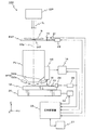
図1には、本発明に係る露光装置の性能情報計測方法及び露光方法の実施に好適な一実施形態に係る露光装置100の概略構成が示されている。この露光装置100は、ステップ・アンド・スキャン方式の走査型投影露光装置、すなわち、いわゆるスキャニング・ステッパである。
FIG. 1 shows a schematic configuration of an
この露光装置100は、照明系IOP、マスクとしてのレチクルRを保持するレチクルステージRST、レチクルステージRSTを駆動するレチクルステージ駆動系29、レチクルRに形成されたパターンの像を感光剤(フォトレジスト)が塗布された物体(及び基板)としてのウエハW上に投影する投影光学系PL、ウエハWを保持して2次元平面(XY平面内)を移動するXYステージ20、XYステージ20を駆動するウエハステージ駆動系22、及びこれらの制御系等を備えている。この制御系は、装置全体を統括制御する主制御装置28を中心として構成されている。
The
前記照明系IOPは、KrFエキシマレーザやArFエキシマレーザなどから成る光源と、オプティカルインテグレータ(フライアイレンズ、内面反射型インテグレータ、又は回折光学素子など)を含む照度均一化光学系、照明視野絞りとしてのレチクルブラインド、リレーレンズ系及びコンデンサレンズ系等(いずれも図示省略)を含む照明光学系とから構成されている。 The illumination system IOP includes a light source composed of a KrF excimer laser, an ArF excimer laser, and the like, and an optical integrator (such as a fly-eye lens, an internal reflection type integrator, or a diffractive optical element). The illumination optical system includes a reticle blind, a relay lens system, a condenser lens system, and the like (all not shown).
照明系IOPによると、光源で発生した露光用のエネルギビームとしての照明光(以下、「照明光IL」と呼ぶ)は、照度均一化光学系により照度分布がほぼ均一な光束に変換される。照度均一化光学系から射出された照明光ILは、リレーレンズ系を介してレチクルブラインドに達する。このレチクルブラインドの開口を通過した光束は、リレーレンズ系、コンデンサレンズ系を通過してレチクルステージRST上に保持されたレチクルR上の矩形スリット状の照明領域IARを均一な照度分布で照明する。 According to the illumination system IOP, illumination light (hereinafter referred to as “illumination light IL”) generated as an energy beam for exposure generated by a light source is converted into a light beam having a substantially uniform illumination distribution by an illumination uniformizing optical system. The illumination light IL emitted from the illuminance uniformizing optical system reaches the reticle blind via the relay lens system. The light beam that has passed through the opening of the reticle blind passes through the relay lens system and the condenser lens system, and illuminates the illumination area IAR having a rectangular slit shape on the reticle R held on the reticle stage RST with a uniform illuminance distribution.
前記レチクルステージRSTは、照明系IOPの図1における下方に配置されている。このレチクルステージRST上には不図示のバキュームチャック等を介してレチクルRが吸着保持されている。レチクルステージRSTは、Y軸方向(図1における紙面左右方向)、X軸方向(図1における紙面直交方向)及びθz方向(XY面に直交するZ軸回りの回転方向)に微小駆動可能であるとともに、所定の走査方向(ここではY軸方向とする)に指定された走査速度で駆動可能となっている。 The reticle stage RST is arranged below the illumination system IOP in FIG. On reticle stage RST, reticle R is held by suction via a vacuum chuck (not shown) or the like. Reticle stage RST can be finely driven in the Y-axis direction (left-right direction in FIG. 1), the X-axis direction (direction orthogonal to the page in FIG. 1), and the θz direction (rotation direction about the Z-axis orthogonal to the XY plane). At the same time, it can be driven at a scanning speed designated in a predetermined scanning direction (here, the Y-axis direction).
レチクルステージRST上にはレチクルレーザ干渉計(以下、「レチクル干渉計」という)21からのレーザビームを反射する移動鏡15が固定されており、レチクルステージRSTの移動面内の位置はレチクル干渉計21によって、例えば0.5〜1nm程度の分解能で常時検出される。ここで、実際には、レチクルステージRST上にはY軸方向に直交する反射面を有する移動鏡とX軸方向に直交する反射面を有する移動鏡とが設けられ、これらの移動鏡に対応してレチクルY干渉計とレチクルX干渉計とが設けられているが、図1ではこれらが代表的に移動鏡15、レチクル干渉計21として示されている。なお、例えば、レチクルステージRSTの端面を鏡面加工して反射面(移動鏡15の反射面に相当)を形成しても良い。また、レチクルステージRSTの走査方向(本実施形態ではY軸方向)の位置検出に用いられるX軸方向に伸びた反射面の代わりに、少なくとも1つのコーナーキューブ型ミラーを用いても良い。ここで、レチクルY干渉計とレチクルX干渉計の一方、例えばレチクルY干渉計は、測長軸を2軸有する2軸干渉計であり、このレチクルY干渉計の計測値に基づきレチクルステージRSTのY位置に加え、θz方向の回転も計測できるようになっている。
A
前記レチクル干渉計21からのレチクルステージRSTの位置情報は主制御装置28に送られ、主制御装置28はこのレチクルステージRSTの位置情報に基づいてレチクルステージ駆動系29を介してレチクルステージRSTを駆動する。
Position information of reticle stage RST from
前記投影光学系PLは、レチクルステージRSTの図1における下方に、その光軸AXpの方向がXY面に直交するZ軸方向となるように配置されている。この投影光学系PLとしては、ここでは両側テレセントリックな縮小系であって、Z軸方向の共通の光軸AXpを有する複数枚のレンズエレメントから成る屈折光学系が用いられている。また、前記レンズエレメントのうちの特定の複数枚は微動可能となっており、主制御装置28からの指令に基づいて、図示しない結像特性補正コントローラによってその移動が制御され、投影光学系PLの結像特性(光学特性の一部)、例えば倍率、ディストーション、コマ収差、及び像面湾曲などを調整できるようになっている。さらに結像特性補正コントローラは、光源の制御パラメータ(印加電圧など)を調整して、光源から発振される露光光ILの波長を所定範囲内でシフトさせることで、投影光学系PLの結像特性を調整することも可能となっている。
The projection optical system PL is arranged below the reticle stage RST in FIG. 1 so that the direction of the optical axis AXp is the Z-axis direction orthogonal to the XY plane. As the projection optical system PL, here is a bilateral telecentric reduction system, and a refractive optical system comprising a plurality of lens elements having a common optical axis AXp in the Z-axis direction is used. Further, a specific plurality of the lens elements can be finely moved, and their movement is controlled by an imaging characteristic correction controller (not shown) based on a command from the
前記XYステージ20は、実際には不図示のベース上をY軸方向に移動するYステージと、このYステージ上をX軸方向に移動するXステージとで構成されているが、図1ではこれらがXYステージ20として示されている。このXYステージ20上に基板ステージとしてのウエハテーブル18が搭載され、このウエハテーブル18上に不図示のウエハホルダを介してウエハWが真空吸着等によって保持されている。
The
XYステージ20は、走査方向(Y軸方向)の移動のみならず、ウエハW上の複数のショット領域を前記照明領域IARと共役な投影光学系PLの視野内の投影領域に位置させることができるように、走査方向に直交する非走査方向(X軸方向)にも移動可能に構成されている。そして、ウエハW上の各ショット領域を走査(スキャン)露光する動作と、次ショットの露光のための走査開始位置(加速開始位置)まで移動する動作とを繰り返すステップ・アンド・スキャン動作を行う。
The
前記ウエハテーブル18は、ウエハWを保持するウエハホルダをZ軸方向及びXY面に対する傾斜方向に微小駆動するものである。このウエハテーブル18の上面には、移動鏡24が設けられており、この移動鏡24にレーザビームを投射して、その反射光を受光することにより、ウエハテーブル18のXY面内の位置を計測するレーザ干渉計26が移動鏡24の反射面に対向して設けられている。なお、実際には、移動鏡はX軸に直交する反射面を有するX移動鏡と、Y軸に直交する反射面を有するY移動鏡とが設けられ、これに対応してレーザ干渉計もX方向位置計測用のXレーザ干渉計とY方向位置計測用のYレーザ干渉計とが設けられているが、図1ではこれらが代表して移動鏡24、レーザ干渉計26として図示されている。なお、例えば、ウエハテーブル18の端面を鏡面加工して反射面(移動鏡24の反射面に相当)を形成しても良い。さらに、例えばボイスコイルモータなどを用いて、ウエハテーブル18をX、Y方向に微動可能、かつXY平面内で微小回転可能に構成しても良い。また、Xレーザ干渉計及びYレーザ干渉計は測長軸を複数有する多軸干渉計であり、ウエハテーブル18のX、Y位置の他、回転(ヨーイング(Z軸回りの回転であるθz回転)、ピッチング(X軸回りの回転であるθx回転)、ローリング(Y軸回りの回転であるθy回転))も計測可能となっている。従って、以下の説明ではレーザ干渉計26によって、ウエハテーブル18のX、Y、θz、θy、θxの5自由度方向の位置が計測されるものとする。なお、このようにして計測されるX座標及びY座標よりなる座標系(X,Y)を、以下ではステージ座標系とも呼ぶ。また、多軸干渉計は45°傾いてウエハテーブル18に設置される反射面を介して、投影光学系PLが載置される架台(不図示)に設置される反射面にレーザビームを照射し、投影光学系PLの光軸方向(Z軸方向)に関する相対位置情報を検出するようにしても良い。
The wafer table 18 finely drives the wafer holder holding the wafer W in the Z-axis direction and the tilt direction with respect to the XY plane. A
レーザ干渉計26の計測値は主制御装置28に供給され、主制御装置28はこのレーザ干渉計26の計測値をモニタしつつ、ウエハステージ駆動系22を介してXYステージ20を駆動することにより、ウエハテーブル18のXY面内の位置制御が行われる。
The measurement value of the
また、ウエハW表面のZ軸方向の位置及び傾斜量は、例えば特開平6−283403号公報等に開示される送光系50a及び受光系50bを有する斜入射方式の多点焦点位置検出系から成るフォーカスセンサAFSによって計測されるようになっている。このフォーカスセンサAFSの計測値も主制御装置28に供給されており、主制御装置28は、フォーカスセンサAFSの計測値に基づいてウエハステージ駆動系22を介してウエハテーブル18をZ軸方向及び傾斜方向(θx,θy方向)に移動し、投影光学系PLの光軸方向に関するウエハWの位置及び傾きを制御するようになっている。
Further, the position and tilt amount of the surface of the wafer W in the Z-axis direction are obtained from an oblique incidence type multi-point focal position detection system having a
また、ウエハテーブル18上には、その表面がウエハWの表面と同じ高さになるように基準板FPが固定されている。この基準板FPの表面には、後述するアライメント検出系のいわゆるベースライン計測等に用いられる基準マークを含む各種の基準マークが形成されている。 Further, a reference plate FP is fixed on the wafer table 18 so that the surface thereof is the same height as the surface of the wafer W. Various reference marks including reference marks used for so-called baseline measurement of an alignment detection system described later are formed on the surface of the reference plate FP.
また、投影光学系PLの鏡筒の側面には、オフ・アクシス方式のアライメント検出系ASが取り付けられている。このアライメント検出系ASとしては、例えば、ハロゲンランプ等を光源とする波長帯域幅の広い光で照明し、CCDカメラなどで撮像したウエハW上のアライメントマーク(又は基準板FP上の基準マーク)の画像データを画像処理してマーク位置を計測するFIA(Field Image Alignment)系のオフアクシス・アライメントセンサが用いられている。なお、アライメント検出系ASは画像処理方式に限られるものではなく、例えばアライメントマークを回折格子とし、コヒーレントビームの照射によって回折格子から発生する同次数の回折光を基準格子に照射し、この基準格子から発生する光を検出する方式などでも良い。 An off-axis alignment detection system AS is attached to the side surface of the projection optical system PL. As this alignment detection system AS, for example, an alignment mark on the wafer W (or a reference mark on the reference plate FP) that is illuminated with light having a wide wavelength bandwidth using a halogen lamp or the like as a light source and captured by a CCD camera or the like. An FIA (Field Image Alignment) type off-axis alignment sensor that measures image data by image processing is used. The alignment detection system AS is not limited to the image processing method. For example, the alignment mark is a diffraction grating, and the reference grating is irradiated with the same-order diffracted light generated from the diffraction grating by the irradiation of the coherent beam. A method of detecting light generated from the light source may be used.
アライメント制御装置16は、アライメント検出系ASからの情報をA/D変換するとともに、レーザ干渉計26の計測値を参照してマーク位置を検出する。この検出結果はアライメント制御装置16から主制御装置28に供給されるようになっている。
The alignment control device 16 A / D converts information from the alignment detection system AS, and detects a mark position with reference to a measurement value of the
さらに、本実施形態の露光装置100では、図示は省略されているが、レチクルRの上方に、例えば特開平7−176468号公報等に開示される、投影光学系PLを介してレチクルR上のレチクルマーク又はレチクルステージRST上の基準マーク(共に図示省略)と基準板FP上のマークとを同時に観察するための露光波長を用いたTTR(Through The Reticle)アライメント系から成る一対のレチクルアライメント顕微鏡が設けられている。これらのレチクルアライメント顕微鏡の検出信号は、アライメント制御装置16を介して主制御装置28に供給されるようになっている。
Further, in the
主制御装置28は、CPU(中央演算処理装置)、メモリ(ROM、RAM)、各種インターフェース等からなるいわゆるマイクロコンピュータ(又はワークステーション)を含んで構成され、露光動作が的確に行われるように、例えば、レチクルRとウエハWの同期走査、ウエハWのステッピング、露光タイミング等を統括して制御する。また、主制御装置28は、記憶装置27と接続されており、記憶装置27に対して各種データの保存や読み出しができるようになっている。
The
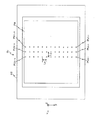
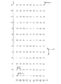
図2には、露光装置100の性能の一つである投影光学系PLの光学特性を計測するのに用いられるテスト用レチクルRT(以下、「レチクルRT」と略述する)の一例が示されている。このレチクルRTは、ガラス基板42の一方の面(図1のレチクルステージRSTに搭載されたときに下面となる面)の中央にパターン領域PAが形成され、パターン領域PAのX軸方向の両側には、少なくとも1対のレチクルアライメントマーク(図示省略)が形成されている。
FIG. 2 shows an example of a test reticle R T (hereinafter abbreviated as “reticle R T ”) used to measure the optical characteristics of the projection optical system PL, which is one of the performances of the
前記パターン領域PA内には、一例として図2に示されるように、39(13×3)個の同一の計測用パターンとしてのテストパターンが形成されており、それらはY軸方向に3個、X軸方向に13個がマトリックス状に2次元配置されている。そこで、テストパターンを特定するために、配列PUi,j(i=1〜3、j=1〜13)という表記を用いることとする。ここで、添え字iはY軸方向に関するテストパターンの配列番号を示し、図2の紙面左側(+Y側)に向かってその値は増加するものとする。添え字jはX軸方向に関するテストパターンの配列番号を示し、紙面上側(−X側)に向かってその値は増加するものとする。なお、テストパターンPUi,jは、39個全てが同時にレチクルRT上の照明領域IAR内に含まれるように配置されている。そして、X軸方向に関するテストパターン間の距離をLx(例えば2mm)、Y軸方向に関するテストパターン間の距離をLy(例えば3mm)とする。さらに、以下においては、適宜、PU1,1〜PU1,13を「第1パターンユニット」、PU2,1〜PU2,13を「第2パターンユニット」、PU3,1〜PU3,13を「第3パターンユニット」という。また、パターン領域PA内のテストパターンPUi,jが配置されていない領域は遮光領域となっている。 As shown in FIG. 2 as an example, 39 (13 × 3) test patterns as the same measurement pattern are formed in the pattern area PA, and these are three in the Y-axis direction. Thirteen in the X-axis direction are two-dimensionally arranged in a matrix. Therefore, in order to specify the test pattern, the notation of the array PU i, j (i = 1 to 3, j = 1 to 13) is used. Here, the subscript i indicates the array number of the test pattern in the Y-axis direction, and its value increases toward the left side (+ Y side) of FIG. The subscript j indicates the array number of the test pattern in the X-axis direction, and its value increases toward the upper side (−X side) of the drawing. Note that all 39 test patterns PU i, j are arranged so as to be simultaneously included in the illumination area IAR on the reticle RT . A distance between test patterns in the X-axis direction is Lx (for example, 2 mm), and a distance between test patterns in the Y-axis direction is Ly (for example, 3 mm). Further, in the following, PU 1,1 to PU 1,13 will be referred to as “first pattern unit”, PU 2,1 to PU 2,13 as “second pattern unit”, PU 3,1 to PU 3, as appropriate . 13 is referred to as a “third pattern unit”. In addition, a region where the test pattern PU i, j is not arranged in the pattern region PA is a light shielding region.
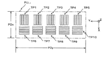
テストパターンPUi,jは、一例として図3に示されるように、10種類のラインアンドスペース(以下、「L/S」と略述する)パターンTP1〜TP10を含んでいる。L/SパターンTP1〜TP10のそれぞれは、5本のラインパターンが周期的に配置されている。なお、本明細書においては、ライン部の幅とスペース部の幅との比が1:1(すなわち、デューティ比が50パーセント)のもののみでなく、ラインパターンが所定ピッチで所定方向に並んでいるマルチラインパターンの全てを、L/Sパターンと便宜上呼ぶものとする。 As an example , the test pattern PU i, j includes ten types of line and space (hereinafter abbreviated as “L / S”) patterns TP1 to TP10, as shown in FIG. In each of the L / S patterns TP1 to TP10, five line patterns are periodically arranged. In the present specification, not only the ratio of the width of the line portion to the width of the space portion is 1: 1 (that is, the duty ratio is 50%), but the line patterns are arranged in a predetermined direction at a predetermined pitch. All the multiline patterns are referred to as L / S patterns for convenience.
L/SパターンTP1〜TP5では、各ラインパターンはX軸方向に伸びY軸方向を周期方向として配置されており、L/SパターンTP6〜TP10では、各ラインパターンはY軸方向に伸びX軸方向を周期方向として配置されている。 In the L / S patterns TP1 to TP5, each line pattern extends in the X-axis direction and is arranged with the Y-axis direction as a periodic direction. In the L / S patterns TP6 to TP10, each line pattern extends in the Y-axis direction. The directions are arranged as periodic directions.
本実施形態では、一例として、L/SパターンTP1及びTP6では、ラインパターンの線幅は200nmであり、L/SパターンTP2及びTP7では、ラインパターンの線幅は180nmであり、L/SパターンTP3及びTP8では、ラインパターンの線幅は150nmであり、L/SパターンTP4及びTP9では、ラインパターンの線幅は140nmであり、L/SパターンTP5及びTP10では、ラインパターンの線幅は120nmであるものとする。なお、L/SパターンTP1〜TP10のそれぞれは、同一のピッチを有している。従って、これらのL/SパターンTP1〜TP10は、線幅に応じたデューティ比をそれぞれ有している。また、図3に示されるように、テストパターンPUi,jのY軸方向の長さをPDy、X軸方向の長さをPDxとする。この長さPDx,PDyにより規定される領域PUi,jが転写パターンと言うことになるが、後述するウエハ上での転写領域WU(1つの転写パターンがウエハ上で転写される領域)をなるべく小さくするために、この長さPDx,PDyは充分に小さく設定されている。 In this embodiment, as an example, the line width of the line pattern is 200 nm in the L / S patterns TP1 and TP6, and the line width of the line pattern is 180 nm in the L / S patterns TP2 and TP7. In TP3 and TP8, the line width of the line pattern is 150 nm, in L / S patterns TP4 and TP9, the line width of the line pattern is 140 nm, and in L / S patterns TP5 and TP10, the line width of the line pattern is 120 nm. Suppose that Each of the L / S patterns TP1 to TP10 has the same pitch. Therefore, these L / S patterns TP1 to TP10 each have a duty ratio corresponding to the line width. Further, as shown in FIG. 3, the length in the Y-axis direction of the test pattern PU i, j is PDy, and the length in the X-axis direction is PDx. The area PU i, j defined by the lengths PDx and PDy is referred to as a transfer pattern. A transfer area WU on the wafer (an area where one transfer pattern is transferred on the wafer) to be described later is as much as possible. In order to reduce the length, the lengths PDx and PDy are set sufficiently small.
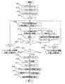
次に、本実施形態の露光装置100によりレチクルパターンをテスト用ウエハWT(物体、以下、「ウエハWT」と略述する)上に転写して投影光学系PLの光学特性の1つである像面湾曲を計測するための処理動作について、図4のフローチャートを用いて説明する。図4のフローチャートは、主制御装置28のCPUによって実行される一連の処理アルゴリズムに対応している。
Next, the reticle pattern is transferred onto a test wafer W T (object, hereinafter abbreviated as “wafer W T ”) by the
図4のステップ401では、不図示のレチクルローダを用いてレチクルステージRST上にレチクルRTをロードする。 In step 401 of FIG. 4, reticle RT is loaded onto reticle stage RST using a reticle loader (not shown).
次のステップ403では、不図示のウエハローダを用いてウエハWTをウエハテーブル18上にロードする。
In the
次のステップ405では、例えば、前述のレチクルアライメント顕微鏡(不図示)により投影光学系PLを介して少なくとも一対のレチクルアライメントマークとこれに対応して基準板FPの表面に形成されている少なくとも一対の基準マークとの相対位置を検出する。そして、そのときのレチクル干渉計21及びレーザ干渉計26の測定値とから、レチクル干渉計21の測長軸によって規定されるレチクルステージ座標系と、レーザ干渉計26の測長軸によって規定されるウエハステージ座標系との関係を求める。すなわち、このようにして、レチクルアライメントを行なう。
In the
次のステップ407では、ウエハWT上におけるテストパターンPUi,jの転写領域を区別するためのフラグFに0をセットする。
In the
次のステップ409では、ウエハWTのフォーカス位置の目標値を初期化する。すなわち、ウエハWTのフォーカス位置の目標値にZ1を設定する。なお、本実施形態では、一例としてウエハWTのフォーカス位置ZmをZ1からΔZ刻みでZ9まで変化させる。
In the
次のステップ411では、ウエハWTのフォーカス位置が目標値(この場合Z1)と一致するように、フォーカスセンサAFSからの計測値をモニタしながらウエハステージ駆動系22を介してウエハテーブル18をZ軸方向に微少駆動する。但し、ここでは、ウエハWTの露光面の傾きを補正するためにウエハテーブル18をX軸回り及びY軸回りに回転する、いわゆるレベリング機能は動作させない。この理由については後述する。
In the
次のステップ413では、この状態で露光を行なう。なお、ここでは、投影光学系PLの像面湾曲を計測するのが目的であるために、露光中はレチクルRTとウエハWT、すなわちレチクルステージRSTとXYステージ20は、静止させたままである。これにより、レチクルRTのパターンが投影光学系PLを介してウエハWT上に縮小転写される。すなわち、本実施形態では、39個のテストパターンPUi,jの転写像(潜像)が、ウエハWT上に形成される。
In the
次のステップ415では、ウエハWTのフォーカス位置の目標値がZ9であるか否かを判断する。ここでは、最初の目標値Z1での露光が終了しただけであるため、ステップ415での判断は否定されステップ417に移行する。
In the
このステップ417では、ウエハWTのフォーカス位置の目標値にΔZを加算する。
In
次のステップ419では、レーザ干渉計26の計測値をモニタしつつウエハステージ駆動系22を介してXYステージ20を移動し、ウエハWTを−Y方向に次の(1)式で示される距離ΔY1だけシフトする。そして、前記ステップ411に戻る。
In the
ΔY1=2・PDy・β……(1) ΔY1 = 2 ・ PDy ・ β …… (1)
上記(1)式におけるβは投影光学系PLの投影倍率である。 In the above equation (1), β is the projection magnification of the projection optical system PL.
以下、ステップ415での判断が肯定されるまで、ステップ411→413→415→417→419の処理、判断を繰り返す。
Thereafter, the processes and determinations in
ステップ415では、そのとき設定されているウエハWTのフォーカス位置の目標値がZ9であれば、ここでの判断は肯定され、ステップ421に移行する。
In
ステップ415での判断が肯定されたときに、ウエハWT上に形成されているテストパターンの転写領域(第1の領域)の一例が図5に示されている。なお、図5には、便宜上、第2パターンユニットの転写領域のみが示されている。ここで、フォーカス位置の目標値がZmのときのテストパターンPUi,jの転写領域(部分領域)をWUf,m,i,jと表記する。添え字fはフラグFの値(この場合は0)を意味している。従って、図5における紙面左下の転写領域は、WU0,1,2,1であり、図5における紙面右上の転写領域は、WU0,9,2,13である。すなわち、WU0,1,2,1〜WU0,9,2,13の117(=13×9)個の転写領域が形成されている。なお、ウエハWT上には、第1パターンユニットが転写された領域WU0,1,1,1〜WU0,9,1,13及び第3パターンユニットが転写された領域WU0,1,3,1〜WU0,9,3,13(いずれも不図示)も同様に形成されている。
When the determination in
図4に戻り、次のステップ421では、フラグFの値に応じて分岐先を判断する。ここでは、F=0なのでステップ423へ分岐する。
Returning to FIG. 4, in the
このステップ423では、ウエハWTを所定の目標位置(以下、便宜上「第1の目標位置」と呼ぶ)に位置決めするため、XYステージ20をXY面内で移動する。例えば、以下の手順でXYステージ20を移動する。
In
すなわち、先ずウエハWTを最初の位置に戻すために、ウエハWTが距離(ΔY1×8)だけ+Y方向にシフトするようにXYステージ20を移動する。次に、ウエハWTが次の(2)式で算出される距離WLxだけ+X方向にシフトするようにXYステージ20を移動する(図6参照)。なお、(2)式において、Lxは、X軸方向に隣り合うテストパターン間のX軸方向に関する距離である(図2参照)。
That is, first, in order to return the wafer W T to the initial position, the
WLx=β・Lx ……(2) WLx = β ・ Lx (2)
さらに、ウエハWTが次の(3)式で示される距離ΔY2だけ−Y方向にシフトするようにXYステージ20を移動する(図6参照)。
Further, the wafer W T to move the
ΔY2=PDy・β ……(3) ΔY2 = PDy · β (3)
この結果、ウエハは、ステップ423における移動開始前の位置からX軸方向に関して+WLx、Y軸方向に関して(8ΔY1−ΔY2)だけシフトした第1の目標位置、すなわち、最初の位置から+X方向にWLx、−Y方向にΔY2だけシフトした位置に位置決めされる。勿論、上記の3段階の手順で移動する必要はなく、ステップ423における移動開始前の位置から上記の第1の目標位置に向かって直線的にXYステージ20を移動しても良い。
As a result, the wafer has a first target position shifted by + WLx with respect to the X-axis direction and (8ΔY1−ΔY2) with respect to the Y-axis direction from the position before the movement start in
次のステップ425では、フラグFの値を1に変更した後、ステップ409に戻る。
In the
このステップ409では、ウエハWTのフォーカス位置の目標値を初期化する。すなわち、目標値にZ1を設定する。
In
以下、ステップ415での判断が肯定されるまで、ステップ411→413→415→417→419の処理、判断を繰り返す。
Thereafter, the processes and determinations in
ステップ415での判断が肯定されると、ステップ421に移行する。
If the determination in
ステップ415での判断が肯定されたときに、ウエハWT上に形成されているテストパターンの転写領域の一例が図6に示されている。なお、図6には、便宜上、ウエハWT上の図5と同じ場所が示されており、図6中の斜線で示される転写領域は、F=1のときに第2パターンユニットが転写された領域(第2の領域の一部)WU1,1,2,1〜WU1,9,2,13である。例えば、図6における紙面左下の斜線で示される転写領域はWU1,1,2,1であり、図6における紙面右上の斜線で示される転写領域はWU1,9,2,13である。なお、図6中の白抜きで示される転写領域は、前述したF=0のときの転写領域WU0,1,2,1〜WU0,9,2,13である。また、ウエハWT上には、F=1のときに第1パターンユニットが転写された領域(第2の領域の一部)WU1,1,1,1〜WU1,9,1,13及び第3パターンユニットが転写された領域(第2の領域の一部)WU1,1,3,1〜WU1,9,3,13(いずれも不図示)も同様に形成されている。
When the determination in
ステップ421では、F=1であるのでステップ429に分岐する。
In
このステップ429では、ウエハWTを次の目標位置(以下、便宜上「第2の目標位置」と呼ぶ)に位置決めするため、XYステージ20をXY面内で移動する。例えば、以下の手順でXYステージ20を移動する。
In
すなわち、先ずウエハWTを最初の位置に戻すために、ウエハWTが距離(ΔY1×8+ΔY2)だけ+Y方向に、距離WLxだけ−X方向にシフトするようにXYステージ20を移動する。次いで、ウエハWTが次の(4)式で算出される距離WLyだけ−Y方向にシフトするようにXYステージ20を移動する。ここで、LyはY軸方向に隣り合うテストパターン間のY軸方向に関する距離である(図2参照)。
That is, first, in order to return the wafer W T to the initial position, the
WLy=β・Ly ……(4) WLy = β ・ Ly (4)
さらに、ウエハWTが次の(5)式で算出される距離ΔX1だけ+X方向にシフトするようにXYステージ20を移動する。
Further, the
ΔX1=PDx・β ……(5) ΔX1 = PDx · β (5)
この結果、ウエハは、ステップ429における移動開始前の位置からX軸方向に関して(−WLx+ΔX1)、Y軸方向に関して(8×ΔY1+ΔY2−WLy)だけシフトした第2の目標位置、すなわち、最初の位置から+X方向にΔX1、−Y方向にWLyだけシフトした位置に位置決めされる。勿論、上記の3段階の手順で移動する必要はなく、ステップ429における移動開始前の位置から上記の第2の目標位置に向かって直線的にXYステージ20を移動しても良い。
As a result, the wafer is shifted from the position before the start of movement in
次のステップ431では、フラグFの値を2に変更した後、ステップ409に戻る。
In the
このステップ409では、ウエハWTのフォーカス位置の目標値を初期化する。すなわち目標値にZ1を設定する。
In
以下、ステップ415での判断が肯定されるまで、ステップ411→413→415→417→419の処理、判断を繰り返す。
Thereafter, the processes and determinations in
図4のステップ415での判断が肯定されると、ステップ421に移行する。
If the determination at
ステップ415での判断が肯定されたときに、ウエハWT上に形成されているテストパターンの転写領域の一例が図7に示されている。なお、図7には、便宜上、ウエハWT上の図6と同じ場所が示されており、図7中のダブルハッチングで示される領域はF=2のときに第1パターンユニットが転写された領域WU2,1,1,1〜WU2,9,1,13である。例えば、図7における紙面左下のダブルハッチング領域はWU2,1,1,1であり、図7における紙面右上のダブルハッチング領域はWU2,9,1,13である。なお、図7中の斜線で示される転写領域は、前述したF=1のときの転写領域WU1,1,2,1〜WU1,9,2,13であり、図7中の白抜きで示される転写領域は、前述したF=0のときの転写領域WU0,1,2,1〜WU0,9,2,13である。また、ウエハWT上には、F=2のときに第2パターンユニットが転写された領域WU2,1,2,1〜WU2,9,2,13及び第3パターンユニットが転写された領域WU3,1,3,1〜WU3,9,3,13(いずれも不図示)も同様に形成されている。
When the determination in
ここで、各転写領域WUf,m,i,jは非常に小さいので、図7に示されるように、転写領域WU0,m,2,1及びWU2,m,1,1(m=1〜9)のX座標値をX1、転写領域WU0,m,2,2、WU1,m,2,1及びWU2,m,1,2(m=1〜9)のX座標値をX2、転写領域WU0,m,2,3、WU1,m,2,2及びWU2,m,1,3(m=1〜9)のX座標値をX3、……、転写領域WU0,m,2,13、WU1,m,2,12及びWU2,m,1,13(m=1〜9)のX座標値をX13、転写領域WU1,m,2,13(m=1〜9)のX座標値をX14とする。
Here, since each transfer area WU f, m, i, j is very small, as shown in FIG. 7, the transfer areas WU 0, m, 2,1 and WU 2, m, 1,1 (m = X 1 and X coordinate values of 1-9), a
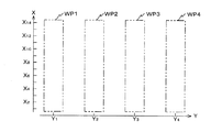
また、本実施形態では、ウエハWT上におけるテストパターンの転写領域は、一例として図8に示されるように、4つのグループ(WP1、WP2、WP3、WP4)に大別することができる。グループWP1には、F=0及びF=1での第1パターンユニットの転写領域が含まれる。グループWP2には、F=0及びF=1での第2パターンユニットの転写領域とF=2での第1パターンユニットの転写領域とが含まれる(図7参照)。グループWP3には、F=0及びF=1での第3パターンユニットの転写領域とF=2での第2パターンユニットの転写領域とが含まれる。グループWP4には、F=2での第3パターンユニットの転写領域が含まれる。そして、グループWP1の中心のY座標値をY1、グループWP2の中心のY座標値をY2、グループWP3の中心のY座標値をY3、グループWP4の中心のY座標値をY4とする。ここで、転写領域WUf,m,i,jは非常に小さいため、便宜上、グループWP1の各転写領域のY座標値はすべて同一、すなわちY1とみなすこととする。同様にグループWP2の各転写領域のY座標値はすべてY2、グループWP3の各転写領域のY座標値はすべてY3、グループWP4の各転写領域のY座標値はすべてY4とみなすこととする。なお、図8では、便宜上、転写領域WUf,m,i,jの図示は省略している。 Further, in the present embodiment, the transfer area of the test pattern on the wafer W T, as shown in FIG. 8 as an example, can be roughly divided into four groups (WP1, WP2, WP3, WP4 ). The group WP1 includes the transfer area of the first pattern unit at F = 0 and F = 1. The group WP2 includes a transfer area of the second pattern unit at F = 0 and F = 1 and a transfer area of the first pattern unit at F = 2 (see FIG. 7). The group WP3 includes a transfer area of the third pattern unit at F = 0 and F = 1 and a transfer area of the second pattern unit at F = 2. Group WP4 includes a transfer area of the third pattern unit at F = 2. The Y coordinate value of the center of the group WP1 is Y 1 , the Y coordinate value of the center of the group WP2 is Y 2 , the Y coordinate value of the center of the group WP3 is Y 3 , and the Y coordinate value of the center of the group WP4 is Y 4 . To do. Here, since the transfer area WU f, m, i, j is very small, for convenience, the Y coordinate values of the transfer areas of the group WP1 are all considered to be the same, that is, Y 1 . Similarly, it is assumed that the Y coordinate values of the transfer areas of the group WP2 are all Y 2 , the Y coordinate values of the transfer areas of the group WP3 are all Y 3 , and the Y coordinate values of the transfer areas of the group WP4 are all Y 4. To do. In FIG. 8, the transfer region WU f, m, i, j is not shown for convenience.
そこで、本実施形態では、座標値(Xp、Yq)(p=1〜14、q=1〜4)で示されるウエハWT上の各位置を計測点とする。 Therefore, in the present embodiment, each position on the wafer W T indicated by the coordinate values (X p , Y q ) (p = 1 to 14, q = 1 to 4) is set as a measurement point.
図4に戻り、次のステップ421では、F=2であるのでステップ433に分岐する。
Returning to FIG. 4, in the
このステップ433では、不図示のウエハアンローダを介してウエハWTをウエハテーブル18上からアンロードした後、不図示のウエハ搬送系により、ウエハWTを露光装置100にインラインにて接続されている不図示のコータ・デベロッパに搬送する。
In
次のステップ435では、図示しないコータ・デベロッパの制御系にウエハWTの現像を指示する。これによって、コータ・デベロッパにてウエハWTの現像が行なわれる。コータ・デベロッパでの現像の終了により、ウエハWT上の転写領域WUf,m,i,j毎に、L/SパターンTP1〜TP10それぞれのレジスト像が形成される。
In the
そして、ウエハWTの現像が終了したことを、不図示のコータ・デベロッパの制御系からの通知により確認すると、アライメント検出系ASを用いてレジスト像の線幅計測を行なうため、ステップ437に移行して、不図示のウエハローダに指示し、ウエハWTをウエハテーブル18上に再度ロードする。そして、ステップ439のウエハWTの表面形状情報を算出するサブルーチンに移行する。
Then, that developing the wafer W T is completed, confirms the notification from the control system of the coater developer (not shown) for performing line width measurement of the resist image by using the alignment detection system AS, proceeds to step 437 and instructs the wafer loader (not shown), again loads the wafer W T on the wafer table 18. Then, the process proceeds to the subroutine for calculating the surface shape information of the wafer W T in
このステップ439のサブルーチンでは、まず、図9のステップ501において、ウエハWT上に形成されたレジスト像を、アライメント検出系ASを用いて順次撮像し、その撮像データに基づいて所定の画像処理を行ない、転写領域WUf,m,i,j毎に、L/SパターンTP1〜TP10それぞれのレジスト像の線幅を計測する。なお、ここではコマ収差の影響を除くために5本のラインパターンのうち、周期方向に関して中央部に配置されたラインパターンのレジスト像の線幅を計測する。
In the subroutine of
次のステップ505では、Y座標値がY2でのX軸方向に関するウエハWTの表面形状情報を算出するために、グループWP2に含まれる各レジスト像の線幅値に基づいて各計測点での最良フォーカス位置を、一例として以下の手順で求める。なお、計測点(Xp、Yq)での最良フォーカス位置をBf,p,qと表記する。添え字fはフラグFの値を意味している。
In the
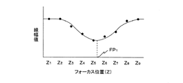
すなわち、先ず、計測点(X1、Y2)における最良フォーカス位置を求める。ここでは、F=0のときにテストパターンPU2,1が転写された9個の転写領域(WU0,1,2,1、WU0,2,2,1、WU0,3,2,1、・・・・・・、WU0,9,2,1)において計測された各レジスト像の線幅値に基づいて、一例として図10に示されるように、L/SパターンTP1のレジスト像の線幅値とフォーカス位置Zとの相関関係を示す近似曲線を求め、該近似曲線の極値FP1を求める。さらに、L/SパターンTP2〜TP10のレジスト像についても、それぞれ線幅値とフォーカス位置との相関関係を示す近似曲線を求め、各近似曲線の極値FP2〜FP10を求める。そして、上記の如くして得られた10個の極値FP1〜FP10を統計処理(例えば、平均化)し、その結果を最良フォーカス位置B0,1,2とする。 That is, first, the best focus position at the measurement point (X 1 , Y 2 ) is obtained. Here, nine transfer areas (WU 0,1,2,1 , WU 0,2,2,1 , WU 0,3,2,2 ) to which the test pattern PU 2,1 has been transferred when F = 0 . 1 ,..., Based on the line width value of each resist image measured in WU 0,9,2,1 ), as shown in FIG. 10 as an example, the resist of the L / S pattern TP1 An approximate curve indicating the correlation between the line width value of the image and the focus position Z is obtained, and an extreme value FP 1 of the approximate curve is obtained. Further, with respect to the resist images of the L / S patterns TP2 to TP10, approximate curves indicating the correlation between the line width value and the focus position are obtained, and extreme values FP 2 to FP 10 of the approximate curves are obtained. Then, the statistical processing ten extrema FP 1 ~FP 10 obtained as described above (e.g., averaged), and the result with the best focus position B 0, 1, 2.
次に、計測点(X2、Y2)における最良フォーカス位置を求める。ここでは、F=0のときにテストパターンPU2,2が転写された9個の転写領域(WU0,1,2,2、WU0,2,2,2、WU0,3,2,2、……、WU0,9,2,2)において計測された各レジスト像の線幅値に基づいて、上記と同様にして最良フォーカス位置B0,2,2を求める。さらに、F=1のときにテストパターンPU2,1が転写された9個の転写領域(WU1,1,2,1、WU1,2,2,1、WU1,3,2,1、……、WU1,9,2,1)において計測された各レジスト像の線幅値に基づいて、上記と同様にして最良フォーカス位置B1,2,2を求める。 Next, the best focus position at the measurement point (X 2 , Y 2 ) is obtained. Here, nine transfer regions (WU 0,1,2,2 , WU 0,2,2,2 , WU 0,3,2,2 ) to which the test pattern PU 2,2 is transferred when F = 0 are set. 2 ,..., The best focus position B 0,2,2 is obtained in the same manner as described above based on the line width value of each resist image measured in WU 0,9,2,2 ). Further, nine transfer regions (WU 1,1,2,1 , WU 1,2,2,1 , WU 1,3,2,1 to which the test pattern PU 2,1 is transferred when F = 1 are set. ,..., The best focus position B 1,2,2 is obtained in the same manner as described above based on the line width value of each resist image measured in WU 1,9,2,1 ).
以下、同様にして他の計測点(Xp、Y2)(p=3〜14)における最良フォーカス位置を求める。 Hereinafter, similarly, the best focus position at other measurement points (X p , Y 2 ) (p = 3 to 14) is obtained.
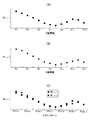
本実施形態では、一例として図11(A)に示されるように、計測点(X1、Y2)〜(X13、Y2)において、F=0のときに転写されたテストパターンのレジスト像の線幅値に基づいて第1の最良フォーカス位置(第1のフォーカス情報)が得られ、一例として図11(B)に示されるように、計測点(X2、Y2)〜(X14、Y2)において、F=1のときに転写されたテストパターンのレジスト像の線幅値に基づいて第2の最良フォーカス位置(第2のフォーカス情報)が得られる。 In this embodiment, as shown in FIG. 11A as an example, the test pattern resist transferred when F = 0 at the measurement points (X 1 , Y 2 ) to (X 13 , Y 2 ). A first best focus position (first focus information) is obtained based on the line width value of the image. As an example, as shown in FIG. 11B, measurement points (X 2 , Y 2 ) to (X 14 , Y 2 ), the second best focus position (second focus information) is obtained based on the line width value of the resist image of the test pattern transferred when F = 1.
従来は、各計測点での最良フォーカス位置を統計処理(例えば、最小自乗法)して像面湾曲を求めていた。しかしながら、一例として図11(C)に示されるように、同一のテストパターンに由来する最良フォーカス位置であっても、第1の最良フォーカス位置と第2の最良フォーカス位置とは必ずしも一致していない。これは、ウエハWTの表面形状が平坦ではないことに起因している。 Conventionally, the field curvature is obtained by performing statistical processing (for example, the method of least squares) on the best focus position at each measurement point. However, as shown in FIG. 11C as an example, even if the best focus position is derived from the same test pattern, the first best focus position and the second best focus position do not necessarily match. . This surface shape of the wafer W T is due to not flat.
ここで、最良フォーカス位置の計測結果とウエハWTの表面形状との関係について考察する。 Here, consider the relationship between the surface shape of the measurement result of the best focus position and the wafer W T.
先ず、ここでウエハWT上の計測点(Xp、Yq)のZ軸方向に関する所定の基準位置からの距離(以下、便宜上「Z高さ」という)をDzp,qとする。また、ウエハWTの表面が平坦であると仮定したときにテストパターンPUi,jの転写像に基づいて得られる仮想的な最良フォーカス位置をHi,jとする。 First, here, a distance (hereinafter, referred to as “Z height” for convenience) of a measurement point (X p , Y q ) on the wafer W T from a predetermined reference position in the Z-axis direction is defined as Dz p, q . Further, assume that the virtual best focus position obtained based on the transfer image of the test pattern PU i, j when the surface of the wafer W T is flat is H i, j .
そこで、例えば、計測点(X1、Y2)に転写されたテストパターンPU2,1の転写像に基づいて得られる第1の最良フォーカス位置B0,1,2は、次の(6)式で示されるように、仮想的な最良フォーカス位置H2,1とZ高さDz1,2とが加算されたものであると考えることができる。 Therefore, for example, the first best focus position B 0,1,2 obtained based on the transferred image of the test pattern PU 2,1 transferred to the measurement point (X 1 , Y 2 ) is the following (6). As shown in the equation, it can be considered that the virtual best focus position H 2,1 and the Z height Dz 1,2 are added.
B0,1,2=H2,1+Dz1,2 ……(6) B 0,1,2 = H 2,1 + Dz 1,2 (6)
また、例えば、計測点(X2、Y2)に転写されたテストパターンPU2,1の転写像に基づいて得られる第2の最良フォーカス位置B1,2,2は、次の(7)式で示されるように、仮想的な最良フォーカス位置H2,1とZ高さDz2,2とが加算されたものであると考えることができる。 Further, for example, the second best focus position B 1,2,2 obtained based on the transferred image of the test pattern PU 2,1 transferred to the measurement point (X 2 , Y 2 ) is the following (7) As shown by the equation, it can be considered that the virtual best focus position H 2,1 and the Z height Dz 2,2 are added.
B1,2,2=H2,1+Dz2,2 ……(7) B 1,2,2 = H 2,1 + Dz 2,2 (7)
次に、上記(7)式と(6)式の差を求めると、次の(8)式が得られる。 Next, when the difference between the above equations (7) and (6) is obtained, the following equation (8) is obtained.
B1,2,2-B0,1,2=Dz2,2-Dz1,2 ……(8) B 1,2,2 -B 0,1,2 = Dz 2,2 -Dz 1,2 (8)
上記(8)式から明らかなように、第2の最良フォーカス位置B1,2,2と第1の最良フォーカス位置B0,1,2との差は、テストパターンPU2,1が転写された2つの計測点(X2、Y2)と(X1、Y2)のZ高さの差を意味している。すなわち、同一のテストパターンがウエハWT上の異なる計測点に転写された場合、各計測点で得られる最良フォーカス位置の差は、Z高さの差を示している。 As apparent from the above equation (8), the difference between the second best focus position B 1,2,2 and the first best focus position B 0,1,2 is that the test pattern PU 2,1 is transferred. It means the difference in Z height between the two measurement points (X 2 , Y 2 ) and (X 1 , Y 2 ). That is, when the same test pattern was transferred to the different measuring points on the wafer W T, the difference between the best focus position obtained at each measurement point indicates the difference between the Z height.
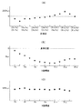
図9に戻り、ステップ507では、上記考察に基づき、X軸方向に関して隣り合う2つの計測点(Xp、Y2)と(Xp+1、Y2)のZ高さの差を求めるために、同一のテストパターンに由来する2つの最良フォーカス位置、すなわち、第2の最良フォーカス位置B1,p+1,2と第1の最良フォーカス位置B0,p,2との差(以下、「第1のフォーカス差」という)ΔDXp,2(p=1〜13)を、次の(9)式を用いて算出する。
Returning to FIG. 9, in
ΔDXp,2=B1,p+1,2-B0,p,2 ……(9)
ここで算出された第1のフォーカス差ΔDXp,2の一例が図12(A)に示されている。この図12(A)において、例えば、ΔDX5,2は、計測点(X6、Y2)と(X5、Y2)のZ高さの差を示している。
ΔDX p, 2 = B 1, p + 1,2 -B 0, p, 2 (9)
An example of the first focus difference ΔDX p, 2 calculated here is shown in FIG. In FIG. 12A, for example, ΔDX 5,2 indicates a difference in Z height between measurement points (X 6 , Y 2 ) and (X 5 , Y 2 ).
図9に戻り、次のステップ509では、一例として計測点(X1、Y2)におけるZ軸方向の位置を基準位置とし、次の(10)式に示されるように、第1のフォーカス差ΔDXp,2を順次積算して、計測点(Xp、Y2)(p=2〜14)におけるZ高さDp,2を求める。なお、計測点(X1、Y2)を基準位置としているため、D1,2=0である。
Returning to FIG. 9, in the
Dp,2=Dp-1,2+ΔDXp-1,2 ……(10)
ここで、算出されたZ高さDp,2は、一例として、図12(B)に示されるように、X軸方向(但し、Y=Y2)に関するウエハWTの相対的な表面形状を示している。
D p, 2 = D p-1,2 + ΔDX p-1,2 (10)
Here, Z height D p, 2, which is calculated, as an example, as illustrated in FIG. 12 (B), X-axis direction (where, Y = Y 2) relative surface shape about the wafer W T Is shown.
次のステップ511では、前記と同様にして、グループWP1及びWP3における第1の最良フォーカス位置B0,p,1及びB0,p,3(p=1〜13)を求める。また、F=2のときに転写されたテストパターンのレジスト像の線幅値に基づいて第3の最良フォーカス位置B2,p,q(p=1〜13、q=2〜4)を求める。
In the
次のステップ513では、Y軸方向に隣り合う2つの計測点(Xp、Yq+1)と(Xp、Yq)のZ高さの差を求めるために、第3の最良フォーカス位置B2,p,q+1と第1の最良フォーカス位置B0,p,qの差(以下、「第2のフォーカス差」という)ΔDYp,q(p=1〜13、q=1〜3)を、次の(11)式を用いて算出する。
In the
ΔDYp,q=B2,p,q+1-B0,p,q ……(11) ΔDY p, q = B 2, p, q + 1 -B 0, p, q ...... (11)
そして、次のステップ515では、上記の如く計測点(Xp、Y2)におけるZ高さDp,2(p=1〜13)が、すでに求められているので、次の(12)式に示されるように、Z高さDp,2から第2のフォーカス差ΔDYp,1を減算することにより、計測点(Xp、Y1)におけるZ高さDp,1(p=1〜13)を求めることができる。
In the
Dp,1=Dp,2-ΔDYp,1 ……(12) D p, 1 = D p, 2 -ΔDY p, 1 (12)
また、同様に、次の(13)式に示されるように、Z高さDp,2に第2のフォーカス差ΔDYp,2を加算することにより、計測点(Xp、Y3)におけるZ高さDp,3(p=1〜13)を求めることができる。 Similarly, as shown in the following equation (13) , by adding the second focus difference ΔDY p, 2 to the Z height D p, 2 , the measurement point (X p , Y 3 ) The Z height D p, 3 (p = 1 to 13) can be obtained.
Dp,3=Dp,2+ΔDYp,2 ……(13) D p, 3 = D p, 2 + ΔDY p, 2 (13)
さらに、次の(14)式に示されるように、上記(13)式を用いて得られたZ高さDp,3に、第2のフォーカス差ΔDYp,3を加算することにより、計測点(Xp、Y4)におけるZ高さDp,4(p=1〜13)を求める。 Further, as shown in the following equation (14), measurement is performed by adding the second focus difference ΔDY p, 3 to the Z height D p, 3 obtained by using the above equation (13). The Z height D p, 4 (p = 1 to 13) at the point (X p , Y 4 ) is obtained.
Dp,4=Dp,3+ΔDYp,3 ……(14) D p, 4 = D p, 3 + ΔDY p, 3 (14)
以上の如くして、Z高さDp,q(p=1〜13、q=1〜4)が得られると、ウエハWTの表面形状情報を算出するサブルーチン439の処理を終了し、図4のメインルーチンにリターンし、ステップ441、すなわち上記ステップ439で算出されたウエハWTの表面形状に基づいて、各計測点での最良フォーカス位置の補正を行なうサブルーチンに移行する。なお、Z高さDp,qに基づいて、例えば双3次バイスプライン曲線等を作成することにより、ウエハWTの相対的な3次元表面形状情報を求めることができる。
As described above, when the Z height D p, q (p = 1 to 13, q = 1 to 4) is obtained, the processing of the
ステップ441のサブルーチンでは、まず、図13のステップ551において、次の(15)式に示されるように、第1の最良フォーカス位置B0,p,qからZ高さDp,qを減算することにより、ウエハWTの表面形状の補正を行ない、補正後の最良フォーカス位置MB0,p,q(p=1〜13、q=1〜3)を求める。
In the subroutine of
MB0,p,q=B0,p,q-Dp,q ……(15) MB 0, p, q = B 0, p, q -D p, q ...... (15)
これにより、一例として図12(C)に示されるように、ウエハWTの表面形状の影響が除去された最良フォーカス位置を得ることができる。なお、図12(C)では、便宜上、q=2の場合についてのみ示されている。 Thus, it is possible to obtain 12 as shown (C), the best focus position effect of the surface shape of the wafer W T has been removed as an example. In FIG. 12C, only the case of q = 2 is shown for convenience.
次のステップ553では、次の(16)式に示されるように、第2の最良フォーカス位置B1,p,qからZ高さDp,qを減算することにより、ウエハWTの表面形状の補正を行ない、補正後の最良フォーカス位置MB1,p,q(p=2〜13、q=1〜3)を求める。
In the
MB1,p,q=B1,p,q-Dp,q ……(16) MB 1, p, q = B 1, p, q -D p, q ...... (16)
次のステップ555では、次の(17)式に示されるように、第3の最良フォーカス位置B2,p,qからZ高さDp,qを減算することにより、ウエハWTの表面形状の補正を行ない、補正後の最良フォーカス位置MB2,p,q(p=1〜13、q=2〜4)を求める。
In the
MB2,p,q=B2,p,q-Dp,q ……(17) MB 2, p, q = B 2, p, q -D p, q ...... (17)
次のステップ557では、テストパターン毎に補正後の最良フォーカス位置を平均化する。すなわち、次の(18)式に示されるように、同一のテストパターンの転写像に基づく補正後の最良フォーカス位置を平均化し、新たにテストパターンPUi,jの最良フォーカス位置AMBi,j(i=1〜3、j=1〜13)を求める。
In the
AMBi,j=(MB0,p,q+MB1,p+1,q+MB2,p,q+1)/3 ……(18) AMB i, j = (MB 0, p, q + MB 1, p + 1, q + MB 2, p, q + 1 ) / 3 (18)
上記(18)式では、i=q、j=pの関係が成立している。そこで、例えば最良フォーカス位置AMB2,8は、次の(19)式を用いて算出される。 In the above equation (18), the relationship of i = q and j = p is established. Therefore, for example, the best focus position AMB 2,8 is calculated using the following equation (19).
AMB2,8=(MB0,8,2+MB1,9,2+MB2,8,3)/3 ……(19) AMB 2,8 = (MB 0,8,2 + MB 1,9,2 + MB 2,8,3 ) / 3 ...... (19)
以上の如くして、最良フォーカス位置AMBi,jが得られると、ステップ441での最良フォーカス位置の補正を行うサブルーチンの処理を終了し、図4のメインルーチンのステップ443にリターンする。
As described above, when the best focus position AMB i, j is obtained, the subroutine processing for correcting the best focus position at
このステップ443では、最良フォーカス位置AMBi,jを統計処理(例えば、最小自乗法)し、像面湾曲情報を求める。そして、得られた像面湾曲情報を記憶装置27に保存する。なお、最良フォーカス位置AMBi,jに基づいて、例えば双3次バイスプライン曲線等を作成することにより3次元の像面湾曲情報を得ることができる。
In
このようにして求められた像面湾曲情報は、図示しないネットワーク(例えば、イントラネット)を介して、ファイル転送などにより管理者等に通知することが可能である。 The curvature of field information obtained in this way can be notified to an administrator or the like by file transfer or the like via a network (for example, an intranet) not shown.
次に、デバイス等の製造における、本実施形態の露光装置100による露光動作を説明する。
Next, an exposure operation by the
前提として、上述のようにして計測された投影光学系PLの像面湾曲情報が、主制御装置28の記憶装置27に格納されているものとする。
As a premise, it is assumed that the field curvature information of the projection optical system PL measured as described above is stored in the
主制御装置28は、露光に先立って、この像面湾曲情報に基づいて、図示しない結像特性補正コントローラに指示し、例えば投影光学系PLの少なくとも1つの光学素子(本実施形態では、レンズエレメント)の位置(他の光学素子との間隔を含む)あるいは傾斜などを変更することにより、その像面湾曲が補正されるように投影光学系PLの結像特性を可能な範囲で補正する。なお、投影光学系PLの結像特性の調整に用いる光学素子は、レンズエレメントなどの屈折光学素子だけでなく、例えば凹面鏡などの反射光学素子、あるいは投影光学系PLの収差(ディストーション、球面収差など)、特にその非回転対称成分を補正する収差補正板などでも良い。さらに、投影光学系PLの結像特性の補正方法は光学素子の移動に限られるものではなく、例えば露光光源を制御して照明光ILの中心波長を僅かにシフトさせる方法、又は投影光学系PLの一部で屈折率を変化させる方法などを単独、あるいは光学素子の移動との組み合わせで採用しても良い。
Prior to exposure, the
そして、主制御装置28は、不図示のレチクルローダに指示し、転写したいパターンが形成されたレチクルRをレチクルステージRST上にロードする。同様に、不図示のウエハローダにより、露光したいウエハWをウエハテーブル18上にロードする。
Then,
次に、主制御装置28により、不図示のレチクルアライメント顕微鏡、ウエハテーブル18上の基準マーク板FP、アラインメント検出系AS等を用いて、レチクルアラインメント、アラインメント検出系のベースライン計測及びEGA(エンハンスト・グローバル・アラインメント)等のウエハアライメント等の準備作業が所定の手順に従って行われる。
Next, the
露光動作にあたって、まず、ウエハWのXY位置が、ウエハW上の最初のショット領域(ファーストショット)の露光のための加速開始位置(走査開始位置)となるように、XYステージ20が移動される。この移動は、主制御装置28により、レーザ干渉計26によって計測されたウエハWのXY位置情報(又は速度情報)に基づき、ウエハステージ駆動系22を介して行われる。
In the exposure operation, first, the
さらに、レチクルRの位置が加速開始位置(走査開始位置)となるようにレチクルステージRSTが移動される。この移動は、主制御装置28により、レチクル干渉計21によって計測されたレチクルステージRSTの位置情報に基づき、レチクルステージ駆動系29を介して行われる。
Further, reticle stage RST is moved so that the position of reticle R becomes the acceleration start position (scanning start position). This movement is performed by the
このようにして、ウエハW及びレチクルRが所定の位置に移動すると、主制御装置28は、フォーカスセンサAFSによって検出されたウエハWのZ軸方向の位置情報に基づき、前述した光学特性補正後の投影光学系PLの像面の焦点深度の範囲内にウエハW表面の露光対象のショット領域が収まるように、ウエハステージ駆動系22を介してウエハテーブル18をZ軸方向及び傾斜方向に駆動して露光面位置の調整を行う。
In this way, when the wafer W and the reticle R are moved to predetermined positions, the
そして、主制御装置28は、レチクルステージRSTとXYステージ20の相対走査を開始する。そして両ステージがそれぞれの目標走査速度に達し、等速同期状態に達すると、照明系IOPからの照明光ILによってレチクルRのパターン領域が照明され始め、走査露光が開始される。上記の相対走査は、レーザ干渉計26及びレチクル干渉計21の計測値をモニタしつつ、ウエハステージ駆動系22及びレチクルステージ駆動系29を制御することにより行われる。そして、レチクルRのパターン領域の異なる領域が照明光ILで逐次照明され、パターン領域全面に対する照明が完了することにより走査露光が終了する。これにより、レチクルRのパターンが投影光学系PLを介してウエハW上のファーストショット領域に縮小転写される。
Then,
このようにしてファーストショット領域に対する露光、すなわちレチクルパターンの転写が終了すると、ウエハWが次のショット領域の露光のための加速開始位置(走査開始位置)となるようにXYステージ20がステッピングされて、前ショット領域と同様に走査露光が行われる。
When the exposure to the first shot area, that is, the transfer of the reticle pattern is completed in this way, the
以後、このようにして、ステッピングと走査露光とが順次繰り返され、ウエハW上に必要なショット数のパターンが転写される。 Thereafter, stepping and scanning exposure are sequentially repeated in this manner, and a pattern having the required number of shots is transferred onto the wafer W.
これまでの説明から明らかなように、本実施形態では、主制御装置28内のCPU及び該CPUによって実行されるソフトウェアプログラムによって、性能情報計測装置が実現されている。すなわち、CPUによって実行される図4のステップ407〜421の処理にて第1の像形成装置が実現され、図4のステップ423→425→409→・・・・→421の処理にて第2の像形成装置が実現され、図9のステップ505の処理にて第1のフォーカス情報取得装置及び第2のフォーカス情報取得装置とが実現され、図9のステップ507〜515の処理にて形状情報取得装置が実現され、図4のステップ441、443の処理にて算出装置が実現されている。なお、上記ソフトウェアによって実現される構成各部の少なくとも一部を、ハードウェアによって構成しても勿論構わない。
As is clear from the above description, in the present embodiment, the performance information measuring device is realized by the CPU in the
以上詳細に説明したように、本実施形態に係る露光装置の性能情報計測方法によると、ウエハWT上の複数の計測点に転写されたテストパターンの像の線幅値に基づいて最良フォーカス位置が計測され、同一のテストパターンに由来する最良フォーカス位置の差に基づいてウエハWTの表面形状情報が得られ、さらに該表面形状情報に基づいて最良フォーカス位置に含まれるウエハWTの表面形状に依存する成分が補正され、その補正結果に基づいて投影光学系PLの像面湾曲が求められる。すなわち、ウエハWTの表面が平坦でなくとも精度良く投影光学系PLの像面湾曲を計測することができるため、高価な超平坦度ウエハ等を用いる必要がない。しかも、ウエハWTの表面形状に依存する成分を補正しているために、従来と同等の計測点数であっても、従来に比べて精度良く投影光学系PLの像面湾曲を計測することができる。従って、結果的に、スループットを低下させることなく、低コストで精度良く投影光学系PLの像面湾曲を計測することが可能となる。 As described above in detail, according to the performance information measurement method for an exposure apparatus according to this embodiment, the best focus position based on the line width value of the image of the test pattern transferred onto the plurality of measurement points on the wafer W T the surface shape of the wafer W T included in the best focus position based on the but the measured surface shape information of wafer W T is obtained based on the difference between the best focus position derived from the same test pattern, further surface shape information And the curvature of field of the projection optical system PL is determined based on the correction result. That is, since without a flat surface of the wafer W T can be measured curvature accurately projection optical system PL, it is not necessary to use an expensive ultra-flatness such as a wafer. Moreover, in order to have correct component dependent on the surface shape of the wafer W T, be a conventional equivalent measurement points, it is possible to measure the curvature of accurately projection optical system PL as compared with the conventional it can. Accordingly, as a result, it is possible to accurately measure the curvature of field of the projection optical system PL at a low cost without reducing the throughput.
また、本実施形態では、レチクルRTにテストパターンPUi,jがY軸方向に3個、X軸方向に13個のマトリックス状に2次元配置されているために、複数の計測点での最良フォーカス位置を同時に求めることができる。従って、計測のスループットを向上させることができる。 In the present embodiment, the test pattern PU i, j is two-dimensionally arranged in a matrix of three in the Y-axis direction and thirteen in the X-axis direction on the reticle RT . The best focus position can be obtained simultaneously. Therefore, measurement throughput can be improved.
さらに、本実施形態では、前述の如く、図4のステップ423において、X軸方向に隣り合う転写領域間の距離WLxだけ、ウエハWTをX軸方向にシフトしているために、効率良くウエハWTのX軸方向に関する表面形状情報を求めることができる。同様に、図4のステップ429において、Y軸方向に隣り合う転写領域間の距離WLyだけ、ウエハWTをY軸方向にシフトしているために、効率良くウエハWTのY軸方向に関する表面形状情報を求めることができる。従って、計測のスループットをさらに向上させることが可能となる。
Furthermore, in the present embodiment, as described above, in
また、本実施形態では、計測点(X1、Y2)を基準位置としているために、算出されるウエハWTの表面形状は、実際の表面形状と完全には一致しない場合があるが、像面湾曲を計測する場合は、露光エリア内の相対的な最良フォーカス位置が計測できれば良いため、像面湾曲の測定精度に悪影響を及ぼすものではない。 Further, in the present embodiment, in order to have a reference position measurement point (X 1, Y 2), the surface shape of the wafer W T to be calculated, although completely the actual surface shape may not coincide, When the field curvature is measured, it is only necessary to measure the relative best focus position in the exposure area, so that the measurement accuracy of the field curvature is not adversely affected.
さらに、本実施形態では、ウエハWTのフォーカス位置が目標値と一致するようにウエハテーブル18を駆動する際(図4のステップ411)に、レベリング機能を動作させないようにしている。その理由について以下に説明する。
Furthermore, in the present embodiment, when the focus position of the wafer W T to drive the wafer table 18 so as to coincide with the target value (
ここでは、一例として、F=0のときはレベリング機能を動作させず、F=1のときはレベリング機能を動作させる場合について説明する。なお、F=1のときにレベリング機能を動作させること以外は、本実施形態と同様にしてテストパターンPUi,jがウエハWT’上に転写されたものとする。 Here, as an example, a case will be described in which the leveling function is not operated when F = 0, and the leveling function is operated when F = 1. It is assumed that the test pattern PU i, j is transferred onto the wafer W T ′ in the same manner as in the present embodiment except that the leveling function is operated when F = 1.
そして、前記と同様にウエハWT’上の計測点(Xp、Yq)のZ高さをDz’p,qとし、ウエハWTの表面が平坦であると仮定したときにテストパターンPUi,jを用いて得られる仮想的な最良フォーカス位置をH’i,jとする。また、計測点(Xp、Yq)において計測される第1の最良フォーカス位置をB’0,p,q、第2の最良フォーカス位置をB’1,p,qとする。 Similarly to the above, when it is assumed that the Z height of the measurement point (X p , Y q ) on the wafer W T ′ is Dz ′ p, q and the surface of the wafer W T is flat, the test pattern PU i, the virtual best focus position obtained using the j H 'i, and j. Further, the first best focus position measured at the measurement point (X p , Y q ) is B ′ 0, p, q , and the second best focus position is B ′ 1, p, q .
この場合、例えば、計測点(Xp、Y2)における第1の最良フォーカス位置B’0,p,2は、次の(19)式で示されるように、仮想的な最良フォーカス位置H’i,2とZ高さDz’P,2とが加算されたものと考えることができる。一方、計測点(Xp+1、Y2)における第2の最良フォーカス位置B’1,p+1,2は、次の(20)式で示されるように、仮想的な最良フォーカス位置H’i,2とZ高さDz’p+1,2と傾斜成分とが加算されたものと考えることができる。なお、ここでは、i=pの関係が成立している。 In this case, for example, the first best focus position B ′ 0, p, 2 at the measurement point (X p , Y 2 ) is the virtual best focus position H ′ as shown by the following equation (19). It can be considered that i, 2 and the Z height Dz ′ P, 2 are added. On the other hand, the second best focus position B ′ 1, p + 1,2 at the measurement point (X p + 1 , Y 2 ) is the virtual best focus position H as shown by the following equation (20). It can be considered that ' i, 2 and Z height Dz' p + 1,2 and the slope component are added. Here, the relationship of i = p is established.
B'0,p,2=H'i,2+Dz'p,2 ……(19) B ' 0, p, 2 = H' i, 2 + Dz ' p, 2 (19)
B'1,p+1,2=H'i,2+Dz'p+1,2+k・Xp ……(20)
ここで、上記(20)式の右辺第3項は、傾斜成分であり、kはレベリング動作時の傾斜角度に依存する係数である。
B ′ 1, p + 1,2 = H ′ i, 2 + Dz ′ p + 1,2 + k · X p (20)
Here, the third term on the right side of the equation (20) is an inclination component, and k is a coefficient depending on the inclination angle during the leveling operation.
次に、上記(20)式と(19)式の差を求めると、次の(21)式が得られる。 Next, when the difference between the above equations (20) and (19) is obtained, the following equation (21) is obtained.
B'1,p+1,2-B'0,p,2=Dz'p+1,2-Dz'p,2+k・Xp=ΔDX'p,2+k・Xp ……(21) B ' 1, p + 1,2 -B' 0, p, 2 = Dz ' p + 1,2 -Dz' p, 2 + k ・ X p = ΔDX ' p, 2 + k ・ X p …… ( 21)
すなわち、第2の最良フォーカス位置B’1,p+1,2と第1の最良フォーカス位置B’0,p,2の差は、計測点(Xp+1、Y2)と(Xp、Y2)のZ高さの差ΔDX’p,2に、傾斜成分(k・Xp)が付加されたものである。 That is, the difference between the second best focus position B ′ 1, p + 1,2 and the first best focus position B ′ 0, p, 2 is the difference between the measurement points (X p + 1 , Y 2 ) and (X p , Y 2 ) is added with a slope component (k · X p ) to the Z height difference ΔDX ′ p, 2 .
そこで、ウエハWT’の相対的な表面形状情報を求めるために、本実施形態と同様にして、計測点(X1、Y2)におけるZ軸方向に関する位置を基準位置とし、第2の最良フォーカス位置B’1,p+1,2と第1の最良フォーカス位置B’0,p,2の差を順次積算すると、計測点(Xp、Y2)(p=2〜14)における積算値Sp,2は、次の(22)式で示される。なお、計測点(X1、Y2)が基準位置なので、S1,2=0とする。 Therefore, in order to obtain the relative surface shape information of the wafer W T ′, the position in the Z-axis direction at the measurement point (X 1 , Y 2 ) is set as the reference position in the same manner as in this embodiment, and the second best When the difference between the focus position B ′ 1, p + 1,2 and the first best focus position B ′ 0, p, 2 is sequentially integrated, the integration at the measurement point (X p , Y 2 ) (p = 2-14). The value S p, 2 is expressed by the following equation (22). Since the measurement point (X 1 , Y 2 ) is the reference position, S 1,2 = 0.
Sp,2=Sp-1,2+ΔDX'p-1,2+k・Xp ……(22) S p, 2 = S p-1,2 + ΔDX ' p-1,2 + k · X p (22)
例えば、計測点(X3、Y2)における積算値S3,2は、次の(23)式で示される。 For example, the integrated value S 3,2 at the measurement point (X 3 , Y 2 ) is expressed by the following equation (23).
S3,2=S2,2+ΔDX'2,2+k・X3=ΔDX'1,2+ΔDX'2,2+k・(X2+X3)=D'3,2+k・(X2+X3)
…(23)
S 3,2 = S 2,2 + ΔDX ' 2,2 + k ・ X 3 = ΔDX' 1,2 + ΔDX ' 2,2 + k ・ (X 2 + X 3 ) = D' 3,2 + k・ (X 2 + X 3 )
... (23)
上記(23)式から明らかなように、積算値S3,2は、計測点(X3、Y2)におけるZ高さD’3,2にk・(X2+X3)が付加された値である。 As apparent from the above equation (23), the integrated value S 3,2 is obtained by adding k · (X 2 + X 3 ) to the Z height D ′ 3,2 at the measurement point (X 3 , Y 2 ). Value.
また、例えば、計測点(X10、Y2)における積算値S10,2は、次の(24)式で示される。 Further, for example, the integrated value S 10,2 at the measurement point (X 10 , Y 2 ) is expressed by the following equation (24).
S10,2=D'10,2+k・(X2+X3+X4+X5+X6+X7+X8+X9+X10) ……(24)
S 10,2 =
上記(24)式から明らかなように、積算値S10,1は、計測点(X10、Y1)におけるZ高さD’10,2にk・(X2+X3+X4+X5+X6+X7+X8+X9+X10)が付加された値である。
As apparent from the above (24), the integrated value S 10, 1 is the measurement point (X 10, Y 1) k · a Z height D '10, 2 in the (X 2 + X 3 + X 4 +
このように、積算値Sp,2は、本実施形態での積算値Dp,2と異なり、計測点の座標値に依存する傾斜成分を含むため、ウエハWT’の表面形状情報を精度良く得ることが困難となる。 Thus, the integrated value S p, 2, unlike the integrated value D p, 2 of the present embodiment, to include a tilt component dependent on the coordinate values of the measurement point, the precision of the surface shape information of the wafer W T ' It becomes difficult to obtain well.
すなわち、ウエハWT’のフォーカス位置が目標値と一致するようにウエハテーブル18を駆動する際に、レベリング機能を動作させるとウエハWT’の表面形状情報の測定精度を低下させるおそれがある。しかしながら、本実施形態では、レベリング機能は動作させないようにしているために、精度良くウエハWTの表面形状情報を求めることができる。 That is, if the leveling function is operated when the wafer table 18 is driven so that the focus position of the wafer W T ′ coincides with the target value, the measurement accuracy of the surface shape information of the wafer W T ′ may be lowered. However, in the present embodiment, in order to leveling function is not be operated, it is possible to obtain the surface shape information of high accuracy wafer W T.
さらに、本実施形態では、各レジスト像の線幅計測に、露光装置100に設けられるアライメント検出系ASを利用しているために、オペレータなどが介在することなく、前述の計測結果に基づいて投影光学系PLを調整することができる。すなわち、露光装置に自動調整機能を持たせることが可能となる。
Furthermore, in this embodiment, since the alignment detection system AS provided in the
また、本実施形態に係る露光方法によると、上述のようにして最適な転写が行なえるように投影光学系PLの光学特性が調整され、その調整された投影光学系PLを介してレチクルパターンをウエハW上に転写するので、微細パターンをウエハW上に高精度に転写することが可能となる。 In addition, according to the exposure method of the present embodiment, the optical characteristics of the projection optical system PL are adjusted so that optimum transfer can be performed as described above, and the reticle pattern is converted via the adjusted projection optical system PL. Since the transfer is performed on the wafer W, the fine pattern can be transferred onto the wafer W with high accuracy.
なお、上記実施形態では、アライメント検出系ASを用いて線幅を計測する場合について説明しているが、これに限らず、例えばSEMや電気抵抗法(ECD)等を利用した線幅計測装置により各レジスト像の線幅を求めても良い。そして、線幅計測装置等にて計測された線幅値を、図示しないネットワーク等を介して露光装置100に通知することにより、主制御装置28は、その線幅値に基づいて前述と同様にして投影光学系PLの像面湾曲を算出しても良い。勿論、オペレータ等が図示しない入力装置を介して線幅計測装置等にて計測された線幅値を入力しても良い。特に、電気抵抗法(ECD)を利用すると、ほぼ同時に複数の線幅を計測することができるため、計測時間を更に短縮することが可能となる。但し、この場合には、計測対象となるラインパターンに電気抵抗計測用の電極パターンを付加する必要がある。
In the above embodiment, the case where the line width is measured using the alignment detection system AS is described. However, the present invention is not limited to this. The line width of each resist image may be obtained. Then, by notifying the
また、上記実施形態では、いわゆるCD−フォーカス法として知られている計測方法を用いて最良フォーカス位置を求める場合について説明しているが、本発明がこれに限定されるものではない。 Moreover, although the said embodiment demonstrated the case where the best focus position was calculated | required using the measuring method known as what is called CD-focus method, this invention is not limited to this.
例えば、いわゆるSMPフォーカス計測法として知られている計測方法を用いても良い。この方法では、複数のフォーカス位置で、くさび形マークのレジスト像をウエハ上に形成し、フォーカス位置の違いによるレジスト像の線幅値の変化を長手方向の寸法変化に増幅させて置き換え、レジスト像の長手方向の長さを計測する。そして、フォーカス位置とレジスト像の長さとの相関関係を示す近似曲線の極大値近傍を所定のスライスレベルでスライスし、得られたフォーカス位置の範囲の中点を最良フォーカス位置と判断する。 For example, a measurement method known as a so-called SMP focus measurement method may be used. In this method, a resist image of a wedge-shaped mark is formed on a wafer at a plurality of focus positions, and a change in the line width value of the resist image due to a difference in the focus position is amplified and replaced with a dimensional change in the longitudinal direction. Measure the length in the longitudinal direction. Then, the vicinity of the maximum value of the approximate curve indicating the correlation between the focus position and the length of the resist image is sliced at a predetermined slice level, and the midpoint of the obtained focus position range is determined as the best focus position.
また、いわゆるオーバー露光フォーカス計測法として知られている計測方法を用いても良い。この方法では、露光量を変更しながら、テスト用のパターンを複数のフォーカス位置でウエハ上に転写する。そして、フォーカス位置毎に、ウエハ上におけるテスト用のパターンのレジスト像の有無を判定することにより、レジスト像が消失するときの露光量を計測し、フォーカス位置と計測した露光量との相関関係を示す近似曲線の極大値を最良フォーカス位置と判断する。 Also, a measurement method known as a so-called overexposure focus measurement method may be used. In this method, a test pattern is transferred onto a wafer at a plurality of focus positions while changing the exposure amount. Then, by determining the presence or absence of a resist image of a test pattern on the wafer for each focus position, the exposure amount when the resist image disappears is measured, and the correlation between the focus position and the measured exposure amount is obtained. The maximum value of the approximate curve shown is determined as the best focus position.
さらに、レジスト像の形成状態に関する情報としては、線幅情報に限らず、例えば、レジスト像のコントラスト情報を用いても良い。 Further, the information regarding the formation state of the resist image is not limited to the line width information, and for example, contrast information of the resist image may be used.
なお、上記実施形態では、Y軸方向に3個、X軸方向に13個のマトリックス状にテストパターンが配置されたレチクルRTを用いているが、本発明がこれに限定されないのは勿論である。 In the above embodiment, the reticle RT in which test patterns are arranged in a matrix of three in the Y-axis direction and thirteen in the X-axis direction is used. However, the present invention is not limited to this. is there.
また、上記実施形態では、テストパターンとして、10種類のL/Sパターンを用いる場合について説明しているが、これに限らず、例えば、いずれか1つを用いても良い。さらに、L/Sパターンのデューティ比やラインパターンの数等も任意に設定することができる。また、L/Sパターンに限らず、例えば、くさび形のパターン等であっても良い。要するに、最良フォーカス位置が計測できれば良いので、その計測手法に応じたテストパターンを用いれば良い。 Moreover, although the said embodiment demonstrated the case where 10 types of L / S patterns were used as a test pattern, it is not restricted to this, For example, you may use any one. Furthermore, the duty ratio of the L / S pattern, the number of line patterns, and the like can be arbitrarily set. Further, the present invention is not limited to the L / S pattern, and may be a wedge-shaped pattern, for example. In short, since it is only necessary to measure the best focus position, a test pattern corresponding to the measurement method may be used.
さらに、上記実施形態では、異なるフォーカス位置で転写する際に、ウエハWTをY軸方向に距離ΔY1だけシフトしているが、X軸方向に次の(25)式で示される距離ΔX1だけシフトしても良い。 Furthermore, in the above embodiment, in transferring at different focus positions, the wafer W T is shifted by a distance ΔY1 in the Y-axis direction by a distance ΔX1 shown in X-axis direction by the following equation (25) shift You may do it.
ΔX1=PDx・β ……(25)
ここで、PDxは、テストパターンPUi,jのX軸方向の長さである(図3参照)。なお、転写領域が重ならなければ、シフト量はΔY1及びΔX1以外であっても良い。要するに、計測点毎に最良フォーカス位置が計測できれば良い。
ΔX1 = PDx · β (25)
Here, PDx is the length of the test pattern PU i, j in the X-axis direction (see FIG. 3). If the transfer areas do not overlap, the shift amount may be other than ΔY1 and ΔX1. In short, it is sufficient that the best focus position can be measured for each measurement point.
また、上記投影光学系PLの像面湾曲の計測を、ウエハWTの複数箇所で繰り返し行ない、得られた複数の像面湾曲情報を平均化することによりさらに精度良く投影光学系PLの像面湾曲を求めることができる。さらに、複数のウエハで得られた各像面湾曲情報を平均化しても良い。 Further, the measurement of the field curvature of the projection optical system PL is repeatedly performed at a plurality of locations on the wafer W T , and the obtained plurality of field curvature information is averaged to obtain a more accurate image plane of the projection optical system PL. Curvature can be determined. Further, the field curvature information obtained from a plurality of wafers may be averaged.
なお、上記実施形態では、ウエハWTのフォーカス位置の目標値として9種類(m=1〜9)の場合について説明しているが、勿論、本発明がこれに限定されるものではない。 In the above embodiment, the wafer case has been described as a target value of the focus position of the W T of nine (m = 1 to 9), of course, but the present invention is not limited thereto.
さらに、上記実施形態では、Y座標値がY2でのX軸方向に隣り合う計測点間のZ高さの差と、X座標値がX1〜X13でのY軸方向に隣り合う計測点間のZ高さの差とに基づいてウエハWTの表面形状情報を求めているが、これに限らず、例えばY座標値がY1〜Y3でのX軸方向に隣り合う計測点間のZ高さの差と、X座標値がX1でのY軸方向に隣り合う計測点間のZ高さの差とに基づいてウエハWTの表面形状情報を求めても良い。すなわち、計測点(X1、Y1)を基準位置としてY座標値がY1でのX軸方向に隣り合う計測点間のZ高さの差を求め、計測点(X1、Y2)を基準位置としてY座標値がY2でのX軸方向に隣り合う計測点間のZ高さの差を求め、計測点(X1、Y3)を基準位置としてY座標値がY3でのX軸方向に隣り合う計測点間のZ高さの差を求める。次に計測点(X1、Y1)と計測点(X1、Y2)とのZ高さの差及び計測点(X1、Y3)と計測点(X1、Y2)とのZ高さの差を求め、計測点(X1、Y2)を基準位置とするようにY座標値がY1でのX軸方向に隣り合う計測点間のZ高さの差及びY座標値がY3でのX軸方向に隣り合う計測点間のZ高さの差を補正する。そして、補正されたZ高さの差を用いてウエハWTの表面形状情報を求める。 Further, in the above embodiment, the difference in Z height between measurement points adjacent in the X-axis direction when the Y coordinate value is Y 2 and the measurement adjacent in the Y-axis direction when the X coordinate values are X 1 to X 13. While seeking surface shape information of the wafer W T on the basis of the difference between the Z-height between the points, not limited to this, for example, the measurement point adjacent to the X-axis direction in the Y-coordinate value Y 1 to Y 3 the difference between the Z height between, X coordinate values may be calculated surface shape information of the wafer W T on the basis of the difference between the Z height between measuring points adjacent to each other in the Y-axis direction in the X 1. That is, a difference in Z height between measurement points adjacent in the X-axis direction when the Y coordinate value is Y 1 with the measurement point (X 1 , Y 1 ) as a reference position is obtained, and the measurement point (X 1 , Y 2 ) Is used as a reference position, and a difference in Z height between measurement points adjacent in the X-axis direction with a Y coordinate value of Y 2 is obtained, and a Y coordinate value is Y 3 with the measurement point (X 1 , Y 3 ) as a reference position. The difference in Z height between measurement points adjacent in the X-axis direction is obtained. Next, the difference in Z height between the measurement point (X 1 , Y 1 ) and the measurement point (X 1 , Y 2 ) and the difference between the measurement point (X 1 , Y 3 ) and the measurement point (X 1 , Y 2 ). The difference in Z height between the measurement points adjacent to each other in the X-axis direction when the Y coordinate value is Y 1 so that the measurement point (X 1 , Y 2 ) is the reference position is obtained. The Z height difference between the measurement points adjacent in the X-axis direction when the value is Y 3 is corrected. Then, a surface shape information of the wafer W T by using the difference between the corrected Z height.
なお、上記実施形態では、計測点(X1、Y2)を基準位置としているが、本発明はこれに限定されるものではない。 In the above embodiment, the measurement point (X 1 , Y 2 ) is used as the reference position, but the present invention is not limited to this.
また、上記実施形態では、投影光学系PLの光学特性として、像面湾曲を求める場合について説明しているが、これに限らず、例えば像面傾斜であっても良い。 Moreover, although the said embodiment demonstrated the case where an image surface curvature was calculated | required as an optical characteristic of the projection optical system PL, it is not restricted to this, For example, an image surface inclination may be sufficient.
なお、上記実施形態では、テストパターンの転写像が形成されたウエハWTを現像した後、ウエハWT上に形成されたレジスト像に対して像の線幅値を計測しているが、これに限定されるものではなく、例えば、ウエハを現像することなくウエハ上に形成された潜像に対して計測を行っても良いし、レジスト像が形成されたウエハをエッチング処理して得られる像(エッチング像)などに対して計測を行っても良い。 In the above embodiment, after developing the wafer W T to transfer image of the test pattern is formed, but to measure the line width value of the image with respect to the resist image formed on the wafer W T, which For example, measurement may be performed on a latent image formed on a wafer without developing the wafer, or an image obtained by etching a wafer on which a resist image is formed. You may measure with respect to (etching image) etc.
また、本実施形態では、ウエハWT上における像の形成状態を検出するための感光層がフォトレジストの場合について説明しているが、感光層はフォトレジストに限らず、光(エネルギ)の照射によって像(潜像及び顕像)が形成されるものであれば良い。例えば、光照射によって着色したり、屈折率、透過率及び反射率等が変化する感光層であっても良い。さらに、光磁気記録層などであっても良く、従って、感光層が形成される物体もウエハ又はガラスプレート等に限らない。 Further, in the present embodiment, the photosensitive layer for detecting the state of formation of an image on the wafer W T is described for the case of a photoresist, a photosensitive layer is not limited to photoresist, light irradiation (energy) As long as an image (a latent image and a visible image) is formed by the above method, it is sufficient. For example, it may be a photosensitive layer that is colored by light irradiation or whose refractive index, transmittance, reflectance, and the like change. Further, it may be a magneto-optical recording layer or the like. Therefore, the object on which the photosensitive layer is formed is not limited to a wafer or a glass plate.
さらに、レチクルステージRSTとXYステージ20とを同期移動してレチクルパターンを投影光学系PLを介してウエハW上に転写する際の、XYステージ20の移動面の傾斜及びうねり情報を求めることができる。なお、前提として、予め上記実施形態と同様にして投影光学系PLの像面湾曲及び像面傾斜が計測され、前述した如く、図示しない結像特性補正コントローラ等にて投影光学系PLの像面湾曲及び像面傾斜が補正されているものとする。ここでは、走査方向に複数の計測点が必要となるため、一例として図14に示されるように、複数の計測用パターンがパターン領域PAの中心を通る走査方向に等間隔で配置されたレチクルRT’が用いられる。そして、露光の際にレチクルステージRSTとXYステージ20を同期移動させること以外は上記実施形態と同様にして、計測用パターンをウエハW’上に転写する。なお、走査露光時にはフォーカスセンサAFSは動作させない。また、X軸方向に関する表面形状情報は不要なので上記実施形態におけるF=1での処理は省略できる。次に、上記実施形態と同様にしてウエハW’のY軸方向に関する表面形状情報を算出し、該算出結果に基づいて、計測点毎にウエハの表面形状に依存する成分を補正した最良フォーカス位置を求める。そして、各計測点での補正後の最良フォーカス位置を比較し、XYステージ20の移動面の傾斜及びうねり情報を求める。すなわち、ウエハW’の表面が平坦でなくとも精度良くXYステージ20の移動面の傾斜及びうねり情報を計測することができるため、高価な超平坦度ウエハ等を用いる必要がない。しかも、ウエハW’の表面形状に依存する成分を補正しているために、従来と同等の計測点数であっても、従来に比べて精度良くXYステージ20の移動面の傾斜及びうねり情報を計測することができる。従って、結果的に、スループットを低下させることなく、低コストで精度良くXYステージ20の移動面の傾斜及びうねり情報を計測することが可能となる。なお、XYステージ20の移動方向によるオフセットが存在するため、XYステージ20を+Y方向に移動する場合と、−Y方向に移動する場合のそれぞれについて移動面の傾斜及びうねり情報を計測する。
Further, it is possible to obtain tilt and waviness information of the moving surface of the
そして、デバイス等の製造に際して、上記実施形態の露光装置100では、上述の如くしてXYステージ20の移動面の傾斜及びうねり情報が計測され、傾斜及びうねりが低減するようにレチクルステージRSTとXYステージ20を同期制御しながら露光が行われるため、微細パターンをウエハW上に高精度に転写することが可能となる。
In manufacturing the device or the like, the
また、上記実施形態では、本発明がステップ・アンド・スキャン方式の走査型露光装置に適用された場合について説明したが、本発明の適用範囲がこれに限定されないのは勿論である。すなわち、ステップ・アンド・リピート方式、ステップ・アンド・スティッチ方式、ミラープロジェクション・アライナー、及びフォトリピータなどにも好適に適用することができる。さらに、投影光学系PLは、屈折系、反射屈折系、及び反射系のいずれでもよいし、縮小系、等倍系、及び拡大系のいずれでも良い。 In the above embodiment, the case where the present invention is applied to a step-and-scan type scanning exposure apparatus has been described, but it is needless to say that the scope of the present invention is not limited to this. That is, it can be suitably applied to a step-and-repeat method, a step-and-stitch method, a mirror projection aligner, a photo repeater, and the like. Further, the projection optical system PL may be any of a refraction system, a catadioptric system, and a reflection system, and may be any one of a reduction system, an equal magnification system, and an enlargement system.
さらに、本発明が適用される露光装置の光源は、KrFエキシマレーザやArFエキシマレーザに限らず、F2レーザ(波長157nm)、あるいは他の真空紫外域のパルスレーザ光源であっても良い。この他、露光用照明光として、例えば、DFB半導体レーザ又はファイバーレーザから発振される赤外域、又は可視域の単一波長レーザ光を、例えばエルビウム(又はエルビウムとイッテルビウムの両方)がドープされたファイバーアンプで増幅し、非線形光学結晶を用いて紫外光に波長変換した高調波を用いても良い。 Furthermore, the light source of the exposure apparatus to which the present invention is applied is not limited to a KrF excimer laser or an ArF excimer laser, but may be an F 2 laser (wavelength 157 nm) or another pulsed laser light source in the vacuum ultraviolet region. In addition, as the illumination light for exposure, for example, a fiber doped with, for example, erbium (or both erbium and ytterbium) with a single wavelength laser beam oscillated from a DFB semiconductor laser or a fiber laser. Harmonics that are amplified by an amplifier and wavelength-converted to ultraviolet light using a nonlinear optical crystal may be used.
また、本発明は、半導体素子の製造に用いられる露光装置だけでなく、液晶表示素子、プラズマディスプレイなどを含むディスプレイの製造に用いられる、デバイスパターンをガラスプレート上に転写する露光装置、薄膜磁気へッドの製造に用いられる、デバイスパターンをセラミックウエハ上に転写する露光装置、撮像素子(CCDなど)、マイクロマシン、及びDNAチップなどの製造、さらにはマスク又はレチクルの製造に用いられる露光装置などにも適用することができる。 The present invention is not limited to an exposure apparatus used for manufacturing a semiconductor element, but also used for manufacturing a display including a liquid crystal display element, a plasma display, and the like. For the exposure apparatus used for manufacturing the mask, the exposure apparatus for transferring the device pattern onto the ceramic wafer, the imaging device (CCD, etc.), the micromachine, and the DNA chip, and the exposure apparatus used for manufacturing the mask or reticle, etc. Can also be applied.
以上説明したように、本発明の露光装置の性能情報計測方法及び性能情報計測装置は、露光装置の性能を評価するための各種の情報の計測に適している。また、本発明の露光方法は、微細パターンを基板上に転写するのに適している。 As described above, the exposure apparatus performance information measuring method and performance information measuring apparatus of the present invention are suitable for measuring various types of information for evaluating the performance of the exposure apparatus. The exposure method of the present invention is suitable for transferring a fine pattern onto a substrate.
100…露光装置、PL…投影光学系、PUi,j…テストパターン(計測用パターン)、R…レチクル(マスク)、RT…レチクル(テスト用マスク)、W…ウエハ(基板、物体)、WT…ウエハ(物体)。
DESCRIPTION OF
Claims (15)
複数の計測用パターンが形成されたマスクを前記第1面上に配置し、前記投影光学系の前記第2面側に配置された表面に感光層を有する物体の位置を前記投影光学系の光軸方向に変化させ、その光軸方向の位置毎に、前記投影光学系を介して前記計測用パターンの像を前記物体上の第1の領域内の複数の部分領域にそれぞれ形成する第1工程と;
前記物体の位置を前記投影光学系の光軸方向に変化させ、その光軸方向の位置毎に、前記投影光学系を介して前記計測用パターンの像を前記物体上の第2の領域内の複数の部分領域にそれぞれ形成する第2工程と;
前記第1工程で形成された前記計測用パターンの像の形成状態に関する情報に基づいて前記投影光学系の第1のフォーカス情報を求める第3工程と;
前記第2工程で形成された前記計測用パターンの像の形成状態に関する情報に基づいて前記投影光学系の第2のフォーカス情報を求める第4工程と;
前記第1のフォーカス情報と前記第2のフォーカス情報とに基づいて、前記物体の表面形状情報を求める第5工程と;を含む露光装置の性能情報計測方法。 An exposure apparatus performance information measuring method for measuring information for evaluating the performance of an exposure apparatus that transfers a pattern on a first surface onto a second surface via a projection optical system,
A mask on which a plurality of measurement patterns are formed is disposed on the first surface, and the position of an object having a photosensitive layer on the surface disposed on the second surface side of the projection optical system is determined by the light of the projection optical system. A first step of changing in the axial direction and forming an image of the measurement pattern in a plurality of partial areas in the first area on the object via the projection optical system for each position in the optical axis direction. When;
The position of the object is changed in the optical axis direction of the projection optical system, and an image of the measurement pattern is transferred to the second region on the object via the projection optical system for each position in the optical axis direction. A second step of forming each of the plurality of partial regions;
A third step of obtaining first focus information of the projection optical system based on information relating to an image formation state of the measurement pattern formed in the first step;
A fourth step of obtaining second focus information of the projection optical system based on information relating to an image formation state of the measurement pattern formed in the second step;
And a fifth step of obtaining surface shape information of the object based on the first focus information and the second focus information.
前記基板ステージの位置を前記投影光学系の光軸方向に変化させ、その光軸方向の位置毎に、前記投影光学系を介して計測用パターンの像を前記基板ステージに保持された表面に感光層を有する物体上の第1の領域内の複数の部分領域にそれぞれ形成する第1の像形成装置と;
前記基板ステージの位置を前記投影光学系の光軸方向に変化させ、その光軸方向の位置毎に、前記投影光学系を介して前記計測用パターンの像を前記物体上の第2の領域内の複数の部分領域にそれぞれ形成する第2の像形成装置と;
前記第1の像形成装置にて形成された前記計測用パターンの像の形成状態に基づいて前記投影光学系の第1のフォーカス情報を求める第1のフォーカス情報取得装置と;
前記第2の像形成装置にて形成された前記計測用パターンの像の形成状態に基づいて前記投影光学系の第2のフォーカス情報を求める第2のフォーカス情報取得装置と;
前記第1のフォーカス情報と前記第2のフォーカス情報とに基づいて、前記物体の表面形状情報を求める形状情報取得装置と;
前記第1のフォーカス情報と前記第2のフォーカス情報と前記表面形状情報とに基づいて、前記露光装置の性能を評価するための情報を算出する算出装置と;を含む性能情報計測装置。 A performance information measuring device that measures information for evaluating the performance of an exposure apparatus that transfers a mask pattern onto a substrate held on a substrate stage via a projection optical system,
The position of the substrate stage is changed in the optical axis direction of the projection optical system, and a measurement pattern image is exposed to the surface held on the substrate stage via the projection optical system for each position in the optical axis direction. A first image forming device that respectively forms a plurality of partial regions in the first region on the object having a layer;
The position of the substrate stage is changed in the optical axis direction of the projection optical system, and the image of the measurement pattern is transferred to the second region on the object via the projection optical system for each position in the optical axis direction. A second image forming apparatus for forming in each of the plurality of partial regions;
A first focus information acquisition device for obtaining first focus information of the projection optical system based on an image formation state of the measurement pattern formed by the first image forming device;
A second focus information acquisition device that obtains second focus information of the projection optical system based on an image formation state of the measurement pattern formed by the second image forming device;
A shape information acquisition device that obtains surface shape information of the object based on the first focus information and the second focus information;
A performance information measuring device comprising: a calculation device that calculates information for evaluating the performance of the exposure apparatus based on the first focus information, the second focus information, and the surface shape information.
請求項4に記載の露光装置の性能情報計測方法によって計測された前記投影光学系の光学特性に関する情報を考慮して前記投影光学系を調整する工程と;
前記調整された投影光学系を介して前記マスクに形成されたパターンを前記基板に転写する工程と;を含む露光方法。 An exposure method for irradiating a mask with an energy beam for exposure and transferring a pattern formed on the mask onto a substrate via a projection optical system,
Adjusting the projection optical system in consideration of information on optical characteristics of the projection optical system measured by the performance information measuring method for an exposure apparatus according to claim 4;
Transferring the pattern formed on the mask to the substrate via the adjusted projection optical system.
請求項6に記載の露光装置の性能情報計測方法によって前記基板の走査特性に関する情報を計測する工程と;
前記マスクと前記基板とを同期移動するとともに、該同期移動中に前記走査特性に関する情報の計測結果を考慮して前記基板の位置を制御しつつ、前記マスクのパターンを前記投影光学系を介して前記基板上に転写する工程と;を含む露光方法。 An exposure method in which a mask and a substrate are moved synchronously, and a pattern of the mask is transferred onto a substrate via a projection optical system,
Measuring the information relating to the scanning characteristics of the substrate by the method for measuring performance information of an exposure apparatus according to claim 6;
The mask and the substrate are moved synchronously, and the pattern of the mask is controlled via the projection optical system while controlling the position of the substrate in consideration of the measurement result of the information regarding the scanning characteristics during the synchronous movement. And transferring to the substrate.
Priority Applications (1)
| Application Number | Priority Date | Filing Date | Title |
|---|---|---|---|
| JP2004111177A JP2005294742A (en) | 2004-04-05 | 2004-04-05 | Performance information measuring method of exposing device and performance information measuring apparatus, and exposing method |
Applications Claiming Priority (1)
| Application Number | Priority Date | Filing Date | Title |
|---|---|---|---|
| JP2004111177A JP2005294742A (en) | 2004-04-05 | 2004-04-05 | Performance information measuring method of exposing device and performance information measuring apparatus, and exposing method |
Publications (1)
| Publication Number | Publication Date |
|---|---|
| JP2005294742A true JP2005294742A (en) | 2005-10-20 |
Family
ID=35327298
Family Applications (1)
| Application Number | Title | Priority Date | Filing Date |
|---|---|---|---|
| JP2004111177A Pending JP2005294742A (en) | 2004-04-05 | 2004-04-05 | Performance information measuring method of exposing device and performance information measuring apparatus, and exposing method |
Country Status (1)
| Country | Link |
|---|---|
| JP (1) | JP2005294742A (en) |
Cited By (2)
| Publication number | Priority date | Publication date | Assignee | Title |
|---|---|---|---|---|
| WO2008038751A1 (en) * | 2006-09-28 | 2008-04-03 | Nikon Corporation | Line width measuring method, image forming status detecting method, adjusting method, exposure method and device manufacturing method |
| JP7549540B2 (en) | 2021-01-26 | 2024-09-11 | キオクシア株式会社 | Proximity effect correction method, master manufacturing method and drawing apparatus |
-
2004
- 2004-04-05 JP JP2004111177A patent/JP2005294742A/en active Pending
Cited By (2)
| Publication number | Priority date | Publication date | Assignee | Title |
|---|---|---|---|---|
| WO2008038751A1 (en) * | 2006-09-28 | 2008-04-03 | Nikon Corporation | Line width measuring method, image forming status detecting method, adjusting method, exposure method and device manufacturing method |
| JP7549540B2 (en) | 2021-01-26 | 2024-09-11 | キオクシア株式会社 | Proximity effect correction method, master manufacturing method and drawing apparatus |
Similar Documents
| Publication | Publication Date | Title |
|---|---|---|
| US7948616B2 (en) | Measurement method, exposure method and device manufacturing method | |
| US8068211B2 (en) | Exposure apparatus and method for manufacturing device | |
| JP2009295932A (en) | Exposure device and device manufacturing method | |
| CN112180696B (en) | Detection device, exposure device, and article manufacturing method | |
| JP4905617B2 (en) | Exposure method and device manufacturing method | |
| US20020037460A1 (en) | Stage unit, measurement unit and measurement method, and exposure apparatus and exposure method | |
| JP5428671B2 (en) | Exposure method, device manufacturing method, and exposure system | |
| JP2010186918A (en) | Alignment method, exposure method and exposure device, device manufacturing method, and exposure system | |
| US8149385B2 (en) | Alignment unit and exposure apparatus | |
| JP2009224523A (en) | Exposure method, exposure apparatus, and method of manufacturing device | |
| JP6015930B2 (en) | Exposure method, exposure apparatus, and device manufacturing method | |
| JPWO2004092865A1 (en) | Selection method, exposure method, selection apparatus, exposure apparatus, and device manufacturing method | |
| US20200050117A1 (en) | Methods of determining stress in a substrate, control system for controlling a lithographic process, lithographic apparatus and computer program product | |
| JP3651630B2 (en) | Projection exposure method and projection exposure apparatus | |
| JP4078683B2 (en) | Projection exposure apparatus, projection exposure method, and scanning exposure method | |
| JP2006148013A (en) | Positioning method and exposing method | |
| JP2005294742A (en) | Performance information measuring method of exposing device and performance information measuring apparatus, and exposing method | |
| JP5630627B2 (en) | Detection method, optical property measurement method, exposure method and exposure apparatus, and device manufacturing method | |
| JP4029360B2 (en) | Projection exposure apparatus, projection exposure method, and scanning exposure method | |
| JP4596166B2 (en) | Position detection method, exposure method, position detection apparatus, exposure apparatus, and device manufacturing method | |
| JP2005064369A (en) | Optimization method, exposure method, optimization device, exposure device, manufacturing method for device and program therefor, and information recording medium therefor | |
| JP2006108533A (en) | Position detection method and exposure method | |
| JP2006140204A (en) | Measurement condition optimizing method, position measuring method using the same, positioning method using the same, device manufacturing method using the same, measurement condition optimizing system, position measuring device using the same, exposure device using the same | |
| JP2009283795A (en) | Alignment detection system, exposure apparatus, and device method for manufacturing | |
| JP2006032807A (en) | Exposure device and device manufacturing method |