JP2005294734A - Manufacture for solid electrolytic capacitor - Google Patents
Manufacture for solid electrolytic capacitor Download PDFInfo
- Publication number
- JP2005294734A JP2005294734A JP2004111101A JP2004111101A JP2005294734A JP 2005294734 A JP2005294734 A JP 2005294734A JP 2004111101 A JP2004111101 A JP 2004111101A JP 2004111101 A JP2004111101 A JP 2004111101A JP 2005294734 A JP2005294734 A JP 2005294734A
- Authority
- JP
- Japan
- Prior art keywords
- anode wire
- electrolytic capacitor
- solid electrolytic
- anode
- forming
- Prior art date
- Legal status (The legal status is an assumption and is not a legal conclusion. Google has not performed a legal analysis and makes no representation as to the accuracy of the status listed.)
- Pending
Links
- 239000003990 capacitor Substances 0.000 title claims abstract description 81
- 239000007787 solid Substances 0.000 title claims abstract description 79
- 238000004519 manufacturing process Methods 0.000 title claims abstract description 49
- 239000007784 solid electrolyte Substances 0.000 claims abstract description 86
- 239000011521 glass Substances 0.000 claims abstract description 44
- 239000011347 resin Substances 0.000 claims description 40
- 229920005989 resin Polymers 0.000 claims description 40
- 239000007788 liquid Substances 0.000 claims description 30
- 238000000034 method Methods 0.000 claims description 27
- 229910052751 metal Inorganic materials 0.000 claims description 20
- 239000002184 metal Substances 0.000 claims description 20
- 238000011282 treatment Methods 0.000 claims description 15
- 238000005520 cutting process Methods 0.000 claims description 9
- 238000004804 winding Methods 0.000 claims description 6
- 239000007864 aqueous solution Substances 0.000 description 22
- 239000011248 coating agent Substances 0.000 description 11
- 238000000576 coating method Methods 0.000 description 11
- 239000000126 substance Substances 0.000 description 11
- 238000006243 chemical reaction Methods 0.000 description 10
- NBIIXXVUZAFLBC-UHFFFAOYSA-N Phosphoric acid Chemical compound OP(O)(O)=O NBIIXXVUZAFLBC-UHFFFAOYSA-N 0.000 description 8
- MIVBAHRSNUNMPP-UHFFFAOYSA-N manganese(2+);dinitrate Chemical compound [Mn+2].[O-][N+]([O-])=O.[O-][N+]([O-])=O MIVBAHRSNUNMPP-UHFFFAOYSA-N 0.000 description 6
- 239000000463 material Substances 0.000 description 6
- 239000000243 solution Substances 0.000 description 5
- 229910000147 aluminium phosphate Inorganic materials 0.000 description 4
- 238000005304 joining Methods 0.000 description 4
- 229910052758 niobium Inorganic materials 0.000 description 4
- 239000010955 niobium Substances 0.000 description 4
- GUCVJGMIXFAOAE-UHFFFAOYSA-N niobium atom Chemical compound [Nb] GUCVJGMIXFAOAE-UHFFFAOYSA-N 0.000 description 4
- 239000000843 powder Substances 0.000 description 4
- 239000002253 acid Substances 0.000 description 3
- 238000005260 corrosion Methods 0.000 description 3
- 230000007797 corrosion Effects 0.000 description 3
- 239000010419 fine particle Substances 0.000 description 3
- 239000013067 intermediate product Substances 0.000 description 3
- 238000007789 sealing Methods 0.000 description 3
- OKTJSMMVPCPJKN-UHFFFAOYSA-N Carbon Chemical compound [C] OKTJSMMVPCPJKN-UHFFFAOYSA-N 0.000 description 2
- BQCADISMDOOEFD-UHFFFAOYSA-N Silver Chemical compound [Ag] BQCADISMDOOEFD-UHFFFAOYSA-N 0.000 description 2
- 229910002804 graphite Inorganic materials 0.000 description 2
- 239000010439 graphite Substances 0.000 description 2
- 229910052709 silver Inorganic materials 0.000 description 2
- 239000004332 silver Substances 0.000 description 2
- 238000005245 sintering Methods 0.000 description 2
- 239000011800 void material Substances 0.000 description 2
- XLYOFNOQVPJJNP-UHFFFAOYSA-N water Substances O XLYOFNOQVPJJNP-UHFFFAOYSA-N 0.000 description 2
- 229910001111 Fine metal Inorganic materials 0.000 description 1
- 238000002048 anodisation reaction Methods 0.000 description 1
- 238000007743 anodising Methods 0.000 description 1
- 230000015572 biosynthetic process Effects 0.000 description 1
- 229920001940 conductive polymer Polymers 0.000 description 1
- 239000000470 constituent Substances 0.000 description 1
- 239000003989 dielectric material Substances 0.000 description 1
- 238000010304 firing Methods 0.000 description 1
- 238000010438 heat treatment Methods 0.000 description 1
- 238000009413 insulation Methods 0.000 description 1
- 238000000465 moulding Methods 0.000 description 1
- ZKATWMILCYLAPD-UHFFFAOYSA-N niobium pentoxide Inorganic materials O=[Nb](=O)O[Nb](=O)=O ZKATWMILCYLAPD-UHFFFAOYSA-N 0.000 description 1
- URLJKFSTXLNXLG-UHFFFAOYSA-N niobium(5+);oxygen(2-) Chemical compound [O-2].[O-2].[O-2].[O-2].[O-2].[Nb+5].[Nb+5] URLJKFSTXLNXLG-UHFFFAOYSA-N 0.000 description 1
- 239000012466 permeate Substances 0.000 description 1
- 238000003825 pressing Methods 0.000 description 1
- 239000000047 product Substances 0.000 description 1
- 239000000758 substrate Substances 0.000 description 1
- 229910052715 tantalum Inorganic materials 0.000 description 1
- GUVRBAGPIYLISA-UHFFFAOYSA-N tantalum atom Chemical compound [Ta] GUVRBAGPIYLISA-UHFFFAOYSA-N 0.000 description 1
Images


Classifications
-
- H—ELECTRICITY
- H01—ELECTRIC ELEMENTS
- H01G—CAPACITORS; CAPACITORS, RECTIFIERS, DETECTORS, SWITCHING DEVICES, LIGHT-SENSITIVE OR TEMPERATURE-SENSITIVE DEVICES OF THE ELECTROLYTIC TYPE
- H01G9/00—Electrolytic capacitors, rectifiers, detectors, switching devices, light-sensitive or temperature-sensitive devices; Processes of their manufacture
- H01G9/004—Details
- H01G9/008—Terminals
- H01G9/012—Terminals specially adapted for solid capacitors
-
- H—ELECTRICITY
- H01—ELECTRIC ELEMENTS
- H01G—CAPACITORS; CAPACITORS, RECTIFIERS, DETECTORS, SWITCHING DEVICES, LIGHT-SENSITIVE OR TEMPERATURE-SENSITIVE DEVICES OF THE ELECTROLYTIC TYPE
- H01G9/00—Electrolytic capacitors, rectifiers, detectors, switching devices, light-sensitive or temperature-sensitive devices; Processes of their manufacture
- H01G9/0029—Processes of manufacture
-
- H—ELECTRICITY
- H01—ELECTRIC ELEMENTS
- H01G—CAPACITORS; CAPACITORS, RECTIFIERS, DETECTORS, SWITCHING DEVICES, LIGHT-SENSITIVE OR TEMPERATURE-SENSITIVE DEVICES OF THE ELECTROLYTIC TYPE
- H01G9/00—Electrolytic capacitors, rectifiers, detectors, switching devices, light-sensitive or temperature-sensitive devices; Processes of their manufacture
- H01G9/004—Details
- H01G9/04—Electrodes or formation of dielectric layers thereon
- H01G9/042—Electrodes or formation of dielectric layers thereon characterised by the material
-
- H—ELECTRICITY
- H01—ELECTRIC ELEMENTS
- H01G—CAPACITORS; CAPACITORS, RECTIFIERS, DETECTORS, SWITCHING DEVICES, LIGHT-SENSITIVE OR TEMPERATURE-SENSITIVE DEVICES OF THE ELECTROLYTIC TYPE
- H01G9/00—Electrolytic capacitors, rectifiers, detectors, switching devices, light-sensitive or temperature-sensitive devices; Processes of their manufacture
- H01G9/004—Details
- H01G9/04—Electrodes or formation of dielectric layers thereon
- H01G9/048—Electrodes or formation of dielectric layers thereon characterised by their structure
- H01G9/052—Sintered electrodes
Landscapes
- Engineering & Computer Science (AREA)
- Power Engineering (AREA)
- Microelectronics & Electronic Packaging (AREA)
- Manufacturing & Machinery (AREA)
- Chemical & Material Sciences (AREA)
- Materials Engineering (AREA)
- Fixed Capacitors And Capacitor Manufacturing Machines (AREA)
Abstract
Description
本発明は、弁作用金属の多孔質焼結体を備えた固体電解コンデンサの製造方法に関する。 The present invention relates to a method for manufacturing a solid electrolytic capacitor including a porous sintered body of a valve action metal.
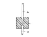
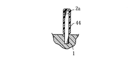
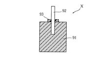
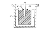
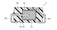
固体電解コンデンサとしては、弁作用を有する金属の多孔質焼結体とこの多孔質焼結体から突出するように設けられた弁作用を有する金属製の陽極ワイヤとを備えるものがある。図15は、このような固体電解コンデンサの製造工程において作成される中間品の一例を示している。この固体電解コンデンサの中間品Xは、弁作用を有する金属の微粉末内に陽極ワイヤ92の一部を挿入した状態で、上記微粉末を加圧成形および焼結することにより、多孔質焼結体91を作成した後に、陽極ワイヤ92のうち多孔質焼結体91寄りの部分に、撥水性の高い樹脂製のリング93を設けることにより作成される。この中間品Xを用いて固体電解コンデンサを製造するには、まず、多孔質焼結体91をリン酸水溶液などの化成液中に、陽極ワイヤ92が設けられた面を上側として浸漬させ、この状態で直流電流を通電させて陽極酸化処理を行うことにより、多孔質焼結体91の内表面、外表面および陽極ワイヤ92の下側の部分に誘電体層(図示略)を形成する。その後に、図16に示すように、多孔質焼結体91を硝酸マンガン水溶液97中に浸漬させ、その後に焼成するといった処理を複数回繰り返すことにより、上記誘電体層上に固体電解質層(図示略)を形成する。図17に示すように、グラファイト層および銀層などからなる導電層94を形成した後に、導通部材95a,95bを接続し、これらを封止樹脂96により封止することにより、固体電解コンデンサYが製造される。
Some solid electrolytic capacitors include a metal porous sintered body having a valve action and a metal anode wire having a valve action provided so as to protrude from the porous sintered body. FIG. 15 shows an example of an intermediate product created in the manufacturing process of such a solid electrolytic capacitor. The intermediate product X of the solid electrolytic capacitor is porous sintered by pressing and sintering the fine powder in a state where a part of the
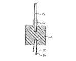
上述した製造方法のうち、上記固体電解質層を形成する工程においては、陽極ワイヤ92のうち上記誘電体層が形成されていない上側の領域に上記固体電解質層を形成してしまうことを防止する必要がある。上記固体電解質層と陽極ワイヤ92とが上記誘電体層を介さずに直接導通すると、固体電解コンデンサYのいわゆるキャパシタとしての機能が適切に発揮されないからである。上述した製造方法においては、図16に良く表れているように、液面97aの位置がリング93の高さの範囲内となるように多孔質焼結体91を保持することにより、陽極ワイヤ92の上部が硝酸マンガン水溶液97に不当に浸ることを回避している。
Of the manufacturing methods described above, in the step of forming the solid electrolyte layer, it is necessary to prevent the solid electrolyte layer from being formed in the upper region of the
しかしながら、図17に良く表れているように、陽極ワイヤ92のうちリング93が設けられた部分は、導通部材95aとの接合には用いることができない。このため、リング93が陽極ワイヤ92の軸方向に長いほど、固体電解コンデンサYが大きくなってしまう。近年、固体電解コンデンサYの小型化の要請が強く、リング93としてもその長さを短くする必要がある。そうすると、図16に示した上記固体電解質層を形成する工程において、液面97aの位置をリング93の高さの範囲内に保つことが困難となり、陽極ワイヤ92の上部が硝酸マンガン水溶液97に不当に浸る虞れが大きくなる。このようなことでは、固体電解コンデンサYにおいて、陽極ワイヤ92が上記固体電解質層と導通することとなり、漏れ電流が過大となったり、いわゆるキャパシタとしての機能が阻害されるなどの不具合を生じていた。
However, as clearly shown in FIG. 17, the portion of the
本発明は、上記した事情のもとで考え出されたものであって、固体電解質層が陽極ワイヤと不当に導通することの防止、および固体電解コンデンサの小型化が可能な固体電解コンデンサの製造方法を提供することをその課題としている。 The present invention has been conceived under the circumstances described above, and it is possible to prevent the solid electrolyte layer from being illegally connected to the anode wire and to manufacture a solid electrolytic capacitor capable of reducing the size of the solid electrolytic capacitor. The challenge is to provide a method.
上記課題を解決するため、本発明では、次の技術的手段を講じている。 In order to solve the above problems, the present invention takes the following technical means.
本発明によって提供される固体電解コンデンサの製造方法は、弁作用を有する金属製の陽極ワイヤが突出するように設けられた弁作用を有する金属の多孔質焼結体の内表面および外表面に、誘電体層を形成する工程と、上記誘電体層上に固体電解質層を形成する工程と、を有する固体電解コンデンサの製造方法であって、上記固体電解質層を形成する工程の前に、上記陽極ワイヤの突出部分の少なくとも一部を被覆部材により覆う工程と、上記固体電解質層を形成する工程の後に、上記被覆部材の少なくとも一部を取り除く工程と、をさらに有することを特徴としている。 The method for producing a solid electrolytic capacitor provided by the present invention includes a metal porous sintered body having a valve action provided so that a metal anode wire having a valve action protrudes on the inner and outer surfaces of the porous sintered body. A method of manufacturing a solid electrolytic capacitor comprising: a step of forming a dielectric layer; and a step of forming a solid electrolyte layer on the dielectric layer, wherein the anode is formed before the step of forming the solid electrolyte layer. The method further comprises a step of covering at least a part of the protruding portion of the wire with a covering member and a step of removing at least a part of the covering member after the step of forming the solid electrolyte layer.
このような構成によれば、上記固体電解質層を形成する工程において、上記被覆部材上に上記固体電解質層が形成されても、上記被覆部材が除去された後は、上記陽極ワイヤのうち上記被覆部材に覆われていた部分は、上記固体電解質層と直接導通することがない。したがって、不当な導通によりいわゆるキャパシタとしての機能が阻害されるなどの不具合を回避して、固体電解コンデンサを適切に製造することができる。たとえば、上記被覆部材により上記陽極ワイヤの大部分を覆う構成とすれば、上記固体電解質層を形成するための処理液の液面に対して、上記固体電解コンデンサを支持すべき高さの範囲が大きくなり、上記固体電解質層の形成を容易に行うことができる。さらに、この製造方法の完成品としての固体電解コンデンサは、上記被覆部材を備えない構成とすることができる。したがって、上記陽極ワイヤの大部分を、たとえばこれと導通する部材との接合に利用することが可能であり、上記固体電解コンデンサの小型化に有利である。 According to such a configuration, in the step of forming the solid electrolyte layer, even if the solid electrolyte layer is formed on the covering member, after the covering member is removed, the covering of the anode wire is the covering member. The portion covered with the member does not directly conduct with the solid electrolyte layer. Accordingly, it is possible to appropriately manufacture a solid electrolytic capacitor while avoiding problems such as impeding the function as a so-called capacitor due to improper conduction. For example, if the coating member is configured to cover most of the anode wire, the range of the height at which the solid electrolytic capacitor should be supported with respect to the liquid level of the treatment liquid for forming the solid electrolyte layer is As a result, the solid electrolyte layer can be easily formed. Furthermore, the solid electrolytic capacitor as a finished product of this manufacturing method can be configured not to include the covering member. Therefore, most of the anode wire can be used, for example, for joining with a member that conducts the anode wire, which is advantageous for downsizing the solid electrolytic capacitor.
本発明の好ましい実施の形態においては、上記陽極ワイヤを覆う工程は、上記誘電体層を形成する工程の前に行う。このような構成によれば、上記誘電体層を形成する工程と上記固体電解質層を形成する工程との間には、上記多孔質焼結体および上記陽極ワイヤなどに加工を施したり、部材を取り付けたりする必要が無い。したがって、上記誘電体層および上記固体電解質層を形成する工程を効率よく行うことができる。 In a preferred embodiment of the present invention, the step of covering the anode wire is performed before the step of forming the dielectric layer. According to such a configuration, between the step of forming the dielectric layer and the step of forming the solid electrolyte layer, the porous sintered body and the anode wire are processed or the member is There is no need to install. Therefore, the process of forming the dielectric layer and the solid electrolyte layer can be performed efficiently.
本発明の好ましい実施の形態においては、上記陽極ワイヤを覆う工程は、上記誘電体層を形成する工程の後に行う。このような構成によれば、上記陽極ワイヤの全体について上記誘電体層の形成を確実化することができる。したがって、上記陽極ワイヤのうち上記誘電体層が形成されていない部分と上記固体電解質層とが不当に導通することを防止するのに好ましい。 In a preferred embodiment of the present invention, the step of covering the anode wire is performed after the step of forming the dielectric layer. According to such a configuration, the formation of the dielectric layer can be ensured for the entire anode wire. Therefore, it is preferable to prevent the portion of the anode wire where the dielectric layer is not formed and the solid electrolyte layer from being unnecessarily conducted.
本発明の好ましい実施の形態においては、上記固体電解質層を形成する工程の後に、上記多孔質焼結体から離間した位置において、上記陽極ワイヤを切断する工程をさらに有する。このような構成によれば、固体電解コンデンサの構成部材として必要な長さよりも長い陽極ワイヤを用意し、その端部付近を挟持すれば、上記誘電体層や固体電解質層を形成する工程を行うのに都合が良い。また、上記陽極ワイヤのうち上記被覆部材により覆われていない端寄りの部分に、上記固体電解質層が直接形成された場合においても、このような部分を切断することにより、固体電解コンデンサにおいて上記陽極ワイヤが上記固体電解質層と不当に導通することを回避することができる。 In a preferred embodiment of the present invention, the method further includes a step of cutting the anode wire at a position separated from the porous sintered body after the step of forming the solid electrolyte layer. According to such a configuration, a process for forming the dielectric layer and the solid electrolyte layer is performed by preparing an anode wire longer than a necessary length as a constituent member of the solid electrolytic capacitor and sandwiching the vicinity of the end thereof. It is convenient for. In addition, even when the solid electrolyte layer is directly formed on a portion of the anode wire that is not covered by the covering member, by cutting such a portion, the anode in the solid electrolytic capacitor It can be avoided that the wire is unreasonably conducted with the solid electrolyte layer.
本発明の好ましい実施の形態においては、上記多孔質焼結体としては、上記陽極ワイヤとして上記多孔質焼結体の互いに異なる面から突出する複数のものが設けられているものを使用し、上記誘電体層および上記固体電解質層を形成する工程においては、上記複数の陽極ワイヤのいずれかの突出部分全体を、上記誘電体層および上記固体電解質層を形成するための処理液のそれぞれに浸漬させる。 In a preferred embodiment of the present invention, as the porous sintered body, one having a plurality of the anode wires protruding from different surfaces of the porous sintered body is used as the anode wire. In the step of forming the dielectric layer and the solid electrolyte layer, the entire protruding portion of any of the plurality of anode wires is immersed in each of the treatment liquids for forming the dielectric layer and the solid electrolyte layer. .
このような構成によれば、上記複数の陽極ワイヤのいずれについても、上記固体電解質層と不当に導通することを回避することができる。上述した従来の製造方法によれば、陽極ワイヤが誘電体層および固体電解質層を形成するための処理液に浸ると、この陽極ワイヤ上に誘電体層と固体電解質層とが形成されることとなる。このため、陽極ワイヤを設けることができるのは、多孔質焼結体の上面に制限されていた。本発明においては、上記複数の陽極ワイヤのうちいずれかの全体が上記処理液に浸されても、その陽極ワイヤに設けられた被覆部材を取り除くことによりこの陽極ワイヤを露出させて、たとえば外部接続用の導通部材と適切に接合することができる。したがって、上記多孔質焼結体の互いに異なる面から突出するように設けられた複数の陽極ワイヤを備える固体電解コンデンサを適切に製造することができる。このような固体電解コンデンサは、上記複数の陽極ワイヤに分散して電流を流すことが可能であり、低抵抗化および低インダクタンス化を図るのに適している。 According to such a configuration, any of the plurality of anode wires can be prevented from being inappropriately connected to the solid electrolyte layer. According to the above-described conventional manufacturing method, when the anode wire is immersed in the treatment liquid for forming the dielectric layer and the solid electrolyte layer, the dielectric layer and the solid electrolyte layer are formed on the anode wire. Become. For this reason, the anode wire can be provided on the upper surface of the porous sintered body. In the present invention, even if any one of the plurality of anode wires is immersed in the processing liquid, the anode wire is exposed by removing the covering member provided on the anode wire, for example, external connection Therefore, it is possible to appropriately join the conductive member. Therefore, it is possible to appropriately manufacture a solid electrolytic capacitor including a plurality of anode wires provided so as to protrude from different surfaces of the porous sintered body. Such a solid electrolytic capacitor can flow a current dispersed in the plurality of anode wires, and is suitable for reducing resistance and inductance.
本発明の好ましい実施の形態においては、上記陽極ワイヤを覆う工程においては、上記被覆部材として、上記陽極ワイヤの軸方向に延びた円筒状のものを使用する。このような構成によれば、上記被覆部材により上記陽極ワイヤの大部分を覆うことが可能であり、上記固体電解質層を形成する工程において、この固体電解質層を形成するための処理液の液面に対して、上記多孔質焼結体を支持すべき高さの範囲を大きくすることができる。また、上記多孔質焼結体のうち上記被覆部材により覆われた部分を小さくすることが可能であり、上記誘電体層および上記固体電解質層を形成するための処理液を上記多孔質焼結体内に適切に浸入させることができる。 In a preferred embodiment of the present invention, in the step of covering the anode wire, a cylindrical member extending in the axial direction of the anode wire is used as the covering member. According to such a configuration, it is possible to cover most of the anode wire with the covering member, and in the step of forming the solid electrolyte layer, the liquid level of the treatment liquid for forming the solid electrolyte layer On the other hand, the range of the height which should support the said porous sintered compact can be enlarged. Further, it is possible to reduce a portion of the porous sintered body covered with the covering member, and a treatment liquid for forming the dielectric layer and the solid electrolyte layer is provided in the porous sintered body. Can be properly infiltrated.
本発明の好ましい実施の形態においては、上記被覆部材を、樹脂により上記陽極ワイヤに接合する。このような構成によれば、上記被覆部材と上記陽極ワイヤとの間の領域に、上記固体電解質層を形成するための処理液が浸入することを防止することができる。また、たとえば後述するリフトオフ技術を用いて上記被覆部材を取り除くのに適した材質の樹脂を用いれば、上記被覆部材を取り除くのに便利である。 In preferable embodiment of this invention, the said coating | coated member is joined to the said anode wire with resin. According to such a structure, it can prevent that the process liquid for forming the said solid electrolyte layer permeates into the area | region between the said covering member and the said anode wire. Further, for example, if a resin made of a material suitable for removing the covering member using a lift-off technique described later is used, it is convenient to remove the covering member.
本発明の好ましい実施の形態においては、上記被覆部材としてガラス管を使用し、このガラス管を上記陽極ワイヤに外嵌させる。このような構成によれば、上記ガラス管は、耐酸性、耐腐食性などに比較的優れるために、上記誘電体層や上記固体電解質層を形成する工程において、腐食されることにより上記陽極ワイヤが不当に露出するといった不具合を回避することができる。 In a preferred embodiment of the present invention, a glass tube is used as the covering member, and the glass tube is externally fitted to the anode wire. According to such a configuration, since the glass tube is relatively excellent in acid resistance, corrosion resistance, and the like, the anode wire is corroded in the step of forming the dielectric layer and the solid electrolyte layer. Can be avoided.
本発明の好ましい実施の形態においては、上記被覆部材として熱収縮性を有する樹脂製の管状部材を使用し、この管状部材を上記陽極ワイヤに外嵌させる。このような構成によれば、上記樹脂製の管状部材を上記陽極ワイヤに設けた後にこれらを加熱することにより、上記管状部材を上記陽極ワイヤに対して十分に接触させることが可能であり、上記管状部材と上記陽極ワイヤとの間の領域に、上記固体電解質層を形成するための処理液が不当に浸入することを防止するのに適している。 In a preferred embodiment of the present invention, a resin tubular member having heat shrinkability is used as the covering member, and the tubular member is externally fitted to the anode wire. According to such a configuration, the tubular member can be sufficiently brought into contact with the anode wire by heating the resin-made tubular member after the resin tubular member is provided on the anode wire. It is suitable for preventing the treatment liquid for forming the solid electrolyte layer from entering the region between the tubular member and the anode wire.
本発明の好ましい実施の形態においては、上記陽極ワイヤを覆う工程においては、金属ワイヤを上記陽極ワイヤに巻き付けることにより上記被覆部材を形成する。このような構成によっても、上記陽極ワイヤが上記固体電解質層と不当に導通することを回避して、固体電解コンデンサを適切に製造することができる。上記金属ワイヤを取り除く工程においては、たとえば上記金属ワイヤの一端部を挟持してこの金属ワイヤを引き剥がすように取り除くことができる。 In a preferred embodiment of the present invention, in the step of covering the anode wire, the covering member is formed by winding a metal wire around the anode wire. Even with such a configuration, it is possible to appropriately manufacture a solid electrolytic capacitor by avoiding that the anode wire is unnecessarily conducted with the solid electrolyte layer. In the step of removing the metal wire, for example, it is possible to remove the metal wire by sandwiching one end of the metal wire and peeling off the metal wire.
本発明の好ましい実施の形態においては、上記陽極ワイヤを覆う工程は、樹脂製の線状部材を上記陽極ワイヤに巻き付けることにより上記被覆部材を形成する。このような構成によっても、上記固体電解コンデンサを適切に製造することができる。 In a preferred embodiment of the present invention, in the step of covering the anode wire, the covering member is formed by winding a resin-made linear member around the anode wire. Even with such a configuration, the solid electrolytic capacitor can be appropriately manufactured.
本発明のその他の特徴および利点は、添付図面を参照して以下に行う詳細な説明によって、より明らかとなろう。 Other features and advantages of the present invention will become more apparent from the detailed description given below with reference to the accompanying drawings.
以下、本発明の好ましい実施の形態につき、図面を参照して具体的に説明する。 Hereinafter, preferred embodiments of the present invention will be specifically described with reference to the drawings.
図1〜図8は、本発明に係る固体電解コンデンサの製造方法の一例を示している。 1 to 8 show an example of a method for manufacturing a solid electrolytic capacitor according to the present invention.
まず、図1に示すように、弁作用を有する金属としてのニオブの多孔質焼結体1を準備する。この多孔質焼結体1には、上向きに突出する陽極ワイヤ2aと、下向きに突出する陽極ワイヤ2bとが設けられている。陽極ワイヤ2aは、陽極ワイヤ2bよりも長い突出寸法とされている。このような多孔質焼結体1は、たとえば、ニオブの微粉末を金型に充填し、この微粉末中に陽極ワイヤ2a,2bのそれぞれの一部ずつを進入させた状態で、加圧成形した後にこれらを焼結することにより作成することができる。
First, as shown in FIG. 1, a porous
多孔質焼結体1を作成した後は、図2に示すように、陽極ワイヤ2a,2bの根元付近に接合樹脂52を塗布する。
After the porous
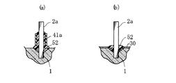
次いで、図3に示すように、陽極ワイヤ2a,2bの外径よりも大きい内径を有する2つのガラス管41a,41bを用意する。これらのガラス管41a,41bの長さは、この製造方法により製造される固体電解コンデンサにおいて外部接続用の導通部材と接合するのに適した程度としておく。これらのガラス管41a,41bを陽極ワイヤ2a,2bそれぞれの根元に向けて嵌め込み、接合樹脂52により陽極ワイヤ2a,2bに接合する。なお、接合樹脂52を塗布する厚さは、上記ガラス管41a,41bと陽極ワイヤ2a,2bとの間の領域を埋めて空隙部を生じさせない厚さとする。
Next, as shown in FIG. 3, two
ガラス管41a,41bを設けた後は、図4に示すように、多孔質焼結体1の内表面および外表面に誘電体層(図示略)を形成する。容器62には、あらかじめ上記誘電体層を形成するための、たとえばリン酸水溶液の化成液61を満たしておく。陽極ワイヤ2aの上端部付近を挟持することにより多孔質焼結体1を支持しつつ、多孔質焼結体1および陽極ワイヤ2a,2bを化成液61中に浸漬させる。この際、陽極ワイヤ2bは、その全体が化成液61中に浸漬され、陽極ワイヤ2aは、ガラス管41a全体が完全に浸る程度に浸漬される。この状態で多孔質焼結体1の内部に化成液61を十分に浸入させた後に、陽極ワイヤ2aと容器62の底面に備えられた電極63との間に、直流電源64により直流電流を通電させる。これにより、多孔質焼結体1の内表面および外表面と、陽極ワイヤ2a,2bとに陽極酸化処理が施され、五酸化ニオブからなる誘電体層が形成される。
After the
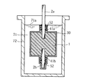
上記誘電体層を形成した後は、図5に示すように、この誘電体層上に固体電解質層30を形成する。容器72には、あらかじめ固体電解質層30を形成するための、たとえば硝酸マンガンの水溶液71を満たしておく。この水溶液71中に、多孔質焼結体1および陽極ワイヤ2a,2bを浸漬させる。本実施形態においては、水溶液71の液面71aがガラス管41aの上端部付近に位置するように、多孔質焼結体1を支持している。なお、多孔質焼結体1の内表面および外表面に固体電解質層30を適切に形成するためには、多孔質焼結体1全体を水溶液71に完全に浸す必要がある。このため、液面71aの位置は、多孔質焼結体1の上面よりも高い位置とすることが望ましく、多孔質焼結体1の上面よりも高い位置であれば、ガラス管41aの上端部付近に限定されず、ガラス管41aの下端部寄りの位置でも良いし、ガラス管41aを超えて陽極ワイヤ2aのうち上記誘電体層が形成されていない上部付近の位置でも良い。多孔質焼結体1の内部に水溶液71を十分に含浸させた後に、多孔質焼結体1を水溶液71から引き揚げて焼成することを複数回にわたって繰り返すことにより、多孔質焼結体1の内表面および外表面、陽極ワイヤ2a,2b、ならびにガラス管41a,41bなどの水溶液71に浸されていた部分に固体電解質層30が形成される。
After the dielectric layer is formed, a
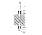
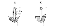
固体電解質層30を形成した後は、図6に示すように、陽極ワイヤ2a,2bを切断する。陽極ワイヤ2a,2bを、多孔質焼結体1から離間した所望の位置において切断することにより、陽極ワイヤ2a,2bの長さを、後述する固体電解コンデンサにおいて、外部接続用の導通部材と接合するのに適した長さとすることができる。なお、本実施形態においては、ガラス管41a,41bの端部付近の位置において陽極ワイヤ2a,2bを切断しているが、切断位置はこれに限定されず、たとえばガラス管41a,41bの中央付近としても良い。
After the
陽極ワイヤ2a,2bを切断した後は、ガラス管41a,41bおよび接合樹脂52を取り除く。これらを取り除く手段としては、たとえば、基板上に配線パターンを形成する際に用いられるいわゆるリフトオフ技術を用いることができる。リフトオフ技術によれば、固体電解質層30のうち、ガラス管41a,41b上に形成された部分のみをガラス管41a,41bおよび接合樹脂52とともに取り除くことができる。このような処理を施すことにより、図7に良く表れているように、多孔質焼結体1の内表面および外表面に固体電解質層30が形成される一方、陽極ワイヤ2a,2b上には固体電解質層30が形成されない。なお、本図中の要部拡大図は、多孔質焼結体1の微視的な構造と、これに誘電体層10および固体電解質層30が積層された構造を示している。本図に良く表れているように、多孔質焼結体1は、多数のニオブの微粒子体11が互いに凝着されて集合されることにより形成されている。これらの多数の微粒子体11間の空隙部に上述した化成液61を浸入させることにより、微粒子体11および陽極ワイヤ2a,2bの表面が陽極酸化処理されることとなり、誘電体層10が形成されている。また、誘電体層10を形成した後の空隙部に水溶液71を浸入させることにより、固体電解質層30が、上記空隙部を埋めるように誘電体層10上に形成されている。この誘電体層10と固体電解質層30との界面が、キャパシタとして機能する部分である。
After the
この後は、図8に示すように、多孔質焼結体1のうち陽極ワイヤ2a,2bが設けられていない側面に形成された固体電解質層30上に、たとえばグラファイト層および銀層を積層させて導電層31を形成する。また、多孔質焼結体1の一側面には、たとえば導電性ペーストを用いて形成された導電層33を介して陰極端子32を接合する。一方、陽極ワイヤ2a,2bそれぞれの突出部分には、導通部材21a,21bおよび陽極端子22a,22bを接合する。これらの多孔質焼結体1、陽極ワイヤ2a,2bなどを封止樹脂51を用いて覆うことにより、固体電解コンデンサAが製造される。この固体電解コンデンサAは、陽極端子22a,22bおよび陰極端子32を備えることにより、いわゆる三端子型の固体電解コンデンサとして構成されている。
Thereafter, as shown in FIG. 8, for example, a graphite layer and a silver layer are laminated on the
本実施形態によれば、陽極ワイヤ2a,2bのうちガラス管41a,41bを取り除くことにより露出された部分は、固体電解質層30と不当に導通することがない。この露出した部分を利用して導通部材21a,21bと十分に導通させることが可能であり、過大な漏れ電流が生じることなどの不具合を回避して固体電解コンデンサAのキャパシタとしての機能を適切に発揮させることができる。
According to the present embodiment, portions of the
また、固体電解質層30を形成する工程においては、液面71aの位置を、陽極ワイヤ2aの軸方向に延びた細長状とされたガラス管41aのいずれかの部分に接する程度の高さとすればよいために、多孔質焼結体1を支持しておくべき高さの範囲を大きくすることができる。したがって、上記工程における作業が容易となる。ガラス管41a,41bが細いほど、多孔質焼結体1のうちガラス管41a,41bにより覆われる領域の大きさを小さくすることが可能であり、化成液61や水溶液71を多孔質焼結体1内に浸入させるのに有利である。
Further, in the step of forming the
さらに、固体電解コンデンサAは、ガラス管41a,41bを備えない構成とすることができる。上述した作業性の向上や陽極ワイヤ2a,2bと固体電解質層30との不当な導通を回避するために、ガラス管41a,41bを細長状としても、固体電解コンデンサAにおいては、これらのガラス管41a,41bのためのスペースが不要である。したがって、固体電解コンデンサAの小型化を図るのに適している。
Furthermore, the solid electrolytic capacitor A can be configured without the
固体電解質層30を形成した後に、陽極ワイヤ2a,2bを所定の長さに切断することにより、これらの陽極ワイヤ2a,2bの長さを、導通部材21a,21bと接続するのに適した所望の長さにすることができる。また、陽極ワイヤ2bについては、固体電解質層30を形成する工程において、その全体が化成液61および水溶液71に浸されるために、ガラス管41bに覆われていない先端部分に固体電解質層30が直接形成される。しかしながら、陽極ワイヤ2bをガラス管41bの先端付近において切断することにより、固体電解質層30が直接形成された先端部分を取り除くことができる。なお、本実施形態とは異なり、液面71aがガラス管41aよりも高い位置となるように多孔質焼結体1が支持されることにより、陽極ワイヤ2aのうちガラス管41aにより覆われていない部分に固体電解質層30が直接形成された場合においても、上述した陽極ワイヤ2bの場合と同様に、陽極ワイヤ2aを切断することにより、固体電解コンデンサAにおいて陽極ワイヤ2aと固体電解質層30とが不当に導通することを回避できる。
After the
ガラス管41a,41bと陽極ワイヤ2a,2bとの間の領域は、接合樹脂52により埋められているために、これらの領域に水溶液71が浸入して固体電解質層30が不当に形成されることを防止することができる。ガラス管41a,41bは、耐酸性および耐腐食性に比較的優れているために、化成液61や水溶液71に含浸させる処理によっても容易には腐食されず、これらの処理を施すのに適している。
Since the regions between the
本実施形態によれば、多孔質焼結体1の互いに異なる面から突出する陽極ワイヤ2a,2bを備える固体電解コンデンサAを適切に製造することができる。本実施形態とは異なり、従来の例のように固体電解質層を形成するための水溶液の液面の高さを安定させるためにリングを利用し、このリングが取り除かれずに固体電解コンデンサに含まれる構成においては、下向きに突出する陽極ワイヤを設けると、この陽極ワイヤは誘電体層と固体電解質層とに覆われてしまう。このようなことでは、この陽極ワイヤに外部接続用の導通部材を適切に接合することができない。また、陽極ワイヤ上に直接形成された固体電解質層のみを取り除く処理を行うことは困難である。本実施形態においては、上述したように、下向きに突出した陽極ワイヤ2bを切断し、ガラス管41bを取り除くことにより、固体電解質層30を適切に取り除くことができる。したがって、陽極ワイヤ2bと導通部材21bとを適切に接合することができる。
According to the present embodiment, the solid electrolytic capacitor A including the
また、固体電解コンデンサAが使用される際には、2つの陽極ワイヤ2a,2bに分散して電流を流すことが可能である。したがって、この固体電解コンデンサAは、低抵抗化および低インダンクタンス化を図るのに好適である。
In addition, when the solid electrolytic capacitor A is used, it is possible to distribute the current to the two
なお、本実施形態とは異なり、誘電体層を形成した後にガラス管41a,41bを接合樹脂52により陽極ワイヤ2a,2bに取り付け、この後に、固体電解質層30を形成する工程としてもよい。このような実施形態によれば、陽極ワイヤ2a,2b上に誘電体層をより確実に形成することができる。したがって、陽極ワイヤ2a,2bのうち誘電体層に覆われていない部分と固体電解質層30とが不当に導通することを防止する点で、好ましい。また、ガラス管41a,41bが設けられる箇所は、陽極ワイヤ2a,2bと多孔質焼結体1との接合部付近である。誘電体層を形成する際に、このような部分が覆われていない状態としておくことは、陽極ワイヤ2a,2bと多孔質焼結体1との接合部に化成液61を浸入させるのに有利である。これらの接合部に誘電体層が適切に形成されると、固体電解質層30と陽極ワイヤ2a,2bとが多孔質焼結体1の内部において不当に導通して漏れ電流が過大となるなどの不具合を回避することができる。
Unlike the present embodiment, after forming the dielectric layer, the
図9〜図14は、本発明の他の実施形態を示している。なお、これらの図において、上記実施形態と同一または類似の要素には、上記実施形態と同一の符号を付している。 9-14 show other embodiments of the present invention. In these drawings, the same or similar elements as those in the above embodiment are denoted by the same reference numerals as those in the above embodiment.
図9に示された実施形態においては、被覆部材として樹脂パイプ42を使用している点が、上記実施形態と異なる。この樹脂パイプ42は、熱収縮性を有する樹脂により形成されている。樹脂パイプ42の内径は、陽極ワイヤ2aの直径よりも大きいものとされている。本図(a)に示すように、この樹脂パイプ42を陽極ワイヤ2aの根元に向けて嵌め込んだ後に、この樹脂パイプ42を所定の温度まで加熱して収縮させることにより、本図(b)に示すように、樹脂パイプ42を陽極ワイヤ2aに密着するように設けることができる。このような実施形態によれば、上述した実施形態における接合樹脂52を塗布する工程を省略することが可能であり、製造工程を簡素化することができる。
The embodiment shown in FIG. 9 is different from the above embodiment in that a
また、ガラス管や樹脂パイプに代えて、図10に示すように、陽極ワイヤ2aに接合樹脂52を塗布した後に、この部分に金属ワイヤ43を螺旋状に巻き付けることにより、本発明でいう被覆部材を形成しても良い。また、金属ワイヤ43に代えて樹脂製の線状部材を巻き付けることによっても、上記被覆部材を形成することができる。このような構成によっても、陽極ワイヤ2a上に固体電解質層が形成されることを防止することができる。なお、金属ワイヤ43は、その一端部を挟持しつつ、巻き付け方向と反対の方向に解くことにより、容易に取り除くことができる。
Further, instead of a glass tube or a resin pipe, as shown in FIG. 10, after applying a
さらに、図11に示すように、陽極ワイヤ2aの全体を覆うように被覆樹脂44を設けても良い。この被覆樹脂44の材料としては、耐酸性、耐腐食性に優れた樹脂を用いることが望ましい。このような実施形態によれば、この陽極ワイヤ2aの全体を固体電解質層を形成するための水溶液71に浸すようにして固体電解質層を形成する場合であっても、被覆樹脂44を取り除くことにより、陽極ワイヤ2aのうち多孔質焼結体1から突出した部分の全体を露出させることができる。このため、陽極ワイヤ2aを切断する工程を省略することができる。
Furthermore, as shown in FIG. 11, a
図12に示された実施形態においては、本図(a)に示すように、接合樹脂52の一部が、陽極ワイヤ2aと多孔質焼結体1との接合部付近に浸入するように設けられている点が、上述した実施形態と異なる。接合樹脂52およびガラス管41aを設けた後に、図4〜図6に示された実施形態と同様にして、誘電体層および固体電解質層を形成する工程を行う。このような実施形態によれば、本図(b)に示すように、陽極ワイヤ2aの根元が接合樹脂52に覆われ、さらにその外側の領域に固体電解質層30が形成される。この接合樹脂52により、陽極ワイヤ2aと固体電解質層30との絶縁が図られるだけでなく、陽極ワイヤ2aと多孔質焼結体1との接合部分の高強度化が可能である。したがって、たとえば陽極ワイヤ2aにモーメントが加えられた場合に、多孔質焼結体1にひび割れが生じることや、この陽極ワイヤ2aが多孔質焼結体1から容易に抜け出すことなどを防止することができる。
In the embodiment shown in FIG. 12, as shown in FIG. 12A, a part of the
図13に示された実施形態においては、本図(a)に示すように、ガラス管41aおよび接合樹脂52と多孔質焼結体1との間に明瞭な隙間が設けられており、この状態において誘電体層および固体電解質層の形成を行う。このような実施形態によれば、本図(b)に示すように、多孔質焼結体1から突出する陽極ワイヤ2aの部分のうち、その根元付近に固体電解質層30を形成することが可能であり、この固体電解質層30によっても、陽極ワイヤ2aと多孔質焼結体1との接合を高強度化することができる。また、図14に示すように、撥水性を有するリング45を多孔質焼結体1から離間させて陽極ワイヤ2aに取り付け、この状態で誘電体層および固体電解質層を形成することによっても、図13(b)に示すような固体電解質層30を適切に形成することができる。なお、固体電解質層30を形成するための処理液が陽極ワイヤ2aの上部に不当に付着することを防止するためには、図1〜図6に示したように、細長の円筒形状を有する被覆部材を用いることが望ましいが、これに限らずリング45のように扁平な形状の被覆部材を用いても良い。
In the embodiment shown in FIG. 13, a clear gap is provided between the
本発明に係る固体電解コンデンサの製造方法は、上述した実施形態に限定されるものではない。 The manufacturing method of the solid electrolytic capacitor according to the present invention is not limited to the above-described embodiment.
リン酸水溶液は、誘電体層を形成するための化成液の一例であり、多孔質焼結体を適切に陽極酸化させることが可能な種々の処理液であればよい。また、固体電解質層を形成するための水溶液としては、硝酸マンガン水溶液に限定されず、たとえば導電性ポリマー液を用いてもよい。 The phosphoric acid aqueous solution is an example of a chemical conversion liquid for forming the dielectric layer, and may be various treatment liquids that can appropriately anodize the porous sintered body. Moreover, the aqueous solution for forming the solid electrolyte layer is not limited to the manganese nitrate aqueous solution, and for example, a conductive polymer solution may be used.
陽極ワイヤの本数は、2本以上であってもよい。また、多孔質焼結体の1つの面から複数の陽極ワイヤが突出するように設けても良い。さらに、陽極ワイヤの突出方向は上下方向に限定されず、たとえば4本の陽極ワイヤが上下左右方向に突出するように設けても良い。 The number of anode wires may be two or more. Moreover, you may provide so that several anode wire may protrude from one surface of a porous sintered compact. Furthermore, the protruding direction of the anode wire is not limited to the vertical direction, and for example, four anode wires may be provided so as to protrude in the vertical and horizontal directions.
被覆部材を取り除く手段としては、上述したリフトオフ技術を用いれば便利であるが、これに限定されず、これ以外のたとえば機械的な切削加工を用いても良い。 As a means for removing the covering member, it is convenient to use the above-described lift-off technique, but the present invention is not limited to this, and other methods such as mechanical cutting may be used.
弁作用を有する金属としては、ニオブに限定されず、それ以外のたとえばタンタルを用いても良い。また、本発明に係る固体電解コンデンサは、その具体的な用途も限定されない。 The metal having a valve action is not limited to niobium, and other materials such as tantalum may be used. Moreover, the specific use of the solid electrolytic capacitor according to the present invention is not limited.
A 固体電解コンデンサ
1 多孔質焼結体
2a,2b 陽極ワイヤ
10 誘電体層
22a,22b 陽極端子
30 固体電解質層
31 導電層
32 陰極端子
41a,41b ガラス管(被覆部材)
42 樹脂パイプ(被覆部材)
43 金属ワイヤ(被覆部材)
44 被覆樹脂(被覆部材)
51 封止樹脂
52 接合樹脂
61 リン酸水溶液(誘電体層を形成するための処理液)
71 硝酸マンガン水溶液(固体電解質層を形成するための処理液)
A Solid
42 Resin pipe (coating material)
43 Metal wire (coating material)
44 Coating resin (coating material)
51
71 Manganese nitrate aqueous solution (treatment liquid for forming solid electrolyte layer)
Claims (11)
上記誘電体層上に固体電解質層を形成する工程と、
を有する固体電解コンデンサの製造方法であって、
上記固体電解質層を形成する工程の前に、上記陽極ワイヤの突出部分の少なくとも一部を被覆部材により覆う工程と、
上記固体電解質層を形成する工程の後に、上記被覆部材の少なくとも一部を取り除く工程と、
をさらに有することを特徴とする、固体電解コンデンサの製造方法。 Forming a dielectric layer on the inner and outer surfaces of a porous sintered metal body having a valve action provided so that a metal anode wire having a valve action protrudes;
Forming a solid electrolyte layer on the dielectric layer;
A method for producing a solid electrolytic capacitor having
Before the step of forming the solid electrolyte layer, a step of covering at least part of the protruding portion of the anode wire with a covering member;
After the step of forming the solid electrolyte layer, removing at least a portion of the covering member;
A method for producing a solid electrolytic capacitor, further comprising:
上記誘電体層および上記固体電解質層を形成する工程においては、上記複数の陽極ワイヤのいずれかの突出部分全体を、上記誘電体層および上記固体電解質層を形成するための処理液のそれぞれに浸漬させる、請求項1ないし4のいずれかに記載の固体電解コンデンサの製造方法。 As the porous sintered body, the anode wire used is provided with a plurality of things protruding from different surfaces of the porous sintered body,
In the step of forming the dielectric layer and the solid electrolyte layer, the entire protruding portion of any of the plurality of anode wires is immersed in each of the treatment liquids for forming the dielectric layer and the solid electrolyte layer. The manufacturing method of the solid electrolytic capacitor in any one of Claim 1 thru | or 4.
Priority Applications (6)
| Application Number | Priority Date | Filing Date | Title |
|---|---|---|---|
| JP2004111101A JP2005294734A (en) | 2004-04-05 | 2004-04-05 | Manufacture for solid electrolytic capacitor |
| US11/547,326 US20070204446A1 (en) | 2004-04-05 | 2005-04-04 | Method for Manufacturing Solid Electrolytic Capacitor |
| PCT/JP2005/006597 WO2005098882A1 (en) | 2004-04-05 | 2005-04-04 | Method for manufacturing solid electrolytic capacitor |
| TW094110728A TWI261848B (en) | 2004-04-05 | 2005-04-04 | Manufacture for solid electrolytic capacitor |
| CNA2005800104902A CN1938800A (en) | 2004-04-05 | 2005-04-04 | Manufacture for solid electrolytic capacitor |
| KR1020067020627A KR20060135865A (en) | 2004-04-05 | 2005-04-04 | Method of manufacturing solid electrolytic capacitor |
Applications Claiming Priority (1)
| Application Number | Priority Date | Filing Date | Title |
|---|---|---|---|
| JP2004111101A JP2005294734A (en) | 2004-04-05 | 2004-04-05 | Manufacture for solid electrolytic capacitor |
Publications (1)
| Publication Number | Publication Date |
|---|---|
| JP2005294734A true JP2005294734A (en) | 2005-10-20 |
Family
ID=35125339
Family Applications (1)
| Application Number | Title | Priority Date | Filing Date |
|---|---|---|---|
| JP2004111101A Pending JP2005294734A (en) | 2004-04-05 | 2004-04-05 | Manufacture for solid electrolytic capacitor |
Country Status (6)
| Country | Link |
|---|---|
| US (1) | US20070204446A1 (en) |
| JP (1) | JP2005294734A (en) |
| KR (1) | KR20060135865A (en) |
| CN (1) | CN1938800A (en) |
| TW (1) | TWI261848B (en) |
| WO (1) | WO2005098882A1 (en) |
Cited By (3)
| Publication number | Priority date | Publication date | Assignee | Title |
|---|---|---|---|---|
| JP2007250920A (en) * | 2006-03-17 | 2007-09-27 | Sanyo Electric Co Ltd | Method for manufacturing solid electrolytic capacitor |
| JP2010062498A (en) * | 2008-09-08 | 2010-03-18 | Nec Tokin Corp | Lower surface electrode type solid electrolytic capacitor and method of manufacturing the same |
| JP2011049339A (en) * | 2009-08-27 | 2011-03-10 | Nec Tokin Corp | Lower-surface electrode type solid electrolytic capacitor and manufacturing method thereof |
Family Cites Families (11)
| Publication number | Priority date | Publication date | Assignee | Title |
|---|---|---|---|---|
| JP2969703B2 (en) * | 1989-12-06 | 1999-11-02 | 松下電器産業株式会社 | Solid electrolytic capacitors |
| US5390074A (en) * | 1991-09-30 | 1995-02-14 | Matsushita Electric Industrial Co., Ltd. | Chip-type solid electrolytic capacitor and method of manufacturing the same |
| JPH0766079A (en) * | 1993-08-25 | 1995-03-10 | Rohm Co Ltd | Manufacture of capacitor element in solid electronic capacitor |
| JPH07153659A (en) * | 1993-11-29 | 1995-06-16 | Sanyo Electric Co Ltd | Reduction-type projection aligner |
| JP3801660B2 (en) * | 1994-05-30 | 2006-07-26 | ローム株式会社 | Method for manufacturing capacitor element for tantalum solid electrolytic capacitor |
| JPH10116753A (en) * | 1997-10-30 | 1998-05-06 | Rohm Co Ltd | Solid electrolytic capacitor |
| US6238444B1 (en) * | 1998-10-07 | 2001-05-29 | Vishay Sprague, Inc. | Method for making tantalum chip capacitor |
| JP2001176753A (en) * | 1999-12-20 | 2001-06-29 | Fujitsu Media Device Kk | Solid electrolytic capacitor |
| JP4547835B2 (en) * | 2001-06-21 | 2010-09-22 | パナソニック株式会社 | Solid electrolytic capacitor and manufacturing method thereof |
| JP4010447B2 (en) * | 2002-05-30 | 2007-11-21 | ローム株式会社 | Solid electrolytic capacitor and manufacturing method thereof |
| US20050237698A1 (en) * | 2004-04-23 | 2005-10-27 | Postage Bradley R | Reduced ESR through use of multiple wire anode |
-
2004
- 2004-04-05 JP JP2004111101A patent/JP2005294734A/en active Pending
-
2005
- 2005-04-04 US US11/547,326 patent/US20070204446A1/en not_active Abandoned
- 2005-04-04 TW TW094110728A patent/TWI261848B/en not_active IP Right Cessation
- 2005-04-04 KR KR1020067020627A patent/KR20060135865A/en not_active Ceased
- 2005-04-04 CN CNA2005800104902A patent/CN1938800A/en active Pending
- 2005-04-04 WO PCT/JP2005/006597 patent/WO2005098882A1/en not_active Ceased
Cited By (3)
| Publication number | Priority date | Publication date | Assignee | Title |
|---|---|---|---|---|
| JP2007250920A (en) * | 2006-03-17 | 2007-09-27 | Sanyo Electric Co Ltd | Method for manufacturing solid electrolytic capacitor |
| JP2010062498A (en) * | 2008-09-08 | 2010-03-18 | Nec Tokin Corp | Lower surface electrode type solid electrolytic capacitor and method of manufacturing the same |
| JP2011049339A (en) * | 2009-08-27 | 2011-03-10 | Nec Tokin Corp | Lower-surface electrode type solid electrolytic capacitor and manufacturing method thereof |
Also Published As
| Publication number | Publication date |
|---|---|
| CN1938800A (en) | 2007-03-28 |
| TWI261848B (en) | 2006-09-11 |
| TW200605115A (en) | 2006-02-01 |
| US20070204446A1 (en) | 2007-09-06 |
| WO2005098882A1 (en) | 2005-10-20 |
| KR20060135865A (en) | 2006-12-29 |
Similar Documents
| Publication | Publication Date | Title |
|---|---|---|
| US8741214B2 (en) | Sintering method, particularly for forming low ESR capacitor anodes | |
| JP2001110688A (en) | Solid electrolytic capacitor and method of manufacturing the same | |
| JP2003163138A (en) | Solid electrolytic capacitor and its manufacturing method | |
| JP2008091784A (en) | Solid electrolytic capacitor, and its manufacturing method | |
| JP2005294734A (en) | Manufacture for solid electrolytic capacitor | |
| JP2019145582A (en) | Solid electrolytic capacitor and method of manufacturing solid electrolytic capacitor | |
| JP5816839B2 (en) | Electrolytic capacitor manufacturing method | |
| JP2005217233A (en) | Solid electrolytic capacitor and its manufacturing method | |
| JPH0493012A (en) | Solid-state electrolytic capacitor and its manufacture | |
| JP2005085779A (en) | Solid electrolytic capacitor | |
| JP2005228801A (en) | Chip-type solid electrolytic capacitor and lead frame used therefor | |
| JP4574544B2 (en) | Solid electrolytic capacitor | |
| JP2003257787A (en) | Solid electrolytic capacitor and its producing method | |
| JP4589187B2 (en) | Manufacturing method of solid electrolytic capacitor | |
| JP4853966B2 (en) | Solid electrolytic capacitor | |
| JP2007227485A (en) | Solid electrolytic capacitor and its manufacturing method | |
| JPH08153650A (en) | Manufacture of solid-state electrolytic capacitor | |
| JP4119167B2 (en) | Manufacturing method of capacitor element used for solid electrolytic capacitor | |
| KR200211021Y1 (en) | Porous Tantalum Pellets of Tantalum Solid Electrolytic Capacitors | |
| JP2006108188A (en) | Solid electrolytic capacitor manufacturing method | |
| JP2004228418A (en) | Capacitor element in solid electrolytic capacitor, and manufacturing method thereof | |
| JP2010153690A (en) | Solid-state electrolytic capacitor and method of manufacturing the same | |
| JP2002222733A (en) | Structure of capacitor element in solid electrolytic capacitor and method of manufacturing the same | |
| JPH03215924A (en) | Manufacture of solid electrolytic capacitor | |
| JP2012033603A (en) | Solid electrolytic capacitor |
Legal Events
| Date | Code | Title | Description |
|---|---|---|---|
| A621 | Written request for application examination |
Free format text: JAPANESE INTERMEDIATE CODE: A621 Effective date: 20070402 |
|
| A131 | Notification of reasons for refusal |
Free format text: JAPANESE INTERMEDIATE CODE: A131 Effective date: 20090901 |
|
| A02 | Decision of refusal |
Free format text: JAPANESE INTERMEDIATE CODE: A02 Effective date: 20100112 |