JP2005294715A - Imaging device and imaging method - Google Patents
Imaging device and imaging method Download PDFInfo
- Publication number
- JP2005294715A JP2005294715A JP2004110740A JP2004110740A JP2005294715A JP 2005294715 A JP2005294715 A JP 2005294715A JP 2004110740 A JP2004110740 A JP 2004110740A JP 2004110740 A JP2004110740 A JP 2004110740A JP 2005294715 A JP2005294715 A JP 2005294715A
- Authority
- JP
- Japan
- Prior art keywords
- inorganic material
- photoelectric conversion
- electrode
- imaging
- imaging device
- Prior art date
- Legal status (The legal status is an assumption and is not a legal conclusion. Google has not performed a legal analysis and makes no representation as to the accuracy of the status listed.)
- Pending
Links
Images


Classifications
-
- H—ELECTRICITY
- H10—SEMICONDUCTOR DEVICES; ELECTRIC SOLID-STATE DEVICES NOT OTHERWISE PROVIDED FOR
- H10K—ORGANIC ELECTRIC SOLID-STATE DEVICES
- H10K39/00—Integrated devices, or assemblies of multiple devices, comprising at least one organic radiation-sensitive element covered by group H10K30/00
- H10K39/30—Devices controlled by radiation
- H10K39/32—Organic image sensors
-
- H—ELECTRICITY
- H01—ELECTRIC ELEMENTS
- H01G—CAPACITORS; CAPACITORS, RECTIFIERS, DETECTORS, SWITCHING DEVICES, LIGHT-SENSITIVE OR TEMPERATURE-SENSITIVE DEVICES OF THE ELECTROLYTIC TYPE
- H01G9/00—Electrolytic capacitors, rectifiers, detectors, switching devices, light-sensitive or temperature-sensitive devices; Processes of their manufacture
- H01G9/20—Light-sensitive devices
- H01G9/2027—Light-sensitive devices comprising an oxide semiconductor electrode
- H01G9/2031—Light-sensitive devices comprising an oxide semiconductor electrode comprising titanium oxide, e.g. TiO2
-
- H—ELECTRICITY
- H10—SEMICONDUCTOR DEVICES; ELECTRIC SOLID-STATE DEVICES NOT OTHERWISE PROVIDED FOR
- H10F—INORGANIC SEMICONDUCTOR DEVICES SENSITIVE TO INFRARED RADIATION, LIGHT, ELECTROMAGNETIC RADIATION OF SHORTER WAVELENGTH OR CORPUSCULAR RADIATION
- H10F39/00—Integrated devices, or assemblies of multiple devices, comprising at least one element covered by group H10F30/00, e.g. radiation detectors comprising photodiode arrays
- H10F39/10—Integrated devices
- H10F39/12—Image sensors
-
- H—ELECTRICITY
- H10—SEMICONDUCTOR DEVICES; ELECTRIC SOLID-STATE DEVICES NOT OTHERWISE PROVIDED FOR
- H10K—ORGANIC ELECTRIC SOLID-STATE DEVICES
- H10K85/00—Organic materials used in the body or electrodes of devices covered by this subclass
- H10K85/30—Coordination compounds
- H10K85/341—Transition metal complexes, e.g. Ru(II)polypyridine complexes
- H10K85/344—Transition metal complexes, e.g. Ru(II)polypyridine complexes comprising ruthenium
-
- Y—GENERAL TAGGING OF NEW TECHNOLOGICAL DEVELOPMENTS; GENERAL TAGGING OF CROSS-SECTIONAL TECHNOLOGIES SPANNING OVER SEVERAL SECTIONS OF THE IPC; TECHNICAL SUBJECTS COVERED BY FORMER USPC CROSS-REFERENCE ART COLLECTIONS [XRACs] AND DIGESTS
- Y02—TECHNOLOGIES OR APPLICATIONS FOR MITIGATION OR ADAPTATION AGAINST CLIMATE CHANGE
- Y02E—REDUCTION OF GREENHOUSE GAS [GHG] EMISSIONS, RELATED TO ENERGY GENERATION, TRANSMISSION OR DISTRIBUTION
- Y02E10/00—Energy generation through renewable energy sources
- Y02E10/50—Photovoltaic [PV] energy
- Y02E10/542—Dye sensitized solar cells
Landscapes
- Engineering & Computer Science (AREA)
- Power Engineering (AREA)
- Microelectronics & Electronic Packaging (AREA)
- Light Receiving Elements (AREA)
- Solid State Image Pick-Up Elements (AREA)
- Transforming Light Signals Into Electric Signals (AREA)
Abstract
【課題】 有機色素を用いた量子効率の高い、かつ耐久性に優れた撮像素子及び撮像方法を提示すること。
【解決手段】 基板上に少なくとも一つの光電変換部位を有する撮像素子において、該光電変換部位が少なくとも一つの電極、少なくとも1種の有機色素、少なくとも一つの無機材料を含み、該有機色素が無機材料に接触して配置されており、かつ、該電極は撮影時に該無機材料に正バイアス電圧を1秒以下印加する電極であることを特徴とする撮像素子及び撮像方法。好ましくは、上記に加えて第2の電極を無機材料に接続して設けた撮像素子及び撮像方法。
【選択図】 なしPROBLEM TO BE SOLVED: To provide an imaging element and an imaging method having high quantum efficiency and excellent durability using an organic dye.
In an imaging device having at least one photoelectric conversion site on a substrate, the photoelectric conversion site includes at least one electrode, at least one organic dye, and at least one inorganic material, and the organic dye is an inorganic material. An image pickup device and an image pickup method, wherein the electrode is an electrode that applies a positive bias voltage to the inorganic material for 1 second or less at the time of photographing. Preferably, in addition to the above, an imaging element and an imaging method provided with the second electrode connected to an inorganic material.
[Selection figure] None
Description
本発明は、撮像素子及びそれを用いる撮像方法に関し、特に量子効率が高い有機色素を用いた撮像素子及びそれを用いる撮像方法に関する。 The present invention relates to an imaging device and an imaging method using the imaging device, and more particularly to an imaging device using an organic dye having high quantum efficiency and an imaging method using the imaging device.
異なる分光感度を有する複数の光電変換素子が積層された受光素子または撮像素子がこれまでに提案されている(特許文献1,特許文献2)。一方、有機色素を用いた光電変換素子は、有機色素の吸収波長制御の自由度から分光特性に優れ、撮像素子の光電変換素子として用いることができ、積層化により光利用効率の向上が見込まれる。しかし、該光電変換素子は、従来の撮像素子に用いられている単結晶Siを用いた光電変換素子に比べて量子効率が低い。例えばよく知られた酸化チタン/金属錯体色素を感光体とするグレッツェル太陽電池は、比較的効率が高い素子であるものの、単結晶Si太陽電池に比べると効率が低いなどの欠点を持つ(非特許文献1及び2参照)。そのため、有機色素を用いた撮像素子の実用化のためにはその改良技術の開発が望まれていた。 A light receiving element or an imaging element in which a plurality of photoelectric conversion elements having different spectral sensitivities are stacked has been proposed (Patent Document 1 and Patent Document 2). On the other hand, photoelectric conversion elements using organic dyes are excellent in spectral characteristics due to the degree of freedom in controlling the absorption wavelength of organic dyes, and can be used as photoelectric conversion elements for imaging elements. . However, the photoelectric conversion element has a lower quantum efficiency than a photoelectric conversion element using single crystal Si used in a conventional imaging element. For example, although a well-known titanium oxide / metal complex dye as a photoreceptor is a Gretzel solar cell, although it is a relatively high-efficiency device, it has disadvantages such as low efficiency compared to a single crystal Si solar cell (non-patent) Reference 1 and 2). Therefore, development of an improved technique has been desired for practical use of an image sensor using an organic dye.
この発明に関連する前記の先行技術には、次ぎの文献がある。
本発明の目的は、有機色素を用いた量子効率が高く、かつ、素子の耐久性(量子効率の経時安定性)が高い撮像素子及び撮像方法を提示することにある。 An object of the present invention is to provide an imaging device and an imaging method using an organic dye and having high quantum efficiency and high device durability (quantity stability over time).
本発明の目的は、以下の手段で達成された。(クレームと同様に修正)
(1)基板上に少なくとも一つの光電変換部位を持つ撮像素子において、該光電変換部位が少なくとも一つの電極、少なくとも一つの有機色素、少なくとも一つの無機材料を含んで該有機色素が無機材料に接触して配置されており、かつ、該電極は該無機材料に撮影時に正のバイアス電圧を1秒以下印加する電極であることを特徴とする撮像素子。
(2)該無機材料の移動度をμ(cm2/V・s)、該無機材料と電極間の距離をd(cm)、該無機材料と該電極間に印加される正バイアス電圧をV(V)とすると、μ×V/d>4×10−4を満たすことを特徴とする(1)に記載の撮像素子。
(3)該無機材料が半導体であることを特徴とする(1)または(2)に記載の撮像素子。
(4)該無機材料が、TiO2、ZnO、SnO2、ITO、ATO、FTO、IZO、SrTiO3、BaTiO2、Ge、Si、III−V族半導体のいずれかを含むことを特徴とする(1)〜(3)のいずれかに記載の撮像素子。
The object of the present invention has been achieved by the following means. (Modified in the same way as the claim)
(1) In an imaging device having at least one photoelectric conversion site on a substrate, the photoelectric conversion site includes at least one electrode, at least one organic dye, and at least one inorganic material, and the organic dye contacts the inorganic material. And an electrode for applying a positive bias voltage to the inorganic material for 1 second or less at the time of photographing.
(2) The mobility of the inorganic material is μ (cm 2 / V · s), the distance between the inorganic material and the electrode is d (cm), and the positive bias voltage applied between the inorganic material and the electrode is V When (V) is satisfied, μ × V / d> 4 × 10 −4 is satisfied. The imaging device according to (1),
(3) The imaging device according to (1) or (2), wherein the inorganic material is a semiconductor.
(4) The inorganic material includes any one of TiO 2 , ZnO, SnO 2 , ITO, ATO, FTO, IZO, SrTiO 3 , BaTiO 2 , Ge, Si, and III-V semiconductors ( The imaging device according to any one of 1) to (3).
(5)該光電変換部位が該無機材料に接続されたもう一つの電極を有し、該電極は該光電変換部位に光が照射されたときに励起された電子を該無機材料から受入れて電子を充電蓄積し、光を遮断すると蓄積した電子を放電する電極であることを特徴とする(1)〜(4)に記載の撮像素子
(6)該光電変換部位が、少なくとも2組積層されていることを特徴とする(1)〜(5)のいずれかに記載の撮像素子。
(7)該光電変換部位が少なくとも3層以上積層されていることを特徴とする(1)〜(6)に記載の撮像素子。
(8)該少なくとも3つの光電変換部位が青色光電変換部位、緑色光電変換部位、赤色光電変換部位からなることを特徴とする(1)〜(7)に記載の撮像素子。
(5) The photoelectric conversion site has another electrode connected to the inorganic material, and the electrode accepts electrons excited when the photoelectric conversion site is irradiated with light from the inorganic material, (6) The imaging device according to any one of (1) to (4), wherein at least two sets of the photoelectric conversion sites are stacked. The imaging device according to any one of (1) to (5), wherein
(7) The imaging device according to any one of (1) to (6), wherein at least three or more photoelectric conversion sites are stacked.
(8) The imaging device according to any one of (1) to (7), wherein the at least three photoelectric conversion sites are a blue photoelectric conversion site, a green photoelectric conversion site, and a red photoelectric conversion site.
(9)上記(1)〜(8)のいずれかに記載の撮像素子を用いて、電極間材料を挟んで又は直接に有機色素と接する電極に対して、無機材料に撮影時に正のバイアス電圧を1秒以下印加することを特徴とする撮像方法。
(10)該正のバイアス電圧が、該無機材料の電荷の移動度をμ(cm2/V・s)、無機材料と電極間の距離をd(cm)、該無機材料と該電極間に印加される正のバイアスをV(V)とするとき、μ×V/d>4×10−4を満たすことを特徴とする上記(9)に記載の撮像方法。
(11)上記(5)に記載の撮像素子の光電変換部位に光を照射して無機材料に接続されたもう一つの電極に電子を励起させ、該励起した電子を無機材料から受け入れて充電蓄積させ、また該照射光を遮断したときに充電蓄積した電子を放電することを特徴とする上記(9)又は(10)に記載の撮像方法。
(9) A positive bias voltage at the time of photographing on an inorganic material with respect to an electrode that is in contact with an organic dye with an interelectrode material interposed therebetween or using the imaging device according to any one of (1) to (8) above Is applied for 1 second or less.
(10) The positive bias voltage is such that the charge mobility of the inorganic material is μ (cm 2 / V · s), the distance between the inorganic material and the electrode is d (cm), and between the inorganic material and the electrode. The imaging method according to (9), wherein μ × V / d> 4 × 10 −4 is satisfied when the applied positive bias is V (V).
(11) The photoelectric conversion site of the imaging device according to (5) is irradiated with light to excite electrons in another electrode connected to the inorganic material, and the excited electrons are received from the inorganic material and charged and accumulated. The imaging method according to (9) or (10), wherein the charged and accumulated electrons are discharged when the irradiation light is interrupted.
上記本発明の特徴は、撮像に際して無機材料に正バイアス電圧を1秒以下印加することであり、この電圧印加によって本発明の目的である量子効率の向上と耐久性の向上(両者の両立)を達成させたことである。
本発明の更なる特徴は、上記バイアス印加に加えて、更にドナー電極とでもいうべきもう一つの電極を無機材料に接続させて設けたことであり、これによって量子効率の更なる向上を達成させたことである。ドナー電極の量子効率向上効果は、発生した励起電子を一旦貯蔵して(すなわち、電子を貯蔵する容量を有する)再結合による無効化を抑止することによってもたらされるものと推定している。なお、この貯蔵された電子(照射された光量に依存する)は電荷転送デバイス等により信号として読み出すことができる。
The feature of the present invention is that a positive bias voltage is applied to the inorganic material for 1 second or less at the time of imaging, and the application of this voltage improves the quantum efficiency and the durability (both compatible), which are the objects of the present invention. It was achieved.
A further feature of the present invention is that, in addition to the bias application, another electrode, which should be called a donor electrode, is provided connected to an inorganic material, thereby further improving quantum efficiency. That is. It is presumed that the quantum efficiency improvement effect of the donor electrode is brought about by temporarily storing the generated excited electrons (that is, having a capacity for storing electrons) and suppressing invalidation due to recombination. The stored electrons (which depend on the amount of light irradiated) can be read out as a signal by a charge transfer device or the like.
有機色素を用い、撮像に際して無機材料に正バイアス電圧を1秒以下印加し、好ましくは更にドナー電極を設けたことを特徴とする本発明の撮像素子及び撮像方法は、量子効率が顕著に高く、しかもその減衰が少なく、したがって高感度で安定した撮像素子を得ることが可能となる。 The image pickup device and the image pickup method of the present invention are characterized in that a positive bias voltage is applied to an inorganic material for 1 second or less at the time of image pickup using an organic dye, and preferably a donor electrode is provided. In addition, it is possible to obtain a highly sensitive and stable image sensor with little attenuation.
以下に本発明の撮像センサ−について説明する。
本発明においては、基板上に少なくとも一つの光電変換部位を持ち、該光電変換部位が少なくとも一つの電極、少なくとも一つの有機色素、少なくとも一つの無機材料を含んで該有機色素が無機材料に接触して配置されており、かつ、該無機材料に該少なくとも一つの電極に対して正バイアスを1秒以下印加することが重要である。本発明における、該無機材料に該少なくとも一つの電極に対して正バイアスを印加するという意味は、例えば該一つの電極がグランドであれば、0より大きい電圧を該無機材料に印加することであり、もちろん、該一つの電極が、負の電位を持てば、それよりも高い電位を該無機材料に与えるということである。
The imaging sensor of the present invention will be described below.
In the present invention, the substrate has at least one photoelectric conversion site, and the photoelectric conversion site contains at least one electrode, at least one organic dye, and at least one inorganic material, and the organic dye contacts the inorganic material. It is important that a positive bias is applied to the inorganic material for at least one second with respect to the at least one electrode. In the present invention, the meaning of applying a positive bias to the inorganic material with respect to the at least one electrode is, for example, that a voltage greater than 0 is applied to the inorganic material if the one electrode is ground. Of course, if the one electrode has a negative potential, a higher potential is applied to the inorganic material.
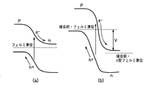
従来のSiを用いたpn接合のフォトダイオードにおいて逆バイアスを印加することによりS/Nを向上させる技術はよく知られているが、本発明におけるバイアス印加とは全く意を異にすることを説明する。従来のSiフォトダイオードにおいては、n型半導体に対してp型半導体側に負のバイアスを印加するという逆バイアスを印加することで空乏層が広がり、また印加した電圧が、光により発生したキャリアーの加速に用いられることで、変換効率が向上するというしくみである。これを図1に示す。図1の(a)は、バイアスがかかっていないSiのpn接合の状態であり、p型とn型のフェルミレベルが合致するまで、キャリアーの拡散が起こり、空乏層が現れる。ここに図1の(b)に示すように逆バイアスをかけると空乏層が広がるため、光により励起された電子が空乏層内でより加速を受け、電荷分離効率が高まる。 A technique for improving the S / N ratio by applying a reverse bias in a conventional pn junction photodiode using Si is well known, but it is completely different from the bias application in the present invention. To do. In a conventional Si photodiode, a depletion layer is expanded by applying a reverse bias of applying a negative bias to the p-type semiconductor side with respect to the n-type semiconductor, and the applied voltage is generated by the carrier generated by light. The conversion efficiency is improved by being used for acceleration. This is shown in FIG. FIG. 1A shows an unbiased Si pn junction state, where carrier diffusion occurs and a depletion layer appears until the p-type and n-type Fermi levels match. When a reverse bias is applied here as shown in FIG. 1 (b), the depletion layer spreads, so that electrons excited by light are further accelerated in the depletion layer, and the charge separation efficiency is increased.
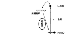
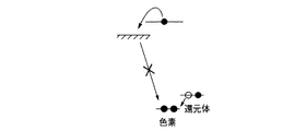
本発明におけるバイアス印加の意味は、上記のメカニズムと違うことを図2で説明し、そのために、印加するバイアスの満たすべき条件が違うことを示す。光により励起された色素のLUMO(励起分子軌道)の電子が無機材料に注入されると、光吸収により発生した色素内の電子と正孔は分離されるが、この電子が正孔と再結合してしまうと光電変換ができない。光により励起された色素の電子が、無機材料に電子を注入する速度は極めて早く、数ps〜数百fsのオーダーである。しかし、この注入された電子が、色素正孔と再結合する速度も数nsオーダーなどとさほど遅くないので、この再結合確率を下げることが重要である。この電子が色素正孔と再結合を防止する一つの良く知られた方法は、この色素正孔を還元する方法である。これを図3によって説明する。図3は、色素が吸着していない側に還元材料であるドナーを配置させておき、色素の電子が光により励起されて電子を注入した後、正孔の存在する準位に再結合速度よりも極めて早い速度で電子を入れる。これにより、再結合する正孔がなくなった電子は、必然的に安定に存在する。この機構により光電変換効率は向上する。しかし、この方式は撮像素子に用いる光電変換部位には適さない。なぜなら、撮像素子の場合は、可逆的な反応が必要であるためである。 The meaning of bias application in the present invention is different from the mechanism described above with reference to FIG. 2, and for this reason, it indicates that the conditions to be applied to the bias to be applied are different. When LUMO (excited molecular orbital) electrons of a dye excited by light are injected into an inorganic material, the electrons and holes in the dye generated by light absorption are separated, but these electrons recombine with holes. If it does, photoelectric conversion cannot be performed. The speed at which the electrons of the dye excited by light inject electrons into the inorganic material is extremely high, on the order of several ps to several hundreds of fs. However, the rate at which the injected electrons recombine with the dye holes is not so slow, such as a few ns order, so it is important to lower the recombination probability. One well-known method for preventing these electrons from recombining with dye holes is to reduce the dye holes. This will be described with reference to FIG. In FIG. 3, a donor which is a reducing material is arranged on the side where the dye is not adsorbed. After the electrons of the dye are excited by light and injected, the recombination velocity is obtained from the level where holes exist. Even put electrons at a very fast rate. As a result, electrons with no recombined holes inevitably exist stably. This mechanism improves the photoelectric conversion efficiency. However, this method is not suitable for a photoelectric conversion site used for an image sensor. This is because an image sensor requires a reversible reaction.
可逆的に光電変換特性を向上させる技術として、本発明では無機材料に正バイアスを該少なくとも一つの電極に対して1秒以下印加することが有効であることがわかった。本発明における1秒以下という条件は、非常に重要である点を説明する。本発明においては有機色素が用いられており、該有機色素に対してバイアスを印加すると、素子の耐久性即ち有機色素の耐久性が悪化する。すなわち、光電変換特性を向上させても有機色素の耐久性が悪化するため、実際には実用化にはほど遠い性能となってしまう。しかし、1秒以下であれば有機色素の耐久性の悪化が極度に抑えられ、かつ、光電変換特性を向上させることができることが、本発明により見出されたのである。より好ましくは100ms以下、さらに好ましくは、10ms以下、さらに好ましくは、1ms以下である。
しかしながら、バイアスを印加しなければ発明の効果が現れないので、少なくとも10ns以上印加するのが好ましい。また、印加時間が1秒を超える場合は有機色素の劣化が著しくなる。
As a technique for reversibly improving the photoelectric conversion characteristics, it has been found effective in the present invention to apply a positive bias to the inorganic material for 1 second or less to the at least one electrode. The point that the condition of 1 second or less in the present invention is very important will be described. In the present invention, an organic dye is used. When a bias is applied to the organic dye, the durability of the element, that is, the durability of the organic dye deteriorates. That is, even if the photoelectric conversion characteristics are improved, the durability of the organic dye is deteriorated, so that the performance is far from practical use. However, it was found by the present invention that the deterioration of the durability of the organic dye can be extremely suppressed and the photoelectric conversion characteristics can be improved if it is 1 second or less. More preferably, it is 100 ms or less, More preferably, it is 10 ms or less, More preferably, it is 1 ms or less.
However, since the effect of the invention does not appear unless a bias is applied, it is preferable to apply at least 10 ns or more. In addition, when the application time exceeds 1 second, the organic dye is significantly deteriorated.
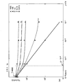
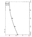
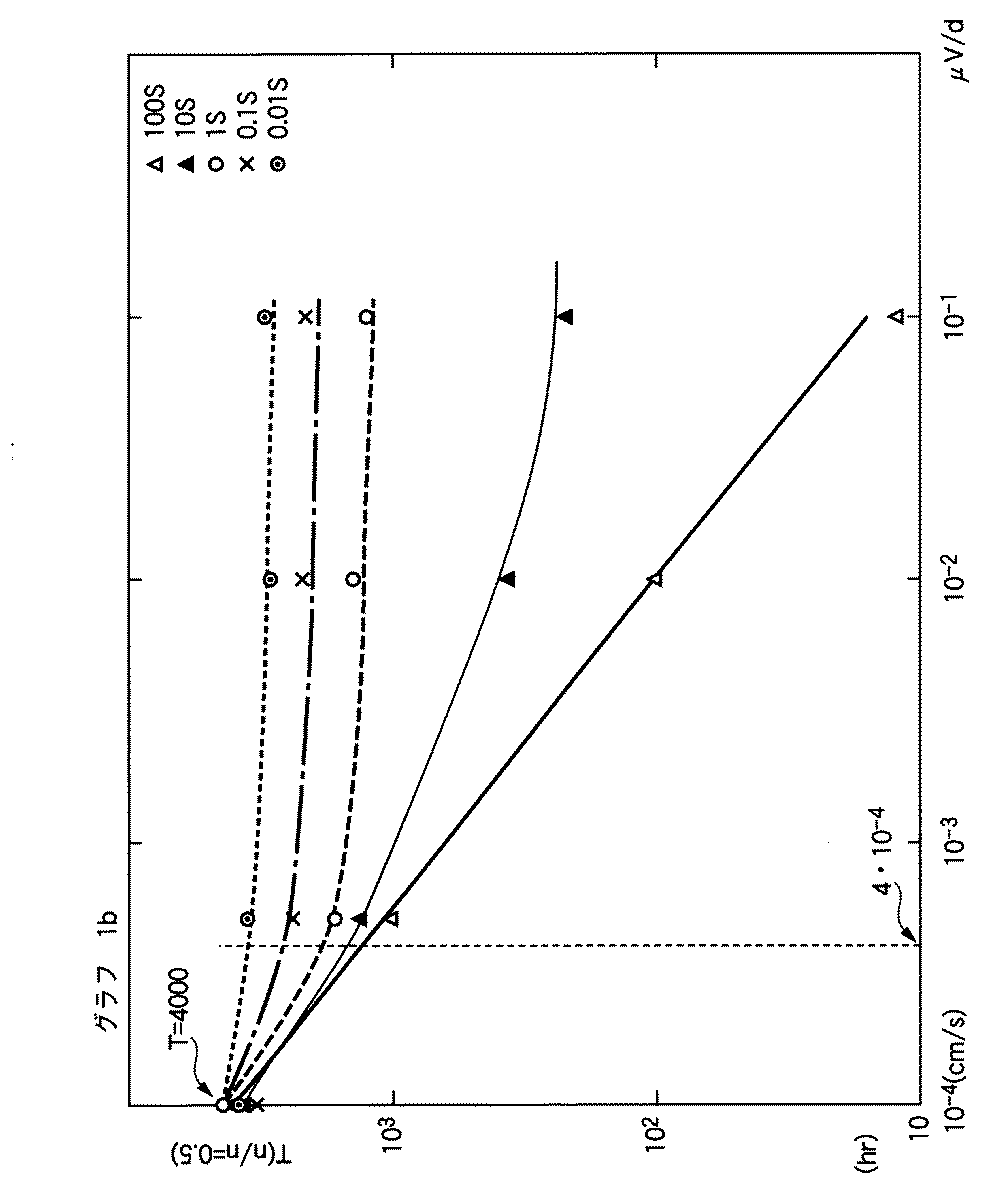
さらに本発明においては、有機色素が吸着している無機材料の移動度をμ(cm2/V・s)、該無機材料と該電極間の距離をd(cm)、該無機材料と該電極間に印加される正バイアス電圧をV(V)とすると、μ×V/d>4×10−4を満たすことが非常に好ましいことが見出された。より好ましくは、μ×V/d>4×10−3であり、より好ましくはμ×V/d>4×10−2であり、μ×V/d>4×10−1である。これを実施例1における図6に示したグラフ1aによって説明する。図6(グラフ1a)の実線は、横軸をμ×V/dとしたときの光電変換素子の量子効率である。μ×V/dを大きくすればするほど、効率が向上することを意味している。このメカニズムは、発明者により以下のように推測されている。図2において、色素が吸着している無機材料の電子が入ることのできる準位に色素のLUMO(励起分子軌道)から電子が注入された状態を考える。ここで、移動度μ、無機材料中に電界Eが存在すると、この電子はμ×Eのドリフト速度を電界から受けるが、このドリフト速度が、色素正孔と無機材料中の再結合速度に対抗できる条件の一つが、μ×V/d>4×10−4となっているのではないかという解釈である。一方、図7に示すグラフ1bは素子の耐久性であり、μ×V/dを大きくすれば、耐久性は大幅に悪化するが、本発明の要件である1秒以下の印加であれば、その耐久性の悪化が大幅に抑えられることがわかる。特に、この効果は、μ×V/d>4×10−4を満たす領域で大幅に改善するため、本発明は、μ×V/d>4×10−4を満たすことが非常に好ましいわけである。 Further, in the present invention, the mobility of the inorganic material adsorbing the organic dye is μ (cm 2 / V · s), the distance between the inorganic material and the electrode is d (cm), the inorganic material and the electrode It has been found that it is very preferable to satisfy μ × V / d> 4 × 10 −4 when the positive bias voltage applied between them is V (V). More preferably, μ × V / d> 4 × 10 −3 , more preferably μ × V / d> 4 × 10 −2 , and μ × V / d> 4 × 10 −1 . This will be described with reference to a graph 1a shown in FIG. The solid line in FIG. 6 (graph 1a) represents the quantum efficiency of the photoelectric conversion element when the horizontal axis is μ × V / d. It means that as the μ × V / d is increased, the efficiency is improved. This mechanism is presumed by the inventors as follows. In FIG. 2, a state is considered in which electrons are injected from the LUMO (excited molecular orbital) of the dye into a level where the electrons of the inorganic material adsorbed by the dye can enter. Here, when the electric field E exists in the inorganic material with mobility μ, the electron receives a μ × E drift velocity from the electric field, and this drift velocity counteracts the recombination velocity in the dye hole and the inorganic material. One of the possible conditions is the interpretation that μ × V / d> 4 × 10 −4 . On the other hand, the graph 1b shown in FIG. 7 shows the durability of the element. If μ × V / d is increased, the durability is greatly deteriorated. However, if the application is 1 second or less, which is a requirement of the present invention, It turns out that the deterioration of the durability can be suppressed significantly. In particular, this effect is, μ × V / d> to significantly improve in areas that meet the 4 × 10 -4, the present invention is, μ × V / d> 4 × 10 -4 is not very preferable to satisfy the It is.
また、本発明において、色素が吸着している無機材料は、色素のLUMO(励起分子軌道)からの電子注入が可能である材料が好ましく、半導体であることが好ましい。本発明に適用される半導体は、一般的な半導体の定義による半導体で室温における電導度が103〜10−10s/cmの範囲の材料である。好ましい半導体の材料としては、シリコン、ゲルマニウムのような単体半導体の他に、金属のカルコゲニドに代表されるような化合物半導体またはペロブスカイト構造を有する化合物等を使用することができる。金属のカルコゲニドとしては好ましくはチタン、スズ、亜鉛、鉄、タングステン、ジルコニウム、ハフニウム、ストロンチウム、インジウム、セリウム、イットリウム、ランタン、バナジウム、ニオブ、あるいはタンタルの酸化物、カドミウム、亜鉛、鉛、銀、アンチモン、ビスマスの硫化物、カドミウム、鉛のセレン化物、カドミウムのテルル化物等が挙げられる。他の化合物半導体としては亜鉛、ガリウム、インジウム、カドミウム、等のリン化物、ガリウム砒素、銅−インジウム−セレン化物、銅−インジウム−硫化物等が挙げられる。また、ペロブスカイト構造を有する化合物としては、チタン酸ストロンチウム、チタン酸カルシウム、チタン酸ナトリウム、チタン酸バリウム、ニオブ酸カリウムなどを挙げることができる。もちろん、これらに限定されるものではない。特に、本発明に好ましい材料としては、TiO2、ZnO、SnO2、ITO(インジウム−錫酸化物)、ATO(アンチモン−酸化錫)、IZO(インジウム−亜鉛酸化物)、FTO(フッ素添加酸化錫)、SrTiO3、BaTiO2、Ge、Si、III−V族系の化合物半導体を挙げることができる。 In the present invention, the inorganic material to which the dye is adsorbed is preferably a material that can inject electrons from the LUMO (excited molecular orbital) of the dye, and is preferably a semiconductor. The semiconductor applied to the present invention is a semiconductor according to a general semiconductor definition and having a conductivity in the range of 10 3 to 10 −10 s / cm at room temperature. As a preferable semiconductor material, a compound semiconductor represented by metal chalcogenide or a compound having a perovskite structure can be used in addition to a single semiconductor such as silicon or germanium. Preferred metal chalcogenides are titanium, tin, zinc, iron, tungsten, zirconium, hafnium, strontium, indium, cerium, yttrium, lanthanum, vanadium, niobium or tantalum oxides, cadmium, zinc, lead, silver, antimony Bismuth sulfide, cadmium, lead selenide, cadmium telluride and the like. Examples of other compound semiconductors include phosphides such as zinc, gallium, indium, and cadmium, gallium arsenide, copper-indium selenide, copper-indium-sulfide, and the like. Examples of the compound having a perovskite structure include strontium titanate, calcium titanate, sodium titanate, barium titanate, and potassium niobate. Of course, it is not limited to these. Particularly preferable materials for the present invention include TiO 2 , ZnO, SnO 2 , ITO (indium-tin oxide), ATO (antimony-tin oxide), IZO (indium-zinc oxide), FTO (fluorine-added tin oxide). ), SrTiO 3 , BaTiO 2 , Ge, Si, and III-V group compound semiconductors.
次に、本発明に用いられる有機色素は、どのようなものでも構わないが、例えば金属錯体色素、シアニン系色素、メロシアニン系色素、フェニルキサンテン系色素、トリフェニルメタン系色素、ロダシアニン系色素、キサンテン系色素、大環状アザアヌレン系色素、アズレン系色素、ナフトキノン、アントラキノン系色素、アントラセン、ピレン等の縮合多環芳香族及び芳香環乃至複素環化合物が縮合した鎖状化合物、スクアリリウム基及びクロコニツクメチン基を結合鎖としてもつ及びキノリン、ベンゾチアゾール、ベンゾオキサゾール等の2ケの含窒素複素環、スクアリリウム基及びクロコニツクメチン基により結合したシアニン系類似の色素等を好ましく用いることができる。金属錯体色素である場合、ジチオール金属錯体系色素、金属フタロシアニン色素、金属ポルフィリン色素又はルテニウム錯体色素が好ましく、ルテニウム錯体色素が特に好ましい。ルテニウム錯体色素としては、例えば米国特許4927721号、同4684537号、同5084365号、同5350644号、同5463057号、同5525440号、特開平7-249790号、特表平10-504512号、WO98/50393号、特開2000-26487号等に記載の錯体色素等が挙げられる。また、シアニン色素、メロシアニン色素、スクワリリウム色素などのポリメチン色素の具体例としては特開平11-35836号、特開平11-67285号、特開平11-86916号、特開平11-97725号、特開平11-158395号、特開平11-163378号、特開平11-214730号、特開平11-214731号、特開平11-238905号、特開2000-26487号、欧州特許892411号、同911841号及び同991092号の各明細書に記載の色素である。 Next, any organic dye may be used in the present invention. For example, metal complex dyes, cyanine dyes, merocyanine dyes, phenylxanthene dyes, triphenylmethane dyes, rhodacyanine dyes, xanthenes. -Type dyes, macrocyclic azaannulene dyes, azulene dyes, naphthoquinones, anthraquinone dyes, chain compounds condensed with condensed polycyclic aromatic and aromatic or heterocyclic compounds such as anthracene, pyrene, squarylium group and croconite methine group And a cyanine-like dye or the like that is bound by two nitrogen-containing heterocycles such as quinoline, benzothiazole, and benzoxazole, a squarylium group, and a croconite methine group can be preferably used. In the case of a metal complex dye, a dithiol metal complex dye, a metal phthalocyanine dye, a metal porphyrin dye or a ruthenium complex dye is preferable, and a ruthenium complex dye is particularly preferable. Examples of the ruthenium complex dye include, for example, U.S. Pat. And complex dyes described in JP-A No. 2000-26487 and the like. Specific examples of polymethine dyes such as cyanine dyes, merocyanine dyes and squarylium dyes are disclosed in JP-A-11-35836, JP-A-11-67285, JP-A-11-86916, JP-A-11-97725, JP-A-11-97725. -158395, JP-A-11-163378, JP-A-11-214730, JP-A-11-214731, JP-A-11-238905, JP-A-2000-26487, European Patents 892411, 918441 and 991092 It is a dye described in each specification of No ..
また、本発明においては有機色素が無機材料に接触して配置されており、どのような配置でも構わないが、有機色素が無機材料に対して吸着していることが好ましい。また該吸着の仕方は物理吸着であっても化学吸着であっても好ましく、どのような吸着でも好ましい。 Moreover, in this invention, the organic pigment | dye is arrange | positioned in contact with an inorganic material, and what arrangement | positioning may be sufficient, but it is preferable that the organic pigment | dye adsorb | sucks with respect to an inorganic material. The adsorption method may be physical adsorption or chemical adsorption, and any adsorption is preferred.
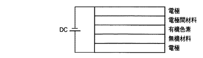
次に、本発明の光電変換部位の好ましい構成に関して述べる。例えば、図4に示すように下方から無機材料、有機色素、電極間材料、少なくとも一つの電極という構成である。また、正バイアスは図4中のDC電源記号のように印加する。また、図5のように無機材料の下に、もう一つの電極(ドナー電極)を配置することも大変望ましい。このようにすると、有機色素から注入される無機材料の特性と、電極特性を分離することができるためである。また、該無機材料は表面積が大きい方が有機色素をたくさん配置しることができるため望ましいことが多く、表面積を大きくする処理がされていることが好ましい。例えば、粒子を焼結することによりポーラスな多孔質膜を作成することも好ましく、薄膜に孔を空けるなどの処理により表面積を増加させる処理をしても良い。無機材料に接して設ける前記ドナー電極は、下記の透明導電膜であることが好ましい。また、該無機材料が透明導電膜であることも非常に好ましく、その場合の該無機材料は電極としての機能も有する。 Next, a preferred configuration of the photoelectric conversion site of the present invention will be described. For example, as shown in FIG. 4, the structure includes an inorganic material, an organic dye, an interelectrode material, and at least one electrode from below. The positive bias is applied as indicated by the DC power supply symbol in FIG. It is also very desirable to arrange another electrode (donor electrode) under the inorganic material as shown in FIG. This is because the characteristics of the inorganic material injected from the organic dye and the electrode characteristics can be separated. In addition, it is often desirable for the inorganic material to have a large surface area because a large amount of organic dye can be arranged, and it is preferable that the surface area be increased. For example, it is also preferable to create a porous porous film by sintering particles, and the surface area may be increased by a process such as making holes in the thin film. The donor electrode provided in contact with the inorganic material is preferably the following transparent conductive film. It is also very preferable that the inorganic material is a transparent conductive film, and the inorganic material in that case also has a function as an electrode.
透明導電膜としては、公知のどのようなものを用いてもよいが、例えば、金属、合金、金属酸化物、有機導電性化合物、これらの混合物等が好適に挙げられ、具体例としては、酸化錫、酸化亜鉛、酸化インジウム、IZO(酸化インジウム亜鉛)、ITO錫(酸化インジウム)等の導電性金属酸化物、金、白金、銀、クロム、ニッケル等の金属、更にこれらの金属と導電性金属酸化物との混合物又は積層物、ヨウ化銅、硫化銅などの無機導電性物質、ポリアニリン、ポリチオフェン、ポリピロ−ル等の有機導電性材料、これらとITOとの積層物、などが挙げられる。また、沢田豊監修「透明導電膜の新展開」(シーエムシー刊、1999年)、日本学術振興会著「透明導電膜の技術」(オーム社、1999年)等に詳細に記載されているものを用いても良い。 Any known conductive film may be used as the transparent conductive film. Examples thereof include metals, alloys, metal oxides, organic conductive compounds, and mixtures thereof. Conductive metal oxides such as tin, zinc oxide, indium oxide, IZO (indium zinc oxide), ITO tin (indium oxide), metals such as gold, platinum, silver, chromium, nickel, and these metals and conductive metals Examples thereof include mixtures or laminates with oxides, inorganic conductive materials such as copper iodide and copper sulfide, organic conductive materials such as polyaniline, polythiophene and polypyrrole, and laminates of these with ITO. Also described in detail by Yutaka Sawada, "New development of transparent conductive film" (published by CMC, 1999), Japan Society for the Promotion of Science "Transparent conductive film technology" (Ohm, 1999), etc. May be used.
本発明における少なくとも一つの電極についても、どのようなものを用いても構わないが、上記透明導電膜が好ましい。もちろん、その他金属、酸化物、半導体何を用いても良く、例えば、Li、Na、Mg、K、Ca、Rb、Sr、Cs、Ba、Fr、Ra、Sc、Ti、Y、Zr、Hf、V、Nb、Ta、Cr、Mo、W、Mn、Tc、Re、Fe,Ru、Os、Co、Rh、Ir、Ni、Pd、Pt、Cu、Ag、Au、Zn、Cd、Al、Ga、In,Tl、Si、Ge、Sn、Pb、P、As、Sb、Bi、Se、Te、Po、Br、I、At、B、C、N、F、O、S、Nの中から選ばれる任意の組み合わせで良い。 Any material may be used as the at least one electrode in the present invention, but the transparent conductive film is preferable. Of course, any other metal, oxide, or semiconductor may be used. For example, Li, Na, Mg, K, Ca, Rb, Sr, Cs, Ba, Fr, Ra, Sc, Ti, Y, Zr, Hf, V, Nb, Ta, Cr, Mo, W, Mn, Tc, Re, Fe, Ru, Os, Co, Rh, Ir, Ni, Pd, Pt, Cu, Ag, Au, Zn, Cd, Al, Ga, In, Tl, Si, Ge, Sn, Pb, P, As, Sb, Bi, Se, Te, Po, Br, I, At, B, C, N, F, O, S, N Any combination is acceptable.
また、上記の電極間材料は、誘電体、導電体、無機半導体、有機半導体、電解質など何であっても構わないが、有機半導体や電解質の中でも溶融塩電解質や固体電解質が好ましい。例えば有機半導体の例では、正孔輸送材料と電子輸送材料があり正孔輸送材料としては、ポリ-N-ビニルカルバゾール誘導体、ポリフェニレンビニレン誘導体、ポリフェニレン、ポリチオフェン、ポリメチルフェニルシラン、ポリアニリン、トリアゾール誘導体、オキサジアゾール誘導体、イミダゾール誘導体、ポリアリールアルカン誘導体、ピラゾリン誘導体及びピラゾロン誘導体、フェニレンジアミン誘導体、アリールアミン誘導体、アミノ置換カルコン誘導体、オキサゾール誘導体、カルバゾール誘導体、スチリルアントラセン誘導体、フルオレノン誘導体、ヒドラゾン誘導体、スチルベン誘導体、ポリフィリン誘導体(フタロシアニン等)、芳香族三級アミン化合物及びスチリルアミン化合物、ブタジエン化合物、ベンジジン誘導体、ポリスチレン誘導体、トリフェニルメタン誘導体、テトラフェニルベンジン誘導体、スターバーストポリアミン誘導体等が使用可能である。また、電子輸送有機材料としては、オキサジアゾール誘導体、トリアゾール誘導体、トリアジン誘導体、ニトロ置換フルオレノン誘導体、チオピランジオキサイド誘導体、ジフェニルキノン誘導体、ペリレンテトラカルボキシル誘導体、アントラキノジメタン誘導体、フレオレニリデンメタン誘導体、アントロン誘導体、ペリノン誘導体、オキシン誘導体、キノリン錯体誘導体等が挙げられる。 The interelectrode material may be a dielectric, a conductor, an inorganic semiconductor, an organic semiconductor, an electrolyte, or the like, but a molten salt electrolyte or a solid electrolyte is preferable among organic semiconductors and electrolytes. For example, in the case of an organic semiconductor, there are a hole transport material and an electron transport material, and as the hole transport material, poly-N-vinylcarbazole derivative, polyphenylene vinylene derivative, polyphenylene, polythiophene, polymethylphenylsilane, polyaniline, triazole derivative, Oxadiazole derivatives, imidazole derivatives, polyarylalkane derivatives, pyrazoline derivatives and pyrazolone derivatives, phenylenediamine derivatives, arylamine derivatives, amino-substituted chalcone derivatives, oxazole derivatives, carbazole derivatives, styrylanthracene derivatives, fluorenone derivatives, hydrazone derivatives, stilbene derivatives , Porphyrin derivatives (phthalocyanine etc.), aromatic tertiary amine compounds and styrylamine compounds, butadiene compounds, benzidine derivatives, Polystyrene derivatives, triphenylmethane derivatives, tetraphenyl benzene derivatives, starburst polyamine derivative or the like can be used. Also, electron transport organic materials include oxadiazole derivatives, triazole derivatives, triazine derivatives, nitro-substituted fluorenone derivatives, thiopyrandioxide derivatives, diphenylquinone derivatives, perylene tetracarboxyl derivatives, anthraquinodimethane derivatives, fluorenylidenemethane. Derivatives, anthrone derivatives, perinone derivatives, oxine derivatives, quinoline complex derivatives, and the like.
溶融塩電解質とは、室温において液状であるか、又は低融点の塩であり、例えばWO95/18456号公報、特開平8―259543号公報及び電気化学,第65巻,11号,923頁(1997年)等に記載されているピリジニウム塩、イミダゾリウム塩、トリアゾリウム塩等の既知の電解質を挙げることができる。100℃以下、特に室温付近において液状となる溶融塩が好ましい。 The molten salt electrolyte is a salt that is liquid at room temperature or has a low melting point. For example, WO95 / 18456, JP-A-8-259543, and Electrochemistry, Vol. 65, No. 11, p. 923 (1997). And other known electrolytes such as pyridinium salts, imidazolium salts, and triazolium salts. A molten salt that is liquid at 100 ° C. or lower, particularly near room temperature, is preferred.
好ましく用いることのできる溶融塩としては、特開2002−299678号公報に記載された一般式(Y-a)、(Y-b)及び(Y-c)により表されるものおよびその例示化合物が挙げられる。 Examples of the molten salt that can be preferably used include those represented by the general formulas (Y-a), (Y-b), and (Y-c) described in JP-A-2002-299678 and exemplified compounds thereof.
上記溶融塩電解質は常温で溶融状態であるものが好ましく、溶媒を用いない方が好ましい。後述する溶媒を添加しても構わないが、溶融塩の含有量は電解質組成物全体に対して50質量%以上であるのが好ましく、90質量%以上であるのが特に好ましい。
また、ゲル電解質としては以下のようなことが挙げられる、ポリマー添加、オイルゲル化剤添加、多官能モノマー類を含む重合、ポリマーの架橋反応等の手法により、前述の溶融塩電解質や電解液をゲル化(固体化)させて使用することもできる。ポリマー添加によりゲル化させる場合は、“Polymer Electrolyte Reviews-1及び2”(J.R.MacCallumとC.A. Vincentの共編、ELSEVIER APPLIED SCIENCE)に記載された化合物を使用することができるが、特にポリアクリロニトリル、ポリフッ化ビニリデンを好ましく使用することができる。オイルゲル化剤添加によりゲル化させる場合はJ. Chem Soc. Japan, Ind. Chem.Sec., 46巻,779頁(1943), J. Am. Chem. Soc., 111巻,5542頁(1989), J. Chem. Soc., Chem. Commun., 1993、390頁, Angew. Chem. Int. Ed. Engl., 35巻,1949頁(1996), Chem. Lett., 1996, 885頁, J. Chm. Soc.,Chem. Commun., 1997,545頁に記載されている化合物を使用することができるが、好ましい化合物は分子構造中にアミド構造を有する化合物である。電解液をゲル化した例は特開平11-185863号公報に、溶融塩電解質をゲル化した例は特開2000-58140号公報に記載されており、本発明にも適用できる。
The molten salt electrolyte is preferably in a molten state at room temperature, and preferably does not use a solvent. Although the solvent described later may be added, the content of the molten salt is preferably 50% by mass or more, and particularly preferably 90% by mass or more with respect to the entire electrolyte composition.
In addition, the gel electrolyte can be prepared by adding polymer, oil gelling agent, polymerization containing polyfunctional monomers, polymer cross-linking reaction, etc. It can also be used after being solidified. When gelation is performed by adding a polymer, compounds described in “Polymer Electrolyte Reviews-1 and 2” (JRMacCallum and CA Vincent, ELSEVIER APPLIED SCIENCE) can be used. Can be preferably used. In the case of gelation by adding an oil gelling agent, J. Chem Soc. Japan, Ind. Chem. Sec., 46, 779 (1943), J. Am. Chem. Soc., 111, 5542 (1989) , J. Chem. Soc., Chem. Commun., 1993, 390, Angew. Chem. Int. Ed. Engl., 35, 1949 (1996), Chem. Lett., 1996, p. 885, J. Although compounds described in Chm. Soc., Chem. Commun., 1997, page 545 can be used, preferred compounds are compounds having an amide structure in the molecular structure. An example of gelling the electrolytic solution is described in JP-A No. 11-185863, and an example of gelling the molten salt electrolyte is described in JP-A No. 2000-58140, which can also be applied to the present invention.
また、ポリマーの架橋反応により電解質をゲル化させる場合、架橋可能な反応性基を含有するポリマー及び架橋剤を併用することが望ましい。この場合、好ましい架橋可能な反応性基は、アミノ基、含窒素複素環(例えば、ピリジン環、イミダゾール環、チアゾール環、オキサゾール環、トリアゾール環、モルホリン環、ピペリジン環、ピペラジン環など)であり、好ましい架橋剤は、窒素原子に対して求電子反応可能な2官能以上の試薬(例えば、ハロゲン化アルキル、ハロゲン化アラルキル、スルホン酸エステル、酸無水物、酸クロライド、イソシアネート、α、β-不飽和スルホニル基、α、β-不飽和カルボニル基、α、β-不飽和ニトリル基など)であり、特開2000-17076号公報、同2000-86724号公報に記載されている架橋技術も適用できる。
次に、高分子化合物としては、高分子化合物自体が電解質塩を溶解してイオン伝導性を示すもの、或いは、高分子化合物自体は電解質塩を溶解できないものであっても電解質塩を溶解することができる溶媒を用いて、高分子化合物がイオン伝導性を示すようになるものを用いることができる。
When the electrolyte is gelled by a polymer crosslinking reaction, it is desirable to use a polymer containing a crosslinkable reactive group and a crosslinking agent in combination. In this case, preferred crosslinkable reactive groups are amino groups and nitrogen-containing heterocycles (for example, pyridine ring, imidazole ring, thiazole ring, oxazole ring, triazole ring, morpholine ring, piperidine ring, piperazine ring, etc.) Preferred cross-linking agents are bifunctional or higher reagents capable of electrophilic reaction with a nitrogen atom (for example, alkyl halide, halogenated aralkyl, sulfonate ester, acid anhydride, acid chloride, isocyanate, α, β-unsaturated). A sulfonyl group, an α, β-unsaturated carbonyl group, an α, β-unsaturated nitrile group, etc.), and the crosslinking techniques described in JP-A Nos. 2000-17076 and 2000-86724 can also be applied.
Next, as the polymer compound, the polymer compound itself dissolves the electrolyte salt and exhibits ionic conductivity, or the polymer compound itself dissolves the electrolyte salt even if it cannot dissolve the electrolyte salt. A solvent that can exhibit high ionic conductivity can be used using a solvent that can be used.
前者の高分子化合物としては、例えば、ポリエチレングリコール、主鎖にポリアクリル酸、ポリメタクリル酸、ポリエチレンオキシド、ポリプロピレンオキシド、ポリビニルアルコール、ポリフォスファゼン、ポリシラン等、また、それらの共重合体等の構造を有し、側鎖にポリオキシエチレン構造を有する高分子化合物等を用いることができる。これらの電解質塩を溶解できる高分子化合物であっても、前述の電解質塩を溶解することができる溶媒を併用することができる。 Examples of the former polymer compound include, for example, polyethylene glycol, polyacrylic acid, polymethacrylic acid, polyethylene oxide, polypropylene oxide, polyvinyl alcohol, polyphosphazene, polysilane, etc. in the main chain, and their copolymers. And a polymer compound having a polyoxyethylene structure in the side chain can be used. Even if it is a high molecular compound which can melt | dissolve these electrolyte salts, the solvent which can melt | dissolve the above-mentioned electrolyte salt can be used together.
これに対して、後者の高分子化合物としては、例えば、ポリ塩化ビニル、ポリアクリロニトリル、ポリエチレン、ポリプロピレン、ポリエステル、ポリアクリレートまた、それらの共重合体等を用いることができる。なお、上述の高分子化合物は、架橋構造を有するものであっても良い。
また、本発明においては上記光電変換部位が、少なくとも2層以上積層されていることも好ましく、より好ましくは3層以上である。なぜなら、そうすることにより光利用効率を高めることができるからである。加えて、少なくとも3つの光電変換部位が青色光電変換部位、緑色光電変換部位、赤色光電変換部位であれば、1ピクセルでフルカラー撮像素子として機能することができ、大変好ましい。
また、本発明に用いる基板は、電荷転送デバイスを載せたSiウェハー、CMOSイメージセンサーの駆動回路を載せたSiウェハーなどのSi基板が最も好ましく、その他半導体基板、ガラス基板、プラスチック基板など何を用いても良い。
On the other hand, as the latter polymer compound, for example, polyvinyl chloride, polyacrylonitrile, polyethylene, polypropylene, polyester, polyacrylate, or a copolymer thereof can be used. Note that the above-described polymer compound may have a crosslinked structure.
In the present invention, it is also preferable that at least two or more photoelectric conversion sites are laminated, more preferably three or more layers. This is because the light utilization efficiency can be increased by doing so. In addition, if at least three photoelectric conversion sites are a blue photoelectric conversion site, a green photoelectric conversion site, and a red photoelectric conversion site, one pixel can function as a full-color imaging device, which is very preferable.
The substrate used in the present invention is most preferably a Si substrate such as a Si wafer on which a charge transfer device is mounted, a Si wafer on which a CMOS image sensor driving circuit is mounted, and any other substrate such as a semiconductor substrate, a glass substrate, or a plastic substrate is used. May be.
以下、本発明を実施例によって具体的に説明するが、本発明はこれらに限定されるものではない。
フッ素をドープした酸化スズをコーティングした導電性ガラス(旭硝子製TCOガラス-Uを20mm×20mmの大きさに切断加工したもの)の導電面側にガラス棒を用いて、ソーラロニクス(社)製酸化チタンゾル液(酸化チタン粒径9nm)を塗布した。塗布後、室温で1日間風乾した。次に、このガラスを電気炉(ヤマト科学製マッフル炉FP-32型)に入れ、450℃にて30分間焼成した。このガラスを炉から取り出し冷却した後、ルテニウムトリスビピリジン錯体色素のエタノール溶液(3×10⁻⁴mol/L)に3時間浸漬した。色素を吸着したガラスを4-t-ブチルピリジンに15分間浸漬した後、エタノールで洗浄し自然乾燥させた。このようにして得られる感光層の厚さは10μmであり、半導体微粒子の塗布量は20g/m2とした。なお、導電性ガラスの表面抵抗は約30Ω/□であった。このようにして作成した色素増感されたTiO2半導体電極基板(2cm×2cm)に、同じ大きさの白金蒸着ガラスを、さまざまな厚み(0.1μm、1μm、10μm、25μm)のスペーサーを用いて重ね合わせた後、両ガラスの隙間に毛細管現象を利用して電解質(LiN(SO2CF3)2(0.5M)/メトキシアセトニトリル)を染み込ませ、素子を作成した。
EXAMPLES Hereinafter, the present invention will be specifically described with reference to examples, but the present invention is not limited to these examples.
Oxidation manufactured by Solaronics Co., Ltd. using a glass rod on the conductive surface of conductive glass coated with tin oxide doped with fluorine (Asahi Glass TCO glass-U cut to a size of 20mm x 20mm) A titanium sol solution (titanium oxide particle size 9 nm) was applied. After coating, it was air-dried at room temperature for 1 day. Next, this glass was put in an electric furnace (Yamato Scientific muffle furnace FP-32 type) and baked at 450 ° C. for 30 minutes. The glass was taken out of the furnace and cooled, and then immersed in an ethanol solution of ruthenium trisbipyridine complex dye (3 × 10 −4 mol / L) for 3 hours. The glass adsorbed with the dye was immersed in 4-t-butylpyridine for 15 minutes, then washed with ethanol and air dried. The thickness of the photosensitive layer thus obtained was 10 μm, and the coating amount of semiconductor fine particles was 20 g / m 2 . The surface resistance of the conductive glass was about 30Ω / □. The dye-sensitized TiO 2 semiconductor electrode substrate (2 cm × 2 cm) prepared in this way is coated with the same size of platinum-deposited glass using spacers of various thicknesses (0.1 μm, 1 μm, 10 μm, 25 μm). Then, an electrolyte (LiN (SO 2 CF 3 ) 2 (0.5M) / methoxyacetonitrile) was infiltrated into the gap between the two glasses using a capillary phenomenon to produce a device.
上述のようにして作成した受光素子に、1mW〜50μWの白色光を1/100秒間照射し、流れる電流を測定した。そのときの流れる電流と光源の光子数から外部量子効率を計算し、図6のグラフ1aに示した。また、色素が吸着した酸化チタン電極付き透明電極に、白金電極に電極に対して、正となるような電圧をt秒(100s、10s、1s、0.1s、0.01s)印加し、その際に流れる電流と光源の光子数から外部量子効率(h)を計算した。なお、電圧を印加しても光を照射していない場合、流れる電流は0であった。また、この試験を10秒に1回行い、量子効率が半分になってしまう時間(T(n/n=0.5))を求め、この結果を図7にグラフ化して示した。 The light receiving element produced as described above was irradiated with 1 mW to 50 μW of white light for 1/100 second, and the flowing current was measured. The external quantum efficiency was calculated from the current flowing at that time and the number of photons of the light source, and is shown in graph 1a of FIG. In addition, a voltage that is positive with respect to the platinum electrode is applied to the transparent electrode with the titanium oxide electrode on which the dye is adsorbed with respect to the electrode for t seconds (100 s, 10 s, 1 s, 0.1 s, 0.01 s). The external quantum efficiency (h) was calculated from the current flowing and the number of photons of the light source. When no voltage was applied even when a voltage was applied, the flowing current was zero. Further, this test was performed once every 10 seconds, the time (T (n / n = 0.5)) during which the quantum efficiency was halved was determined, and the results are shown in a graph in FIG.
これらのグラフから明らかなように、1秒以下の印加においては、μV/dを大きくすると量子効率が上昇するにも関わらず、耐久性の劣化が大幅に軽減することがわかる。また、特にμV/d>4×10−4の領域においては、1s以下の印加時間では耐久性の悪化がほとんどなく、量子効率を向上させることができるため非常に好ましいことがわかる。 As can be seen from these graphs, in the application for 1 second or less, when μV / d is increased, although the quantum efficiency is increased, the deterioration of durability is significantly reduced. In particular, in the region of μV / d> 4 × 10 −4 , it can be seen that the application time of 1 s or less hardly deteriorates the durability and can improve the quantum efficiency, which is very preferable.
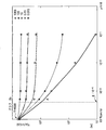
コーニング1737ガラス(25mm×25mm)上に反応性スパッタ製膜を用いて表面抵抗7Ω/□、厚み0.20μmのITOを製膜した。このITOを5mmの幅、5mm間隔の2本のライン上にパターニングを行った。この上から、化合物1を厚み10nmで真空製膜を行った。この後、Alq(トリス−8−ヒドロキシキノリンアルミニウム)を厚み80nmで真空製膜し、最後にAlを0.5μmで真空蒸着した。なお、最後のAlはマスクを介してITOのラインと交差するように同様の2本のラインを作成した。ここに実施例1と同様に外部量子効率を計算し、図8にグラフ化して示した。なお、光を照射しなくても電流が流れてしまう場合、光を照射したときに流れる電流と差をとることで計算を行った。また、この試験を10秒に1回行い、量子効率が半分になってしまう時間を求め、この結果を図9にグラフ化して示した。 An ITO film having a surface resistance of 7Ω / □ and a thickness of 0.20 μm was formed on a Corning 1737 glass (25 mm × 25 mm) using a reactive sputtering film. This ITO was patterned on two lines having a width of 5 mm and an interval of 5 mm. From this, the compound 1 was vacuum-deposited with a thickness of 10 nm. Thereafter, Alq (tris-8-hydroxyquinoline aluminum) was vacuum-deposited with a thickness of 80 nm, and finally Al was vacuum-deposited with a thickness of 0.5 μm. Two similar lines were created so that the last Al crossed the ITO line through a mask. Here, the external quantum efficiency was calculated in the same manner as in Example 1, and is shown in a graph in FIG. In addition, when the current flows without irradiating light, the calculation was performed by taking a difference from the current flowing when the light was irradiated. In addition, this test was performed once every 10 seconds, the time for which the quantum efficiency was halved was determined, and the result is shown in a graph in FIG.
これらのグラフから実施例1と全く同様の効果が読み取れる。即ち、1秒以下の印加においては、μV/dを大きくすると量子効率が上昇するにも関わらず、耐久性の劣化が大幅に軽減すること、特にμV/d>4×10−4の領域においては、1s以下の印加時間では耐久性の悪化がほとんどないことが示されていて、このことから量子効率を向上させることができることが判る。 From these graphs, the same effect as in Example 1 can be read. In other words, in the application of 1 second or less, although the quantum efficiency increases when μV / d is increased, the deterioration of durability is greatly reduced, particularly in the region of μV / d> 4 × 10 −4 . Shows that there is almost no deterioration in durability at an application time of 1 s or less. From this, it can be seen that the quantum efficiency can be improved.
Claims (11)
Priority Applications (3)
| Application Number | Priority Date | Filing Date | Title |
|---|---|---|---|
| JP2004110740A JP2005294715A (en) | 2004-04-05 | 2004-04-05 | Imaging device and imaging method |
| US11/098,401 US20050224819A1 (en) | 2004-04-05 | 2005-04-05 | Imaging device and imaging method |
| US11/826,113 US20070262231A1 (en) | 2004-04-05 | 2007-07-12 | Imaging device and imaging method |
Applications Claiming Priority (1)
| Application Number | Priority Date | Filing Date | Title |
|---|---|---|---|
| JP2004110740A JP2005294715A (en) | 2004-04-05 | 2004-04-05 | Imaging device and imaging method |
Publications (1)
| Publication Number | Publication Date |
|---|---|
| JP2005294715A true JP2005294715A (en) | 2005-10-20 |
Family
ID=35059681
Family Applications (1)
| Application Number | Title | Priority Date | Filing Date |
|---|---|---|---|
| JP2004110740A Pending JP2005294715A (en) | 2004-04-05 | 2004-04-05 | Imaging device and imaging method |
Country Status (2)
| Country | Link |
|---|---|
| US (2) | US20050224819A1 (en) |
| JP (1) | JP2005294715A (en) |
Families Citing this family (6)
| Publication number | Priority date | Publication date | Assignee | Title |
|---|---|---|---|---|
| JP5609119B2 (en) * | 2009-01-21 | 2014-10-22 | ソニー株式会社 | Solid-state imaging device, manufacturing method thereof, and imaging device |
| TWI416716B (en) * | 2009-01-21 | 2013-11-21 | Sony Corp | Solid-state imaging device, manufacturing method thereof, and imaging device |
| US8665363B2 (en) * | 2009-01-21 | 2014-03-04 | Sony Corporation | Solid-state image device, method for producing the same, and image pickup apparatus |
| CN102005304B (en) * | 2010-12-01 | 2013-02-27 | 北京科技大学 | Preparation method for SiO2-ZnO nano-bar array composite electrode |
| JP2017059655A (en) * | 2015-09-16 | 2017-03-23 | ソニー株式会社 | Solid-state imaging device and method of manufacturing solid-state imaging device |
| JP6796814B2 (en) * | 2016-06-21 | 2020-12-09 | パナソニックIpマネジメント株式会社 | Solar cell system and how to operate the solar cell system |
Family Cites Families (6)
| Publication number | Priority date | Publication date | Assignee | Title |
|---|---|---|---|---|
| US6391528B1 (en) * | 2000-04-03 | 2002-05-21 | 3M Innovative Properties Company | Methods of making wire grid optical elements by preferential deposition of material on a substrate |
| US7220914B2 (en) * | 2003-12-01 | 2007-05-22 | Konarka Technologies, Inc. | Zwitterionic compounds and photovoltaic cells containing same |
| WO2001096454A1 (en) * | 2000-06-12 | 2001-12-20 | Maxdem Incorporated | Polymer matrix electroluminescent materials and devices |
| SG113443A1 (en) * | 2001-12-05 | 2005-08-29 | Semiconductor Energy Laboratao | Organic semiconductor element |
| JP2003257671A (en) * | 2002-02-28 | 2003-09-12 | Fuji Photo Film Co Ltd | Light emitting device and manufacturing method thereof |
| US7129466B2 (en) * | 2002-05-08 | 2006-10-31 | Canon Kabushiki Kaisha | Color image pickup device and color light-receiving device |
-
2004
- 2004-04-05 JP JP2004110740A patent/JP2005294715A/en active Pending
-
2005
- 2005-04-05 US US11/098,401 patent/US20050224819A1/en not_active Abandoned
-
2007
- 2007-07-12 US US11/826,113 patent/US20070262231A1/en not_active Abandoned
Also Published As
| Publication number | Publication date |
|---|---|
| US20070262231A1 (en) | 2007-11-15 |
| US20050224819A1 (en) | 2005-10-13 |
Similar Documents
| Publication | Publication Date | Title |
|---|---|---|
| JP6337561B2 (en) | Perovskite solar cell | |
| US9614169B2 (en) | Back contact perovskite solar cell | |
| EP1075005B1 (en) | Electrolyte composition, and photo-electro-chemical cell | |
| JP4610160B2 (en) | Photoelectric conversion material, semiconductor electrode, and photoelectric conversion element using the same | |
| US7309833B2 (en) | Photovoltaic devices comprising layer(s) of photoactive organics dissolved in high Tg polymers | |
| US20070262231A1 (en) | Imaging device and imaging method | |
| JP2011065751A (en) | Photoelectric conversion element | |
| WO2016038825A1 (en) | Back contact perovskite solar cell | |
| CN100533777C (en) | Multilayer structure, photoelectric conversion element, and electronic device | |
| Kashif et al. | Polypyridyl iron complex as a hole-transporting material for formamidinium lead bromide perovskite solar cells | |
| JP4111360B2 (en) | Gel electrolyte, gel electrolyte for photoelectrochemical cell, and photoelectrochemical cell | |
| JP2005132914A (en) | Photoelectric conversion material, semiconductor electrode, and photoelectric conversion element using the same | |
| EP1020881A2 (en) | Photo-electrochemical cell | |
| JP2004235011A (en) | Electrolyte solution using iodine-cyclodextrin clathrate and photoelectric conversion element using the same | |
| US10483045B2 (en) | Solar cell | |
| JP2005311329A (en) | Photoelectric conversion element and imaging element | |
| JP4326272B2 (en) | Dye-sensitized solar cell dye | |
| JPH0434833B2 (en) | ||
| JP2005340489A (en) | Photoelectric conversion element, imaging device and photoelectric conversion method | |
| JP4285673B2 (en) | Photoelectric conversion type color light sensor and image sensor | |
| JP2006190534A (en) | Photoelectric conversion material, semiconductor electrode, and photoelectric conversion element using the same | |
| JP2000100485A (en) | Electrolyte and photoelectrochemical battery | |
| JP2005063833A (en) | Photoelectric conversion material, semiconductor electrode, and photoelectric conversion element using the same | |
| JP2000058891A (en) | Electrolyte, electrolyte for photoelectric chemical cell, photoelectric chemical battery and pyridinium compound | |
| JP5185517B2 (en) | Photoelectric conversion material, semiconductor electrode, and photoelectric conversion element using the same |
Legal Events
| Date | Code | Title | Description |
|---|---|---|---|
| RD04 | Notification of resignation of power of attorney |
Free format text: JAPANESE INTERMEDIATE CODE: A7424 Effective date: 20060327 |
|
| A711 | Notification of change in applicant |
Free format text: JAPANESE INTERMEDIATE CODE: A712 Effective date: 20061124 |