JP2005294548A - Network electronic component and manufacturing method thereof - Google Patents

Network electronic component and manufacturing method thereof Download PDF

Info

Publication number
JP2005294548A
JP2005294548A JP2004107800A JP2004107800A JP2005294548A JP 2005294548 A JP2005294548 A JP 2005294548A JP 2004107800 A JP2004107800 A JP 2004107800A JP 2004107800 A JP2004107800 A JP 2004107800A JP 2005294548 A JP2005294548 A JP 2005294548A
Authority
JP
Japan
Prior art keywords
thin film
electronic component
network electronic
passive element
film passive
Prior art date
Legal status (The legal status is an assumption and is not a legal conclusion. Google has not performed a legal analysis and makes no representation as to the accuracy of the status listed.)
Pending
Application number
JP2004107800A
Other languages
Japanese (ja)
Inventor
Shinji Wakizaka
伸治 脇坂
Current Assignee (The listed assignees may be inaccurate. Google has not performed a legal analysis and makes no representation or warranty as to the accuracy of the list.)
Casio Computer Co Ltd
Original Assignee
Casio Computer Co Ltd
Priority date (The priority date is an assumption and is not a legal conclusion. Google has not performed a legal analysis and makes no representation as to the accuracy of the date listed.)
Filing date
Publication date
Application filed by Casio Computer Co Ltd filed Critical Casio Computer Co Ltd
Priority to JP2004107800A priority Critical patent/JP2005294548A/en
Priority to US11/093,571 priority patent/US7808073B2/en
Publication of JP2005294548A publication Critical patent/JP2005294548A/en
Pending legal-status Critical Current

Links

Images

Classifications

    • HELECTRICITY
    • H01ELECTRIC ELEMENTS
    • H01LSEMICONDUCTOR DEVICES NOT COVERED BY CLASS H10
    • H01L2224/00Indexing scheme for arrangements for connecting or disconnecting semiconductor or solid-state bodies and methods related thereto as covered by H01L24/00
    • H01L2224/01Means for bonding being attached to, or being formed on, the surface to be connected, e.g. chip-to-package, die-attach, "first-level" interconnects; Manufacturing methods related thereto
    • H01L2224/10Bump connectors; Manufacturing methods related thereto
    • H01L2224/11Manufacturing methods
    • HELECTRICITY
    • H01ELECTRIC ELEMENTS
    • H01LSEMICONDUCTOR DEVICES NOT COVERED BY CLASS H10
    • H01L2924/00Indexing scheme for arrangements or methods for connecting or disconnecting semiconductor or solid-state bodies as covered by H01L24/00
    • H01L2924/013Alloys
    • H01L2924/014Solder alloys

Landscapes

  • Semiconductor Integrated Circuits (AREA)

Abstract

<P>PROBLEM TO BE SOLVED: To provide a network electronic component having a simple structure capable of simplifying the manufacturing process thereof by providing externally connecting electrodes only on a substrate. <P>SOLUTION: Thin film resistors 3, connecting pads 4, wiring 10 including underlying metal layers 9, pillar-shaped electrodes 11, and solder balls 13 are collectively formed in a region where a plurality of network electronic components are formed on the silicon substrate 1 in a wafer state, and then the plurality of network electronic components are obtained by dividing along dicing streets 23. <P>COPYRIGHT: (C)2006,JPO&NCIPI

Description

この発明はネットワーク電子部品およびその製造方法に関する。   The present invention relates to a network electronic component and a manufacturing method thereof.

従来のネットワーク電子部品には、相互に分離された複数の薄膜抵抗素子を備えたものがある(例えば、特許文献1参照)。このネットワーク電子部品では、セラミックス基板の両側面に複数の溝が設けられ、セラミックス基板の上面において溝に対応しない部分に複数対の上部電極が設けられ、セラミックス基板の下面において溝に対応しない部分に複数対の下部電極が設けられ、セラミックス基板の両側面において溝に対応しない部分に複数対の側面電極がそれぞれ対応する上部電極および下部電極に接続されて設けられ、各対の上部電極間に薄膜抵抗体が設けられ、薄膜抵抗体等を含むセラミックス基板上に保護ガラス層、中間ガラス層および被覆ガラス層が設けられ、この状態で露出された上部電極、下部電極および側面電極からなる電極部の表面にニッケルメッキおよび半田メッキが設けられた構造となっている。   Some conventional network electronic components include a plurality of thin film resistor elements separated from each other (see, for example, Patent Document 1). In this network electronic component, a plurality of grooves are provided on both side surfaces of the ceramic substrate, a plurality of pairs of upper electrodes are provided on a portion of the upper surface of the ceramic substrate that does not correspond to the groove, and a portion of the lower surface of the ceramic substrate that does not correspond to the groove. A plurality of pairs of lower electrodes are provided, and a plurality of pairs of side electrodes are connected to the corresponding upper and lower electrodes at portions not corresponding to the grooves on both sides of the ceramic substrate, and a thin film is provided between the upper electrodes of each pair. A resistor is provided, and a protective glass layer, an intermediate glass layer, and a covering glass layer are provided on a ceramic substrate including a thin film resistor, etc., and an electrode portion including an upper electrode, a lower electrode, and a side electrode exposed in this state is provided. It has a structure in which nickel plating and solder plating are provided on the surface.

特開2000−348914号公報JP 2000-348914 A

ところで、上記構造のネットワーク電子部品を製造する場合には、完成されたネットワーク電子部品を複数個形成することが可能な面積を有する集合セラミックス基板の上面に第1ブレーク溝および第2ブレーク溝を格子状に形成し、第1ブレーク溝上における集合セラミックス基板に側面溝形成用のスルーホールを形成し、集合セラミックス基板の上面に電極ペーストを印刷して上部電極を形成し、集合セラミックス基板の下面に電極ペーストを印刷して下部電極を形成し、対の上部電極間に抵抗体ペーストを印刷して薄膜抵抗体を形成し、薄膜抵抗体を保護するための保護ガラス層を印刷して形成し、中間ガラス層および被覆ガラス層を印刷して形成し、集合セラミックス基板を第1ブレーク溝に沿って切断して両側面に溝を有する複数のバー状セラミックス基板に分割し、バー状セラミックス基板の両側面に電極ペーストを塗布して側面電極を形成し、バー状セラミックス基板を第2ブレーク溝に沿って切断して複数の単体セラミックス基板に分割し、単体セラミックス基板の上部電極、下部電極および側面電極からなる電極部の表面にニッケルメッキおよび半田メッキを形成している。   By the way, when the network electronic component having the above structure is manufactured, the first break groove and the second break groove are formed on the upper surface of the aggregate ceramic substrate having an area where a plurality of completed network electronic components can be formed. The through-hole for forming the side surface groove is formed in the aggregate ceramic substrate on the first break groove, the electrode paste is printed on the upper surface of the aggregate ceramic substrate to form the upper electrode, and the electrode is formed on the lower surface of the aggregate ceramic substrate. The paste is printed to form the lower electrode, the resistor paste is printed between the pair of upper electrodes, the thin film resistor is formed, and the protective glass layer for protecting the thin film resistor is printed and formed. A plurality of glass layers and coated glass layers formed by printing and having a groove on both sides by cutting the aggregate ceramic substrate along the first break groove Divide into bar-shaped ceramic substrates, apply electrode paste on both sides of the bar-shaped ceramic substrate to form side electrodes, cut the bar-shaped ceramic substrate along the second break groove, and divide into multiple single ceramic substrates In addition, nickel plating and solder plating are formed on the surface of the electrode portion including the upper electrode, the lower electrode, and the side electrode of the single ceramic substrate.

しかしながら、上記構造のネットワーク電子部品では、電極部を、セラミックス基板の上面において溝に対応しない部分に設けられた上部電極と、セラミックス基板の下面において溝に対応しない部分に設けられた下部電極と、セラミックス基板の両側面において溝に対応しない部分に設けられた側面電極とによって構成しているので、構造が複雑である上、製造工程が極めて繁雑であるという問題があった。製造工程について説明すると、第1ブレーク溝および第2ブレーク溝形成工程、スルーホール形成工程、上部電極形成工程、下部電極形成工程、薄膜抵抗体形成工程、保護ガラス層形成工程、中間ガラス層および被覆ガラス層形成工程、第1ブレーク溝切断工程、側面電極形成工程、第2ブレーク溝切断工程、ニッケルメッキおよび半田メッキ形成工程、というように工程数が多く、しかも、側面電極形成工程は第1ブレーク溝切断工程後であり、ニッケルメッキおよび半田メッキ形成工程は第2ブレーク溝切断工程後であり、製造工程が極めて繁雑となってしまう。   However, in the network electronic component having the above structure, the electrode portion includes an upper electrode provided in a portion not corresponding to the groove on the upper surface of the ceramic substrate, and a lower electrode provided in a portion not corresponding to the groove on the lower surface of the ceramic substrate, Since both sides of the ceramic substrate are constituted by side electrodes provided in portions not corresponding to the grooves, there is a problem that the structure is complicated and the manufacturing process is extremely complicated. The manufacturing process will be described. First break groove and second break groove forming process, through-hole forming process, upper electrode forming process, lower electrode forming process, thin film resistor forming process, protective glass layer forming process, intermediate glass layer and coating There are many steps such as a glass layer forming step, a first break groove cutting step, a side electrode forming step, a second break groove cutting step, a nickel plating and a solder plating forming step, and the side electrode forming step is the first break step. After the groove cutting step, the nickel plating and solder plating forming steps are after the second break groove cutting step, and the manufacturing process becomes extremely complicated.

そこで、この発明は、構造が簡単で、製造工程を簡略化することができるネットワーク電子部品を提供することを目的とする。   Therefore, an object of the present invention is to provide a network electronic component that has a simple structure and can simplify the manufacturing process.

この発明は、上記目的を達成するため、基板と、前記基板上に設けられた薄膜受動素子と、前記薄膜受動素子を含む前記基板上に前記薄膜受動素子に接続されて設けられた複数の外部接続用電極とを有することを特徴とするものである。   To achieve the above object, the present invention provides a substrate, a thin film passive device provided on the substrate, and a plurality of external devices connected to the thin film passive device on the substrate including the thin film passive device. And a connection electrode.

この発明によれば、基板上にのみ外部接続用電極を設けているので、構造が簡単で、製造工程を簡略化することができる。   According to the present invention, since the external connection electrode is provided only on the substrate, the structure is simple and the manufacturing process can be simplified.

(第1実施形態)
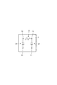
図1はこの発明の第1実施形態としてのネットワーク電子部品の等価回路的平面図を示す。このネットワーク電子部品では、平面正方形状のシリコン基板(半導体基板)1上に2つの薄膜抵抗素子(薄膜受動素子)2が相互に分離されて設けられている。この場合、薄膜抵抗素子2の両端部は、後述する柱状電極11からなる外部接続用電極に接続されている。
(First embodiment)
FIG. 1 is an equivalent circuit plan view of a network electronic component as a first embodiment of the present invention. In this network electronic component, two thin film resistance elements (thin film passive elements) 2 are provided separately on a silicon substrate (semiconductor substrate) 1 having a planar square shape. In this case, both ends of the thin film resistance element 2 are connected to an external connection electrode composed of a columnar electrode 11 described later.

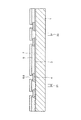
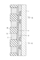
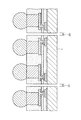
次に、図2は図1に示すネットワーク電子部品の平面図を示し、図3は図2のIII−III線に沿う断面図を示す。図3を参照して説明すると、シリコン基板1の上面にはNiCrやTaN等からなる短冊形状の薄膜抵抗体3が設けられている。薄膜抵抗体3の両端部上面にはアルミニウム系金属等からなる複数の接続パッド4が設けられている。接続パッド4の中央部を除く領域において薄膜抵抗体3を含むシリコン基板1の上面には酸化シリコン等からなる絶縁膜5が設けられ、接続パッド4の中央部は絶縁膜5に設けられた開口部6を介して露出されている。   2 is a plan view of the network electronic component shown in FIG. 1, and FIG. 3 is a cross-sectional view taken along line III-III in FIG. Referring to FIG. 3, a strip-shaped thin film resistor 3 made of NiCr, TaN or the like is provided on the upper surface of the silicon substrate 1. A plurality of connection pads 4 made of aluminum metal or the like are provided on the upper surfaces of both end portions of the thin film resistor 3. An insulating film 5 made of silicon oxide or the like is provided on the upper surface of the silicon substrate 1 including the thin film resistor 3 in a region excluding the central portion of the connection pad 4, and the central portion of the connection pad 4 is an opening provided in the insulating film 5. It is exposed through the part 6.

絶縁膜5の上面にはポリイミド系樹脂やエポキシ系樹脂等からなる保護膜(絶縁膜)7が設けられている。この場合、絶縁膜5の開口部6に対応する部分における保護膜7には開口部8が設けられている。保護膜7の上面には銅等からなる下地金属層9が設けられている。下地金属層9の上面全体には銅からなる配線10が設けられている。下地金属層9を含む配線10の一端部は、両開口部6、8を介して接続パッド4に接続されている。   A protective film (insulating film) 7 made of polyimide resin, epoxy resin, or the like is provided on the upper surface of the insulating film 5. In this case, an opening 8 is provided in the protective film 7 in a portion corresponding to the opening 6 of the insulating film 5. A base metal layer 9 made of copper or the like is provided on the upper surface of the protective film 7. A wiring 10 made of copper is provided on the entire upper surface of the base metal layer 9. One end of the wiring 10 including the base metal layer 9 is connected to the connection pad 4 through both openings 6 and 8.

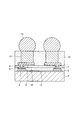
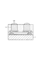
配線10の接続パッド部上面には銅からなる柱状電極11が設けられている。配線10を含む保護膜7の上面にはエポキシ系樹脂やポリイミド系樹脂等からなる封止膜12がその上面が柱状電極11の上面と面一となるように設けられている。柱状電極11の上面には半田ボール13が設けられている。   A columnar electrode 11 made of copper is provided on the upper surface of the connection pad portion of the wiring 10. A sealing film 12 made of an epoxy resin, a polyimide resin, or the like is provided on the upper surface of the protective film 7 including the wiring 10 so that the upper surface is flush with the upper surface of the columnar electrode 11. A solder ball 13 is provided on the upper surface of the columnar electrode 11.

ところで、図1に示すように、平面正方形状のシリコン基板1上には2つの薄膜抵抗素子2が相互に分離されて設けられ、4つの柱状電極11からなる外部接続用電極が2行2列に配置されている。したがって、図2に示すように、柱状電極11および半田ボール13は2行2列に配置されている。ここで、このネットワーク電子部品の一部の寸法の一例について説明すると、シリコン基板1のサイズは1.0mm×1.0mmであり、柱状電極11のピッチは0.5mmであり、柱状電極11の直径は0.25mmである。   By the way, as shown in FIG. 1, two thin film resistance elements 2 are provided on a planar square silicon substrate 1 so as to be separated from each other, and external connection electrodes including four columnar electrodes 11 are arranged in two rows and two columns. Is arranged. Therefore, as shown in FIG. 2, the columnar electrodes 11 and the solder balls 13 are arranged in 2 rows and 2 columns. Here, an example of a part of the dimensions of the network electronic component will be described. The size of the silicon substrate 1 is 1.0 mm × 1.0 mm, the pitch of the columnar electrodes 11 is 0.5 mm, The diameter is 0.25 mm.

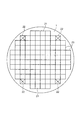
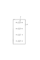
次に、このネットワーク電子部品の製造方法の一例について説明する。まず、図4に示すように、ウエハ状態のシリコン基板(半導体基板)1を用意する。ここで、図4において、縦線と横線とで囲まれた正方形状で無印の領域はネットワーク電子部品形成領域21であり、×印の領域はアライメントマーク形成領域22である。したがって、縦線および横線はダイシングストリート23である。ただし、ダイシングストリート23は、シリコン基板1の上面に実際に形成されているものではなく、設計上の仮想線である。   Next, an example of a method for manufacturing the network electronic component will be described. First, as shown in FIG. 4, a silicon substrate (semiconductor substrate) 1 in a wafer state is prepared. Here, in FIG. 4, a square and unmarked region surrounded by vertical and horizontal lines is a network electronic component forming region 21, and an × mark region is an alignment mark forming region 22. Therefore, the vertical line and the horizontal line are dicing streets 23. However, the dicing street 23 is not actually formed on the upper surface of the silicon substrate 1 but is a virtual line in design.

次に、図5に示すように、ウエハ状態のシリコン基板1の上面にNiCrやTaN等からなる短冊形状の薄膜抵抗体3を印刷、焼成により形成する。この状態では、図4に示す1つの正方形状のネットワーク電子部品形成領域21におけるシリコン基板1の上面に2つの短冊形状の薄膜抵抗体3が互いに平行に形成されている。次に、薄膜抵抗体3の両端部上面にアルミニウム系金属等からなる接続パッド4を形成する。   Next, as shown in FIG. 5, a strip-shaped thin film resistor 3 made of NiCr, TaN or the like is formed on the upper surface of the silicon substrate 1 in a wafer state by printing and baking. In this state, two strip-shaped thin film resistors 3 are formed in parallel to each other on the upper surface of the silicon substrate 1 in one square network electronic component forming region 21 shown in FIG. Next, connection pads 4 made of aluminum metal or the like are formed on the upper surfaces of both end portions of the thin film resistor 3.

次に、薄膜抵抗体3および接続パッド4を含むシリコン基板1の上面全体に酸化シリコン等からなる絶縁膜5を形成する。次に、接続パッド4の中央部に対応する部分における絶縁膜5に開口部6を形成する。次に、開口部5内を含む前記煙幕5の上面全体にポリイミド系樹脂やエポキシ系樹脂等からなる保護膜7を形成する。次に、絶縁膜5の開口部6に対応する部分における保護膜7に開口部8を形成する。   Next, an insulating film 5 made of silicon oxide or the like is formed on the entire upper surface of the silicon substrate 1 including the thin film resistor 3 and the connection pad 4. Next, an opening 6 is formed in the insulating film 5 in a portion corresponding to the central portion of the connection pad 4. Next, a protective film 7 made of polyimide resin or epoxy resin is formed on the entire upper surface of the smoke screen 5 including the inside of the opening 5. Next, an opening 8 is formed in the protective film 7 in a portion corresponding to the opening 6 of the insulating film 5.

次に、図6に示すように、両開口部6、8を介して露出された接続パッド4の上面を含む保護膜7の上面全体に下地金属層9を形成する。この場合、下地金属層9は、無電解メッキにより形成された銅層のみであってもよく、またスパッタにより形成された銅層のみであってもよく、さらにスパッタにより形成されたチタン等の薄膜層上にスパッタにより銅層を形成したものであってもよい。   Next, as shown in FIG. 6, a base metal layer 9 is formed on the entire upper surface of the protective film 7 including the upper surface of the connection pad 4 exposed through both openings 6 and 8. In this case, the base metal layer 9 may be only a copper layer formed by electroless plating, may be only a copper layer formed by sputtering, or a thin film such as titanium formed by sputtering. A copper layer may be formed on the layer by sputtering.

次に、下地金属層9の上面にメッキレジスト膜24をパターン形成する。この場合、配線10形成領域に対応する部分におけるメッキレジスト膜24には開口部25が形成されている。次に、下地金属層9をメッキ電流路として銅の電解メッキを行なうことにより、メッキレジスト膜24の開口部25内の下地金属層9の上面に配線10を形成する。次に、メッキレジスト膜24を剥離する。   Next, a plating resist film 24 is patterned on the upper surface of the base metal layer 9. In this case, an opening 25 is formed in the plating resist film 24 in a portion corresponding to the wiring 10 formation region. Next, by performing copper electroplating using the base metal layer 9 as a plating current path, the wiring 10 is formed on the upper surface of the base metal layer 9 in the opening 25 of the plating resist film 24. Next, the plating resist film 24 is peeled off.

次に、図7に示すように、配線10を含む下地金属層9の上面にメッキレジスト膜26をパターン形成する。この場合、柱状電極11形成領域に対応する部分におけるメッキレジスト膜26には開口部27が形成されている。次に、下地金属層9をメッキ電流路として銅の電解メッキを行なうことにより、メッキレジスト膜26の開口部27内の配線10の接続パッド部上面に柱状電極11を形成する。次に、メッキレジスト膜26を剥離し、次いで、配線10をマスクとして下地金属層9の不要な部分をエッチングして除去すると、図8に示すように、配線10下にのみ下地金属層9が残存される。   Next, as shown in FIG. 7, a plating resist film 26 is patterned on the upper surface of the base metal layer 9 including the wiring 10. In this case, an opening 27 is formed in the plating resist film 26 in a portion corresponding to the columnar electrode 11 formation region. Next, the columnar electrode 11 is formed on the upper surface of the connection pad portion of the wiring 10 in the opening 27 of the plating resist film 26 by performing electrolytic plating of copper using the base metal layer 9 as a plating current path. Next, the plating resist film 26 is peeled off, and then unnecessary portions of the base metal layer 9 are removed by etching using the wiring 10 as a mask, so that the base metal layer 9 is formed only under the wiring 10 as shown in FIG. Remain.

次に、図9に示すように、スクリーン印刷法、スピンコーティング法、ダイコート法等により、柱状電極11および配線10を含む保護膜7の上面全体にエポキシ系樹脂やポリイミド系樹脂等からなる封止膜12をその厚さが柱状電極11の高さよりも厚くなるように形成する。したがって、この状態では、柱状電極11の上面は封止膜12によって覆われている。   Next, as shown in FIG. 9, the entire upper surface of the protective film 7 including the columnar electrode 11 and the wiring 10 is sealed with an epoxy resin, a polyimide resin, or the like by screen printing, spin coating, die coating, or the like. The film 12 is formed so that its thickness is greater than the height of the columnar electrode 11. Therefore, in this state, the upper surface of the columnar electrode 11 is covered with the sealing film 12.

次に、封止膜12および柱状電極11の上面側を適宜に研磨し、図10に示すように、柱状電極11の上面を露出させ、且つ、この露出された柱状電極11の上面を含む封止膜12の上面を平坦化する。ここで、柱状電極11の上面側を適宜に研磨するのは、電解メッキにより形成される柱状電極11の高さにばらつきがあるため、このばらつきを解消して、柱状電極11の高さを均一にするためである。   Next, the upper surface side of the sealing film 12 and the columnar electrode 11 is appropriately polished to expose the upper surface of the columnar electrode 11 and to include the exposed upper surface of the columnar electrode 11 as shown in FIG. The upper surface of the stop film 12 is flattened. Here, the reason why the upper surface side of the columnar electrode 11 is appropriately polished is that there is a variation in the height of the columnar electrode 11 formed by electrolytic plating, so that this variation is eliminated and the height of the columnar electrode 11 is made uniform. It is to make it.

次に、図11に示すように、柱状電極11の上面に半田ボール13を形成する。次に、シリコン基板1の下面をダイシングテープ(図示せず)に貼り付け、図4に示すアライメントマーク形成領域22に形成されたアライメントマーク(図示せず)を基準として、図12に示すように、シリコン基板1等をダイシングストリート23に沿って切断し、ダイシングテープから剥がすと、図2に示すネットワーク電子部品が複数個得られる。   Next, as shown in FIG. 11, solder balls 13 are formed on the upper surface of the columnar electrode 11. Next, the lower surface of the silicon substrate 1 is attached to a dicing tape (not shown), and the alignment mark (not shown) formed in the alignment mark formation region 22 shown in FIG. When the silicon substrate 1 or the like is cut along the dicing street 23 and peeled off from the dicing tape, a plurality of network electronic components shown in FIG. 2 are obtained.

このようにして得られたネットワーク電子部品では、シリコン基板1上にのみ外部接続用電極としての柱状電極11を設けているので、構造が簡単である。また、上記製造方法では、ウエハ状態のシリコン基板1上の複数のネットワーク電子部品形成領域21に対して、薄膜抵抗体3、接続パッド4、配線10、柱状電極11および半田ボール13の形成を一括して行い、その後にダイシングストリート23に沿って分断して複数個のネットワーク電子部品を得ているので、製造工程を簡略化することができる。   The network electronic component obtained in this way has a simple structure because the columnar electrode 11 as an external connection electrode is provided only on the silicon substrate 1. In the above manufacturing method, the thin film resistor 3, the connection pad 4, the wiring 10, the columnar electrode 11, and the solder ball 13 are collectively formed on the plurality of network electronic component forming regions 21 on the silicon substrate 1 in the wafer state. Then, after dividing along the dicing street 23 to obtain a plurality of network electronic components, the manufacturing process can be simplified.

(第2実施形態)
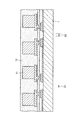
図13はこの発明の第2実施形態としてのネットワーク電子部品の等価回路的平面図を示す。このネットワーク電子部品では、平面正方形状のシリコン基板1上に1つの薄膜抵抗素子2と1つの薄膜容量素子(薄膜受動素子)31とからなるRC素子(ローパスフィルタ)が設けられている。この場合、薄膜抵抗素子2の両端部は、柱状電極からなる入力側および出力側の外部接続用電極32、33に接続されている。薄膜容量素子31の一端部は薄膜抵抗素子2の出力側に接続され、他端部は、柱状電極からなる入力側および出力側の外部接続用電極34、35に接続されている。
(Second Embodiment)
FIG. 13 is an equivalent circuit plan view of a network electronic component as a second embodiment of the present invention. In this network electronic component, an RC element (low-pass filter) composed of one thin film resistive element 2 and one thin film capacitive element (thin film passive element) 31 is provided on a planar square silicon substrate 1. In this case, both end portions of the thin film resistance element 2 are connected to the external connection electrodes 32 and 33 on the input side and the output side made of columnar electrodes. One end of the thin film capacitive element 31 is connected to the output side of the thin film resistive element 2, and the other end is connected to the external connection electrodes 34 and 35 on the input side and the output side made up of columnar electrodes.

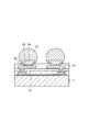
次に、図13に示す薄膜抵抗素子2の部分について、図13のXIV−XIV線に沿う断面図である図14を参照して説明する。図14に示すネットワーク電子部品において、図3に示すネットワーク電子部品と異なる点は、保護膜7と封止膜12との間にエポキシ系樹脂やポリイミド系樹脂等からなる層間絶縁膜41を設け、保護膜7の上面に設けられた銅等からなる下地金属層42を含む銅からなる中間配線43を絶縁膜5および保護膜7の開口部6、8を介して接続パッド4に接続させ、層間絶縁膜41の上面に設けられた下地金属層9を含む配線10を層間絶縁膜41に設けられた開口部44を介して中間配線43に接続させた点である。   Next, the thin film resistor element 2 shown in FIG. 13 will be described with reference to FIG. 14 which is a cross-sectional view taken along the line XIV-XIV in FIG. The network electronic component shown in FIG. 14 is different from the network electronic component shown in FIG. 3 in that an interlayer insulating film 41 made of an epoxy resin, a polyimide resin, or the like is provided between the protective film 7 and the sealing film 12. An intermediate wiring 43 made of copper including a base metal layer 42 made of copper or the like provided on the upper surface of the protective film 7 is connected to the connection pad 4 through the openings 6 and 8 of the insulating film 5 and the protective film 7, The wiring 10 including the base metal layer 9 provided on the upper surface of the insulating film 41 is connected to the intermediate wiring 43 through the opening 44 provided in the interlayer insulating film 41.

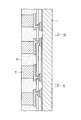
次に、図13に示す薄膜容量素子31の部分について、図13のXV−XV線に沿う断面図である図15を参照して説明する。保護膜7の上面には銅等からなる下地金属層45を含む銅からなる下層導電層46が設けられている。この場合、下地金属層45を含む下層導電層46は、図14に示す下地金属層42を含む中間配線43に引き回し線(図示せず)を介して接続されている。層間絶縁膜41の上面には銅等からなる下地金属層47を含む銅からなる上層導電層48が設けられている。   Next, the thin film capacitive element 31 shown in FIG. 13 will be described with reference to FIG. 15 which is a cross-sectional view taken along line XV-XV in FIG. A lower conductive layer 46 made of copper including a base metal layer 45 made of copper or the like is provided on the upper surface of the protective film 7. In this case, the lower conductive layer 46 including the base metal layer 45 is connected to the intermediate wiring 43 including the base metal layer 42 shown in FIG. 14 via a lead line (not shown). An upper conductive layer 48 made of copper including a base metal layer 47 made of copper or the like is provided on the upper surface of the interlayer insulating film 41.

ここで、上層導電層48と下層導電層46とは、その間に層間絶縁膜41が介在された状態で、相対向して配置され、薄膜容量素子31を構成している。上層導電層48は2つの接続パッド部を有し、これらの接続パッド部上面には柱状電極11が設けられている。上層導電層48を含む層間絶縁膜41の上面には封止膜12がその上面が柱状電極11の上面と面一となるように設けられている。柱状電極11の上面には半田ボール13が設けられている。   Here, the upper conductive layer 48 and the lower conductive layer 46 are disposed to face each other with the interlayer insulating film 41 interposed therebetween, and constitute the thin film capacitive element 31. The upper conductive layer 48 has two connection pad portions, and the columnar electrode 11 is provided on the upper surface of these connection pad portions. The sealing film 12 is provided on the upper surface of the interlayer insulating film 41 including the upper conductive layer 48 so that the upper surface thereof is flush with the upper surface of the columnar electrode 11. A solder ball 13 is provided on the upper surface of the columnar electrode 11.

そして、このネットワーク電子部品でも、シリコン基板1上にのみ外部接続用電極としての柱状電極11を設けているので、構造が簡単である。また、このネットワーク電子部品を製造する場合も、上記第1実施形態の場合と同様に、シリコン基板1上の複数のネットワーク電子部品形成領域に対して、薄膜抵抗体3、接続パッド4、中間配線43、下層導電層46、配線10、上層導電層48、柱状電極11および半田ボール13の形成を一括して行い、その後に分断して複数個のネットワーク電子部品を得ることができるので、製造工程を簡略化することができる。   Also in this network electronic component, since the columnar electrode 11 as the external connection electrode is provided only on the silicon substrate 1, the structure is simple. Also in the case of manufacturing this network electronic component, as in the case of the first embodiment, the thin film resistor 3, the connection pad 4, and the intermediate wiring are formed on the plurality of network electronic component forming regions on the silicon substrate 1. 43, the lower conductive layer 46, the wiring 10, the upper conductive layer 48, the columnar electrode 11 and the solder ball 13 can be collectively formed and then divided to obtain a plurality of network electronic components. Can be simplified.

(第3実施形態)
図16はこの発明の第3実施形態としてのネットワーク電子部品の等価回路的平面図を示す。このネットワーク電子部品では、シリコン基板1上に1つの薄膜抵抗素子2と2つの薄膜容量素子31が設けられている。この場合、薄膜抵抗素子2の両端部は、上側の2つの柱状電極11からなる外部接続用電極に接続されている。一方の薄膜容量素子31の両端部は、左側の2つの柱状電極11からなる外部接続用電極に接続されている。他方の薄膜容量素子31の両端部は、右側の2つの柱状電極11からなる外部接続用電極に接続されている。
(Third embodiment)
FIG. 16 is an equivalent circuit plan view of a network electronic component as a third embodiment of the present invention. In this network electronic component, one thin film resistive element 2 and two thin film capacitive elements 31 are provided on a silicon substrate 1. In this case, both ends of the thin film resistance element 2 are connected to an external connection electrode composed of the upper two columnar electrodes 11. Both end portions of one thin film capacitive element 31 are connected to an external connection electrode composed of two columnar electrodes 11 on the left side. Both end portions of the other thin film capacitive element 31 are connected to an external connection electrode composed of two columnar electrodes 11 on the right side.

(第4実施形態)
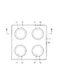
例えば、上記第1実施形態では、図4に示すダイシングストリート23の全てに沿って切断し、図1に示すように、平面正方形状で2つの薄膜抵抗素子2を有するネットワーク電子部品を複数個得ているが、これに限定されるものではない。例えば、図4において、縦線からなるダイシングストリート23の全てに沿って切断し、且つ、横線からなるダイシングストリート23の1本おきに沿って切断すると、図17に示すこの発明の第4実施形態のように、平面長方形状で4つの薄膜抵抗素子2を有するネットワーク電子部品が複数個得られる。
(Fourth embodiment)
For example, in the first embodiment, a plurality of network electronic components that are cut along all of the dicing streets 23 shown in FIG. 4 and have two thin film resistance elements 2 in a square shape as shown in FIG. 1 are obtained. However, it is not limited to this. For example, in FIG. 4, when cutting along all the dicing streets 23 consisting of vertical lines and cutting along every other dicing street 23 consisting of horizontal lines, the fourth embodiment of the present invention shown in FIG. As described above, a plurality of network electronic components having a rectangular plane shape and having four thin film resistor elements 2 are obtained.

(第5実施形態)
また、図4において、縦線からなるダイシングストリート23の1本おきに沿って切断し、且つ、横線からなるダイシングストリート23の1本おきに沿って切断すると、図18に示すこの発明の第5実施形態のように、平面正方形状で8つの薄膜抵抗素子2を有するネットワーク電子部品が複数個得られる。
(Fifth embodiment)
Further, in FIG. 4, when cutting along every other dicing street 23 consisting of vertical lines and cutting along every other dicing street 23 consisting of horizontal lines, the fifth embodiment of the present invention shown in FIG. As in the embodiment, a plurality of network electronic components having a square planar shape and having eight thin film resistor elements 2 are obtained.

ここで、上記第1、第4、第5実施形態から明らかなように、図4に示す同一のウエハ状態のシリコン基板1を切断するとき、ダイシング位置を変更するだけで、ネットワーク電子部品形成領域21が1つ含まれるように分断したり、ネットワーク電子部品形成領域21が2つあるいは4つつまり偶数含まれるように分断したりすることができる。このような切断を可能とするのは、上述の如く、ウエハ状態のシリコン基板1上の複数のネットワーク電子部品形成領域21に対して、薄膜抵抗体3、接続パッド4、配線10、柱状電極11および半田ボール13の形成を一括して行い、その後に分断しているからである。   Here, as is clear from the first, fourth, and fifth embodiments, when the silicon substrate 1 in the same wafer state shown in FIG. 4 is cut, the network electronic component forming region can be simply changed by changing the dicing position. It is possible to divide so that one 21 is included, or to divide so that two or four network electronic component forming regions 21 are included, that is, an even number. As described above, such cutting is possible with respect to the plurality of network electronic component forming regions 21 on the silicon substrate 1 in the wafer state, with respect to the thin film resistor 3, the connection pad 4, the wiring 10, and the columnar electrode 11. This is because the solder balls 13 are formed all at once and then divided.

(第6実施形態)
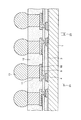
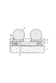
図19はこの発明の第6実施形態としてのネットワーク電子部品の断面図を示す。このネットワーク電子部品において、図3に示すネットワーク電子部品と異なる点は、半田ボール13の代わりに、柱状電極11の上面に半田層13aを設けた点である。
(Sixth embodiment)
FIG. 19 is a sectional view of a network electronic component as a sixth embodiment of the present invention. This network electronic component is different from the network electronic component shown in FIG. 3 in that a solder layer 13 a is provided on the upper surface of the columnar electrode 11 instead of the solder ball 13.

(第7実施形態)
図20はこの発明の第7実施形態としてのネットワーク電子部品の断面図を示す。このネットワーク電子部品において、図3に示すネットワーク電子部品と異なる点は、柱状電極11および封止膜11を有せず、配線10を含む保護膜7の上面にソルダーレジスト等からなるオーバーコート膜51を設け、配線10の接続パッド部に対応する部分におけるオーバーコート膜51に開口部52を設け、開口部52を介して露出された配線10の接続パッド部(外部接続用電極)上に半田ボールを設けた点である。
(Seventh embodiment)
FIG. 20 is a sectional view of a network electronic component as a seventh embodiment of the present invention. This network electronic component is different from the network electronic component shown in FIG. 3 in that the columnar electrode 11 and the sealing film 11 are not provided, and the overcoat film 51 made of a solder resist or the like is formed on the upper surface of the protective film 7 including the wiring 10. And an opening 52 is provided in the overcoat film 51 in a portion corresponding to the connection pad portion of the wiring 10, and a solder ball is formed on the connection pad portion (external connection electrode) of the wiring 10 exposed through the opening 52. This is the point.

(第8実施形態)
図21はこの発明の第8実施形態としてのネットワーク電子部品の断面図を示す。このネットワーク電子部品において、図20に示すネットワーク電子部品と異なる点は、オーバーコート膜51の開口部52内およびその近傍のオーバーコート膜51の上面に銅等からなる下地金属層53および銅からなる上層接続パッド(外部接続用電極)54を配線10の接続パッド部に接続させて設け、下地金属層53を含む上層接続パッド54上に半田ボール13を設けた点である。
(Eighth embodiment)
FIG. 21 is a sectional view of a network electronic component as an eighth embodiment of the present invention. This network electronic component is different from the network electronic component shown in FIG. 20 in that the base metal layer 53 made of copper or the like is formed on the upper surface of the overcoat film 51 in the vicinity of the opening 52 of the overcoat film 51 and copper. The upper layer connection pad (external connection electrode) 54 is provided so as to be connected to the connection pad portion of the wiring 10, and the solder ball 13 is provided on the upper layer connection pad 54 including the base metal layer 53.

この発明の第1実施形態としてのネットワーク電子部品の等価回路的平面図。The equivalent circuit top view of the network electronic component as 1st Embodiment of this invention. 図1に示すネットワーク電子部品の平面図。The top view of the network electronic component shown in FIG. 図2のIII−III線に沿う断面図。Sectional drawing which follows the III-III line | wire of FIG. 図1〜図3に示すネットワーク電子部品の製造に際し、当初用意したウエハ状態のシリコン基板の平面図。The top view of the silicon substrate of the wafer state initially prepared in the case of manufacture of the network electronic component shown in FIGS. 図4に続く工程の断面図。Sectional drawing of the process following FIG. 図5に続く工程の断面図。Sectional drawing of the process following FIG. 図6に続く工程の断面図。Sectional drawing of the process following FIG. 図7に続く工程の断面図。Sectional drawing of the process following FIG. 図8に続く工程の断面図。FIG. 9 is a cross-sectional view of the process following FIG. 8. 図9に続く工程の断面図。Sectional drawing of the process following FIG. 図10に続く工程の断面図。Sectional drawing of the process following FIG. 図11に続く工程の断面図。Sectional drawing of the process following FIG. この発明の第2実施形態としてのネットワーク電子部品の等価回路的平面図。The equivalent circuit top view of the network electronic component as 2nd Embodiment of this invention. 図13のXIV−XIV線に沿う断面図。Sectional drawing which follows the XIV-XIV line | wire of FIG. 図13のXV−XV線に沿う断面図。Sectional drawing which follows the XV-XV line | wire of FIG. この発明の第3実施形態としてのネットワーク電子部品の等価回路的平面図。The equivalent circuit top view of the network electronic component as 3rd Embodiment of this invention. この発明の第4実施形態としてのネットワーク電子部品の等価回路的平面図。The equivalent circuit top view of the network electronic component as 4th Embodiment of this invention. この発明の第5実施形態としてのネットワーク電子部品の等価回路的平面図。The equivalent circuit top view of the network electronic component as 5th Embodiment of this invention. この発明の第6実施形態としてのネットワーク電子部品の断面図。Sectional drawing of the network electronic component as 6th Embodiment of this invention. この発明の第7実施形態としてのネットワーク電子部品の断面図。Sectional drawing of the network electronic component as 7th Embodiment of this invention. この発明の第8実施形態としてのネットワーク電子部品の断面図。Sectional drawing of the network electronic component as 8th Embodiment of this invention.

符号の説明Explanation of symbols

1 シリコン基板
2 薄膜抵抗素子
3 薄膜抵抗体
4 接続パッド
5 絶縁膜
7 保護膜
10 配線
11 柱状電極
12 封止膜
13 半田ボール
DESCRIPTION OF SYMBOLS 1 Silicon substrate 2 Thin film resistive element 3 Thin film resistor 4 Connection pad 5 Insulating film 7 Protective film 10 Wiring 11 Columnar electrode 12 Sealing film 13 Solder ball

Claims (21)

基板と、前記基板上に設けられた薄膜受動素子と、前記薄膜受動素子を含む前記基板上に前記薄膜受動素子に接続されて設けられた複数の外部接続用電極とを有することを特徴とするネットワーク電子部品。   It has a substrate, a thin film passive element provided on the substrate, and a plurality of external connection electrodes provided on the substrate including the thin film passive element and connected to the thin film passive element. Network electronic components. 請求項1に記載の発明において、前記基板は半導体基板であることを特徴とするネットワーク電子部品。   2. The network electronic component according to claim 1, wherein the substrate is a semiconductor substrate. 請求項1に記載の発明において、前記薄膜受動素子は抵抗素子であることを特徴とするネットワーク電子部品。   2. The network electronic component according to claim 1, wherein the thin film passive element is a resistance element. 請求項1に記載の発明において、前記薄膜受動素子は容量素子であることを特徴とするネットワーク電子部品。   2. The network electronic component according to claim 1, wherein the thin film passive element is a capacitive element. 請求項1に記載の発明において、前記薄膜受動素子はRC素子であることを特徴とするネットワーク電子部品。   2. The network electronic component according to claim 1, wherein the thin film passive element is an RC element. 請求項1に記載の発明において、前記薄膜受動素子は複数であることを特徴とするネットワーク電子部品。   2. The network electronic component according to claim 1, wherein a plurality of the thin film passive elements are provided. 請求項1に記載の発明において、前記外部接続用電極は、前記薄膜受動素子を含む前記基板上に前記薄膜受動素子に接続されて設けられた配線の接続パッド部上に設けられた柱状電極であることを特徴とするネットワーク電子部品。   2. The external connection electrode according to claim 1, wherein the external connection electrode is a columnar electrode provided on a connection pad portion of a wiring provided on the substrate including the thin film passive element and connected to the thin film passive element. A network electronic component characterized by being. 請求項1に記載の発明において、前記外部接続用電極は、前記薄膜受動素子を含む前記基板上に前記薄膜受動素子に接続されて設けられた配線の接続パッド部であることを特徴とするネットワーク電子部品。   2. The network according to claim 1, wherein the external connection electrode is a connection pad portion of a wiring provided on the substrate including the thin film passive element and connected to the thin film passive element. Electronic components. 請求項1に記載の発明において、前記外部接続用電極は、前記薄膜受動素子を含む前記基板上に前記薄膜受動素子に接続されて設けられた配線の接続パッド部上に設けられた上層接続パッドであることを特徴とするネットワーク電子部品。   2. The external connection electrode according to claim 1, wherein the external connection electrode is provided on a connection pad portion of a wiring provided on the substrate including the thin film passive element and connected to the thin film passive element. A network electronic component characterized by being. 請求項1に記載の発明において、前記外部接続用電極上に半田ボールが設けられていることを特徴とするネットワーク電子部品。   2. The network electronic component according to claim 1, wherein a solder ball is provided on the external connection electrode. 請求項1に記載の発明において、前記外部接続用電極上に半田層が設けられていることを特徴とするネットワーク電子部品。   2. The network electronic component according to claim 1, wherein a solder layer is provided on the external connection electrode. ウエハ状態の半導体基板上の複数のネットワーク電子部品形成領域にそれぞれ薄膜受動素子を形成する工程と、前記薄膜受動素子を含む前記ウエハ状態の半導体基板上の前記各ネットワーク電子部品形成領域にそれぞれ外部接続用電極を対応する前記薄膜受動素子に接続されて形成する工程と、前記ウエハ状態の半導体基板を切断して少なくとも1つのネットワーク電子部品形成領域を有するネットワーク電子部品を複数個得る工程とを有することを特徴とするネットワーク電子部品の製造方法。   Forming a thin film passive element in each of a plurality of network electronic component forming regions on a semiconductor substrate in a wafer state, and external connection to each of the network electronic component forming regions on the semiconductor substrate in the wafer state including the thin film passive device And forming a plurality of network electronic components having at least one network electronic component forming region by cutting the semiconductor substrate in the wafer state. A method for manufacturing a network electronic component characterized by the above. 請求項12に記載の発明において、前記薄膜受動素子は抵抗素子であることを特徴とするネットワーク電子部品の製造方法。   13. The method of manufacturing a network electronic component according to claim 12, wherein the thin film passive element is a resistance element. 請求項12に記載の発明において、前記薄膜受動素子は容量素子であることを特徴とするネットワーク電子部品の製造方法。   13. The method of manufacturing a network electronic component according to claim 12, wherein the thin film passive element is a capacitive element. 請求項12に記載の発明において、前記薄膜受動素子はRC素子であることを特徴とするネットワーク電子部品の製造方法。   13. The method of manufacturing a network electronic component according to claim 12, wherein the thin film passive element is an RC element. 請求項12に記載の発明において、前記切断は、前記ネットワーク電子部品形成領域が偶数含まれるように切断することを特徴とするネットワーク電子部品の製造方法。   13. The method for manufacturing a network electronic component according to claim 12, wherein the cutting is performed so that the network electronic component forming region is evenly included. 請求項12に記載の発明において、前記外部接続用電極は、前記薄膜受動素子を含む前記基板上に前記薄膜受動素子に接続されて設けられた配線の接続パッド部上に設けられた柱状電極であることを特徴とするネットワーク電子部品の製造方法。   The invention according to claim 12, wherein the external connection electrode is a columnar electrode provided on a connection pad portion of a wiring provided connected to the thin film passive element on the substrate including the thin film passive element. A method for manufacturing a network electronic component, comprising: 請求項12に記載の発明において、前記外部接続用電極は、前記薄膜受動素子を含む前記基板上に前記薄膜受動素子に接続されて設けられた配線の接続パッド部であることを特徴とするネットワーク電子部品の製造方法。   13. The network according to claim 12, wherein the external connection electrode is a connection pad portion of a wiring provided to be connected to the thin film passive element on the substrate including the thin film passive element. Manufacturing method of electronic components. 請求項12に記載の発明において、前記外部接続用電極は、前記薄膜受動素子を含む前記基板上に前記薄膜受動素子に接続されて設けられた配線の接続パッド部上に設けられた上層接続パッドであることを特徴とするネットワーク電子部品の製造方法。   13. The external connection electrode according to claim 12, wherein the external connection electrode is provided on a connection pad portion of a wiring provided on the substrate including the thin film passive element and connected to the thin film passive element. A method of manufacturing a network electronic component, wherein 請求項12に記載の発明において、前記外部接続用電極上に半田ボールを形成する工程を有することを特徴とするネットワーク電子部品の製造方法。   13. The method of manufacturing a network electronic component according to claim 12, further comprising a step of forming a solder ball on the external connection electrode. 請求項12に記載の発明において、前記外部接続用電極上に半田層を形成する工程を有することを特徴とするネットワーク電子部品の製造方法。
13. The method of manufacturing a network electronic component according to claim 12, further comprising a step of forming a solder layer on the external connection electrode.
JP2004107800A 2004-03-31 2004-03-31 Network electronic component and manufacturing method thereof Pending JP2005294548A (en)

Priority Applications (2)

Application Number Priority Date Filing Date Title
JP2004107800A JP2005294548A (en) 2004-03-31 2004-03-31 Network electronic component and manufacturing method thereof
US11/093,571 US7808073B2 (en) 2004-03-31 2005-03-30 Network electronic component, semiconductor device incorporating network electronic component, and methods of manufacturing both

Applications Claiming Priority (1)

Application Number Priority Date Filing Date Title
JP2004107800A JP2005294548A (en) 2004-03-31 2004-03-31 Network electronic component and manufacturing method thereof

Publications (1)

Publication Number Publication Date
JP2005294548A true JP2005294548A (en) 2005-10-20

Family

ID=35327138

Family Applications (1)

Application Number Title Priority Date Filing Date
JP2004107800A Pending JP2005294548A (en) 2004-03-31 2004-03-31 Network electronic component and manufacturing method thereof

Country Status (1)

Country Link
JP (1) JP2005294548A (en)

Cited By (1)

* Cited by examiner, † Cited by third party
Publication number Priority date Publication date Assignee Title
JP2008108935A (en) * 2006-10-26 2008-05-08 Casio Comput Co Ltd Manufacturing method of semiconductor device

Cited By (1)

* Cited by examiner, † Cited by third party
Publication number Priority date Publication date Assignee Title
JP2008108935A (en) * 2006-10-26 2008-05-08 Casio Comput Co Ltd Manufacturing method of semiconductor device

Similar Documents

Publication Publication Date Title
US7022609B2 (en) Manufacturing method of a semiconductor substrate provided with a through hole electrode
US7782173B2 (en) Chip resistor
JP4716099B2 (en) Manufacturing method of chip-type fuse
US7999189B2 (en) Circuit board structure and method for fabricating the same
JP6606331B2 (en) Electronic equipment
CN106898448B (en) Chip resistor and its manufacturing method
JP2005175019A (en) Semiconductor device and multilayer semiconductor device
CN104718802A (en) The printed circuit board and the method for manufacturing the same
JP2004214646A (en) Low-loss/high-density array interconnection
JP6021441B2 (en) Semiconductor device
JP2006344477A (en) Chip type fuse
JP4752280B2 (en) Chip-type electronic component and manufacturing method thereof
JP3945380B2 (en) Semiconductor device and manufacturing method thereof
US20170318684A1 (en) Method of manufacturing wiring board and wiring board
US9236336B2 (en) Systems and methods for mitigation of mechanical degradation in high performance electrical circuit packages
TWI517318B (en) Substrate having pillar group and semiconductor package having pillar group
CN106356361A (en) Semiconductor device and method of manufacturing the same
JP4592413B2 (en) Circuit equipment
JP2005294548A (en) Network electronic component and manufacturing method thereof
JP5137320B2 (en) Semiconductor device and manufacturing method thereof
JP2006196811A (en) Capacitor and composite parts using the same
JP2009016793A (en) Apertured chip resistor and method for fabricating the same
JP2010062170A (en) Semiconductor device and manufacturing method thereof
CN112490197A (en) Semiconductor device package and method of manufacturing the same
TW201117334A (en) Semiconductor device and manufacturing method thereof

Legal Events

Date Code Title Description
RD02 Notification of acceptance of power of attorney

Free format text: JAPANESE INTERMEDIATE CODE: A7422

Effective date: 20060209

RD04 Notification of resignation of power of attorney

Free format text: JAPANESE INTERMEDIATE CODE: A7424

Effective date: 20060314

A977 Report on retrieval

Free format text: JAPANESE INTERMEDIATE CODE: A971007

Effective date: 20071019

A131 Notification of reasons for refusal

Free format text: JAPANESE INTERMEDIATE CODE: A131

Effective date: 20071030

A521 Written amendment

Free format text: JAPANESE INTERMEDIATE CODE: A523

Effective date: 20071226

A02 Decision of refusal

Free format text: JAPANESE INTERMEDIATE CODE: A02

Effective date: 20080129