JP2005294450A - Position measuring method, exposure method and apparatus, and device manufacturing method - Google Patents
Position measuring method, exposure method and apparatus, and device manufacturing method Download PDFInfo
- Publication number
- JP2005294450A JP2005294450A JP2004105914A JP2004105914A JP2005294450A JP 2005294450 A JP2005294450 A JP 2005294450A JP 2004105914 A JP2004105914 A JP 2004105914A JP 2004105914 A JP2004105914 A JP 2004105914A JP 2005294450 A JP2005294450 A JP 2005294450A
- Authority
- JP
- Japan
- Prior art keywords
- mark
- reticle
- light
- wafer
- signal
- Prior art date
- Legal status (The legal status is an assumption and is not a legal conclusion. Google has not performed a legal analysis and makes no representation as to the accuracy of the status listed.)
- Pending
Links
Images
Landscapes
- Length Measuring Devices By Optical Means (AREA)
- Exposure And Positioning Against Photoresist Photosensitive Materials (AREA)
- Exposure Of Semiconductors, Excluding Electron Or Ion Beam Exposure (AREA)
Abstract
【課題】下地表面にゴミが存在しても影響を受けることなく適切に下地波形の光量依存成分を検出し、下地波形による補正を適切に行い、レチクル等の位置を高精度に計測する位置計測方法を提供することにある。
【解決手段】下地波形の光量依存成分を検出する方法として、その下地のマークが形成されていない領域(非マーク領域)に光ビームを照射し、その反射ビームを観察系を介して撮像し、その撮像信号に基づいて光量依存成分を検出する。光ビームを非マーク領域に照射して計測する際には、照射対象の領域の表面に対してデフォーカスした状態で表面検出を行う。表面にゴミの付着や欠陥の発生があったとしても、デフォーカスした状態なので、下地波形にノイズとして取り込まれることも防ぐことができ、ゴミや欠陥の影響のない適切な光量依存成分を検出することができる。
【選択図】 図7[PROBLEMS] To detect a light amount-dependent component of a ground waveform appropriately without being affected even if dust is present on the ground surface, appropriately correct the ground waveform, and accurately measure the position of a reticle or the like. It is to provide a method.
As a method for detecting a light amount-dependent component of a ground waveform, a light beam is irradiated to a region where the ground mark is not formed (non-marked region), and the reflected beam is imaged through an observation system. A light quantity dependent component is detected based on the imaging signal. When the measurement is performed by irradiating the non-mark region with the light beam, surface detection is performed in a state where the surface of the irradiation target region is defocused. Even if dust is attached to the surface or a defect is generated, it is in a defocused state, so that it can be prevented from being taken in as noise in the ground waveform, and an appropriate light quantity dependent component that is not affected by dust or a defect is detected. be able to.
[Selection] Figure 7
Description
本発明は、半導体素子等の電子デバイスを製造する際のリソグラフィー工程で用いる露光装置に適用して好適な、基板あるいはマスクの位置を計測する位置計測方法、その位置計測方法を用いる露光方法とその装置、及び、その露光方法を用いたデバイス製造方法に関する。 The present invention relates to a position measurement method for measuring the position of a substrate or a mask, an exposure method using the position measurement method, and an exposure method suitable for being applied to an exposure apparatus used in a lithography process when manufacturing an electronic device such as a semiconductor element. The present invention relates to an apparatus and a device manufacturing method using the exposure method.
半導体素子、液晶表示素子、CCD等の撮像素子、プラズマディスプレイ素子、薄膜磁気ヘッド等の電子デバイス(以下、電子デバイスと総称する)の製造にあたっては、露光装置を用いて、フォトマスクやレチクル(以下、レチクルと総称する)に形成された微細なパターンの像を、フォトレジスト等の感光剤を塗布した半導体ウエハやガラスプレート等の基板(以下、ウエハと称する)上に投影露光する。その際、レチクルとウエハとを高精度に位置合わせ(アライメント)し、レチクルのパターンをウエハ上のパターンに高精度に重ね合わせる必要がある。近年、パターンの微細化や高集積度化が急速に進んでおり、このような露光装置には以前に増して高い露光精度が要求されている。そのため、アライメントに対する精度の要求も一層厳しくなってきており、より高精度なアライメントが要望されている。 In the manufacture of electronic devices such as semiconductor devices, liquid crystal display devices, CCD imaging devices, plasma display devices, thin film magnetic heads and the like (hereinafter collectively referred to as electronic devices), an exposure apparatus is used to manufacture photomasks and reticles (hereinafter referred to as electronic devices). The image of the fine pattern formed on the reticle is generally projected and exposed onto a substrate (hereinafter referred to as a wafer) such as a semiconductor wafer or a glass plate coated with a photosensitive agent such as a photoresist. At that time, it is necessary to align the reticle and the wafer with high accuracy and to superimpose the reticle pattern on the pattern on the wafer with high accuracy. In recent years, pattern miniaturization and high integration are rapidly progressing, and such exposure apparatuses are required to have higher exposure accuracy than before. For this reason, the demand for accuracy for alignment is becoming stricter, and higher-precision alignment is demanded.
ウエハの位置計測は、ウエハ上に形成された位置合わせマーク(アライメントマーク)の位置を計測することにより行われる。このアライメントマークの位置を計測するアライメント系として、例えばハロゲンランプ等を光源とする波長帯域幅の広い光でマークを照射し、反射光をCCDカメラなどで撮像し、得られたアライメントマークの画像データを画像処理してマーク位置を計測するFIA(Field Image Alignment)系のオフアクシス・アライメントセンサなどが知られている。このFIA系のアライメントセンサによると、レジスト層による薄膜干渉の影響を受けにくくなり、アルミマークや非対称マーク等についても高精度な位置検出が可能である。 Wafer position measurement is performed by measuring the position of an alignment mark (alignment mark) formed on the wafer. As an alignment system for measuring the position of the alignment mark, for example, the mark is irradiated with light having a wide wavelength bandwidth using a halogen lamp or the like as a light source, and the reflected light is imaged with a CCD camera or the like. An FIA (Field Image Alignment) type off-axis alignment sensor that measures a mark position by image processing is known. According to this FIA-based alignment sensor, it is difficult to be affected by the thin film interference caused by the resist layer, and it is possible to detect the position of an aluminum mark or an asymmetric mark with high accuracy.
レチクルの位置検出も、ウエハの位置検出と同様にレチクルに形成された位置合わせマーク(アライメントマーク)を検出することにより行われるが、この場合には、検出光束として露光光を用いるものが一般的である。例えば、露光光をレチクル上に形成されたアライメントマークに照射し、反射光をCCDカメラなどで撮像し、得られたアライメントマークの画像データを画像処理してマーク位置を計測するVRA(VisualReticle Alignment)方式のセンサなどが知られている。このようなレチクルアライメント系においては、ウエハステージにある(固設された)基準板上にパターニングされているウエハ基準マーク(ウエハフィデュシャルマーク)と、レチクル上にパターニングされたレチクルアライメントマークをカメラで撮像し、得られた信号に基づいてウエハ基準マークとレチクルアライメントマークの相対位置を求め、これに基づいてレチクルの位置合わせを行っている。 Like the wafer position detection, the reticle position is also detected by detecting an alignment mark (alignment mark) formed on the reticle. In this case, the exposure light is generally used as a detection light beam. It is. For example, VRA (Visual Reticle Alignment) that irradiates alignment light formed on a reticle with exposure light, images reflected light with a CCD camera, etc., and processes the image data of the obtained alignment mark to measure the mark position. A sensor of the type is known. In such a reticle alignment system, a wafer reference mark (wafer fiducial mark) patterned on a reference plate (fixed) on a wafer stage and a reticle alignment mark patterned on the reticle are displayed on the camera. The relative position between the wafer reference mark and the reticle alignment mark is obtained based on the obtained signal, and the reticle is aligned based on the relative position.
ところで、上述したようなアライメント系においては、カメラの暗電流むら及びピクセル間の感度ばらつき、あるいは、センサのカバーガラス及び光学系等で発生する干渉縞等により、計測結果にいわゆるだまされ(すなわち誤差)が生じる場合がある。このだまされを解消するために、通常、下地補正と称する処理を施すことが提案されている。下地補正とは、暗電流むら等の光量非依存成分、及び、干渉縞等の光量依存成分を各々予め計測して下地波形(下地信号)として記憶しておき、ウエハ基準マークやレチクルアライメントマークの信号波形(マーク信号)を検出した時に、得られた信号波形を下地波形を参照して補正する処理である。具体的には、例えば、得られた信号波形から光量非依存成分を減じ、その結果を実質的な光量依存成分で除する等の処理により、計測結果の信号波形を補正する(例えば、特許文献1参照)。
上述したような下地補正を行う場合、その光量依存成分の計測は、レチクル及びウエハステージの基準板等のマークが形成されていない非マーク領域(下地領域)を照明し、その反射戻り光を通常のマーク検出時と同様にアライメント系の光学系及び撮像系を通過させ、その時に観察される信号波形を検出することにより行う。 When the background correction as described above is performed, the measurement of the light amount dependent component is performed by illuminating a non-mark area (background area) where a mark such as a reticle and a wafer stage reference plate is not formed, and the reflected return light is usually used. As in the case of the mark detection, the optical system and the imaging system of the alignment system are passed, and the signal waveform observed at that time is detected.
この時、例えば基準板上の下地領域の表面にゴミや欠陥が存在すると、これがアライメント系により観察され、ノイズを含む不適切な光量依存成分を計測してしまうという問題が生じる。観察した信号波形を、そのようなノイズを含む光量依存成分に基づいて補正すると、補正結果の信号波形にノイズに対応する波形が出現することになる。そして、特にそのノイズによる波形が本来のマークパターンに対応する波形の近傍に出現した場合には、位置計測結果は誤差を含んだ、いわゆるだまされが生じた結果となる可能性が高く、位置合わせ精度を低下させる可能性がある。 At this time, for example, if dust or a defect exists on the surface of the base region on the reference plate, this is observed by the alignment system, and there is a problem that an inappropriate light amount dependent component including noise is measured. When the observed signal waveform is corrected based on the light quantity dependent component including such noise, a waveform corresponding to the noise appears in the signal waveform of the correction result. In particular, when the waveform due to the noise appears in the vicinity of the waveform corresponding to the original mark pattern, the position measurement result is likely to be a result of so-called fraud that includes an error. May reduce accuracy.
また、レチクルアライメント系においては、アライメントの際、照明ビームを投影光学系に入射させるために、投影光学系130の上部(レチクルアライメント系の光路上)に落射ミラー214が投入される。この落射ミラーは、露光光が投影光学系に供給される時には、露光光の光路外の退避位置に移動される。この落射ミラーの投入精度により、レチクルアライメント系においては、カメラ視野に対してアライメントマークがずれて計測される場合がある。そして、このような状況で、さらに上述したような光量依存成分の検出処理の際の下地領域のゴミや欠陥に基づくノイズが本来のマークパターンの波形の近傍に出現した場合には、位置計測結果は、いわゆるだまされが生じた結果、すなわち誤差を含んだ結果となる可能性が高くなり、位置合わせ精度を低下させる可能性が一層高くなる。
In the reticle alignment system, an
本発明はこのような課題に鑑みてなされたものであって、その目的は、下地表面にノイズや欠陥が生じた場合でも影響を受けることなく適切に下地波形の光量依存成分を検出することができ、下地波形による補正を適切に行い、レチクルやウエハ等に形成されたマークの位置を高精度に計測することのできる位置計測方法を提供することにある。 The present invention has been made in view of such problems, and its purpose is to appropriately detect the light amount-dependent component of the ground waveform without being affected even when noise or a defect occurs on the ground surface. Another object of the present invention is to provide a position measuring method capable of measuring the position of a mark formed on a reticle, a wafer or the like with high accuracy by appropriately performing correction based on a background waveform.
また、本発明の他の目的は、そのような位置計測方法を用いてレチクル(マスク)上に形成されたパターンを高精度に位置合わせして基板上に転写することのできる露光方法及び露光装置を提供することにある。 Another object of the present invention is to provide an exposure method and an exposure apparatus capable of aligning a pattern formed on a reticle (mask) with such a position measurement method with high accuracy and transferring the pattern onto a substrate. Is to provide.
また、本発明の他の目的は、そのような露光方法を用いることにより、高性能なデバイスを製造することのできるデバイス製造方法を提供することにある。 Another object of the present invention is to provide a device manufacturing method capable of manufacturing a high-performance device by using such an exposure method.
前記課題を解決するために、本発明に係る位置計測方法は、物体上に形成されたマークに光ビームを照射して該マークからの反射ビームを観察系を介して受光し、予め検出した光量依存成分を含む下地信号に基づいて前記受光して得たマーク信号を補正して補正マーク信号を求め、該補正マーク信号に基づいて前記マークの位置を計測する位置計測方法であって、前記マークが形成されている前記物体上のパターン形成面上であって、且つ該マークの存在しない領域である下地領域を、前記観察系の観察視野内に配置する第1工程と、前記下地領域上の前記光ビームの入射側に該光ビームを透過する物質層が存在する場合には、前記物質層の前記光ビーム入射側の表面に対して前記観察系がデフォーカスした状態下で前記下地領域を検出し、前記下地領域上に前記物質層が存在しない場合には、該下地領域の表面に対して該観察系がデフォーカスした状態下で該下地領域を検出する第2工程と、前記第2工程での検出結果に基づいて、前記光量依存成分を検出する第3工程とを有することを特徴とする。 In order to solve the above-described problem, the position measurement method according to the present invention irradiates a mark formed on an object with a light beam, receives a reflected beam from the mark through an observation system, and detects a light amount detected in advance. A position measurement method for correcting a mark signal obtained by receiving light based on a background signal including a dependent component to obtain a correction mark signal, and measuring the position of the mark based on the correction mark signal. A first step of disposing a ground region on the pattern forming surface on the object on which the mark is formed and in which the mark is not present within an observation field of view of the observation system; and on the ground region When there is a material layer that transmits the light beam on the incident side of the light beam, the base region is formed under a state where the observation system is defocused with respect to the surface of the material layer on the light beam incident side. Detect When the material layer does not exist on the ground region, a second step of detecting the ground region in a state where the observation system is defocused with respect to the surface of the ground region; and And a third step of detecting the light quantity dependent component based on a detection result.
このような位置検出方法においては、予め下地波形の光量依存成分を検出する方法として、その下地のマークが形成されていない領域(下地領域、非マーク領域)に光ビームを照射し、その反射ビームを観察系を介して撮像し、その撮像信号に基づいて光量依存成分を検出することとしている。そして、特に、下地領域上の光ビームの入射側に光ビームを透過する物質層が存在する場合には、その物質層の光ビーム入射側の表面に対してデフォーカスした状態で観察系が下地領域を検出し、下地領域上に物質層が存在しない場合には下地領域の表面に対してデフォーカスした状態で観察系が下地領域を検出するようにしている。従って、仮に非マーク領域を含む部材の表面にゴミの付着や欠陥の発生があったとしても、それらはデフォーカスした状態なので、ゴミや欠陥を識別できる形で取り込むことを回避することができ、これが下地波形にノイズとして取り込まれることを防ぐことができる。すなわち、ゴミや欠陥の影響のない適切な光量依存成分を検出することができる。 In such a position detection method, as a method for detecting the light amount-dependent component of the background waveform in advance, a light beam is irradiated to an area where the background mark is not formed (background area, non-mark area), and the reflected beam Is captured through the observation system, and the light quantity dependent component is detected based on the image signal. In particular, when there is a material layer that transmits a light beam on the incident side of the light beam on the ground region, the observation system is defocused on the surface of the material layer on the light beam incident side. The region is detected, and when the material layer does not exist on the base region, the observation system detects the base region in a defocused state with respect to the surface of the base region. Therefore, even if dust adheres to the surface of a member including a non-marked area or a defect occurs, it is in a defocused state, so that it is possible to avoid capturing dust and defects in an identifiable manner. This can be prevented from being taken in as noise in the background waveform. That is, it is possible to detect an appropriate light amount dependent component that is not affected by dust and defects.
また本発明に係る他の位置計測方法は、物体上に形成されたマークに光ビームを照射して該マークからの反射ビームを観察系を介して受光し、予め検出した光量依存成分を含む下地信号に基づいて前記受光して得たマーク信号を補正して補正マーク信号を求め、該補正マーク信号に基づいて前記マークの位置を計測する位置計測方法であって、前記マークが形成されている前記物体上のパターン形成面上であって、且つ該マークの存在しない領域である下地領域を、前記観察系の観察視野内に配置する第1工程と、前記下地領域に対して前記光ビームを照射した状態で、前記パターン形成面と平行な面に沿って該下地領域と該光ビームとを相対的に移動させながら、前記下地領域からの反射ビームを前記観察系を介して受光する第2工程と、前記第2工程で受光した信号に基づいて、前記光量依存成分を検出する第3工程とを有することを特徴とする。 According to another position measurement method of the present invention, a mark formed on an object is irradiated with a light beam, a reflected beam from the mark is received through an observation system, and a ground including a light quantity dependent component detected in advance is received. A position measurement method for correcting a mark signal obtained by receiving light based on a signal to obtain a correction mark signal and measuring the position of the mark based on the correction mark signal, wherein the mark is formed A first step of disposing a ground region on the pattern forming surface on the object and in which the mark is not present within an observation field of view of the observation system; and the light beam to the ground region A second light beam that receives a reflected beam from the ground region via the observation system while relatively moving the ground region and the light beam along a plane parallel to the pattern forming surface in the irradiated state. Process, Serial based on the second signal received by the step, characterized in that a third step of detecting the light intensity-dependent component.
好適には、前記第2工程では、前記物体の位置を規定するX軸及びY軸の両方に対して交差する方向に、前記下地領域と前記光ビームとを相対的に移動させることを特徴とする。 Preferably, in the second step, the base region and the light beam are relatively moved in a direction intersecting with both the X axis and the Y axis that define the position of the object. To do.
また、本発明に係る他の位置計測方法は、基板を載置する基板ステージ上に固設された第1基準部材上に形成された第1基準マーク、及びマスクステージ上に載置されたマスク上に形成されたマスクマークに光ビームを照射し、前記各マークからの反射ビームを観察系を介して受光し、予め検出した光量依存成分を含む下地信号に基づいて前記受光して得た信号を補正して補正マーク信号を求め、該補正マーク信号に基づいて前記マークの位置を計測する位置計測方法であって、前記マスク上のパターン形成面上であり且つ前記マスクマーク又はパターンの存在しない領域である第1下地領域、あるいは前記マスクステージ上に固設され第2基準マークを備えた第2基準部材上の基準パターン形成面上の該第2基準マークの存在しない領域である第2下地領域を、前記観察系の観察視野内に配置する第1工程と、前記第1下地領域又は前記第2下地領域からの反射ビームを前記観察系を介して受光する第2工程と、前記第2工程で受光した信号に基づいて、前記光量依存成分を検出する第3工程とを有することを特徴とする。 In addition, another position measuring method according to the present invention includes a first reference mark formed on a first reference member fixed on a substrate stage on which a substrate is placed, and a mask placed on the mask stage. A signal obtained by irradiating the mask mark formed above with a light beam, receiving a reflected beam from each mark through an observation system, and receiving the light based on a ground signal including a light quantity dependent component detected in advance. Is a position measurement method for determining a correction mark signal and measuring the position of the mark based on the correction mark signal, on the pattern forming surface on the mask and without the mask mark or pattern A first base region that is a region, or a region where the second reference mark does not exist on a reference pattern forming surface on a second reference member provided on the mask stage and provided with a second reference mark. And a second step of receiving a reflected beam from the first base region or the second base region via the observation system, and a second step of arranging the second base region in the observation field of view of the observation system. And a third step of detecting the light quantity dependent component based on the signal received in the second step.
また、本発明に係る露光方法は、マスク上に形成されたパターンを基板上に転写する露光方法であって、前記マスク又は前記基板の少なくとも何れか一方について、上述の何れかの位置計測方法により位置を計測し、当該計測結果に基づいて前記マスク又は前記基板の位置決めを行うことを特徴とする。 An exposure method according to the present invention is an exposure method for transferring a pattern formed on a mask onto a substrate, and at least one of the mask and the substrate is subjected to any one of the position measurement methods described above. The position is measured, and the mask or the substrate is positioned based on the measurement result.
また、本発明に係る露光装置は、マスク上に形成されたパターンを基板上に転写する露光装置であって、上述の何れかの位置計測方法により前記マスク又は前記基板の少なくとも何れか一方の位置を計測する位置計測手段を有することを特徴とする。 An exposure apparatus according to the present invention is an exposure apparatus for transferring a pattern formed on a mask onto a substrate, and the position of at least one of the mask and the substrate is determined by any one of the position measurement methods described above. It has the position measuring means which measures this.
また、本発明に係るデバイス製造方法は、上述の露光方法を用いて、マスク上に形成されたデバイスパターンを基板上に転写する工程を含むことを特徴とする。 A device manufacturing method according to the present invention includes a step of transferring a device pattern formed on a mask onto a substrate using the exposure method described above.
本発明によれば、下地表面にノイズや欠陥が生じた場合でも影響を受けることなく適切に下地波形の光量依存成分を検出することができ、下地波形による補正を適切に行い、レチクルやウエハ等に形成されたマークの位置を高精度に計測することのできる位置計測方法を提供することができる。 According to the present invention, it is possible to appropriately detect the light amount-dependent component of the base waveform without being affected even when noise or a defect occurs on the base surface, and to appropriately perform correction based on the base waveform, such as a reticle or wafer. It is possible to provide a position measuring method capable of measuring the position of the mark formed on the substrate with high accuracy.
また、そのような位置計測方法を用いてレチクル(マスク)上に形成されたパターンを高精度に位置合わせして基板上に転写することのできる露光方法及び露光装置を提供することができる。 Further, it is possible to provide an exposure method and an exposure apparatus capable of aligning and transferring a pattern formed on a reticle (mask) with high accuracy using such a position measurement method onto a substrate.
また、そのような露光方法を用いることにより、高性能なデバイスを製造することのできるデバイス製造方法を提供することができる。 In addition, by using such an exposure method, a device manufacturing method capable of manufacturing a high-performance device can be provided.
第1実施形態
本発明の第1実施形態について、図1〜図9を参照して説明する。
First Embodiment A first embodiment of the present invention will be described with reference to FIGS.
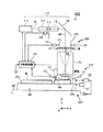
図1は、本実施形態に係る電子デバイス製造用の投影露光装置の概略構成を示す図である。図1に示す露光装置100は、マスクとしてのレチクルRと基板としてのウエハWとを1次元方向(図1ではY方向)に同期移動させつつレチクルRに形成された回路パターンをウエハW上に規定される各ショット領域に転写する、ステップ・アンド・スキャン方式の走査型露光装置(スキャニング・ステッパ)である。 FIG. 1 is a diagram showing a schematic configuration of a projection exposure apparatus for manufacturing an electronic device according to the present embodiment. 1 exposes a circuit pattern formed on a reticle R on a wafer W while synchronously moving a reticle R as a mask and a wafer W as a substrate in a one-dimensional direction (Y direction in FIG. 1). This is a step-and-scan type scanning exposure apparatus (scanning stepper) that transfers to each defined shot area.
まず、露光装置100の全体構成について説明する。
First, the overall configuration of the
露光装置100は、照明系110、レチクルステージ120、投影光学系130、ウエハステージ部140、レチクルアライメント系180、ウエハアライメントセンサ170、メインフォーカス系150及び主制御装置160を有する。
The
照明系110は、例えばエキシマレーザからなる光源111、ビーム整形用レンズ及びオプチカルインテグレータ(フライアイレンズ)等を含む照度均一化光学系112、照明系開口絞り板113(レボルバ)113、レボルバ駆動系114、リレー光学系116、図示しないレチクルブラインド、折り曲げミラー117、及び、図示しないコンデンサレンズ等を有する。
The
照明系110において、光源111から、例えばKrFエキシマレーザ光あるいはArFエキシマレーザ光等の照明ビームILが射出される。光源111におけるレーザパルスの発光は、主制御装置160により制御される。なお、光源111としては、超高圧水銀ランプを用いてもよい。その場合は、g線、i線等の紫外域の輝線が照明ビームILとして用いられる。
In the
光源111から射出された照明ビームILは、照度均一化光学系112により光束が一様化され、スペックルの低減化等が行われる。
The illumination beam IL emitted from the light source 111 is made uniform by the illuminance uniformizing
照度均一化光学系112の出口部分には、円板状部材からなる照明系開口絞り板113が配置されている。
An illumination system
照明系開口絞り板113には、ほぼ等角度間隔で、例えば、通常の円形開口の開口絞り、コヒーレンスファクタであるσ値を小さくするための小さな円形開口の開口絞り、輪帯照明用の輪帯状の開口絞り、及び、変形光源法用の複数の開口を偏心させて配置した変形開口絞り等の複数の開口絞りが配置されている。照明系開口絞り板113は、主制御装置160により制御されるモータ等のレボルバ駆動系114により回転駆動されるようになっており、これにより、何れかの開口絞りが照明ビームILの光路上に選択的に配置される。
The illumination system
照明系開口絞り板113の後段には、図示しないレチクルブラインドを介在してリレー光学系116が配置されている。レチクルブラインドの設置面は、レチクルRと共役関係にあり、このレチクルブラインドによりレチクルR上の照明ビームILにより照明される領域が規定される。
A relay optical system 116 is disposed behind the illumination system
リレー光学系116の後段には、リレー光学系116を通過した照明ビームILをレチクルRに向けて反射する折り曲げミラー117が配置され、この折り曲げミラー117のさらに後段(反射された照明ビームILの光路上の後段)に、図示しないコンデンサレンズが配置される。 A folding mirror 117 that reflects the illumination beam IL that has passed through the relay optical system 116 toward the reticle R is disposed at the subsequent stage of the relay optical system 116, and further downstream of the folding mirror 117 (light of the reflected illumination beam IL). A condenser lens (not shown) is disposed on the rear stage of the road.
照明系開口絞り板113を通過した照明ビームILは、リレー光学系116を通過する際に、図示しないレチクルブラインドでレチクルRの照明領域を規定され、折り曲げミラー117により垂直下方に反射され、図示しないコンデンサレンズを介してレチクルRの所定の領域を均一な照度で照明する。
When the illumination beam IL that has passed through the illumination system
レチクルステージ120は、載置されるレチクルRを、図示しないバキュームチャック等を介して吸着保持する。レチクルステージ120は、水平面(XY平面)内を2次元移動可能に構成されており、レチクルRがレチクルステージ120に載置された後、レチクルRのパターン領域PAの中心点が光軸AXと一致するように位置決めされる。このようなレチクルステージ120の位置決め動作は、主制御装置160により図示しないレチクルステージ120の駆動系が制御されて実行される。なお、レチクルRの初期設定のためのレチクルアライメントについては、後に詳述する。また、レチクルRは図示しないレチクル交換装置により適宜交換されて使用される。
投影光学系130は、Z軸方向の共通の光軸AXを有し、両側テレセントリックな光学配置となるように配置された複数枚のレンズエレメントから構成されている。また、投影光学系130としては、投影倍率が1/4又は1/5のものが使用されている。照明ビームILによってレチクルR上の照明領域が照明されると、そのレチクルRのパターン面に形成されたパターンが、投影光学系130によって表面にレジストRが塗布されたウエハW上に縮小投影され、ウエハW上の1つのショット領域に、レチクルRのパターンの縮小像が転写される。
The projection
ウエハステージ部140において、ウエハステージ142は、投影光学系130の下方に配置された定盤(ステージ定盤)141上に載置される。ウエハステージ142は、実際には、水平面(XY面)内を2次元移動可能なXYステージと、このXYステージ上に搭載され光軸方向(Z方向)に微動可能なZステージ等から構成されるが、図1においては、これらを単にウエハステージ142として示している。ウエハステージ142は、駆動系147によって定盤141の上面に沿ってXY2次元方向に駆動されるとともに、例えば100μm程度の微小範囲内で光軸AX方向にも駆動されるようになっている。なお、定盤141の表面は平坦に加工されており、黒クロム等の低反射率の物質により一様にめっき加工が施されているものとする。
In the
ウエハステージ142上には、ウエハホルダー143を介してウエハWが真空吸着等により保持されている。ウエハステージ142の2次元的な位置は、ウエハステージ142上に固定された移動ミラー144を介して、レーザ干渉計145により、例えば1nm程度の分解能で常時検出される。レーザ干渉計145によるウエハステージ142の位置検出結果は、主制御装置160に出力され、主制御装置160は、その情報に基づいて駆動系147を制御する。このような閉ループ制御系により、例えば、ウエハステージ142は、ウエハW上の1つのショット領域に対するレチクルRのパターンの転写露光(スキャン露光)が終了すると、次のショットの露光位置までステッピングされる。また、全てのショット位置に対する露光が終了すると、ウエハWは図示しないウエハ交換装置により他のウエハWと交換される。なお、ウエハ交換装置は、ウエハステージ142から外れた位置に配置され、ウエハローダ等のウエハ搬送系を介してウエハWの受け渡しを行うように構成されている。
A wafer W is held on the
ウエハステージ142上には、後述するレチクルアライメント及びベースライン計測のための1つ以上のウエハ基準マーク(ウエハフィデュシャルマーク(WFM))が形成された基準板146が設けられている。この基準板146の表面位置(Z方向の位置/基準マーク形成面)は、ウエハWの表面位置と同じとなるように設定されている。本実施形態においては、基準板146上には、図3に示すようなレチクル上に形成されたレチクルマークRAM(又はレチクルステージに形成された基準マーク)と位置合わせを行うための例えば図4に示すようなウエハ基準マークが形成されている。このマークの使用形態を含むレチクルとウエハステージのアライメント処理については、後に詳細に説明する。
On the
また、ウエハW面のZ方向の位置は、メインフォーカス系150により測定される。
Further, the position of the wafer W surface in the Z direction is measured by the
メインフォーカス系150は、ウエハW表面又は基準板146表面に斜め方向より光を照射する照射光学系151と、その光の反射光を受光する受光光学系152とを有する斜入射光式の焦点検出系である。照射光学系151は、投影光学系130の結像面に向けて、ピンホール又はスリットの像を形成するための結像光束もしくは平行光束を、ウエハW表面に垂直な光軸AXに対して斜め方向より照射する。また、受光光学系152は、照射光学系151により照射された結像光束もしくは平行光束のウエハW表面又は基準板146表面での反射光束を受光し、得られた検出信号を主制御装置160に出力する。
The
この信号に基づいて、主制御装置160は、投影光学系130の最良結像面に対するウエハWのZ方向の位置を駆動系147を介して制御する。具体的には、ウエハW上のショット領域に対する転写露光(スキャン露光)時や、次の露光対象のショット領域までステッピング時等の通常動作時には、主制御装置160は、投影光学系130の最良結像面がウエハWの面が来るように、駆動系147を介してウエハWのZ方向の位置を制御する。一方、本発明に係る動作であって、後述するレチクルアライメント顕微鏡180の撮像信号に含まれるノイズ(下地信号)の光量依存成分を計測する際には、主制御装置160は、投影光学系130の最良結像面が基準板146の面にならないように、すなわち、投影光学系を介して撮像するレチクルアライメント顕微鏡の結像面に対して基準板146の表面がデフォーカスした状態で基準板146の表面を検出するように、駆動系147を介してウエハWのZ方向の位置を制御する。この、光量依存成分の計測に係る処理については後に詳細に説明する。
Based on this signal,
主制御装置160は、各構成部が協働して露光装置100全体として所望の露光処理が行われるように、露光装置100の各部を制御する。具体的には、例えば、レチクルRとウエハWの位置合わせ(アライメント)、露光光量、ウエハWのステッピング、露光タイミング等の制御や調整等を行う。また、特に本発明に係る処理として、主制御装置160は下地波形の光量依存成分を検出する際に、駆動系147を制御してウエハステージ142の位置をデフォーカス状態となる位置に設定する処理等を行う。なお、主制御装置160は、例えばマイクロコンピュータ等により構成される。
The
ウエハアライメントセンサ170は、ウエハステージ142に設けられた基準板146上に形成されたウエハ基準マーク(WFM)、あるいは、ウエハW上のウエハアライメントマークの位置を検出し、検出結果を主制御装置160に出力する。本実施形態においては、ウエハアライメントセンサ170として、検出基準となる指標を備え、その指標を基準としてマークの位置を検出する例えば特開平4−65603号公報等で開示されている画像処理方式の結像式センサを用いるが、例えば特開平10−141915号公報等で公知のレーザスキャン式センサや、レーザ干渉式センサ等の他の方式のものを用いてもよい。
The
レチクルアライメント系180は、例えばロット先頭ごとに、レチクルの位置合わせ(レチクルアライメント)を行う。レチクルアライメント系180は、各々がVRA方式のアライメントセンサである2つのレチクルアライメント顕微鏡181及び182を有する。なお、これらの2つのレチクルアライメント顕微鏡181及び182の構成及び機能は同一なので、以下、レチクルアライメント顕微鏡181を代表して説明する。
The
なお、レチクルアライメント系180がレチクルアライメントを行うタイミングは、任意に設定してよい。例えば、ロットごと等予め定めたタイミングで行うように、露光装置側で設定するようにしてもよいし、使用者に入力される動作プログラム(レチクルオペレーション)で指示される構成でもよい。
Note that the timing at which the
また、その何れの場合においても、例えば、(1)既にレチクルアライメントされたレチクルRであること、及び、(2)そのレチクルRを最後にレチクルアライメント又はベースラインチェック(BCHK)してから、所定時間経過していないことの2つの条件を満たした場合には、レチクルアライメントを実行しないような機能を具備しておくようにしておいてもよい。なお、条件(2)における所定時間は、例えば、予め使用者がパラメータで設定しておくものとする。 In either case, for example, (1) the reticle R is already reticle-aligned, and (2) the reticle R is finally subjected to reticle alignment or baseline check (BCHK), and then a predetermined value is obtained. If two conditions that the time has not passed are satisfied, a function may be provided so that reticle alignment is not executed. Note that the predetermined time in the condition (2) is set by the user in advance as a parameter, for example.
また、レチクルオペレーションを用いる場合においては、例えば上述の条件(2)を満足しない場合、すなわち、所定時間を経過していた場合には、そのレチクルオペレーションの指示に従った動作をするような設定をしてもよい。 In the case of using the reticle operation, for example, when the above condition (2) is not satisfied, that is, when a predetermined time has elapsed, a setting is made so that the operation is performed in accordance with the instruction of the reticle operation. May be.
また、レチクルオペレーションを用いる場合において、レチクルアライメント時に、例えばフォーカスキャリブレーションやベースラインチェック等の他の動作を行うように設定されている場合であって、上述した2つの条件(1),(2)を満たした場合には、それらの動作についても動作を省略するようにしてもよい。 Further, in the case of using the reticle operation, it is set to perform other operations such as focus calibration and baseline check at the time of reticle alignment, and the two conditions (1) and (2) described above are used. ) May be omitted for those operations.
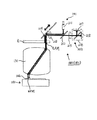
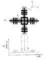
図2は、レチクルアライメント顕微鏡181の概略構成及びレチクルアライメント顕微鏡181を用いたウエハ基準マークWFMとレチクルアライメントマークRAMとの位置合わせ方法を説明するための図である。なお、不図示ではあるが、レチクルアライメント顕微鏡は内焦式の焦点調節機構(AFレンズ)を備えている。
FIG. 2 is a diagram for explaining a schematic configuration of the
図2に示すように、レチクルアライメント顕微鏡181は、検出用照明をレチクルRに導く照明系201、比較的粗い検出を行う(観察倍率が低倍の第1倍率で検出する)図示しないサーチ観察系、及び、比較的精密な検出を行う(観察倍率が高倍の第2倍率で検出する)ファイン観察系203を有する。なお、サーチ観察系は、基本的な構成がファイン観察系203と同じなので図示を省略し、以下の説明においては、ファイン観察系203を中心に説明する。
As shown in FIG. 2, the
照明系201は、検出用照明として露光光(照明ビームIL(図1))を用いる構成となっている。すなわち、照明系201においては、露光光(照明ビームIL)の一部の光束をミラー等で分岐させ、光ファイバ211を用いてレチクルアライメント顕微鏡181内に導いている。レチクルアライメント顕微鏡181に導かれた照明ビームは、ハーフミラー212、第1対物レンズ213及び落射ミラー214を介してレチクルアライメントマークRAMを照明するとともに、レチクルR及び投影光学系130を介して基準板146上のウエハ基準マークWFMを照明する。
The
レチクルアライメントマークRAM及びウエハ基準マークWFMからの反射ビームは、落射ミラー214で各々反射され、レチクルアライメント顕微鏡180の図示しないサーチ観察系及びファイン観察系203に入射する。
Reflected beams from the reticle alignment mark RAM and the wafer reference mark WFM are respectively reflected by the epi-
なお、照明系201は、図示しないが、集光レンズ、結像レンズ、偏向フィルタ及び照明ビームのオン/オフ機構等を有する。照明ビームのオン/オフ機構は、例えば主制御装置160により制御される可動ミラー等で構成され、その反射面の方向を変えることにより、光ファイバ211を介して入射される照明ビームILをアライメント用の照明光として投影光学系130方向に入射させるか否かを制御する。
Although not shown, the
サーチ観察系及びファイン観察系203について、図示しているファイン観察系203を中心に説明する。
The search observation system and the
ファイン観察系203(サーチ観察系)に入射された反射ビームは、第1対物レンズ213、ハーフミラー212、及び、第2対物レンズ215等の光学素子を含むファイン光学系を介して、ファイン観察用カメラ216に入射され、ファイン観察用カメラ216において、レチクルアライメントマークRAM及びウエハ基準マークWFMの重なり合った画像が撮像される。
The reflected beam incident on the fine observation system 203 (search observation system) is used for fine observation via a fine optical system including optical elements such as the first
本実施形態において、ファイン観察用カメラ216は各計測方向(X,Y)ごとにそれぞれCCD等の一次元の撮像素子を用いる。
In the present embodiment, the
図示しないサーチ観察系の構成も、上述したファイン観察系203の構成とほぼ同じである。但し、本実施形態においては、ファイン観察用カメラ216は、これに対応するサーチ観察系のサーチ観察用カメラよりも高感度のものを用いる。また、ファイン光学系は、これに対応するサーチ観察系のサーチ光学系よりも拡大倍率が高く、また、開口数(N.A.)も大きくなるように設定されている。
The configuration of the search observation system (not shown) is almost the same as the configuration of the
なお、これらサーチ観察系及びファイン観察系203には、落射ミラー214及び第1の対物レンズ213を介して入射された反射ビームが、図示しないハーフミラー等で分光されて各々入射される。
Note that the reflected beam incident through the epi-
図示しないサーチ観察用カメラ及び及びファイン観察用カメラ216で撮像された撮像信号(光電変換信号)は、主制御装置160に入力される。
Imaging signals (photoelectric conversion signals) captured by a search observation camera and a fine observation camera 216 (not shown) are input to the
次に、露光装置100におけるレチクルアライメントの基本的な動作について説明する。
Next, a basic operation of reticle alignment in the
露光装置100において、レチクルRの位置決め(アライメント)を行う際には、落射ミラー214がレチクルアライメント顕微鏡181の光路内に挿入され、主制御装置160によりレチクルアライメント顕微鏡181の照明系201の照明ビームのオン/オフ機構が制御されて、光ファイバ211を介して入射される照明ビームILがアライメント用の照明ビームとして用いられ、落射ミラー214を介してレチクルRのレチクルアライメントマークRAM、及び、ウエハステージ142の基準板146に形成されたウエハ基準マークWFMを照明する。
When aligning the reticle R in the
レチクルR及び基準板146での反射ビームは、サーチ観察系のサーチ観察用カメラに入射され、レチクルアライメントマークRAM及びウエハ基準マークWFMの像が、同時に、サーチ観察用カメラの受光面に結像される。また、レチクルR及び基準板146での反射ビームは、ファイン観察系203のファイン観察用カメラ216に入射され、レチクルアライメントマークRAM及びウエハ基準マークWFMの像が、同時に、ファイン観察用カメラ216の受光面に結像される。
The reflected beam from the reticle R and the
ここで、レチクルアライメントマークRAM及びウエハ基準マークWFM、及び、これらを同時に観察した場合の像について、図3〜図5を参照し具体例を挙げて説明する。 Here, the reticle alignment mark RAM, the wafer reference mark WFM, and an image obtained by observing these simultaneously will be described with reference to FIGS.
図3は、レチクルアライメントマークRAMの例を示す図であり、図4は、ウエハ基準マークWFMの例を示す図である。 FIG. 3 is a diagram showing an example of reticle alignment mark RAM, and FIG. 4 is a diagram showing an example of wafer reference mark WFM.
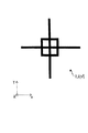
レチクルアライメントマークRAMは、レチクルRの下方に配される面におけるパターン領域の外側に形成されており、例えばパターンジェネレータやEB路光装置といった装置により、設計データに基づいてレチクルRの母材であるガラス板上に転写され、クロムからなる遮光部として所定の形状に形成されている。図3に示す例においては、レチクルアライメントマークRAMは、十字状のマーク要素と矩形状のマーク要素とを組み合わせた構成である。なお、このレチクルアライメントマークRAMと同形状のマークは、レチクルステージ120上に固設された不図示のレチクル基準板上にも、レチクル基準マークとして形成されている。
The reticle alignment mark RAM is formed outside the pattern region on the surface arranged below the reticle R, and is a base material of the reticle R based on design data by a device such as a pattern generator or an EB path light device. It is transferred onto a glass plate and formed in a predetermined shape as a light shielding portion made of chromium. In the example shown in FIG. 3, the reticle alignment mark RAM has a combination of a cross-shaped mark element and a rectangular mark element. A mark having the same shape as the reticle alignment mark RAM is also formed as a reticle reference mark on a reticle reference plate (not shown) fixed on the
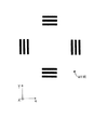
ウエハ基準マークWFMは、ガラスで形成された下地領域上にクロムでマーク要素が形成されている。図4に示す例では、ウエハ基準マークWFMは、Y軸方向に延びた直線状のラインパターンがX軸方向に周期的に配列されたマーク要素と、X軸方向に延びた直線状のラインパターンがY軸方向に周期的に配列されたマーク要素とを組み合わせた構成である。 The wafer reference mark WFM has a mark element made of chrome on a base region made of glass. In the example shown in FIG. 4, the wafer reference mark WFM includes a mark element in which linear line patterns extending in the Y-axis direction are periodically arranged in the X-axis direction, and a linear line pattern extending in the X-axis direction. Is a combination of mark elements periodically arranged in the Y-axis direction.
なお、ウエハ基準マークWFMとして、クロムで形成された下地領域上にガラスでマーク要素を形成してもよい。また、本実施形態では、基準板146をウエハステージ142上に設けているが、基準板146は、定盤141上であれば、例えばウエハホルダー143上や移動ミラー144上等の任意の位置に設けてよい。
As the wafer reference mark WFM, a mark element may be formed of glass on a base region formed of chrome. In this embodiment, the
これらのレチクルアライメントマークRAM及びウエハ基準マークWFMの像が、図示しないサーチ観察用カメラ及びファイン観察用カメラ216の受光面に同時に結像された際の像の例を、図5に示す。 FIG. 5 shows an example of images when these reticle alignment mark RAM and wafer reference mark WFM images are simultaneously formed on the light receiving surfaces of a search observation camera and a fine observation camera 216 (not shown).
図5は、レチクルアライメントマークRAMの中心とウエハ基準マークWFMの中心が一致しており、レチクルRとウエハステージ142との位置合わせが適切に行われた場合の像の例である。レチクルRとウエハステージ142との位置がずれるに連れて、サーチ観察用カメラ及びファイン観察用カメラ216の受光面に結像される像は、レチクルアライメントマークRAMの像の中心とウエハ基準マークWFMの像の中心が、そのずれに応じた方向及び量でずれた像となり、バランスの悪い像となる。
FIG. 5 is an example of an image when the center of the reticle alignment mark RAM and the center of the wafer reference mark WFM coincide with each other and the alignment between the reticle R and the
レチクルアライメントマークRAM及びウエハ基準マークWFMの具体的な形状は、図3及び図4に示す例には限定されないが、例示したように、2次元方向に位置ずれ量を検出することができるような2次元マークであることが望ましい。 The specific shapes of the reticle alignment mark RAM and the wafer reference mark WFM are not limited to the examples shown in FIGS. 3 and 4, but as illustrated, the amount of displacement can be detected in the two-dimensional direction. A two-dimensional mark is desirable.
サーチ観察用カメラ及びファイン観察用カメラ216の各受光面に、このようなレチクルアライメントマークRAM及びウエハ基準マークWFMの重なった像が結像されると、各カメラは、この像の信号をXY各方向に光電変換して光電変換信号(信号波形データ)を生成し、撮像信号として主制御装置160に供給する。
When such an image in which the reticle alignment mark RAM and the wafer reference mark WFM overlap each other is formed on the light receiving surfaces of the search observation camera and the
なお、ファイン観察用カメラ216は、図2に示すように、X軸用のカメラ(センサ)217及びY軸用のカメラ(センサ)218を別個に具備している。X軸用カメラ(一次元ラインCCD)217は、図5(A)に示す予め規定された撮像領域Px内の像を撮像し、これをY方向に光電変換信号を検出することにより、X方向の信号波形データを生成する。また、Y軸用カメラ(一次元ラインCCD)218は、図5(A)に示す予め規定された撮像領域Py内の像を撮像し、これをX方向に光電変換信号を検出することにより、Y方向の信号波形データを生成する。
The
なお、本実施形態では、上述したように、レチクルアライメントマークRAM及びウエハ基準マークWFMの各マーク要素がクロムで形成されていることから、例えばカメラ217の信号は図5(B)に示すように、そのマーク要素で反射したビームの強度が強く、そのマーク要素に対応する部分で信号強度が強くなっているような信号波形データが生成される。
In this embodiment, as described above, since the mark elements of the reticle alignment mark RAM and the wafer reference mark WFM are formed of chrome, for example, the signal of the
主制御装置160は、入力される信号波形データに基づいて、所定のアルゴリズムに従って、レチクルアライメントマークRAM及びウエハ基準マークWFMとの相対的な位置関係を算出する。そして、その算出結果に基づいて、レチクルRの位置及び姿勢を調整する。
なお、このレチクルアライメントでは、まず、サーチ観察系の観察結果に基づいて、比較的粗くレチクルアライメントマークRAMを位置決めした後に、ファイン観察系203の観察結果に基づいて、精密なレチクルRの位置決めを行う。
In this reticle alignment, first, the reticle alignment mark RAM is positioned relatively coarsely based on the observation result of the search observation system, and then the precise reticle R is positioned based on the observation result of the
次に、本発明にレチクルレチクルアライメントに伴うマークの位置計測動作について説明する。 Next, the mark position measurement operation associated with reticle reticle alignment in the present invention will be described.
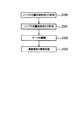
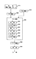
図6は、レチクルアライメントに伴うマークの位置計測動作、特に、上述したファイン観察系203を用いたレチクルの位置決め処理(ファインアライメント処理)に伴うマークの位置計測動作の手順を示すフローチャートである。
FIG. 6 is a flowchart showing the procedure of mark position measurement operation associated with reticle alignment, in particular, the mark position measurement operation associated with reticle positioning processing (fine alignment processing) using the
本実施形態の位置計測動作では、マークを実際に撮像した信号を信号処理する前に、その信号に含まれるノイズを予め計測し、その計測結果を信号処理に用いる。以下、ファインアライメント処理に伴うマークの位置計測動作について、図6を参照して説明する。 In the position measurement operation of this embodiment, before performing signal processing on a signal obtained by actually imaging a mark, noise included in the signal is measured in advance, and the measurement result is used for signal processing. Hereinafter, the mark position measurement operation associated with the fine alignment process will be described with reference to FIG.
まず、主制御装置160は、レチクルアライメント顕微鏡181及び182の撮像信号に含まれるノイズの光量非依存成分を計測する(ステップS100)。レチクルアライメント顕微鏡181について代表して説明する。主制御装置160は、レチクルアライメント顕微鏡181の照明系201の照明ビームのオン/オフ機構を制御して、光ファイバ211を介して入射される照明ビームILがアライメント用の照明ビームとして用いられないようにし、この状態でファイン観察用カメラ216の信号を取得する。照明ビームがレチクルアライメント顕微鏡181のファイン観察用カメラ216に観察されない状態でファイン観察用カメラ216の信号を取得することにより、ノイズの光量非依存成分の計測を行うことができる。このノイズ成分は、ファイン観察用カメラ216の暗電流成分である。主制御装置160は、計測したノイズの光量非依存成分の情報を記憶する。
First,
次に、主制御装置160は、レチクルアライメント顕微鏡181及び182の撮像信号に含まれるノイズの光量依存成分を計測する(ステップS101)。ノイズの光量依存成分は、レチクルR及び基準板146上でそれぞれレチクルアライメントマークRAM及びウエハ基準マークWFMが形成されたマーク領域とは異なる非マーク領域(マークの存在しない領域:下地領域)を照明ビームで照明し、この非マーク領域(下地領域、又は無地領域)を、レチクルアライメント顕微鏡181及び182を介して撮像することにより行う。その際、本発明に係る方法においては、その非マーク領域の表面について、光学系の条件により決定される最適結像条件(ベストフォーカス状態)に対して十分にデフォーカスした状態となるように、その光学系の条件を設定する。
Next,
具体的に説明すると、ノイズの光量依存成分を計測する場合、主制御装置160は、予め定められた設計値に基づいて、例えば基準板146のウエハ基準マークWFMが形成されていない非マーク領域がレチクルアライメント顕微鏡181の観察位置に配置されるように、駆動系147を介してウエハステージ142をXY2次元方向に移動させる。次に、主制御装置160は、レチクルアライメント顕微鏡181内の前述(不図示)の内焦式の焦点調節機構を用いて、レチクル又はレチクル基準板のパターン形成面上に対してレチクルアライメント系181をフォーカスさせる(レチクルパターン面とレチクルアライメント系のベストフォーカス位置とを一致させる)。次に、主制御装置160は、基準板146の表面のZ方向の位置が、投影光学系130を介して検出するレチクルアライメント系のベストフォーカス位置から十分にずれるように(デフォーカスするように)、駆動系147を介してウエハステージ142をZ方向に移動させる。例えば、図7に示すように、ウエハステージ142の位置を(投影光学系の)ベストフォーカス位置から約30μm下げる。(これにより、レチクルパターン面と基準板146との共役関係はくずされる。)そして、この状態で、基準板146の非マーク領域を観察する。その結果、基準板146等の表面に付着したゴミや欠陥は、この時撮像されない。仮に撮像されたとしても、十分に低周波な成分となり、マークパターンから得られた適正な信号波形データに対する影響は少なくなる。なお、観察した光量依存成分の計測値は、主制御装置160に記憶される。
More specifically, when measuring the light quantity-dependent component of noise, the
非マーク領域は、レチクルアライメントマークRAM及びウエハ基準マークWFMの各マークパターンが形成された下地領域と同じ材質からなる。従って、この非マーク領域からの反射ビームを観察した信号を取得することにより、レチクルアライメント顕微鏡181及び182におけるノイズの光量依存成分を計測することができる。
The non-mark area is made of the same material as the base area on which the mark patterns of the reticle alignment mark RAM and the wafer reference mark WFM are formed. Therefore, by acquiring a signal obtained by observing the reflected beam from the non-marked region, it is possible to measure the light quantity dependent component of noise in the
なお、このノイズ成分は、レチクルアライメント顕微鏡181及び182を照明ビームが通過することにより生じるものであり、その原因は、ファイン観察用カメラ216(X軸用カメラ217及びY軸用カメラ218)のカバーガラスやハーフミラー等の光学系の干渉縞や、あるいはファイン観察用カメラ216の画素間の感度ばらつき等がある。こうしたノイズは、レチクルアライメント顕微鏡181及び182を通過する照明ビームの光量に対してほぼ比例的に変化し、照明ビームの光量が大きいほど大きく生じる傾向にある。
This noise component is generated when the illumination beam passes through the
これらの光量非依存成分及び光量依存成分を計測するタイミングは、マークの撮像信号を信号処理する前であれば任意のタイミングで実施可能である。例えば、所定の期間ごとに実施してもよいし、装置の立ち上げごとに実施してもよい。あるいは、ノイズに影響を及ぼす温度、気圧等の環境因子を計測し、その計測結果に基づいてノイズの計測タイミングを決定してもよい。 The timing for measuring the light amount-independent component and the light amount-dependent component can be implemented at an arbitrary timing as long as it is before signal processing of the mark imaging signal. For example, it may be performed every predetermined period or every time the apparatus is started up. Alternatively, environmental factors such as temperature and atmospheric pressure that affect noise may be measured, and noise measurement timing may be determined based on the measurement results.
次に、主制御装置160は、実際にマークを観察し、その撮像信号を得る(ステップS102)。すなわち、主制御装置160は、予め定められた設計値に基づいて、基準板146上のウエハ基準マークWFMの中心点が投影光学系130の光軸AX上に位置するように、レーザ干渉計145の出力をモニタしつつ、ウエハステージ142を移動させる。続いて、主制御装置160は、レチクルアライメント顕微鏡181及び182を用いて、照明ビームをレチクルRに導くとともに、レチクルR上のレチクルアライメントマークRAM及び基準板146上のウエハ基準マークWFMを同時に観察する。
Next,
次に、主制御装置160は、レチクルアライメントマークRAM及びウエハ基準マークWFMを同時に観察した結果と、上述したノイズの計測結果(ステップS100とステップS101の計測結果)とに基づいて、所定のアルゴリズムで信号処理を行い、レチクルアライメントマークRAM及びウエハ基準マークWFMの相対的な位置関係を計測する(ステップS103)。
Next,
以上説明した一連の位置計測動作により、撮像信号にノイズが含まれる場合においても、そのノイズの影響が補正され、レチクルアライメントマークRAMとウエハ基準マークWFMとの相対的な位置関係を精度よく計測することができる。 By the series of position measurement operations described above, even when the imaging signal includes noise, the influence of the noise is corrected, and the relative positional relationship between the reticle alignment mark RAM and the wafer reference mark WFM is accurately measured. be able to.
なお、このようにして計測されたレチクルアライメントマークRAMとウエハ基準マークWFMの相対的な位置関係は、例えばレチクルRの初期設定としての投影光学系130に対する位置決め、すなわちレチクルアライメントに使用される。
Note that the relative positional relationship between the reticle alignment mark RAM and the wafer reference mark WFM thus measured is used, for example, for positioning the reticle R with respect to the projection
また、この相対位置計測と同時に、ウエハアライメントセンサ170を用いて基準板146上の他の基準マークを観察することにより、ウエハアライメントセンサ170の指標との相対位置関係が計測され、いわゆるベースライン量が算出される。
Simultaneously with this relative position measurement, by observing another reference mark on the
また、このようなレチクルアライメント及びベースライン計測の後、主制御装置160は、ウエハW上の複数ショット領域に設けられたウエハアライメントマークの位置を、ウエハアライメントセンサ170を用いて順次計測し、いわゆるEGA(エンハンスト・グローバル・アライメント)の手法により、ウエハW上の全てのショット配列データを求める。そして、この配列データに従って、ウエハW上のショット領域を順次投影光学系130の真下の露光位置に移動させ、光源111を制御し、いわゆるステップ・アンド・リピート方式で順次露光を行う。
Further, after such reticle alignment and baseline measurement,
次に、実際のマークに対する信号波形データを具体的に示す。 Next, signal waveform data for an actual mark is specifically shown.
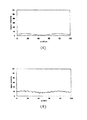
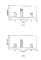
まず、ステップS100によりノイズの光量非依存成分を計測することにより、例えば図8(A)に示すような光量非依存成分の信号波形データが得られる。 First, by measuring the noise light amount-independent component in step S100, signal waveform data of the light amount-independent component as shown in FIG. 8A, for example, is obtained.
次に、ステップS101によりノイズの光量依存成分を計測することにより、例えば図8(B)に示すような光量依存成分の信号波形データが得られる。 Next, by measuring the light quantity dependent component of noise in step S101, signal waveform data of the light quantity dependent component as shown in FIG. 8B, for example, is obtained.
次に、ステップS102においてレチクルアライメントマークRAM及びウエハ基準マークWFMをファイン観察用カメラ216で撮像した結果、例えばそのX方向の信号波形データとして、図9(A)に示す信号が得られる。
Next, as a result of imaging the reticle alignment mark RAM and the wafer reference mark WFM with the
得られた図9(A)に示す信号に対して、図8(A)に示したノイズの光量非依存成分の情報、及び、図8(B)に示すノイズの光量依存成分の情報に基づいて、次式(1)により補正を行うことにより、図9(B)に示すような信号波形データが得られる。 The obtained signal shown in FIG. 9A is based on the information on the light quantity independent component of noise shown in FIG. 8A and the information on the light quantity dependent component of noise shown in FIG. Thus, signal waveform data as shown in FIG. 9B is obtained by performing correction according to the following equation (1).
但し、式(1)において、Dは補正後のマーク信号波形データ、Dmは補正前の観測されたマーク信号波形データ、Dnaはノイズの光量依存成分の信号波形データ、及び、Dnbはノイズの光量非依存成分の信号波形データである。 In equation (1), D is the mark signal waveform data after correction, Dm is the observed mark signal waveform data before correction, Dna is the signal waveform data of the noise light quantity dependent component, and Dnb is the noise light quantity. This is signal waveform data of an independent component.
D=(Dm−Dnb)/(Dna−Dnb) …(1)
このアルゴリズムでは、ノイズ補正前のマーク信号波形データDmからノイズの光量非依存成分Dnbを減算した結果に対して、ノイズの光量依存成分からノイズの光量非依存成分Dnbを減じた結果で除算処理している。そしてその結果、図9(B)より明らかな通り、マーク信号波形データに対するノイズの影響が適切に補正されている。
D = (Dm−Dnb) / (Dna−Dnb) (1)
In this algorithm, the result of subtracting the noise light amount independent component Dnb from the mark signal waveform data Dm before noise correction is divided by the result of subtracting the noise light amount independent component Dnb from the noise light amount dependent component. ing. As a result, as apparent from FIG. 9B, the influence of noise on the mark signal waveform data is appropriately corrected.
このように、本発明の第1実施形態によれば、基準板146の非マーク領域にデフォーカス状態で照明ビームを照射し、その反射光から光量依存成分の下地波形を検出することにより、基準板146の表面のゴミや欠陥がノイズとして下地波形に現れることを回避している。従って、ゴミや欠陥の影響を受けない適切な光量依存成分を有する下地波形を検出することができ、下地補正を適切に行うことができ、高精度にレチクルのパターンとウエハ(及びウエハ上の既存のパターン)とを位置合わせすることができる。その結果、高精細で高性能な電子デバイスを製造することができる。
As described above, according to the first embodiment of the present invention, the
第2実施形態
本発明の第2実施形態について、図10を参照して説明する。
Second Embodiment A second embodiment of the present invention will be described with reference to FIG.
第2実施形態においては、レチクルアライメントの下地補正を行う際に使用する光量依存成分を検出する方法が第1実施形態と異なり、露光装置100の構成、レチクルアライメントの方法、そのための位置計測処理の流れ等は、何れも上述した第1実施形態と同じである。
Unlike the first embodiment, the second embodiment differs from the first embodiment in a method of detecting a light amount-dependent component used when performing base correction for reticle alignment. The configuration of the
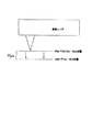
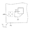
本実施形態においては、下地波形の光量依存成分を検出する際に、基準板146を移動させながらその表面の非マーク領域を撮像する。具体的には、図10に示すように、レチクルアライメント顕微鏡181からの照明ビームを、基準板146の非マーク領域301に照射する。この時、フォーカスは基準板146の表面に合っていてよい。
In this embodiment, when detecting the light amount-dependent component of the background waveform, the non-mark area on the surface is imaged while moving the
この状態で、主制御装置160が駆動系147を制御して、基準板146を水平方向の任意の方向に移動させる。図10に示す例においては、基準板146はXY軸と各々45度をなす方向で紙面左下方向に移動する。その結果、照明ビームの照射領域(非マーク領域/下地領域)301は、図示のごとく、相対的に基準板146上を右上方向に移動する。この間の所定時間の反射ビームをレチクルアライメント顕微鏡181のファイン観察系203で検出し、その撮像信号から下地波形を検出する。
In this state,
このような動作をすると、例えば基準板146の照明領域にゴミ302が存在していた場合、このゴミ302の信号は、レチクルアライメント顕微鏡181のファイン観察用カメラ216により明確に観察される。しかしながら、基準板146が移動することによりゴミ302の位置もファイン観察用カメラ216の視野内を移動する。しかも、その移動方向はXY軸と各々45度をなす方向なので、ゴミ302に起因する信号変形分は、XY方向の各位置に対して連続的に観察されることとなる。従って、ゴミ302の信号は、観察される下地波形において、直流成分、あるいは、非常に低周波の信号成分として観察されることとなり、実質的にノイズと言われるようなパターン波形と類似した高周波な信号ではなくなる。
With this operation, for example, when
従って、これに起因していわゆるだまされが発生するような状況は回避することができる。 Therefore, it is possible to avoid a situation in which so-called fooling occurs due to this.
このように、本発明の第2実施形態によれば、基準板146を移動させながら非マーク領域に照明ビームを照射し、その反射光から光量依存成分の下地波形(下地信号)を検出することにより、基準板146の表面のゴミや欠陥が高周波のノイズとして下地波形に現れることを回避した。従って、ゴミや欠陥の影響を受けない適切な光量依存成分を有する下地波形を検出することができ、下地補正を適切に行うことができ、高精度にレチクルのパターンとウエハ(及びウエハ上の既存のパターン)とを位置合わせすることができる。その結果、高精細で高性能な電子デバイスを製造することができる。
As described above, according to the second embodiment of the present invention, the illumination beam is irradiated to the non-mark area while moving the
なお、基準板146の移動方向は、任意の方向でよいが、ゴミや欠陥の成分が、XY各軸方向に平均化した状態で均一に現れるようにするためには、本実施形態のように、XY各軸に対して交差する方向(特に好ましくは45度をなす方向)に移動させるのが好適である。
The moving direction of the
第3実施形態
本発明の第3実施形態について、図11を参照して説明する。
Third Embodiment A third embodiment of the present invention will be described with reference to FIG.
第3実施形態においても、レチクルアライメントの下地補正を行う際に使用する光量依存成分を検出する方法が、第1実施形態及び第2実施形態と異なる。その他の露光装置100の構成、レチクルアライメントの方法、そのための位置計測処理の流れ等は、何れも上述した第1実施形態と同じである。
Also in the third embodiment, a method for detecting a light amount-dependent component used when performing reticle alignment background correction is different from the first embodiment and the second embodiment. The other configurations of the
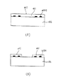
本実施形態においては、図11(A)に示すように、基準板146の表面に透明な層401を積層し、このような基準板146を用いて下地波形の光量依存成分を検出する。すなわち、基準板146の表面の非マーク領域に対して、透明層401を介して照明ビームを照射し、その反射光を撮像して下地波形を検出する。照明ビームのフォーカスは、ウエハ基準マークWFMが形成されている基準板146と透明層401との接合面に対して合わせればよい。なお、本実施形態において、透明層401は石英や蛍石等を素材として形成し、その透明層401の厚さは、約100μmである。
In the present embodiment, as shown in FIG. 11A, a
このような構成とすれば、ゴミや欠陥が発生する場合、これは、透明層401の表面(透明層401と周囲雰囲気との境界表面)に発生する可能性が非常に高い。光量依存成分を検出するための光ビームは、基準板146と透明層401との間の接合面にフォーカスが合わされているので、透明層401の表面はデフォーカスされた状態である。従って、この面にゴミや欠陥が生じたとしても、第1実施形態の場合と同様に、これが下地波形(下地信号)に現れることはない。
With such a configuration, when dust or a defect is generated, it is very likely that this will occur on the surface of the transparent layer 401 (the boundary surface between the
従って、これに起因していわゆるだまされが発生するような状況は回避することができる。 Therefore, it is possible to avoid a situation in which so-called fooling occurs due to this.
このように、第3実施形態によれば、基準板146の表面に透明層401を形成することにより、ゴミや欠陥が発生する表面を実質的にデフォーカスした位置に移動させている。従って、通常通りに基準板146の表面の非マーク領域に照明ビームを照射し、その反射光から光量依存成分の下地波形を検出することにより、ゴミや欠陥の影響を受けない適切な光量依存成分を有する下地波形を検出することができ、下地補正を適切に行うことができ、高精度にレチクルのパターンとウエハ(及びウエハ上の既存のパターン)とを位置合わせすることができる。その結果、高精細で高性能な電子デバイスを製造することができる。
As described above, according to the third embodiment, by forming the
なお、基準板146上に形成する透明層401は、図11(B)に示すように、下地波形を検出するための照明ビームを照射する領域にのみ部分的に形成するようにしてもよい。
Note that the
変形例
本実施の形態は、本発明の理解を容易にするために記載されたものであって本発明を何ら限定するものではない。本実施の形態に開示された各要素は、本発明の技術的範囲に属する全ての設計変更や均等物をも含み、また任意好適な種々の改変が可能である。
Modifications This embodiment has been described in order to facilitate understanding of the present invention, and does not limit the present invention. Each element disclosed in the present embodiment includes all design changes and equivalents belonging to the technical scope of the present invention, and various suitable modifications are possible.
例えば、光量依存成分の下地波形を検出する際に、レチクルや、レチクルステージ上に搭載されているレチクル基板板のパターン面上におけるクロム(Cr)部分(パターンが形成されていない領域)を用いて計測をするようにしてもよい。レチクル又はRFM上にゴミや欠陥が発生しても、ガラス基板の厚み分デフォーカスされるため、ゴミや欠陥が像を結ぶことは回避でき、第1実施形態あるいは第3実施形態と同様に、適正な光量依存成分を検出することができる。なお、この場合においてウエハステージ側は、どのようなパターンが下地としてこようと構わない(なぜなら、レチクル又はレチクル基準板のクロム部材により透明光は透過されずに全反射されるため)。しかしながら、レチクルとしてハーフトーンレチクルを用いる場合には、ウエハステージ側の下地としては、パターンの無い領域を配置しておくことが望ましい。 For example, when detecting a ground waveform of a light amount dependent component, a chrome (Cr) portion (a region where a pattern is not formed) on a reticle or a pattern surface of a reticle substrate plate mounted on a reticle stage is used. You may make it measure. Even if dust or a defect occurs on the reticle or RFM, defocusing is performed by the thickness of the glass substrate, so that it is possible to avoid the dust and the defect from forming an image. As in the first embodiment or the third embodiment, An appropriate light quantity dependent component can be detected. In this case, any pattern may be used as the base on the wafer stage side (because the transparent light is not transmitted by the chrome member of the reticle or reticle reference plate but totally reflected). However, when a halftone reticle is used as the reticle, it is desirable to arrange an area without a pattern as the base on the wafer stage side.
また、露光システムの全体構成は、図1に示した構成に限られるものではない。 Further, the overall configuration of the exposure system is not limited to the configuration shown in FIG.
また、本発明はステップ・アンド・スキャン方式の露光装置に限らず、ステップ・アンド・リピート方式、又はプロキシミティ方式の露光装置(X線露光装置等)や、液浸露光装置等、各種方式の露光装置にも適用が可能である。 The present invention is not limited to a step-and-scan type exposure apparatus, but can be applied to various types such as a step-and-repeat type or proximity-type exposure apparatus (such as an X-ray exposure apparatus) and an immersion exposure apparatus. The present invention can also be applied to an exposure apparatus.
また、露光装置で用いる露光用照明光(エネルギビーム)は紫外光に限られるものではなく、X線(EUV光を含む)、電子線やイオンビーム等の荷電粒子線等でもよい。また、DNAチップ、マスク又はレチクル等の製造用に用いられる露光装置でもよい。 The exposure illumination light (energy beam) used in the exposure apparatus is not limited to ultraviolet light, and may be charged particle beams such as X-rays (including EUV light), electron beams and ion beams. Moreover, the exposure apparatus used for manufacture of a DNA chip, a mask or a reticle may be used.
デバイス製造工程
次に、上述した露光装置100をリソグラフィー工程において使用したデバイスの製造方法について図12を参照して説明する。
Device Manufacturing Process Next, a device manufacturing method using the
図12は、例えばICやLSI等の半導体チップ、液晶パネル、CCD、薄膜磁気ヘッド、マイクロマシン等の電子デバイスの製造工程を示すフローチャートである。 FIG. 12 is a flowchart showing a manufacturing process of an electronic device such as a semiconductor chip such as an IC or LSI, a liquid crystal panel, a CCD, a thin film magnetic head, or a micromachine.
図12に示すように、電子デバイスの製造工程においては、まず、電子デバイスの回路設計等のデバイスの機能・性能設計を行い、その機能を実現するためのパターン設計を行い(工程S810)、次に、設計した回路パターンを形成したレチクルを製作する(工程S820)。 As shown in FIG. 12, in the manufacturing process of the electronic device, first, the function / performance design of the device such as the circuit design of the electronic device is performed, and the pattern design for realizing the function is performed (step S810). Then, a reticle on which the designed circuit pattern is formed is manufactured (step S820).
一方、シリコン等の材料を用いてウエハ(シリコン基板)を製造する(工程S830)。 On the other hand, a wafer (silicon substrate) is manufactured using a material such as silicon (step S830).
次に、工程S820で製作したレチクル及び工程S830で製造したウエハを使用して、リソグラフィー技術等によってウエハ上に実際の回路等を形成する(工程S840)。 Next, using the reticle manufactured in step S820 and the wafer manufactured in step S830, an actual circuit or the like is formed on the wafer by a lithography technique or the like (step S840).
具体的には、まず、ウエハ表面に、絶縁膜、電極配線膜あるいは半導体膜との薄膜を成膜し(工程S841)、次に、この薄膜の全面にレジスト塗布装置(コータ)を用いて感光剤(レジスト)を塗布する(工程S842)。 Specifically, first, a thin film with an insulating film, an electrode wiring film, or a semiconductor film is formed on the wafer surface (step S841), and then the entire surface of the thin film is exposed using a resist coating apparatus (coater). An agent (resist) is applied (step S842).
次に、このレジスト塗布後の基板をウエハホルダー上にロードするとともに、工程S830において製造したレチクルをレチクルステージ上にロードして、そのレチクルに形成されたパターンをウエハ上に縮小転写する(工程S843)。この時、露光装置においては、上述した本発明に係る位置合わせ方法によりウエハの各ショット領域を順次位置合わせし、各ショット領域にレチクルのパターンを順次転写する。 Next, the resist-coated substrate is loaded onto the wafer holder, and the reticle manufactured in step S830 is loaded onto the reticle stage, and the pattern formed on the reticle is reduced and transferred onto the wafer (step S843). ). At this time, the exposure apparatus sequentially aligns each shot area of the wafer by the above-described alignment method according to the present invention, and sequentially transfers the reticle pattern to each shot area.
露光が終了したら、ウエハをウエハホルダーからアンロードし、現像装置(デベロッパ)を用いて現像する(工程S844)。これにより、ウエハ表面にレチクルパターンのレジスト像が形成される。 When the exposure is completed, the wafer is unloaded from the wafer holder and developed using a developing device (developer) (step S844). Thereby, a resist image of a reticle pattern is formed on the wafer surface.
そして、現像処理が終了したウエハに、エッチング装置を用いてエッチング処理を施し(工程S845)、ウエハ表面に残存するレジストを、例えばプラズマアッシング装置等を用いて除去する(工程S846)。 Then, the wafer subjected to the development process is etched using an etching apparatus (step S845), and the resist remaining on the wafer surface is removed using, for example, a plasma ashing apparatus (step S846).
これにより、ウエハの各ショット領域に、絶縁層や電極配線等のパターンが形成される。そして、この処理をレチクルを変えて順次繰り返すことにより、ウエハ上に実際の回路等が形成される。 Thereby, patterns such as an insulating layer and electrode wiring are formed in each shot region of the wafer. Then, by repeating this process sequentially with the reticle changed, an actual circuit or the like is formed on the wafer.
ウエハ上に回路等が形成されたら、次に、デバイスとしての組み立てを行う(工程S850)。具体的には、ウエハをダイシングして個々のチップに分割し、各チップをリードフレームやパッケージに装着し電極を接続するボンディングを行い、樹脂封止等パッケージング処理を行う。 If a circuit or the like is formed on the wafer, then assembling as a device is performed (step S850). Specifically, the wafer is diced and divided into individual chips, each chip is mounted on a lead frame or a package, bonding for connecting electrodes is performed, and a packaging process such as resin sealing is performed.
そして、製造したデバイスの動作確認テスト、耐久性テスト等の検査を行い(工程S860)、デバイス完成品として出荷する。 Then, inspections such as an operation confirmation test and a durability test of the manufactured device are performed (step S860), and the device is shipped as a finished device.
100…露光装置
110…照明系
111…光源
112…照度均一化光学系
113…照明系開口絞り板
114…レボルバ駆動系
116…リレー光学系
117…折り曲げミラー
120…レチクルステージ
130…投影光学系
140…ウエハステージ部
141…定盤
142…ウエハステージ
143…ウエハホルダー
144…移動ミラー
145…レーザ干渉計
146…基準板
147…駆動系
150…メインフォーカス系
151…照射光学系
152…受光光学系
160…主制御装置
170…ウエハアライメントセンサ
180…レチクルアライメント顕微鏡部
181,182…レチクルアライメント顕微鏡
201…照明系
203…ファイン観察系
211…光ファイバ
212…ハーフミラー
213…第1の対物レンズ
214…落射ミラー
215…第2の対物レンズ
216…ファイン観察用カメラ
217…X軸用カメラ
218…Y軸用カメラ
301…照明領域(非マーク領域)
302,402…ゴミ
401…透明層
DESCRIPTION OF
201 ... Lighting system
203 ... Fine observation system
211 ... Optical fiber
212 ... Half mirror
213: First objective lens
214 ... Falling mirror
215: Second objective lens
216 ... Fine observation camera
217 ... Camera for X axis
218 ... Y-
302, 402 ...
Claims (8)
前記マークが形成されている前記物体上のパターン形成面上であって、且つ該マークの存在しない領域である下地領域を、前記観察系の観察視野内に配置する第1工程と、
前記下地領域上の前記光ビームの入射側に該光ビームを透過する物質層が存在する場合には、前記物質層の前記光ビーム入射側の表面に対して前記観察系がデフォーカスした状態下で前記下地領域を検出し、前記下地領域上に前記物質層が存在しない場合には、該下地領域の表面に対して該観察系がデフォーカスした状態下で該下地領域を検出する第2工程と、
前記第2工程での検出結果に基づいて、前記光量依存成分を検出する第3工程とを有することを特徴とする位置計測方法。 A mark signal obtained by irradiating a mark formed on an object with a light beam, receiving a reflected beam from the mark through an observation system, and receiving the light based on a ground signal including a light quantity dependent component detected in advance. Is a position measurement method for obtaining a correction mark signal and measuring the position of the mark based on the correction mark signal,
A first step of disposing a ground region on the pattern forming surface on the object on which the mark is formed and the region where the mark is not present in an observation field of the observation system;
When there is a material layer that transmits the light beam on the incident side of the light beam on the base region, the observation system is defocused on the surface of the material layer on the light beam incident side. A second step of detecting the base region in a state in which the observation system is defocused with respect to the surface of the base region when the base layer is detected in step S3 and the material layer is not present on the base region When,
And a third step of detecting the light quantity dependent component based on a detection result in the second step.
前記マークが形成されている前記物体上のパターン形成面上であって、且つ該マークの存在しない領域である下地領域を、前記観察系の観察視野内に配置する第1工程と、
前記下地領域に対して前記光ビームを照射した状態で、前記パターン形成面と平行な面に沿って該下地領域と該光ビームとを相対的に移動させながら、前記下地領域からの反射ビームを前記観察系を介して受光する第2工程と、
前記第2工程で受光した信号に基づいて、前記光量依存成分を検出する第3工程とを有することを特徴とする位置計測方法。 A mark signal obtained by irradiating a mark formed on an object with a light beam, receiving a reflected beam from the mark through an observation system, and receiving the light based on a ground signal including a light quantity dependent component detected in advance. Is a position measurement method for obtaining a correction mark signal and measuring the position of the mark based on the correction mark signal,
A first step of disposing a ground region on the pattern forming surface on the object on which the mark is formed and the region where the mark is not present in an observation field of the observation system;
While irradiating the base region with the light beam, the base region and the light beam are relatively moved along a plane parallel to the pattern formation surface, and a reflected beam from the base region is irradiated. A second step of receiving light through the observation system;
And a third step of detecting the light quantity dependent component based on the signal received in the second step.
前記マスク上のパターン形成面上であり且つ前記マスクマーク又はパターンの存在しない領域である第1下地領域、あるいは前記マスクステージ上に固設され第2基準マークを備えた第2基準部材上の基準パターン形成面上の該第2基準マークの存在しない領域である第2下地領域を、前記観察系の観察視野内に配置する第1工程と、
前記第1下地領域又は前記第2下地領域からの反射ビームを前記観察系を介して受光する第2工程と、
前記第2工程で受光した信号に基づいて、前記光量依存成分を検出する第3工程とを有することを特徴とする位置計測方法。 A light beam is applied to the first reference mark formed on the first reference member fixed on the substrate stage on which the substrate is placed and the mask mark formed on the mask placed on the mask stage. Then, a reflected beam from each mark is received through an observation system, and a correction mark signal is obtained by correcting the signal obtained by receiving the received light based on a ground signal including a light quantity dependent component detected in advance. A position measurement method for measuring the position of the mark based on a signal,
A reference on a first reference region on the pattern forming surface on the mask and where the mask mark or pattern does not exist, or on a second reference member provided with a second reference mark fixed on the mask stage A first step of disposing a second base region, which is a region where the second reference mark is not present, on the pattern forming surface within an observation field of view of the observation system;
A second step of receiving a reflected beam from the first base region or the second base region through the observation system;
And a third step of detecting the light quantity dependent component based on the signal received in the second step.
請求項1に記載の位置計測方法を使用するとともに、
前記物体は前記基板を載置する基板ステージ上に固設され、前記マークとしての基準マークが形成される基準パターン面を備えた基準部材であり、
前記デフォーカスした状態とは、前記観察系が前記マスク上のパターン形成面に対してはフォーカスした状態でありながら、前記投影光学系を介した前記物質層の表面、又は前記基準パターン面に対してはデフォーカスした状態であること、を含むことを特徴とする露光方法。 An exposure method for transferring a pattern formed on a mask onto a substrate via a projection optical system,
While using the position measuring method according to claim 1,
The object is a reference member that is fixed on a substrate stage on which the substrate is placed and has a reference pattern surface on which a reference mark as the mark is formed,
The defocused state is a state in which the observation system is focused on the pattern formation surface on the mask, but with respect to the surface of the material layer via the projection optical system or the reference pattern surface. An exposure method characterized by including a defocused state.
前記マスク又は前記基板の少なくとも何れか一方について、請求項1〜4の何れか一項に記載の位置計測方法により位置を計測し、当該計測結果に基づいて前記マスク又は前記基板の位置決めを行うことを特徴とする露光方法。 An exposure method for transferring a pattern formed on a mask onto a substrate,
The position of at least one of the mask and the substrate is measured by the position measurement method according to claim 1, and the mask or the substrate is positioned based on the measurement result. An exposure method characterized by the above.
請求項1〜4の何れか一項に記載の位置計測方法により前記マスク又は前記基板の少なくとも何れか一方の位置を計測する位置計測手段を有することを特徴とする露光装置。 An exposure apparatus for transferring a pattern formed on a mask onto a substrate,
An exposure apparatus, comprising: a position measurement unit that measures the position of at least one of the mask and the substrate by the position measurement method according to claim 1.
Priority Applications (1)
| Application Number | Priority Date | Filing Date | Title |
|---|---|---|---|
| JP2004105914A JP2005294450A (en) | 2004-03-31 | 2004-03-31 | Position measuring method, exposure method and apparatus, and device manufacturing method |
Applications Claiming Priority (1)
| Application Number | Priority Date | Filing Date | Title |
|---|---|---|---|
| JP2004105914A JP2005294450A (en) | 2004-03-31 | 2004-03-31 | Position measuring method, exposure method and apparatus, and device manufacturing method |
Publications (1)
| Publication Number | Publication Date |
|---|---|
| JP2005294450A true JP2005294450A (en) | 2005-10-20 |
Family
ID=35327065
Family Applications (1)
| Application Number | Title | Priority Date | Filing Date |
|---|---|---|---|
| JP2004105914A Pending JP2005294450A (en) | 2004-03-31 | 2004-03-31 | Position measuring method, exposure method and apparatus, and device manufacturing method |
Country Status (1)
| Country | Link |
|---|---|
| JP (1) | JP2005294450A (en) |
Cited By (2)
| Publication number | Priority date | Publication date | Assignee | Title |
|---|---|---|---|---|
| JP2015023145A (en) * | 2013-07-18 | 2015-02-02 | キヤノン株式会社 | Detection device, exposure device and article manufacturing method |
| JP2023085733A (en) * | 2021-12-09 | 2023-06-21 | 浜松ホトニクス株式会社 | Laser processing device |
-
2004
- 2004-03-31 JP JP2004105914A patent/JP2005294450A/en active Pending
Cited By (3)
| Publication number | Priority date | Publication date | Assignee | Title |
|---|---|---|---|---|
| JP2015023145A (en) * | 2013-07-18 | 2015-02-02 | キヤノン株式会社 | Detection device, exposure device and article manufacturing method |
| JP2023085733A (en) * | 2021-12-09 | 2023-06-21 | 浜松ホトニクス株式会社 | Laser processing device |
| JP7682780B2 (en) | 2021-12-09 | 2025-05-26 | 浜松ホトニクス株式会社 | Laser Processing Equipment |
Similar Documents
| Publication | Publication Date | Title |
|---|---|---|
| US7791718B2 (en) | Measurement method, exposure method, and device manufacturing method | |
| JP2002198303A (en) | Exposure apparatus, optical characteristic measuring method, and device manufacturing method | |
| JP2001274080A (en) | Scanning projection exposure apparatus and alignment method thereof | |
| JP2019179186A (en) | Lithography device, pattern forming method and method for manufacturing article | |
| TW473823B (en) | Exposure method as well as exposure apparatus, and method for manufacturing device | |
| TW201101369A (en) | Exposure method and device manufacturing method, and overlay error measuring method | |
| JPH11233434A (en) | Exposure condition determination method, exposure method, exposure apparatus, and device manufacturing method | |
| JPWO2003104746A1 (en) | Position measuring method, exposure method, exposure apparatus, and device manufacturing method | |
| JP2007250947A (en) | Exposure apparatus and image plane detection method | |
| JPH10189443A (en) | Position detecting mark, mark detecting method and apparatus, and exposure apparatus | |
| JP2006030021A (en) | Position detection apparatus and position detection method | |
| US20040027573A1 (en) | Position measuring method, exposure method and system thereof, device production method | |
| JP3441930B2 (en) | Scanning exposure apparatus and device manufacturing method | |
| JP2002170757A (en) | Position measuring method and apparatus, exposure method and apparatus, device manufacturing method | |
| TW527638B (en) | Evaluating method of lithography system, adjusting method for substrate-processing apparatus, lithography system and exposure apparatus | |
| JP2005294450A (en) | Position measuring method, exposure method and apparatus, and device manufacturing method | |
| JP2004207521A (en) | Optical property measuring method, exposure method and device manufacturing method | |
| US20050128455A1 (en) | Exposure apparatus, alignment method and device manufacturing method | |
| JPH1050600A (en) | Projection exposure method and projection exposure apparatus | |
| JP2010123793A (en) | Optical characteristic measuring method, exposure method, and method for manufacturing device | |
| JP2006041387A (en) | Position measuring method, exposure method, exposure apparatus, and device manufacturing method | |
| JP3787531B2 (en) | Exposure method and apparatus | |
| TW527636B (en) | Exposure method, exposure apparatus and manufacturing method of device | |
| JPH11233424A (en) | Projection optical apparatus, aberration measurement method, projection method, and device manufacturing method | |
| JP2006013266A (en) | Measuring method, exposure method, and exposure apparatus |