JP2005294447A - Flux transfer apparatus, manufacturing apparatus of semiconductor device having BGA substrate using the same, flux transfer method, and manufacturing method of semiconductor device having BGA substrate using the same - Google Patents
Flux transfer apparatus, manufacturing apparatus of semiconductor device having BGA substrate using the same, flux transfer method, and manufacturing method of semiconductor device having BGA substrate using the same Download PDFInfo
- Publication number
- JP2005294447A JP2005294447A JP2004105901A JP2004105901A JP2005294447A JP 2005294447 A JP2005294447 A JP 2005294447A JP 2004105901 A JP2004105901 A JP 2004105901A JP 2004105901 A JP2004105901 A JP 2004105901A JP 2005294447 A JP2005294447 A JP 2005294447A
- Authority
- JP
- Japan
- Prior art keywords
- flux
- substrate
- flux transfer
- product
- electrode
- Prior art date
- Legal status (The legal status is an assumption and is not a legal conclusion. Google has not performed a legal analysis and makes no representation as to the accuracy of the status listed.)
- Withdrawn
Links
Images
Classifications
-
- H—ELECTRICITY
- H10—SEMICONDUCTOR DEVICES; ELECTRIC SOLID-STATE DEVICES NOT OTHERWISE PROVIDED FOR
- H10W—GENERIC PACKAGES, INTERCONNECTIONS, CONNECTORS OR OTHER CONSTRUCTIONAL DETAILS OF DEVICES COVERED BY CLASS H10
- H10W72/00—Interconnections or connectors in packages
- H10W72/01—Manufacture or treatment
- H10W72/012—Manufacture or treatment of bump connectors, dummy bumps or thermal bumps
-
- H—ELECTRICITY
- H10—SEMICONDUCTOR DEVICES; ELECTRIC SOLID-STATE DEVICES NOT OTHERWISE PROVIDED FOR
- H10W—GENERIC PACKAGES, INTERCONNECTIONS, CONNECTORS OR OTHER CONSTRUCTIONAL DETAILS OF DEVICES COVERED BY CLASS H10
- H10W72/00—Interconnections or connectors in packages
- H10W72/20—Bump connectors, e.g. solder bumps or copper pillars; Dummy bumps; Thermal bumps
Landscapes
- Electric Connection Of Electric Components To Printed Circuits (AREA)
Abstract
【課題】フラックスを製品基板上に正確に転写でき且つ転写に掛かる製造コストを低下させるフラックス転写装置及びそれを用いたBGA基板を有する半導体装置の製造装置、並びにフラックス転写方法及びそれを用いたBGA基板を有する半導体装置の製造方法を提供する。
【解決手段】製品基板6と同一種類のダミー基板1と、ダミー基板1上に前記製品を構成する基板上に配列される複数の電極7と同様に配列された複数の電極2と、複数の電極2上にそれぞれ形成されフラックス8が付着してフラックス8を保持するピン3と、を有するフラックス転写装置。
【選択図】図6A flux transfer apparatus capable of accurately transferring a flux onto a product substrate and reducing the manufacturing cost for the transfer, a manufacturing apparatus of a semiconductor device having a BGA substrate using the same, a flux transfer method, and a BGA using the same A method for manufacturing a semiconductor device having a substrate is provided.
A dummy substrate of the same type as a product substrate, a plurality of electrodes arranged on the dummy substrate in the same manner as a plurality of electrodes arranged on a substrate constituting the product, and a plurality of electrodes A flux transfer device having pins 3 formed on the electrodes 2 and holding the flux 8 to which the flux 8 adheres.
[Selection] Figure 6
Description
本発明は、フラックス転写装置及びそれを用いたBGA基板を有する半導体装置の製造装置、並びにフラックス転写方法及びそれを用いたBGA基板を有する半導体装置の製造方法に関する。 The present invention relates to a flux transfer apparatus and a manufacturing apparatus of a semiconductor device having a BGA substrate using the same, a flux transfer method, and a manufacturing method of a semiconductor device having a BGA substrate using the same.
従来、BGA基板を用いた半導体装置の組立工程中の半田ボール付け工程においては、フラックスを基板に転写させるためのフラックス転写治具を用いている。 Conventionally, a flux transfer jig for transferring a flux to a substrate is used in a solder ball attaching step during an assembly step of a semiconductor device using a BGA substrate.
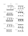
図7(a)〜図7(j)は、従来例に係る特許文献1に開示されたBGA基板を用いた半導体装置の製造工程中の半田ボール付け工程等を説明するための工程図である。 FIG. 7A to FIG. 7J are process diagrams for explaining a solder ball attaching process and the like during the manufacturing process of the semiconductor device using the BGA substrate disclosed in Patent Document 1 according to the conventional example. .
図7(a)〜図7(j)を参照すると、特許文献1には、半導体チップ、フィルムキャリア、あるいは基板31の電極パッド32に、フラックス22を転写装置により転写する方法であって、転写装置を構成する転写基板(転写治具)11は電極パッド32に対応する突起12を有し、転写基板11の突起12をフラックス浴21に浸して、フラックス22を突起12に付着させ、しかる後、転写基板11の突起12と電極パッド32の位置を合わせながら突起12を電極パッド32上に降下させて電極パッド32上にフラックス24を転写し、別に、電極パッド32の配列に対応した孔42を有する配列基板41を用いて孔42を介して半田ボール51を吸引保持し、半田ボール51と電極パッド32の位置を合わせながら配列基板41を基板31上に降下させて半田ボール51を電極パッド32上のフラックス24上に転写し、熱処理及び洗浄を行って基板31の電極パッド32と接合した半田バンプ52を形成する方法が開示されている。
Referring to FIGS. 7A to 7J, Patent Document 1 discloses a method of transferring a
特に、突起12は、高精度な金属加工によって形成されている。
In particular, the
特許文献1の転写基板41は、これが非常に精密な部品であることから高価であり、また半田ボールの数、サイズ、ピッチなどに応じて一品一葉で製作する必要があり、すなわち、半導体装置の各品種ごとに作る必要があり、半導体装置の製造コストを引き上げる大きな問題となっている。特に、突起12の加工には高精度が要求されるため、これが製造コストを引き上げる大きな要因となっている。
The
本発明の目的は、フラックスを製品基板上に正確に転写でき且つ転写にかかる製造コストを低下させるフラックス転写装置及びそれを用いたBGA基板を有する半導体装置の製造装置、並びにフラックス転写方法及びそれを用いたBGA基板を有する半導体装置の製造方法を提供することである。 SUMMARY OF THE INVENTION An object of the present invention is to provide a flux transfer apparatus that can accurately transfer a flux onto a product substrate and reduce manufacturing costs for the transfer, a semiconductor device manufacturing apparatus having a BGA substrate using the same, a flux transfer method, and It is to provide a method of manufacturing a semiconductor device having a used BGA substrate.
本発明は、第1の視点において、製品を構成する基板と同一種類のダミー基板と、前記ダミー基板上に前記製品を構成する基板上に配列される複数の電極と同様に配列された複数の電極と、前記複数の電極上にそれぞれ形成されフラックスが付着して該フラックスを保持するフラックス保持手段と、を有することを特徴とするフラックス転写装置を提供する。 In the first aspect, the present invention provides a dummy substrate of the same type as a substrate constituting a product, and a plurality of electrodes arranged in the same manner as a plurality of electrodes arranged on the substrate constituting the product on the dummy substrate. There is provided a flux transfer device comprising an electrode and a flux holding means formed on each of the plurality of electrodes to hold the flux by attaching a flux.
本発明は、第2の視点において、前記フラックス転写装置を用いることを特徴とするBGA基板を有する半導体装置の製造装置を提供する。 According to a second aspect of the present invention, there is provided a semiconductor device manufacturing apparatus having a BGA substrate, wherein the flux transfer apparatus is used.
本発明は、第3の視点において、製品を構成する基板と同一種類のダミー基板と、前記ダミー基板上に前記製品を構成する基板上に配列される複数の電極と同様に配列された複数の電極と、前記複数の電極上にそれぞれ形成されフラックスが付着して該フラックスを保持するフラックス保持手段と、を有するフラックス転写治具を用いたフラックス転写方法であって、前記フラックス保持手段の先端をフラックス浴に浸漬して該先端にフラックスを付着させる工程と、前記ダミー基板の前記フラックス保持手段に保持された前記フラックスを前記製品を構成する基板側の前記電極に転写する工程と、を含む、ことを特徴とするフラックス転写方法を提供する。 In a third aspect, the present invention provides a dummy substrate of the same type as a substrate constituting a product, and a plurality of electrodes arranged in the same manner as a plurality of electrodes arranged on the substrate constituting the product on the dummy substrate. A flux transfer method using a flux transfer jig having an electrode and a flux holding means formed on each of the plurality of electrodes to hold the flux by adhering to the flux, the tip of the flux holding means being Dipping in a flux bath to attach the flux to the tip; and transferring the flux held by the flux holding means of the dummy substrate to the electrode on the substrate side constituting the product, A flux transfer method is provided.
本発明は、第4の視点において、前記フラックス転写方法を用いることを特徴とするBGA基板を有する半導体装置の製造方法を提供する。 In a fourth aspect, the present invention provides a method for manufacturing a semiconductor device having a BGA substrate, wherein the flux transfer method is used.
本発明は、第5の視点において、半田ボールを搭載しようとするBGA基板の電極にフラックスを転写させる際、製品を構成する基板と同一種類のダミー基板の電極上にワイヤボンディング法によりバンプ又はピンを形成し、前記バンプ又は前記ピンを介して前記製品を構成する基板上の電極にフラックスを転写することを特徴とするBGA基板用のフラックス転写装置を提供する。 According to the fifth aspect of the present invention, when flux is transferred to an electrode of a BGA substrate on which a solder ball is to be mounted, a bump or pin is formed on a dummy substrate electrode of the same type as the substrate constituting the product by wire bonding. And a flux transfer device for a BGA substrate, wherein the flux is transferred to electrodes on the substrate constituting the product via the bumps or the pins.
本発明は、第6の視点において、半田ボールを搭載しようとするBGA基板の電極にフラックスを転写させる際、製品を構成する基板と同一種類のダミー基板の電極上にワイヤボンディング法によりバンプ又はピンを形成し、前記バンプ又は前記ピンを介して前記製品を構成する基板上の電極にフラックスを転写することを特徴とするBGA基板用のフラックス転写方法を提供する。 According to the sixth aspect of the present invention, in the sixth aspect, when flux is transferred to the electrode of the BGA substrate on which the solder ball is to be mounted, bumps or pins are formed on the electrodes of the same type of dummy substrate as the substrate constituting the product by wire bonding And a flux transfer method for a BGA substrate, wherein the flux is transferred to an electrode on a substrate constituting the product via the bumps or the pins.
本発明の効果を説明する。
(1)製品基板を転写用のダミー基板として兼用ないし転用し、製品基板と同様に電極が配列されているダミー基板を転写治具として用いることにより、新たに転写用の基板を設計する必要がなくされる。
(2)本発明のダミー基板は、その製作方法が簡便であるため、低コストでの製作が可能であり、BGA基板及びそれを用いた半導体装置の製造コストを低減させる。
(3)製品基板を転写用のダミー基板として兼用ないし転用することにより、製品基板とダミー基板では電極の位置が同じであるため、フラックスを製品基板上に正確に転写することができる。
(4)特に、ワイヤボンディング法により、ダミー基板上の電極にピン、突起又はワイヤを取り付けることにより、簡便、高精度かつ安価に転写治具ないし転写装置を作製することができる。
The effect of the present invention will be described.
(1) It is necessary to design a new transfer substrate by using the product substrate as a transfer dummy substrate and using the dummy substrate on which electrodes are arranged in the same manner as the product substrate as a transfer jig. Be lost.
(2) Since the manufacturing method of the dummy substrate of the present invention is simple, it can be manufactured at low cost, and the manufacturing cost of the BGA substrate and the semiconductor device using the same is reduced.
(3) By using the product substrate as a dummy substrate for transfer or diverting, the positions of the electrodes are the same on the product substrate and the dummy substrate, so that the flux can be accurately transferred onto the product substrate.
(4) In particular, by attaching pins, protrusions or wires to the electrodes on the dummy substrate by wire bonding, a transfer jig or transfer device can be produced simply, with high accuracy and at low cost.
本発明の好ましい実施の形態によれば、前記フラックス保持手段が、前記電極上に形成されたピンであり、好ましくは、前記ピンがロウ接により前記電極に取り付けられている。 According to a preferred embodiment of the present invention, the flux holding means is a pin formed on the electrode, and preferably the pin is attached to the electrode by brazing.
本発明の好ましい実施の形態によれば、前記フラックス保持手段が、前記電極上に形成されたバンプ状の突起であり、好ましくは、前記突起がワイヤボンディング法により前記電極に取り付けられている。 According to a preferred embodiment of the present invention, the flux holding means is a bump-like protrusion formed on the electrode, and preferably the protrusion is attached to the electrode by a wire bonding method.
本発明の好ましい実施の形態によれば、前記フラックス保持手段が、前記電極上に形成されたワイヤであり、好ましくは、前記ワイヤがワイヤボンディング法により前記電極に取り付けられている。 According to a preferred embodiment of the present invention, the flux holding means is a wire formed on the electrode, and preferably the wire is attached to the electrode by a wire bonding method.
本発明の好ましい実施の形態によれば、前記ワイヤがメッキ、さらに好ましくは、硬質の金属によりメッキされている。 According to a preferred embodiment of the present invention, the wire is plated, more preferably, a hard metal.
本発明の好ましい実施の形態によれば、前記製品を構成する基板が半導体装置のBGA基板、例えば、半導体チップを搭載するBGA基板である。 According to a preferred embodiment of the present invention, the substrate constituting the product is a BGA substrate of a semiconductor device, for example, a BGA substrate on which a semiconductor chip is mounted.
本発明をより詳しく説述するため、添付図面を参照して、本発明の一実施例を以下に説明する。 To describe the present invention in more detail, an embodiment of the present invention will be described below with reference to the accompanying drawings.
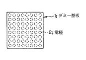
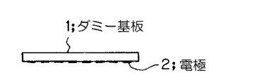
図1は、本発明の一実施例に係るBGA基板用のフラックス転写装置のダミー基板の平面図である。図2は、図1の正面図である。 FIG. 1 is a plan view of a dummy substrate of a flux transfer apparatus for a BGA substrate according to an embodiment of the present invention. FIG. 2 is a front view of FIG.
図1及び図2を参照すると、本発明の一実施例に係るフラックス転写装置は、製品を構成する基板(製品基板、半田ボールを搭載しようとする半導体装置のBGA基板)と同一種類ないし同様のダミー基板1を有する。 Referring to FIGS. 1 and 2, a flux transfer apparatus according to an embodiment of the present invention is the same or similar to a substrate constituting a product (product substrate, BGA substrate of a semiconductor device on which a solder ball is to be mounted). A dummy substrate 1 is provided.
転写治具となるダミー基板1上には、前記製品を構成する基板上に配列される複数の電極と同様に複数の電極2が配列されている。 On the dummy substrate 1 serving as a transfer jig, a plurality of electrodes 2 are arranged in the same manner as the plurality of electrodes arranged on the substrate constituting the product.
さらに、本発明の一実施例に係るフラックス転写装置は、予め、複数の電極2上にそれぞれ形成されフラックスが付着して該フラックスを保持するフラックス保持手段を有する。 Furthermore, the flux transfer apparatus according to an embodiment of the present invention has a flux holding unit that is formed in advance on each of the plurality of electrodes 2 and holds the flux by attaching the flux.
フラックス保持手段には、図3〜図5に示すようなピン、突起又はワイヤ等を適用することができる。 Pins, protrusions, wires or the like as shown in FIGS. 3 to 5 can be applied to the flux holding means.
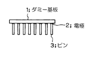
図3は、図1に示したダミー基板にピンを取り付けた様子を示す図である。 FIG. 3 is a diagram illustrating a state in which pins are attached to the dummy substrate illustrated in FIG. 1.
図3を参照すると、ダミー基板1上の電極2にピン3が取り付けられている。ピン3は、ロウ接により電極2に取り付けることができる。ピン3は、取付時、電極2上に自己整列する。 Referring to FIG. 3, pins 3 are attached to the electrodes 2 on the dummy substrate 1. The pin 3 can be attached to the electrode 2 by brazing. The pin 3 is self-aligned on the electrode 2 when installed.
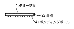
図4は、図1に示したダミー基板にバンプ状の突起、すなわち、ボンディングボールを取り付けた様子を示す図である。 FIG. 4 is a diagram illustrating a state in which bump-shaped protrusions, that is, bonding balls, are attached to the dummy substrate illustrated in FIG.
図4を参照すると、ダミー基板1上の電極2にボンディングボール(ボールバンプ)4が取り付けられている。ボンディングボール4は、半導体装置の製造において、チップ電極と外部配線のインナリードを電気的に接続するために用いられるワイヤボンディング法を応用したボールボンディング法により電極2に取り付けることができる。例えば、ワイヤ先端が溶製されてなるAu等の金属ボールを、加熱された電極2に拡散作用と超音波振動等による摩擦作用によって、接合する。ボンディングボール4は、取付時、電極2上に自己整列する。 Referring to FIG. 4, bonding balls (ball bumps) 4 are attached to the electrodes 2 on the dummy substrate 1. The bonding ball 4 can be attached to the electrode 2 by a ball bonding method applying a wire bonding method used for electrically connecting a chip electrode and an inner lead of an external wiring in the manufacture of a semiconductor device. For example, a metal ball such as Au having a wire tip melted is joined to the heated electrode 2 by a diffusion action and a friction action such as ultrasonic vibration. The bonding balls 4 are self-aligned on the electrodes 2 when attached.
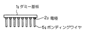
図5は、図1に示したダミー基板にワイヤを取り付けた様子を示す図である。 FIG. 5 is a diagram illustrating a state in which wires are attached to the dummy substrate illustrated in FIG. 1.
図5を参照すると、ダミー基板1上の電極2にボンディングワイヤ5が取り付けられている。ボンディングワイヤ5は、半導体装置の製造において、チップ電極と外部配線のインナリードを電気的に接続するために用いられるワイヤボンディング法により電極2に取り付けることができる。例えば、Au、AL又はAl−Si等のワイヤを電極2に、超音波併用熱圧着法(ボールボンディング法)により、或いは超音波法(ウェッジボンディング法)により、接合する。ボンディングワイヤ5は、取付時、電極2上に自己整列する。 Referring to FIG. 5, a bonding wire 5 is attached to the electrode 2 on the dummy substrate 1. The bonding wire 5 can be attached to the electrode 2 by a wire bonding method used for electrically connecting the chip electrode and the inner lead of the external wiring in the manufacture of the semiconductor device. For example, a wire such as Au, AL, or Al—Si is bonded to the electrode 2 by an ultrasonic thermocompression bonding method (ball bonding method) or an ultrasonic method (wedge bonding method). The bonding wire 5 is self-aligned on the electrode 2 when attached.
好ましくは、ボンディングワイヤ5をさらに、硬質金属によりめっきする。 Preferably, the bonding wire 5 is further plated with a hard metal.
図3に示したピン3が形成されたダミー基板1を、フラックス転写治具として利用する、フラックス転写方法について説明する。 A flux transfer method using the dummy substrate 1 on which the pins 3 shown in FIG. 3 are formed as a flux transfer jig will be described.
図6は、本発明の一実施例に係るフラックス転写方法を説明するための図である。 FIG. 6 is a diagram for explaining a flux transfer method according to an embodiment of the present invention.
図6を参照すると、ダミー基板1をフラックス浴中に降下させて、ピン3の先端にフラックス8を付着及び保持させ、次に、ダミー基板1を製品基板6上に移動して降下させ、ピン3に保持されたフラックス8を、製品基板6上の電極7に転写する。 Referring to FIG. 6, the dummy substrate 1 is lowered into the flux bath so that the flux 8 is attached and held on the tip of the pin 3, and then the dummy substrate 1 is moved onto the product substrate 6 to be lowered. 3 is transferred to the electrode 7 on the product substrate 6.
なお、製品基板6上の電極7に転写されたフラックス8上に、半田ボールを転写し半田バンプを形成する方法については、例えば、図7に示したような公知の方法を用いることができる。 As a method for forming solder bumps by transferring solder balls onto the flux 8 transferred to the electrodes 7 on the product substrate 6, for example, a known method as shown in FIG. 7 can be used.
本発明は、BGA基板等を有する半導体装置の製造に好適に適用される。 The present invention is suitably applied to the manufacture of a semiconductor device having a BGA substrate or the like.
1 ダミー基板
2 電極(ダミー基板上の電極)
3 ピン(フラックス保持手段)
4 ボンディングボール(フラックス保持手段)
5 ボンディングワイヤ(フラックス保持手段)
6 製品基板
7 電極(製品基板上の電極)
8 フラックス
1 Dummy substrate 2 Electrode (electrode on dummy substrate)
3 pins (flux holding means)
4 Bonding ball (flux holding means)
5 Bonding wire (flux holding means)
6 Product substrate 7 Electrode (electrode on product substrate)
8 Flux
Claims (24)
前記ダミー基板上に前記製品を構成する基板上に配列される複数の電極と同様に配列された複数の電極と、
前記複数の電極上にそれぞれ形成されフラックスが付着して該フラックスを保持するフラックス保持手段と、
を有することを特徴とするフラックス転写装置。 A dummy board of the same type as the board that constitutes the product;
A plurality of electrodes arranged in the same manner as a plurality of electrodes arranged on a substrate constituting the product on the dummy substrate;
A flux holding means that is formed on each of the plurality of electrodes and holds the flux by attaching the flux;
A flux transfer apparatus comprising:
前記フラックス保持手段の先端をフラックス浴に浸漬して該先端にフラックスを付着させる工程と、
前記ダミー基板の前記フラックス保持手段に保持された前記フラックスを前記製品を構成する基板側の前記電極に転写する工程と、
を含む、ことを特徴とするフラックス転写方法。 A dummy substrate of the same type as the substrate constituting the product, a plurality of electrodes arranged in the same manner as a plurality of electrodes arranged on the substrate constituting the product on the dummy substrate, and each on the plurality of electrodes A flux transfer method using a flux transfer jig having a flux holding means formed and attached to the flux.
Immersing the tip of the flux holding means in a flux bath to attach the flux to the tip;
Transferring the flux held by the flux holding means of the dummy substrate to the electrode on the substrate side constituting the product;
A flux transfer method comprising:
Priority Applications (1)
| Application Number | Priority Date | Filing Date | Title |
|---|---|---|---|
| JP2004105901A JP2005294447A (en) | 2004-03-31 | 2004-03-31 | Flux transfer apparatus, manufacturing apparatus of semiconductor device having BGA substrate using the same, flux transfer method, and manufacturing method of semiconductor device having BGA substrate using the same |
Applications Claiming Priority (1)
| Application Number | Priority Date | Filing Date | Title |
|---|---|---|---|
| JP2004105901A JP2005294447A (en) | 2004-03-31 | 2004-03-31 | Flux transfer apparatus, manufacturing apparatus of semiconductor device having BGA substrate using the same, flux transfer method, and manufacturing method of semiconductor device having BGA substrate using the same |
Publications (1)
| Publication Number | Publication Date |
|---|---|
| JP2005294447A true JP2005294447A (en) | 2005-10-20 |
Family
ID=35327062
Family Applications (1)
| Application Number | Title | Priority Date | Filing Date |
|---|---|---|---|
| JP2004105901A Withdrawn JP2005294447A (en) | 2004-03-31 | 2004-03-31 | Flux transfer apparatus, manufacturing apparatus of semiconductor device having BGA substrate using the same, flux transfer method, and manufacturing method of semiconductor device having BGA substrate using the same |
Country Status (1)
| Country | Link |
|---|---|
| JP (1) | JP2005294447A (en) |
-
2004
- 2004-03-31 JP JP2004105901A patent/JP2005294447A/en not_active Withdrawn
Similar Documents
| Publication | Publication Date | Title |
|---|---|---|
| TWI549204B (en) | Manufacturing method of semiconductor device | |
| JPH09134934A (en) | Semiconductor package and semiconductor device | |
| US8046911B2 (en) | Method for mounting electronic component on substrate and method for forming solder surface | |
| TW201505145A (en) | Semiconductor device and method of manufacturing same | |
| JPS5835935A (en) | Semiconductor device and manufacture thereof | |
| JP2006128711A (en) | Semiconductor device and manufacturing method thereof | |
| US6852571B2 (en) | Method of manufacturing stacked semiconductor device | |
| JP4586583B2 (en) | Semiconductor device bonding method | |
| US20060027899A1 (en) | Structure with spherical contact pins | |
| JP2005294447A (en) | Flux transfer apparatus, manufacturing apparatus of semiconductor device having BGA substrate using the same, flux transfer method, and manufacturing method of semiconductor device having BGA substrate using the same | |
| JP3887993B2 (en) | Connection method between IC chip and circuit board | |
| JPH10233417A (en) | Semiconductor device and manufacturing method thereof | |
| JP2008060483A (en) | Semiconductor device mounting structure and method of manufacturing the same | |
| JP2008192833A (en) | Manufacturing method of semiconductor device | |
| JP3855532B2 (en) | Connection method between IC chip and circuit board | |
| JP3707516B2 (en) | Semiconductor element mounting method and element mounting sheet used therefor | |
| JP2000012621A (en) | Semiconductor device and method of manufacturing the same | |
| JP3645444B2 (en) | Manufacturing method of semiconductor integrated circuit device | |
| JP3704229B2 (en) | Method and apparatus for manufacturing semiconductor device | |
| JPH11317424A (en) | Semiconductor device mounting method and mounting structure | |
| JP3674550B2 (en) | Semiconductor device | |
| JP2002324878A (en) | Adapter for changing semiconductor device terminal and semiconductor device using it and mounting method therefor | |
| JP4729438B2 (en) | Semiconductor device and manufacturing method thereof | |
| JPH0685003A (en) | Semiconductor device and its production | |
| JP2010141112A (en) | Semiconductor device and method of manufacturing semiconductor device |
Legal Events
| Date | Code | Title | Description |
|---|---|---|---|
| A300 | Application deemed to be withdrawn because no request for examination was validly filed |
Free format text: JAPANESE INTERMEDIATE CODE: A300 Effective date: 20070605 |