JP2005294432A - Electrolytic capacitor and its manufacturing method - Google Patents
Electrolytic capacitor and its manufacturing method Download PDFInfo
- Publication number
- JP2005294432A JP2005294432A JP2004105553A JP2004105553A JP2005294432A JP 2005294432 A JP2005294432 A JP 2005294432A JP 2004105553 A JP2004105553 A JP 2004105553A JP 2004105553 A JP2004105553 A JP 2004105553A JP 2005294432 A JP2005294432 A JP 2005294432A
- Authority
- JP
- Japan
- Prior art keywords
- electrode layer
- electrolytic capacitor
- polymer
- layer
- film
- Prior art date
- Legal status (The legal status is an assumption and is not a legal conclusion. Google has not performed a legal analysis and makes no representation as to the accuracy of the status listed.)
- Granted
Links
Images

Landscapes
- Fixed Capacitors And Capacitor Manufacturing Machines (AREA)
Abstract
Description
本発明は、固体電解質層を備えた電解コンデンサおよびその製造方法に関する。 The present invention relates to an electrolytic capacitor including a solid electrolyte layer and a method for manufacturing the same.
近年、高周波用途に適した電子部品のうちの1つとして、多様な電子機器に電解コンデンサが搭載されている。この電解コンデンサに関しては、例えば、電子機器のデジタル化、小型化および高速化が加速的に進行している情勢下において、大容量化や低インピーダンス化が要望されていると共に、動作安定性や動作信頼性の確保、ならびに高寿命化も併せて要望されている。 In recent years, electrolytic capacitors are mounted on various electronic devices as one of electronic components suitable for high-frequency applications. With regard to this electrolytic capacitor, for example, in a situation where the digitization, downsizing and speeding up of electronic devices are accelerating, there is a demand for large capacity and low impedance, as well as operational stability and operation. There is also a demand for ensuring reliability and extending the service life.
電解コンデンサの主要部(コンデンサ素子)は、例えば、弁作用金属により構成された陽極と、この陽極の表層が陽極酸化されることにより形成された酸化皮膜(誘電体層)と、電解質層と、陰極とがこの順に積層された積層構造を有している。 The main part (capacitor element) of the electrolytic capacitor includes, for example, an anode made of a valve metal, an oxide film (dielectric layer) formed by anodizing the surface layer of the anode, an electrolyte layer, The cathode has a laminated structure in which the cathode is laminated in this order.
この電解コンデンサは、主に、電解質層の種類に応じて2種類に大別される。すなわち、液体材料により構成された電解質層(電解液)を含んでコンデンサ素子が構成され、主にイオン伝導性を利用した導電機構を有する液体電解コンデンサと、錯塩や導電性高分子などの固体材料により構成された電解質層(固体電解質層)を含んでコンデンサ素子が構成され、主に電子伝導性を利用した導電機構を有する固体電解コンデンサである。これらの2種類の電解コンデンサを作動特性の安定性の観点において比較すると、例えば、液体電解コンデンサでは電解液の漏洩や蒸発に起因して作動特性が経時劣化し得るのに対して、この電解液の漏洩や蒸発に起因する作動特性の経時劣化は固体電解コンデンサでは起こり得ないため、今後主流になり得る電解コンデンサとして、最近では液体電解コンデンサに代えて固体電解コンデンサに関する研究開発が活発に進められている。この固体電解コンデンサに関する研究過程では、例えば、漏れ電流特性、インピーダンス特性ならびに耐熱特性などの一連の作動特性を考慮して、固体電解質層の主要部が二酸化マンガンや錯塩から共役系の導電性高分子に急速に移行しつつある。 This electrolytic capacitor is mainly divided into two types according to the type of the electrolyte layer. That is, a capacitor element is formed including an electrolyte layer (electrolyte) made of a liquid material, and has a conductive mechanism mainly utilizing ion conductivity, and a solid material such as a complex salt or a conductive polymer The capacitor element is configured to include the electrolyte layer (solid electrolyte layer) configured by the above, and is a solid electrolytic capacitor having a conductive mechanism mainly utilizing electronic conductivity. When these two types of electrolytic capacitors are compared in terms of stability of operating characteristics, for example, in liquid electrolytic capacitors, the operating characteristics may deteriorate over time due to leakage or evaporation of the electrolytic solution. As the electrolytic capacitors that can become the mainstream in the future are recently being actively researched and developed for solid electrolytic capacitors instead of liquid electrolytic capacitors, the deterioration of the operating characteristics due to leakage and evaporation of the liquid cannot occur with solid electrolytic capacitors. ing. In this research process on solid electrolytic capacitors, for example, considering the series of operating characteristics such as leakage current characteristics, impedance characteristics, and heat resistance characteristics, the main part of the solid electrolyte layer is composed of manganese dioxide or complex salts and conjugated conductive polymers. Is moving rapidly.
この固体電解コンデンサに関しては、特に、以下で説明する技術的背景に基づき、短絡時の発熱に起因して破壊されること(発火や燃焼を含む)を防止するために、所定の温度範囲内において温度の上昇に応じて抵抗が上昇する機能(いわゆるPTC(Positive Temperature Coefficient)機能)が要望されている。 With respect to this solid electrolytic capacitor, in particular, based on the technical background described below, in order to prevent destruction (including ignition and combustion) due to heat generation at the time of a short circuit, within a predetermined temperature range There is a demand for a function (so-called PTC (Positive Temperature Coefficient) function) in which the resistance increases with an increase in temperature.
すなわち、固体電解コンデンサは、上記したように多様な電子機器(電子回路)に搭載されており、一般に故障率が低い点において利点を有している。ところが、例えば、電子回路上のトラブルに起因して固体電解コンデンサに過電圧(定格電圧よりも大きい電圧)や逆電圧(正負が逆の電圧)が印加された場合に、それらの過電圧や逆電圧に起因して誘電体層が部分的に破損すると、陽極と固体電解質層および陰極とが意図せずに導通するため、固体電解コンデンサが短絡してしまう。この短絡が発生した場合に、固体電解コンデンサに過電流(短絡電流)が流れると、その固体電解コンデンサが発熱し、場合によっては発熱に起因して発火または燃焼することにより破壊されてしまう。 That is, the solid electrolytic capacitor is mounted on various electronic devices (electronic circuits) as described above, and generally has an advantage in that the failure rate is low. However, for example, when an overvoltage (a voltage greater than the rated voltage) or a reverse voltage (a voltage that is opposite in positive and negative) is applied to the solid electrolytic capacitor due to a problem in the electronic circuit, the overvoltage or reverse voltage When the dielectric layer is partially damaged due to this, the anode, the solid electrolyte layer, and the cathode are unintentionally conducted, and the solid electrolytic capacitor is short-circuited. When this short circuit occurs, if an overcurrent (short circuit current) flows through the solid electrolytic capacitor, the solid electrolytic capacitor generates heat, and in some cases, the solid electrolytic capacitor is destroyed by firing or burning.
この固体電解コンデンサの短絡時の発熱に起因する破壊を防止すると共に、固体電解コンデンサと共に電子回路に搭載されている回路部品の破壊も併せて防止する対策としては、例えば、固体電解コンデンサにヒューズを搭載する技術が考えられる。このヒューズを搭載した固体電解コンデンサとしては、例えば、陰極と陰極リード(通電用のリード)とがヒューズを介して電気的に接続された構成を有するものが知られている。この種の固体電解コンデンサでは、短絡時の発熱に起因してヒューズが溶解切断されることにより回路機構が遮断され、すなわち過電流の電流経路が遮断されるため、固体電解コンデンサの破壊が防止される。ところが、ヒューズを利用した固体電解コンデンサでは、そのヒューズの構造的および機構的要因に起因していくつかの問題がある。第1に、固体電解コンデンサにヒューズを搭載すると、その固体電解コンデンサの構造が複雑化かつ大型化してしまう。第2に、ヒューズは機械的強度が弱く、すなわちヒューズは取り扱いが困難なため、固体電解コンデンサの製造工程が複雑化すると共に製造歩留まりが低下してしまう。第3に、ヒューズを搭載した固体電解コンデンサでは、場合によっては信頼性の観点において不安がある。具体的には、例えば、ヒューズの周囲がモールド樹脂で強固に覆われている場合には、短絡時の発熱に起因してヒューズが溶解したとしても、そのヒューズがモールド樹脂の存在に起因して完全に切断されない可能性があるため、依然として回路機構が遮断されない場合に固体電解コンデンサが破壊されるおそれがある。したがって、固体電解コンデンサの破壊防止に関する信頼性を高めるために、ヒューズに代わる安全機構が模索されており、その安全機構としてPTC機能が要望されているのである。 As a measure to prevent destruction due to heat generation at the time of short-circuiting of this solid electrolytic capacitor and also prevent destruction of circuit components mounted on the electronic circuit together with the solid electrolytic capacitor, for example, a fuse is attached to the solid electrolytic capacitor. The technology to be installed can be considered. As a solid electrolytic capacitor equipped with this fuse, for example, a capacitor having a configuration in which a cathode and a cathode lead (a lead for energization) are electrically connected via a fuse is known. In this type of solid electrolytic capacitor, the circuit mechanism is cut off by melting and cutting the fuse due to heat generation at the time of short circuit, that is, the overcurrent current path is cut off, so that destruction of the solid electrolytic capacitor is prevented. The However, a solid electrolytic capacitor using a fuse has several problems due to structural and mechanical factors of the fuse. First, when a fuse is mounted on a solid electrolytic capacitor, the structure of the solid electrolytic capacitor becomes complicated and large. Secondly, the fuse has a low mechanical strength, that is, the fuse is difficult to handle, which complicates the manufacturing process of the solid electrolytic capacitor and decreases the manufacturing yield. Thirdly, solid electrolytic capacitors equipped with fuses may be anxious in terms of reliability. Specifically, for example, when the periphery of the fuse is firmly covered with mold resin, even if the fuse is melted due to heat generation at the time of short circuit, the fuse is caused by the presence of mold resin. Since it may not be completely disconnected, the solid electrolytic capacitor may be destroyed if the circuit mechanism is still not interrupted. Therefore, in order to increase the reliability regarding prevention of destruction of the solid electrolytic capacitor, a safety mechanism replacing the fuse is being sought, and a PTC function is desired as the safety mechanism.
このPTC機能を有する電解コンデンサとしては、既にいくつかの態様を有するものが提案されている。具体的には、例えば、PTCサーミスタがコンデンサ素子に対向配置され、それらのPTCサーミスタおよびコンデンサ素子がモールド樹脂で覆われた構成を有するものが知られている(例えば、特許文献1参照。)。なお、この電解コンデンサでは、ヒューズに代わる安全機構としてPTCサーミスタが設けられているわけではない。また、例えば、コンデンサ素子の陽極(内部端子)と陽極リード(外部端子)とがPTCサーミスタ(半導体セラミック層)を介して電気的に接続された構成を有するものが知られている(例えば、特許文献2参照。)。さらに、例えば、コンデンサ素子の一方の電極(外部電極)と電極リード(金属端子)とがPTCサーミスタ(PTC機能を有する過電流・過熱保護素子)を介して電気的に接続された構成を有するものが知られている(例えば、特許文献3参照。)。
ところで、PTC機能を有する固体電解コンデンサの製造工程では、固体電解コンデンサの製造歩留まりを高めることにより生産性を確保するために、その固体電解コンデンサを可能な限り安定に製造する必要がある。しかしながら、従来の固体電解コンデンサの製造方法では、PTC機能を付与することにより短絡時の発熱に起因する固体電解コンデンサの破壊は防止されるが、例えば、コンデンサ素子にPTCサーミスタを熱圧着して接続させようとすると、その熱圧着時に生じる力学的要因(コンデンサ素子に加わる過度な外力)に起因して誘電体層が著しく破損しやすいため、製造途中において固体電解コンデンサが力学的に破壊されるおそれがあった。この固体電解コンデンサの力学的な破壊は、短絡時の発熱に起因する固体電解コンデンサの破壊とは異なり、その固体電解コンデンサの基本構造自体が損なわれる致命的なものであるため、もはやPTC機能を利用して防止し得るものではない。固体電解コンデンサが製造途中で力学的に破壊されると、当然ながら、製造歩留まりが低下することにより固体電解コンデンサの生産性を確保し得ないため、固体電解コンデンサを安定に製造することが困難になる。したがって、PTC機能を利用して短絡時の発熱に起因する破壊を防止しつつ、固体電解コンデンサの製造歩留まりを高めることにより生産性を確保するためには、そのPTC機能を有する固体電解コンデンサを可能な限り安定に製造することが可能な技術の確立が急務である。特に、PTC機能を有する固体電解コンデンサを可能な限り安定に製造することが可能な技術を確立する場合には、固体電解コンデンサの量産性を考慮して、その固体電解コンデンサを可能な限り容易に製造することが可能であることも重要である。 By the way, in the manufacturing process of a solid electrolytic capacitor having a PTC function, it is necessary to manufacture the solid electrolytic capacitor as stably as possible in order to secure productivity by increasing the manufacturing yield of the solid electrolytic capacitor. However, in the conventional method of manufacturing a solid electrolytic capacitor, destruction of the solid electrolytic capacitor due to heat generation at the time of a short circuit can be prevented by providing a PTC function. For example, a PTC thermistor is connected to a capacitor element by thermocompression bonding. Doing so may cause the dielectric layer to be significantly damaged due to mechanical factors (excessive external force applied to the capacitor element) generated during thermocompression bonding. was there. Unlike the breakdown of the solid electrolytic capacitor caused by the heat generated at the time of short circuit, the mechanical breakdown of the solid electrolytic capacitor is a fatal damage to the basic structure of the solid electrolytic capacitor itself. It cannot be prevented by using it. If a solid electrolytic capacitor is mechanically destroyed during manufacturing, it is of course difficult to secure the productivity of the solid electrolytic capacitor because the yield of the solid electrolytic capacitor is lowered and the productivity of the solid electrolytic capacitor cannot be secured. Become. Therefore, in order to ensure the productivity by increasing the production yield of the solid electrolytic capacitor while preventing the destruction due to the heat generation at the time of short circuit using the PTC function, the solid electrolytic capacitor having the PTC function is possible. There is an urgent need to establish a technology that can be manufactured as stably as possible. In particular, when establishing a technology capable of manufacturing a solid electrolytic capacitor having a PTC function as stably as possible, considering the mass productivity of the solid electrolytic capacitor, the solid electrolytic capacitor can be made as easy as possible. It is also important that it can be manufactured.
本発明はかかる問題点に鑑みてなされたもので、その第1の目的は、PTC機能を有する電解コンデンサが製造途中において力学的に破壊されることを防止することにより、そのPTC機能を有する電解コンデンサを可能な限り安定かつ容易に製造することが可能な電解コンデンサの製造方法を提供することにある。 The present invention has been made in view of such problems, and a first object of the present invention is to prevent an electrolytic capacitor having a PTC function from being mechanically destroyed in the course of manufacturing, thereby providing an electrolytic process having the PTC function. An object of the present invention is to provide an electrolytic capacitor manufacturing method capable of manufacturing a capacitor as stably and easily as possible.
また、本発明の第2の目的は、PTC機能を利用して短絡時の発熱に起因する破壊を可能な限り防止することが可能な電解コンデンサを提供することにある。 A second object of the present invention is to provide an electrolytic capacitor capable of preventing destruction due to heat generation at the time of a short circuit as much as possible using the PTC function.
本発明に係る電解コンデンサは、第1の電極層と、誘電体層と、固体電解質層と、その固体電解質層の表面において液状材料が膜化されることにより形成され、所定の温度範囲内において温度の上昇に応じて抵抗が上昇する第2の電極層とがこの順に積層された積層構造を有するものである。 The electrolytic capacitor according to the present invention is formed by forming a liquid material on the surface of the first electrode layer, the dielectric layer, the solid electrolyte layer, and the solid electrolyte layer, and within a predetermined temperature range. The second electrode layer whose resistance increases with an increase in temperature has a stacked structure in which the second electrode layer is stacked in this order.
本発明に係る電解コンデンサでは、所定の温度範囲内において温度の上昇に応じて抵抗が上昇する第2の電極層の機能(いわゆるPTC機能)を利用して、短絡時の発熱に起因する破壊が防止される。 In the electrolytic capacitor according to the present invention, the function due to the second electrode layer (so-called PTC function) in which the resistance increases as the temperature rises within a predetermined temperature range is used, and the breakdown due to the heat generation at the time of short-circuiting occurs. Is prevented.
本発明に係る電解コンデンサの製造方法は、第1の電極層、誘電体層および固体電解質層がこの順に積層された積層構造のうちの固体電解質の表面に液状材料を供給して膜化することにより、所定の温度範囲内において温度の上昇に応じて抵抗が上昇するように第2の電極層を形成したものである。 The method for producing an electrolytic capacitor according to the present invention includes forming a film by supplying a liquid material to the surface of a solid electrolyte in a laminated structure in which a first electrode layer, a dielectric layer, and a solid electrolyte layer are laminated in this order. Thus, the second electrode layer is formed so that the resistance increases as the temperature rises within a predetermined temperature range.
本発明に係る電解コンデンサの製造方法では、固体電解質層に所定の温度範囲内において温度の上昇に応じて抵抗が上昇する機能(いわゆるPTC機能)を有するように第2の電極層が形成される際に、その固体電解質層の表面に液状材料が供給されて膜化されることにより第2の電極層が形成される。電解コンデンサにPTCサーミスタを熱圧着する際に、その熱圧着時に生じる力学的要因(電解コンデンサに加わる過度な外力)に起因して誘電体層が著しく破損しやすい場合とは異なり、製造途中において誘電体層に大きな外力が加わらないため、その誘電体層が製造途中において力学的要因に起因して破損しにくくなる。 In the method for producing an electrolytic capacitor according to the present invention, the second electrode layer is formed in the solid electrolyte layer so as to have a function (so-called PTC function) in which the resistance increases as the temperature rises within a predetermined temperature range. At this time, a liquid material is supplied to the surface of the solid electrolyte layer to form a film, thereby forming the second electrode layer. When thermocompression bonding a PTC thermistor to an electrolytic capacitor, the dielectric layer is prone to breakage due to mechanical factors (excessive external force applied to the electrolytic capacitor) generated during the thermocompression bonding. Since a large external force is not applied to the body layer, the dielectric layer is less likely to be damaged due to mechanical factors during manufacture.
特に、本発明に係る電解コンデンサでは、第2の電極層が、2層以上の層が積層された積層構造を有し、その2層以上の層のうちの少なくとも1つの層において所定の温度範囲内において温度の上昇に応じて抵抗が上昇してもよいし、あるいは単層構造を有していてもよい。第2の電極層が積層構造を有する場合には、導電性を確保するための主電極層と、その主電極層と固体電解質層との間に配設され、主電極層を固体電解質層に電気的に接合させるための副電極層とを含む2層構造を有し、主電極層が金属を含んで構成され、副電極層がカーボンを含んで構成されていてもよい。この場合には、所定の温度範囲内において温度の上昇に応じて抵抗を上昇させるための液状材料が導電性粒子を含む液状高分子であり、第2の電極層が液状高分子が膜化されることにより形成された膜状高分子と、その膜状高分子中に保持された導電性粒子とを含んで構成されているのが好ましく、その液状高分子が熱硬化性高分子および可溶性熱可塑性高分子のうちの少なくとも1種を含んでいるのが好ましい。特に、第2の電極層が60℃以上150℃以下の温度範囲内において抵抗が1000倍以上上昇するものであるのが好ましい。なお、第1の電極層が弁作用金属を含んで構成され、誘電体層が第1の電極層の表層が陽極酸化されることにより形成されたものであってもよい。 Particularly, in the electrolytic capacitor according to the present invention, the second electrode layer has a laminated structure in which two or more layers are laminated, and at least one of the two or more layers has a predetermined temperature range. The resistance may increase in accordance with the temperature rise, or may have a single layer structure. When the second electrode layer has a laminated structure, it is disposed between the main electrode layer for ensuring conductivity and the main electrode layer and the solid electrolyte layer, and the main electrode layer is formed as a solid electrolyte layer. It may have a two-layer structure including a sub-electrode layer for electrical connection, the main electrode layer may include a metal, and the sub-electrode layer may include carbon. In this case, the liquid material for increasing the resistance in response to the temperature rise within a predetermined temperature range is a liquid polymer containing conductive particles, and the liquid polymer is formed into the second electrode layer. It is preferable that the liquid polymer is composed of a thermosetting polymer and a soluble heat polymer, and a conductive polymer held in the film polymer. It preferably contains at least one kind of plastic polymer. In particular, the resistance of the second electrode layer is preferably increased 1000 times or more within a temperature range of 60 ° C. or more and 150 ° C. or less. The first electrode layer may include a valve metal, and the dielectric layer may be formed by anodizing the surface layer of the first electrode layer.
また、本発明に係る電解コンデンサの製造方法では、所定の温度範囲内において温度の上昇に応じて抵抗を上昇させるための液状材料として導電性粒子を含む液状高分子を使用し、液状高分子が膜化した膜状高分子と、その膜状高分子中に保持された導電性粒子とを含むように第2の電極層を形成するのが好ましく、その液状高分子として熱硬化性高分子および可溶性熱可塑性高分子のうちの少なくとも1種を含む材料を使用するのが好ましい。 Further, in the method for manufacturing an electrolytic capacitor according to the present invention, a liquid polymer containing conductive particles is used as a liquid material for increasing resistance in response to a temperature rise within a predetermined temperature range. It is preferable to form the second electrode layer so as to include a film-like polymer formed into a film and conductive particles held in the film-like polymer. As the liquid polymer, a thermosetting polymer and It is preferred to use a material comprising at least one of the soluble thermoplastic polymers.
なお、「液状材料」とは、室温(意図的に設定された高温環境を除き、一般的に電解コンデンサの製造工程が実施される通常環境の雰囲気温度であり、具体的には約15℃以上30℃以下の範囲内の雰囲気温度)において溶媒を利用せずに直接的、あるいは溶媒を利用して(溶媒に溶解されることにより)間接的に液体状態(流動状態)となり、塗布法、浸漬法または印刷法などの手法を使用して固体電解質層の表面に供給されることにより直接的に膜化可能な特性を有する材料である。上記した「液体状態(流動状態)」とは、固体電解質層の表面に供給可能な限りにおいてペースト状態なども含む概念であり、例えば、約100cP以上1000000cP以下の範囲内の粘度を有する状態である。また、「液状高分子」とは、上記した「液状材料」と同様の特性を有する高分子であり、具体的には、不溶性熱可塑性高分子(室温において直接的に液体状態にならない上、室温において溶解可能な溶媒が存在しないために間接的にも液体状態にならない熱可塑性高分子)を除き、上記した熱硬化性高分子や可溶性熱可塑性高分子(室温において直接的に液体状態にならないが、室温において溶解可能な溶媒が存在するために間接的に液体状態になる熱可塑性高分子)である。 “Liquid material” means room temperature (excluding the intentionally set high temperature environment, generally the ambient temperature of the normal environment where the electrolytic capacitor manufacturing process is carried out, specifically about 15 ° C. or more. (At atmospheric temperature within the range of 30 ° C. or lower), without using a solvent, or indirectly (by being dissolved in a solvent) using a solvent to be in a liquid state (flowing state). It is a material having a property that can be directly formed into a film by being supplied to the surface of the solid electrolyte layer using a method such as a printing method or a printing method. The above-mentioned “liquid state (fluid state)” is a concept including a paste state as long as it can be supplied to the surface of the solid electrolyte layer, and has a viscosity in a range of about 100 cP to 1000000 cP, for example. . The “liquid polymer” is a polymer having the same characteristics as the above-mentioned “liquid material”. Specifically, it is an insoluble thermoplastic polymer (not directly in a liquid state at room temperature and at room temperature). In addition to the above-mentioned thermosetting polymers and soluble thermoplastic polymers (which do not directly become liquid at room temperature, except for thermoplastic polymers that do not indirectly become liquid because there is no soluble solvent) , A thermoplastic polymer that is indirectly in a liquid state due to the presence of a solvent that is soluble at room temperature.
本発明に係る電解コンデンサによれば、所定の温度範囲内において温度の上昇に応じて抵抗が上昇する第2の電極層の機能(いわゆるPTC機能)に基づき、短絡時の発熱に起因して破壊されにくくなるため、そのPTC機能を利用して短絡時の発熱に起因する破壊を可能な限り防止することができる。 According to the electrolytic capacitor of the present invention, breakdown is caused due to heat generation at the time of short circuit based on the function of the second electrode layer (so-called PTC function) in which the resistance increases in response to the temperature rise within a predetermined temperature range. Therefore, the PTC function can be used to prevent damage caused by heat generation during a short circuit as much as possible.
本発明に係る電解コンデンサの製造方法によれば、固体電解質層に所定の温度範囲内において温度の上昇に応じて抵抗が上昇する機能(いわゆるPTC機能)を有するように第2の電極層が形成される際に、その固体電解質層の表面に液状材料が供給されて膜化されることにより第2の電極層が形成されることに基づき、製造途中において誘電体層が力学的要因に起因して破損しにくくなるため、PTC機能を有する電解コンデンサが製造途中において力学的に破壊されることを防止することにより、そのPTC機能を有する電解コンデンサを可能な限り安定かつ容易に製造することができる。 According to the method for manufacturing an electrolytic capacitor according to the present invention, the second electrode layer is formed so that the solid electrolyte layer has a function (so-called PTC function) in which the resistance increases as the temperature rises within a predetermined temperature range. In this case, the dielectric layer is caused by mechanical factors during the manufacturing process based on the fact that the second electrode layer is formed by supplying a liquid material to the surface of the solid electrolyte layer to form a film. Therefore, it is possible to manufacture the electrolytic capacitor having the PTC function as stably and easily as possible by preventing the electrolytic capacitor having the PTC function from being mechanically destroyed during the manufacturing. .
以下、本発明の実施の形態について、図面を参照して詳細に説明する。 Hereinafter, embodiments of the present invention will be described in detail with reference to the drawings.
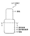
まず、図1および図2を参照して、本発明の一実施の形態に係る電解コンデンサの構成について簡単に説明する。図1および図2は電解コンデンサの主要部(コンデンサ素子10)の構成を表しており、図1は外観構成を示し、図2は図1に示したII−II線に沿った断面構成を拡大して示している。 First, with reference to FIG. 1 and FIG. 2, the structure of the electrolytic capacitor which concerns on one embodiment of this invention is demonstrated easily. 1 and 2 show the configuration of the main part (capacitor element 10) of the electrolytic capacitor, FIG. 1 shows the external configuration, and FIG. 2 is an enlarged cross-sectional configuration along the line II-II shown in FIG. As shown.
この電解コンデンサは、図1および図2に示したコンデンサ素子10に陽極リードおよび陰極リード(いずれも図示せず)が接続され、それらの陽極リードおよび陰極リードの双方が部分的に露出するようにコンデンサ素子10がモールド樹脂(図示せず)により周囲を覆われた構造を有するものである。コンデンサ素子10は、電解コンデンサの主要部として電気的反応を生じるものであり、例えば、図1および図2に示したように、陽極11と、この陽極11の周囲(一端部)を部分的に覆うように配設された誘電体層12と、この誘電体層12を覆うように配設された固体電解質層13と、この固体電解質層13を覆うように配設された陰極14とを含み、すなわち陽極11、誘電体層12、固体電解質層13および陰極14がこの順に積層された積層構造を有している。
In this electrolytic capacitor, an anode lead and a cathode lead (both not shown) are connected to the
陽極11は、拡面化(または粗面化)された表面凹凸構造を有する第1の電極層であり、例えば、アルミニウム(Al)、チタン(Ti)、タンタル(Ta)またはニオブ(Nb)などの弁作用金属を含んで構成されている。具体的には、陽極11は、例えば、アルミニウムまたはチタンなどの金属箔や、タンタルまたはニオブなどの金属焼結体である。なお、拡面化された陽極11の表面凹凸構造の詳細に関しては後述する(図3参照)。
The
誘電体層12は、例えば、弁作用金属により構成された陽極11の表層が陽極酸化されることにより形成された酸化皮膜である。この誘電体層12は、例えば、陽極11がアルミニウムより構成されている場合には、酸化アルミニウム(Al2 O3 )により構成されている。
The
固体電解質層13は、例えば、導電性高分子と、この導電性高分子の導電率を制御するためのドーパントとを含み、すなわち導電性高分子にドーパントが含有(ドープ)された構成を有している。導電性高分子は、例えば、ポリアニリン、ポリピロール、ポリチオフェン、ポリフランおよびこれらの誘導体を含む群のうちの少なくとも1種により構成されており、具体的な一例を挙げれば、ポリチオフェンの誘導体であるポリエチレンジオキシチオフェンなどにより構成されている。また、ドーパントは、例えば、アルキルベンゼンスルホン酸およびその塩、アルキルナフタレンスルホン酸およびその塩、ならびにリン酸を含む群のうちの少なくとも1種により構成されており、具体的な一例を挙げれば、パラトルエンスルホン酸鉄またはイソピロピルナフタレンスルホン酸鉄などにより構成されている。この固体電解質層13を含んでコンデンサ素子10が構成されている電解コンデンサは、いわゆる固体電解コンデンサである。
The
陰極14は、誘電体層12および固体電解質層13を挟んで陽極11に対向配置された第2の電極層である。この陰極14は、固体電解質層13の表面において液状材料が膜化されることにより形成されたものであり、所定の温度範囲内において温度の上昇に応じて抵抗が上昇し、より具体的には抵抗が指数関数的に上昇する機能(いわゆるPTC機能)を有している。特に、PTC機能を有する陰極14は、例えば、約60℃以上150℃以下の範囲内において抵抗が(常温の抵抗と比較して)約1000倍以上上昇するものである。「液状材料」とは、室温(意図的に設定された高温環境を除き、一般的に電解コンデンサの製造工程が実施される通常環境の雰囲気温度であり、具体的には約15℃以上30℃以下の範囲内の雰囲気温度)において溶媒を利用せずに直接的、あるいは溶媒を利用して(溶媒に溶解されることにより)間接的に液体状態(流動状態)となり、塗布法、浸漬法または印刷法などの手法を使用して固体電解質層13の表面に供給されることにより直接的に膜化可能な特性を有する材料である。上記した「液体状態(流動状態)」とは、固体電解質層13の表面に供給可能な限りにおいてペースト状態なども含む概念であり、例えば、約100cP以上1000000cP以下の範囲内の粘度を有する状態である。
The
特に、陰極14は、例えば、2層以上の層が積層された積層構造を有しており、その2層以上の層のうちの少なくとも1つの層においてPTC機能を有している。具体的には、陰極14は、例えば、図2に示したように、導電性を確保するための主電極層14Bと、その主電極層14Bと固体電解質層13との間に配設され、主電極層14Bを固体電解質層13に電気的に接合させるための副電極層14Aとを含み、すなわち副電極層14A上に主電極層14Bが配置された2層構造を有している。この陰極14では、例えば、副電極層14AがPTC機能を有しておらず、主電極層14BのみがPTC機能を有している。
In particular, the
副電極層14Aは、例えば、カーボンを含んで構成されており、具体的には固体電解質層13の表面において液状材料(カーボンペースト)が膜化されることにより形成されたものである。なお、副電極層14Aは、上記したように主電極層14Bを固体電解質層13に電気的に接合させる機能の他に、例えば、主電極層14Bを固体電解質層13に直接的に接触させた場合に、高温高湿環境中において主電極層14B中の特定成分(例えば銀(Ag))のマイグレーションを防止する機能も有している。
For example, the
主電極層14Bは、例えば、金属を含んで構成されており、具体的には副電極層14Aの表面において液状材料(金属ペースト)が膜化されることにより形成されたものである。より具体的には、主電極層14Bは、例えば、PTC機能を確保するための液状材料として、導電性粒子を含む液状高分子が使用されることにより形成されたものであり、その液状高分子が膜化されることにより形成された膜状高分子と、その膜状高分子中に保持された導電性粒子とを含んで構成されている。すなわち、主電極層14Bは、いわゆるポリマーPTC(P(Polymer )−PTC)層である。液状高分子は、上記した「液状材料」と同様の特性を有する高分子であり、具体的には、不溶性熱可塑性高分子(室温において直接的に液体状態にならない上、室温において溶解可能な溶媒が存在しないために間接的にも液体状態にならない熱可塑性高分子)を除き、熱硬化性高分子および可溶性熱可塑性高分子(室温において直接的に液体状態にならないが、室温において溶解可能な溶媒が存在するために間接的に液体状態になる熱可塑性高分子)のうちの少なくとも1種を含むものである。この熱硬化性高分子としては、例えば、エポキシ樹脂などが挙げられ、一方、可溶性熱可塑性高分子としては、例えば、PVDF(Poly Vinylidene Fluoride;ポリフッ化ビニリデン)などが挙げられる。また、導電性粒子は、例えば、ニッケル(Ni)、銅(Cu)、アルミニウム(Al)、タングステン(W)、モリブデン(Mo)、亜鉛(Zn)、コバルト(Co)、白金(Pt)、金(Au)および銀(Ag)などの金属粒子、ならびに炭化タングステン(WC)、窒化チタン(TiN)、窒化ジルコニウム(ZrN)、炭化チタン(TiC)、ホウ化チタン(TiB2 )、ケイ化モリブデン(MoSi2 )およびホウ化タンタル(TaB2 )などの導電性セラミック粒子を含む群のうちの少なくとも1種である。
The
なお、参考までに、陽極リードおよび陰極リードは、例えば、いずれも鉄(Fe)または銅(Cu)などの金属や、これらの金属にめっき処理(例えば錫(Sn)めっきまたは錫鉛(SnPb)めっき)が施されためっき処理金属により構成されており、それぞれコンデンサ素子10のうちの陽極11および陰極14に接続されている。モールド樹脂は、例えば、エポキシ樹脂などの絶縁性樹脂により構成されている。
For reference, both the anode lead and the cathode lead are, for example, metals such as iron (Fe) or copper (Cu), and plating treatment (for example, tin (Sn) plating or tin lead (SnPb)) on these metals. It is made of a plated metal subjected to plating, and is connected to the
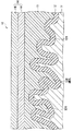
次に、図3を参照して、コンデンサ素子10の詳細な構成について説明する。図3は、図2に示したコンデンサ素子10の断面構成を部分的に拡大して表している。
Next, a detailed configuration of the
コンデンサ素子10では、例えば、図3に示したように、陽極11を覆うように誘電体層12、固体電解質層13および陰極14(副電極層14A,主電極層14B)がこの順に積層されている。このコンデンサ素子10では、陽極11の表面積を増大させることにより高容量化を実現するために、上記したように、その陽極11に拡面化処理(または粗面化処理)が施されており、すなわち陽極11が微細な表面凹凸構造を有している。この陽極11の表面凹凸構造を反映して、その陽極11を覆うように配設されている誘電体層12は微細な凹凸構造を有しており、この微細な凹凸構造を有する誘電体層12を覆うように固体電解質層13および陰極14(副電極層14A,主電極層14B)が配設されている。特に、誘電体層12は、凹凸構造のうちの凹部として複数の細孔12Hを構成しており、固体電解質層13は、誘電体層12により構成された複数の細孔12Hに部分的に入り込んでいる。
In the
図1〜図3に示した電解コンデンサでは、図示しない陽極リードおよび陰極リードを通じてコンデンサ素子10が通電されることにより、そのコンデンサ素子10において電荷が蓄えられる。この際、PTC機能を有する陰極14(主電極層14B)を利用して、短絡時の発熱に起因する電解コンデンサの破壊が防止される。すなわち、例えば、電解コンデンサに過電圧や逆電圧が印加された場合に、誘電体層12が部分的に破損して短絡したことに起因して陽極11と固体電解質層13および陰極14(副電極層14A,主電極層14B)との間に過電流が流れて発熱すると、その短絡時の発熱に基づいて主電極層14Bの温度が上昇することにより抵抗が指数関数的に上昇する結果、コンデンサ素子10中を流れる過電流が抑制されるため、その過電流に起因してコンデンサ素子10が破壊されにくくなる。なお、主電極層14Bの温度が上昇する要因としては、例えば、上記した短絡時の発熱の他に、過電流に起因するジュール熱も含まれる。こののち、主電極層14Bの温度が低下すると、その温度低下に応じて主電極層14Bの抵抗が低下するため、コンデンサ素子10が通電可能な状態に復帰する。
In the electrolytic capacitor shown in FIGS. 1 to 3, electric charge is stored in the
なお、主電極層14BがPTC機能を有する原理は、以下の通りである。すなわち、温度上昇前の段階では、主電極層14Bを構成している膜状高分子中において導電性粒子がチェーン(いわゆる導電パス)を構築しており、そのチェーンが膜状高分子により安定に保持されているため、そのチェーンの存在に基づいて主電極層14Bが低抵抗状態にある。しかしながら、主電極層14Bの温度が上昇すると、膜状高分子の膨張現象に起因してチェーンが切断されるため、主電極層14Bが高抵抗状態になる。もちろん、主電極層14Bの温度が低下すると、膜状高分子の収縮現象に基づいてチェーンが再構築されるため、主電極層14Bが再び低抵抗状態となる。したがって、上記したチェーンの構築・切断・再構築メカニズムを利用して主電極層14Bの抵抗状態が可逆的に変化可能なため、その主電極層14BがPTC機能を有するのである。
The principle that the
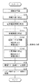
次に、図1〜図4を参照して、本発明の一実施の形態に係る電解コンデンサの製造方法として、図1〜図3に示したコンデンサ素子10を備えた電解コンデンサの製造方法について説明する。図4は、電解コンデンサの製造方法に関する製造工程の流れを説明するためのものである。なお、以下では、電解コンデンサ(コンデンサ素子10)を構成する各構成要素の材質に関しては既に詳細に説明したので、その説明を随時省略するものとする。
Next, with reference to FIGS. 1-4, the manufacturing method of the electrolytic capacitor provided with the capacitor |
電解コンデンサを製造する際には、まず、図1〜図3に示したコンデンサ素子10を形成する。すなわち、まず、陽極11として、例えば、拡面化処理が施された処理済みの弁作用金属箔(例えばアルミニウム箔やチタン箔)、すなわち微細な表面凹凸構造を有する陽極11を準備する(図4;ステップS101)。この陽極11としては、例えば、上記した拡面化処理済みの弁作用金属箔に代えて、タンタルまたはニオブなどの弁作用金属焼結体も使用可能である。なお、陽極11を準備する際には、例えば、上記したように拡面化処理済みの弁作用金属箔を使用する代わりに、未処理の弁作用金属箔を使用し、化学的または電気化学的エッチングを使用して弁作用金属箔に拡面化処理を施すことにより陽極11を形成してもよい。
When manufacturing an electrolytic capacitor, first, the
続いて、陽極11の表層を陽極酸化することにより、その陽極11の周囲を部分的に覆うように酸化皮膜よりなる誘電体層12を形成する(図4;ステップS102)。この誘電体層12としては、例えば、陽極11の形成材料としてアルミニウム箔を使用した場合には、酸化アルミニウムの皮膜により構成されるように誘電体層12を形成可能である。この誘電体層12を形成する際には、例えば、陽極11を化成溶液に浸漬させたのち、その陽極12に電圧を印加することにより陽極酸化反応を進行させるようにする。この化成溶液としては、例えば、ホウ酸アンモニウム、リン酸アンモニウムまたは有機酸アンモニウムなどを含む緩衝溶液を使用し、具体的にはアジピン酸アンモニウム水溶液などを使用する。なお、陽極11に印加する電圧は、例えば、誘電体層12の形成厚さに応じて数V〜数百Vの範囲内で自由に設定可能である。
Subsequently, the surface layer of the
続いて、誘電体層12を覆うように、ドーパントがドープされた導電性高分子を生成することにより、その導電性高分子を含むように固体電解質層13を形成する(図4;ステップS103)。この固体電解質層13を形成する際には、例えば、単量体、ドーパントおよび酸化剤を溶媒に分散させた溶液(単量体溶液)を調製し、その単量体溶液を誘電体層12の表面に塗布したのち、単量体溶液を加熱し、その単量体溶液中の酸化剤を使用して単量体を酸化重合させることにより導電性高分子を生成する。なお、導電性高分子を生成したのちには、例えば、水、アルコール、アセトンまたはヘキサンなどを使用して導電性高分子を洗浄することにより、導電性高分子に含まれている未重合の単量体、導電性高分子にドープされなかった過剰なドーパント、ならびに使用済みの酸化剤などを洗い流して除去するのが好ましい。単量体溶液の加熱温度および加熱時間は、例えば、単量体の反応性(重合性)や酸化剤の反応性(酸化力)等を考慮して適宜設定可能である。
Subsequently, a conductive polymer doped with a dopant is generated so as to cover the
なお、単量体溶液を調整する際には、単量体として、例えば、アニリン、ピロール、チオフェン、フラン、チオフェンビニレン、イソチアナフテン、アセチレン、p−フェニレン、フェニレンビニレン、メトキシビニレン、メトキシフェニレン、フェニレンスルファイド、フェニレンオキシド、アントラセン、ナフタレン、ピレン、アズレン、セレノフェン、テルロフェンおよびこれらの誘導体を含む群のうちの少なくとも1種を使用し、具体的には3,4−エチレンジオキシチオフェンなどを使用する。 In preparing the monomer solution, examples of the monomer include aniline, pyrrole, thiophene, furan, thiophene vinylene, isothianaphthene, acetylene, p-phenylene, phenylene vinylene, methoxy vinylene, methoxy phenylene, Use at least one of the group comprising phenylene sulfide, phenylene oxide, anthracene, naphthalene, pyrene, azulene, selenophene, tellurophene and their derivatives, specifically 3,4-ethylenedioxythiophene, etc. To do.
また、ドーパントとして、例えば、ドナー型またはアクセプター型のいずれのドーパントも使用可能であり、下記の一連の材料を含む群のうちの少なくとも1種を使用する。ドナー型のドーパントとしては、例えば、リチウム(Li)、ナトリウム(Na)またはカリウム(K)などのアルカリ金属や、カルシウム(Ca)などのアルカリ土類金属等が挙げられる。一方、アクセプター型のドーパントとしては、例えば、塩素(Cl2 )、臭素(Br2 )またはヨウ素(I2 )などのハロゲンや、フッ化リン(PF3 )、フッ化ヒ素(AsF5 )またはフッ化ホウ素(BF3 )などのルイス酸や、フッ化水素(HF)、塩化水素(HCl)、硝酸(HNO3 )、硫酸(H2 SO4 )、リン酸(H3 PO4 )または過塩素酸(HClO4 )などのプロトン酸や、アルキルベンゼンスルホン酸(例えばパラトルエンスルホン酸)、アルキルナフタレンスルホン酸またはこれらの塩(例えばパラトルエンスルホン酸ナトリウムまたはアルキルナフタレンスルホン酸ナトリウム)や、塩化鉄(FeCl3 )、過塩素酸鉄(FeOCl2 )、塩化チタン(TiCl4 )または塩化タングステン(WCl3 )などの遷移金属化合物や、塩素イオン(Cl- )、臭素イオン(Br- )、ヨウ素イオン(I- )、過塩素酸イオン(ClO4 -)、フッ化リンイオン(PF3 -)、フッ化ホウ素イオン(BF3 -)またはフッ化ヒ素イオン(AsF3 -)などの電解質アニオン等が挙げられる。 In addition, as the dopant, for example, either a donor-type or acceptor-type dopant can be used, and at least one of a group including the following series of materials is used. Examples of the donor-type dopant include alkali metals such as lithium (Li), sodium (Na), and potassium (K), and alkaline earth metals such as calcium (Ca). On the other hand, examples of acceptor-type dopants include halogens such as chlorine (Cl 2 ), bromine (Br 2 ), and iodine (I 2 ), phosphorus fluoride (PF 3 ), arsenic fluoride (AsF 5 ), and fluorine. Lewis acids such as boron fluoride (BF 3 ), hydrogen fluoride (HF), hydrogen chloride (HCl), nitric acid (HNO 3 ), sulfuric acid (H 2 SO 4 ), phosphoric acid (H 3 PO 4 ) or perchlorine Protic acids such as acids (HClO 4 ), alkylbenzene sulfonic acids (eg, paratoluene sulfonic acid), alkyl naphthalene sulfonic acids or salts thereof (eg, sodium paratoluene sulfonate or sodium alkyl naphthalene sulfonate), iron chloride (FeCl 3), perchlorate (FeOCl 2), a transition such as titanium chloride (TiCl 4) or tungsten chloride (WCl 3) Or group compound, chlorine ion (Cl -), a bromine ion (Br -), iodide ion (I -), perchlorate ion (ClO 4 -), fluoride phosphorus (PF 3 -), boron fluoride ions (BF 3 − ) or electrolyte anions such as arsenic fluoride ion (AsF 3 − ).
さらに、酸化剤として、例えば、ヨウ素または臭素などのハロゲンや、五フッ化ケイ素(SiF5 )などの金属ハロゲン化物や、硫酸などのプロトン酸や、三酸化硫黄(SO3 )などの酸素化合物や、硫酸セリウム(Ce(SO4 )2 )などの硫酸塩や、過硫酸ナトリウム(Na2 S2 O8 )などの過硫酸塩や、過酸化水素(H2 O2 )などの過酸化物や、アルキルベンゼンスルホン酸塩(例えばパラトルエンスルホン酸鉄)などを使用する。 Further, as the oxidizing agent, for example, halogen such as iodine or bromine, metal halide such as silicon pentafluoride (SiF 5 ), protonic acid such as sulfuric acid, oxygen compound such as sulfur trioxide (SO 3 ), , Sulfates such as cerium sulfate (Ce (SO 4 ) 2 ), persulfates such as sodium persulfate (Na 2 S 2 O 8 ), peroxides such as hydrogen peroxide (H 2 O 2 ) Alkylbenzene sulfonate (for example, iron iron p-toluenesulfonate) is used.
なお、溶媒として、例えば、水や、ブタノールなどの有機溶媒等を使用する。 As the solvent, for example, water or an organic solvent such as butanol is used.
上記した酸化重合反応を経て生成される導電性高分子は、例えば、ポリアニリン、ポリピロール、ポリチオフェン、ポリフラン、ポリチオフェンビニレン、ポリイソチアナフテン、ポリアセチレン、ポリ−p−フェニレン、ポリフェニレンビニレン、ポリメトキシビニレン、ポリメトキシフェニレン、ポリフェニレンスルファイド、ポリフェニレンオキシド、ポリアントラセン、ポリナフタレン、ポリピレン、ポリアズレン、ポリセレノフェン、ポリテルロフェンおよびこれらの誘導体を含む群のうちの少なくとも1種であり、具体的にはポリエチレンジオキシチオフェンである。この導電性高分子としては、例えば、高分子骨格中に一次元的連鎖を有し、かつ電子供与性機能または電子受容性機能(いわゆるドーパミン機能)を有する共役系高分子が好ましい。 The conductive polymer produced through the above oxidative polymerization reaction is, for example, polyaniline, polypyrrole, polythiophene, polyfuran, polythiophene vinylene, polyisothianaphthene, polyacetylene, poly-p-phenylene, polyphenylene vinylene, polymethoxy vinylene, poly At least one member selected from the group comprising methoxyphenylene, polyphenylene sulfide, polyphenylene oxide, polyanthracene, polynaphthalene, polypyrene, polyazulene, polyselenophene, polytellurophene and their derivatives, specifically polyethylenedioxy Thiophene. As the conductive polymer, for example, a conjugated polymer having a one-dimensional chain in the polymer skeleton and having an electron donating function or an electron accepting function (so-called dopamine function) is preferable.
引き続き、電解コンデンサの製造工程について説明する。陽極11、誘電体層12および固体電解質層13がこの順に積層された積層構造を形成したのち、その固体電解質層13を覆うように、PTC機能を有する陰極14を形成する(図4;ステップS104)。この陰極14を形成する際には、固体電解質層13の表面に液状材料を供給して膜化することにより、PTC機能を有するように陰極14を形成する。
Next, the manufacturing process of the electrolytic capacitor will be described. After forming a laminated structure in which the
この陰極14の形成手順は、例えば、以下の通りである。すなわち、まず、固体電解質層13の表面に液状材料としてカーボンペーストを供給したのち、そのカーボンペーストを乾燥して膜化することにより副電極層14Aを形成する(ステップS1041)。このカーボンペーストの供給方法としては、例えば、塗布法(例えばスプレー法、ローラ法またはスピンコート法)、浸漬法(いわゆるディップ法)、あるいは印刷法などを使用可能である。続いて、液状高分子中に導電性粒子を分散させることにより、PTC機能を確保するための液状材料として金属ペーストを準備する(ステップS1042)。この金属ペーストを準備する際には、液状高分子として、例えば、エポキシ樹脂などの熱硬化性高分子およびPVDFなどの可溶性熱可塑性高分子を含む群のうちの少なくとも1種を使用し、導電性粒子として、例えば、金属粒子および導電性セラミック粒子のうちの少なくとも1種を使用する。この金属粒子としては、例えば、ニッケル(Ni)、銅(Cu)、アルミニウム(Al)、タングステン(W)、モリブデン(Mo)、亜鉛(Zn)、コバルト(Co)、白金(Pt)、金(Au)および銀(Ag)などが挙げられ、一方、導電性セラミック粒子としては、例えば、炭化タングステン(WC)、窒化チタン(TiN)、窒化ジルコニウム(ZrN)、炭化チタン(TiC)、ホウ化チタン(TiB2 )、ケイ化モリブデン(MoSi2 )およびホウ化タンタル(TaB2 )などが挙げられる。特に、導電性粒子として金属粒子を使用する場合には、例えば、フィラメント状の金属粒子を使用するのが好ましい。最後に、副電極層14Aの表面に金属ペーストを供給して膜化することにより、その液状高分子が膜化した膜状高分子と、その膜状高分子中に保持された導電性粒子とを含むように、PTC機能を有する主電極層14Bを形成する(ステップS1043)。なお、金属ペーストの供給方法は、例えば、副電極層14Aを形成する場合におけるカーボンペーストの供給方法と同様である。これにより、副電極層14Aおよび主電極層14Bを含む2層構造を有するように陰極14が形成される。この結果、陽極11、誘電体層12、固体電解質層13および陰極14(副電極層14A,主電極層14B)がこの順に積層された積層構造を有するコンデンサ素子10が完成する。
The formation procedure of the
コンデンサ素子10を形成したのち、このコンデンサ素子10を使用して電解コンデンサを組み立てる。すなわち、例えば、コンデンサ素子10のうちの陽極11に陽極リードを接続させると共に、陰極14に陰極リードを接続させたのち(図4;ステップS105)、陽極リードおよび陰極リードの双方が部分的に露出するようにコンデンサ素子10の周囲をモールド樹脂で被覆する(図4;ステップS106)。これにより、コンデンサ素子10に陽極リードおよび陰極リードが接続され、それらの陽極リードおよび陰極リードの双方が部分的に露出するようにコンデンサ素子10がモールド樹脂により周囲を覆われた構造を有する電解コンデンサが完成する。なお、コンデンサ素子10に陽極リードおよび陰極リードを接続させる際には、例えば、溶接処理またはかしめ加工を使用して直接的に接続させるようにしてもよいし、あるいは導電性接着剤を使用して間接的に接続させるようにしてもよい。
After the
本実施の形態に係る電解コンデンサの製造方法では、固体電解質13上にPTC機能を有する2層構造(副電極層14A,主電極層14B)の陰極14を形成する際に、固体電解質層13の表面にカーボンペーストを供給して膜化することにより副電極層14Aを形成したのち、その副電極層14Aの表面に金属ペースト(液状高分子,導電性粒子)を供給して膜化することにより主電極層14B(膜状高分子,導電性粒子)を形成するようにしたので、上記したPTC機能の原理に基づき、陰極14のうちの主電極層14BにPTC機能が付与される。従来の電解コンデンサの製造方法では、電解コンデンサにPTC機能を付与するためにコンデンサ素子にPTCサーミスタを熱圧着させているため、その熱圧着時に生じる力学的要因(コンデンサ素子に加わる過度な外力)に起因して誘電体層が製造途中において著しく破損しやすい。これに対して、本実施の形態に係る電解コンデンサの製造方法では、従来の電解コンデンサの製造方法とは異なり、誘電体層12に過度な外力が加わらないため、その誘電体層12が製造途中において力学的要因に起因して破損しにくくなる。これにより、PTC機能を利用して短絡時の発熱に起因する電解コンデンサの破壊を防止しつつ、その電解コンデンサの製造歩留まりを高めることにより生産性を確保することが可能となる。したがって、PTC機能を有する電解コンデンサが製造途中において力学的に破壊されることを防止することにより、そのPTC機能を有する電解コンデンサを可能な限り安定に製造することができる。
In the electrolytic capacitor manufacturing method according to the present embodiment, when the
なお、本実施の形態に係る電解コンデンサの製造方法と従来の電解コンデンサの製造方法との差異に関して確認までに説明しておくと、本実施の形態では、主電極層14Bを形成する際に副電極層14Aの表面に金属ペーストが供給されるため、誘電体層12に外力が全く加わらないわけではなく、その金属ペーストの供給処理に基づく外力が誘電体層12に加わることとなるが、言うまでもなく、その金属ペーストの供給処理に基づく外力は圧着処理に基づく外力よりも格段に小さくなり、すなわち電解コンデンサの製造途中において誘電体層12を力学的に破損させる程度ではないため、当然ながら、金属ペーストの供給処理に基づく外力に起因して誘電体層12が破損する可能性は、圧着処理に基づく外力に起因して誘電体層が破損する可能性よりも極めて小さくなる。
It should be noted that the difference between the electrolytic capacitor manufacturing method according to the present embodiment and the conventional electrolytic capacitor manufacturing method will be described before confirmation. In the present embodiment, when the
特に、本実施の形態では、上記したように、陰極14、具体的には陰極14の一部を構成する主電極層14BがPTC機能を有するようにしたので、コンデンサ素子にそのコンデンサ素子以外の構成部品としてPTCサーミスタを外付けする従来の電解コンデンサの製造方法とは異なり、コンデンサ素子10のもともとの構成部品である陰極14にPTC機能が付与される。この場合には、従来の場合とは異なり、電解コンデンサの構成部品を増やさずにPTC機能が確保されるため、電解コンデンサの構成が複雑化することが防止されると共に、コンデンサ素子10に新たな構成部品を外付けする必要がないため、電解コンデンサの製造工程数が増加することが防止される。したがって、PTC機能を確保するための液状材料(液状高分子,導電性粒子)を使用して主電極層14Bを形成する変更点だけで、PTC機能を有していない現行の電解コンデンサの製造方法をそのまま流用して電解コンデンサを製造可能なため、PTC機能を有する電解コンデンサを可能な限り容易に製造することができる。
In particular, in the present embodiment, as described above, the
また、上記した他、本実施の形態に係る電解コンデンサでは、主電極層14BのPTC機能に基づき、短絡時の発熱に起因して破壊されにくくなるため、PTC機能を利用して短絡時の発熱に起因する破壊を可能な限り防止することができる。
In addition to the above, in the electrolytic capacitor according to the present embodiment, the PTC function of the
なお、本実施の形態では、陰極14のうちの主電極層14BのみがPTC機能を有するようにしたが、必ずしもこれに限られるものではなく、例えば、主電極層14Bに代えて副電極層14AのみがPTC機能を有するようにしてもよいし、あるいは副電極層14Aおよび主電極層14Bの双方がPTC機能を有するようにしてもよい。主電極層14Bに代えて副電極層14AのみがPTC機能を有するようにする場合には、例えば、副電極層14Aの形成材料(液状材料)として液状高分子および導電性粒子を含むカーボンペーストを使用し、上記実施の形態において主電極層14Bを形成した場合と同様の工程を経ることにより膜状高分子および導電性粒子を含むように副電極層14Aを形成することにより、その副電極層14AにPTC機能を付与することが可能である。この場合には、例えば、液状高分子として上記実施の形態において説明した場合と同様の熱硬化性高分子および可溶性熱可塑性高分子のうちの少なくとも1種を使用し、導電性粒子としてカーボンブラック(CB;Carbon Black)などのカーボン粒子を使用すると共に、主電極層14の形成材料(液状材料)としてPTC機能を確保し得ない一般的な金属ペースト(例えば銀ペースト等)を使用する。なお、副電極層14Aおよび主電極層14Bの双方がPTC機能を有するようにする場合には、例えば、上記したPTC機能を有する副電極層14AとPTC機能を有する主電極層14Bとを組み合わせればよい。これらの場合においても、陰極14にPTC機能が付与されるため、上記実施の形態と同様の効果を得ることができる。
In the present embodiment, only the
また、本実施の形態では、陰極14が2層構造(副電極層14A,主電極層14B)を有するようにしたが、必ずしもこれに限られるものではなく、その陰極14の積層構造数は2層以上の範囲で自由に変更可能である。この場合においても、陰極14が電極として機能し得るだけの抵抗特性を有すると共にPTC機能を確保し得る限り、上記実施の形態と同様の効果を得ることができる。もちろん、この場合においても、例えば、陰極14の積層構造中の一部の層のみがPTC機能を有するようにしてもよいし、あるいは積層構造中の全ての層がPTC機能を有するようにしてもよい。
In the present embodiment, the
また、本実施の形態では、陰極14が積層構造(副電極層14A,主電極層14B)を有するようにしたが、必ずしもこれに限られるものではなく、例えば、図5に示したように、陰極14が単層構造を有するようにしてもよい。この場合には、上記実施の形態において説明したPTC機能を有する主電極層14Bに相当する構成となるように陰極14を構成してもよいし、あるいは上記変形例において説明したPTC機能を有する副電極層14Aに相当する構成となるように陰極14を構成してもよい。ただし、例えば、PTC機能を有する副電極層14Aに含まれる導電性粒子(例えばカーボン粒子)とPTC機能を有する主電極層14Bに含まれる導電性粒子(例えば金属粒子または導電性セラミック粒子)との間で抵抗特性を比較すると、導電性粒子に基づく抵抗値はカーボン粒子よりも金属粒子または導電性セラミック粒子において低くなるため、陰極14がPTC機能と共に電極機能を担うことを考慮すれば、PTC機能を有する主電極層14Aに相当する構成となるように陰極14を構成するのが好ましい。この場合においても、上記実施の形態と同様の効果を得ることができる。なお、図5に示したコンデンサ素子10に関する上記以外の構成的特徴は、例えば、図2に示した場合と同様である。
In the present embodiment, the
次に、本発明の具体的な実施例について説明する。 Next, specific examples of the present invention will be described.
上記実施の形態において説明した電解コンデンサの製造方法を使用して、電解コンデンサを製造した。すなわち、まず、陽極として処理済み(拡面化処理済み)のアルミニウム箔を準備したのち、化成溶液中においてアルミニウム箔に電圧(=23V)を印加し、陽極酸化反応を進行させて酸化アルミニウム皮膜を形成することにより、誘電体層を形成した。この誘電体層の形成後、アジピン酸アンモニウム水溶液中で容量を測定したところ、理論容量は約100μFであった。続いて、単量体、ドーパントおよび酸化剤を溶媒に分散させた単量体溶液を準備し、誘電体層を形成済みの陽極を単量体溶液に30秒間に渡って浸漬させることにより、その誘電体層の表面に単量体溶液を付着させたのち、陽極を0.5mm/秒で引き上げて室温乾燥させた。続いて、単量体溶液に浸漬済みの陽極を乾燥器に投入して加熱し、その単量体溶液に含まれている酸化剤を使用して単量体を酸化重合させることにより、ドーパントがドープされた導電性高分子を含むように固体電解質層を形成した。続いて、固体電解質層の表面にカーボンペーストを塗布して乾燥させることにより副電極層を形成したのち、その副電極層の表面に金属ペーストを塗布して乾燥させることにより主電極層を形成し、これらの副電極層および主電極層を含む2層構造を有するように陰極を形成した。これにより、陽極、誘電体層、固体電解質層および陰極(副電極層,主電極層)がこの順に積層された積層構造を有するコンデンサ素子が形成された。最後に、導電性接着剤(銀接着剤)を使用してコンデンサ素子に銅製の陽極リードおよび陰極リードを接続させたのち、モールド樹脂としてエポキシ樹脂で陽極リードおよび陰極リードが部分的に露出するようにコンデンサ素子の周囲を覆うことにより、電解コンデンサが完成した。 An electrolytic capacitor was manufactured using the electrolytic capacitor manufacturing method described in the above embodiment. That is, first, a treated (surface-enhanced) aluminum foil is prepared as an anode, and then a voltage (= 23 V) is applied to the aluminum foil in the chemical conversion solution to advance the anodic oxidation reaction to form an aluminum oxide film. By forming, a dielectric layer was formed. After the formation of this dielectric layer, the capacity was measured in an aqueous solution of ammonium adipate. The theoretical capacity was about 100 μF. Subsequently, a monomer solution in which a monomer, a dopant and an oxidant are dispersed in a solvent is prepared, and the anode on which the dielectric layer has been formed is immersed in the monomer solution for 30 seconds. After the monomer solution was attached to the surface of the dielectric layer, the anode was pulled up at 0.5 mm / second and dried at room temperature. Subsequently, the anode immersed in the monomer solution is put into a dryer and heated, and the dopant is oxidized by oxidative polymerization of the monomer using the oxidizing agent contained in the monomer solution. A solid electrolyte layer was formed to include the doped conductive polymer. Subsequently, after forming a sub-electrode layer by applying and drying a carbon paste on the surface of the solid electrolyte layer, a main electrode layer is formed by applying and drying a metal paste on the surface of the sub-electrode layer. The cathode was formed so as to have a two-layer structure including these sub-electrode layers and main electrode layer. As a result, a capacitor element having a laminated structure in which the anode, the dielectric layer, the solid electrolyte layer, and the cathode (sub-electrode layer, main electrode layer) were laminated in this order was formed. Finally, after connecting the copper anode lead and cathode lead to the capacitor element using a conductive adhesive (silver adhesive), the anode lead and cathode lead are partially exposed with epoxy resin as the mold resin. The electrolytic capacitor was completed by covering the periphery of the capacitor element.
なお、固体電解質層の形成手順は、以下の通りである。すなわち、まず、単量体として3,4−エチレンジオキシチオフェン(バイエル株式会社製Baytron M (商品名))、ならびにドーパント兼酸化剤としてパラトルエンスルホン酸鉄(III)50%ブタノール溶液(バイエル株式会社製Baytron C (商品名))を氷水で十分に冷却したのち、これらの単量体およびドーパント兼酸化剤をそれぞれ0.867g,10.4g秤量し、氷水で冷却しながらマグネチックスターラーで混合・攪拌することにより単量体溶液を調製した。続いて、誘電体層を形成済みの陽極を上記した浸漬条件で単量体溶液に浸漬させることにより、その誘電体層の表面に単量体溶液を付着させた。続いて、単量体溶液が付着された誘電体層を室温下において1時間程度放置したのち、その単量体溶液を加熱して単量体を酸化重合させることにより、誘電体層を覆うように導電性高分子としてポリエチレンジオキシチオフェンを生成した。この際、加熱条件は加熱温度=100℃、加熱時間=15分間とした。最後に、蒸留水を使用して導電性高分子を十分に洗浄することにより、未重合の単量体、過剰なドーパント、ならびに使用済みの酸化剤などを洗い流したのち、その導電性高分子を乾燥させた。なお、導電性高分子を形成する際には、上記した導電性高分子の生成手順を3回繰り返し、特に、酸化重合反応の完了時ごとに蒸留水やエタノールを使用して導電性高分子を洗浄することにより、未重合の単量体、余剰なドーパントならびに使用済みの酸化剤を随時除去した。これにより、導電性高分子を含む固体電解質層が形成された。 The procedure for forming the solid electrolyte layer is as follows. First, 3,4-ethylenedioxythiophene as a monomer (Baytron M (trade name) manufactured by Bayer Co., Ltd.) and 50% butanol solution of iron (III) paratoluenesulfonate as a dopant and oxidizing agent (Bayer shares) After sufficiently cooling the company's Baytron C (trade name) with ice water, weigh out 0.867 g and 10.4 g of these monomers and dopant / oxidizer, and mix them with a magnetic stirrer while cooling with ice water. -A monomer solution was prepared by stirring. Subsequently, the monomer solution was attached to the surface of the dielectric layer by immersing the anode on which the dielectric layer had been formed in the monomer solution under the immersion conditions described above. Subsequently, the dielectric layer to which the monomer solution is attached is allowed to stand at room temperature for about 1 hour, and then the monomer solution is heated to oxidatively polymerize the monomer so as to cover the dielectric layer. Polyethylenedioxythiophene was produced as a conductive polymer. At this time, the heating conditions were heating temperature = 100 ° C. and heating time = 15 minutes. Finally, the conductive polymer is thoroughly washed with distilled water to wash away unpolymerized monomers, excess dopant, used oxidant, etc., and then remove the conductive polymer. Dried. When forming the conductive polymer, the above-mentioned procedure for generating the conductive polymer is repeated three times. In particular, the conductive polymer is prepared using distilled water or ethanol every time the oxidative polymerization reaction is completed. By washing, unpolymerized monomer, excess dopant and used oxidizing agent were removed as needed. Thereby, a solid electrolyte layer containing a conductive polymer was formed.
上記した電解コンデンサの製造方法を使用して、PTC機能を有する陰極(副電極層,主電極層)の構成を以下のように変化させながら本発明の電解コンデンサ(実施例1〜6)を製造したのち、その電解コンデンサの諸特性を調べた。なお、本発明の電解コンデンサの諸特性を調べる際には、その性能を比較評価するために、陰極の構成を以下のように変化させながら比較例の電解コンデンサ(比較例1〜3)を製造し、その電解コンデンサの諸特性も併せて調べた。 Using the electrolytic capacitor manufacturing method described above, the electrolytic capacitor (Examples 1 to 6) of the present invention is manufactured while changing the configuration of the cathode (sub electrode layer, main electrode layer) having the PTC function as follows. After that, the characteristics of the electrolytic capacitor were investigated. When investigating various characteristics of the electrolytic capacitor of the present invention, comparative electrolytic capacitors (Comparative Examples 1 to 3) were manufactured while changing the configuration of the cathode as follows in order to compare and evaluate the performance. The characteristics of the electrolytic capacitor were also investigated.
(実施例1)
以下の手順を経ることにより、主電極層のみがPTC機能を有するように陰極を形成した。すなわち、副電極層の形成材料(カーボンペースト)として田中貴金属工業株式会社製のカーボンブラック(CB)ペースト TC−8263を使用し、固体電解質層の表面にカーボンペーストを塗布したのちに125℃で乾燥させることにより副電極層を形成した。また、主電極層の形成材料(金属ペースト)として、液状高分子(膜状高分子)として熱硬化性高分子、具体的には大日本インキ化学工業株式会社製のエポキシ樹脂 EPICLON850(エポキシ当量=190g/eq)と旭電化工業株式会社製のエポキシ樹脂 EP4005(エポキシ当量=510g/eq)との混合物(エポキシ樹脂α;配合重量比(EPICLON850:EP4005)=75:25)を使用すると共に、導電性粒子としてINCO Limited社製のフィラメント状ニッケルパウダ Type255(Niα;平均粒径=2.2μm〜2.8μm,見かけ密度=0.50g/cm3 〜0.65g/cm3 ,比表面積=0.68m2 /g,添加重量比(液状高分子:導電性粒子)=40:60)を使用し、副電極層の表面に金属ペーストを塗布したのちに窒素雰囲気下において130℃で加熱硬化させることにより、0.2mmの厚さとなるように主電極層を形成した。なお、金属ペーストとしては、上記した液状高分子および導電性粒子と共に、硬化補助剤として、大日本インキ化学工業株式会社製の硬化剤 B570(酸無水物当量=168g/eq,液状高分子に対して当量比=1:1)と、味の素ファインテクノ株式会社製の硬化促進剤 PN−40J(添加量=液状高分子の重量に対して1重量%)とを含むものを使用した。
(Example 1)
Through the following procedure, the cathode was formed so that only the main electrode layer had the PTC function. That is, carbon black (CB) paste TC-8263 manufactured by Tanaka Kikinzoku Kogyo Co., Ltd. was used as the material for forming the sub-electrode layer (carbon paste), and the carbon paste was applied to the surface of the solid electrolyte layer and then dried at 125 ° C. As a result, a sub-electrode layer was formed. In addition, as a material for forming the main electrode layer (metal paste), a thermosetting polymer as a liquid polymer (film polymer), specifically, an epoxy resin EPICLON850 (Epoxy equivalent = 190 g / eq) and epoxy resin EP4005 (epoxy equivalent = 510 g / eq) manufactured by Asahi Denka Kogyo Co., Ltd. (epoxy resin α; blending weight ratio (EPICLON 850: EP4005) = 75: 25) Filamentous nickel powder Type 255 (Niα; average particle size = 2.2 μm to 2.8 μm, apparent density = 0.50 g / cm 3 to 0.65 g / cm 3 , specific surface area = 0. 68m 2 / g, the addition weight ratio (liquid polymer: conductive particles) = 40: 60) using a metal on the surface of the auxiliary electrode layer Bae By heat curing at 130 ° C. under a nitrogen atmosphere was coated strike to form a main electrode layer to a thickness of 0.2 mm. In addition, as a metal paste, the curing agent B570 (acid anhydride equivalent = 168 g / eq, manufactured by Dainippon Ink & Chemicals, Inc.) as a curing auxiliary agent together with the above-described liquid polymer and conductive particles. Equivalent ratio = 1: 1) and a curing accelerator PN-40J manufactured by Ajinomoto Fine Techno Co., Ltd. (addition amount = 1 wt% based on the weight of the liquid polymer) was used.
(実施例2)
導電性粒子としてNovamet Specialty Products Corporation社製の銀被覆ニッケルフレーク(Niβ;銀被覆率=15%,見かけ密度=2.4g/cc,添加重量比(液状高分子:導電性粒子)=45:55)を使用した点を除き、実施例1と同様の手順を経ることにより陰極を形成した。
(Example 2)
Silver-coated nickel flakes manufactured by Novamet Specialty Products Corporation (Niβ; silver coverage = 15%, apparent density = 2.4 g / cc, added weight ratio (liquid polymer: conductive particles) = 45: 55 The cathode was formed by going through the same procedure as in Example 1 except that.
(実施例3)
主電極層の形成材料(金属ペースト)として、液状高分子(膜状高分子)として可溶性熱可塑性高分子、具体的にはアセトンおよびトルエンの混合溶媒に溶解させたAtofina Chemicals 社製のPVDF Kynar7201(融点=122℃〜126℃,比重=1.88)を使用すると共に、導電性粒子として日本新金属株式会社製のWC(炭化タングステン) WC−F(粒径=0.62μm,添加容量比(液状高分子:導電性粒子)=70:30)を使用し、ボールミルで液状高分子中において導電性粒子を攪拌することにより調製した金属ペーストを副電極層の表面に塗布したのちに100℃で真空乾燥させることにより、0.2μmの厚さとなるように主電極層を形成した点を除き、実施例1と同様の手順を経ることにより陰極を形成した。
(Example 3)
As a main electrode layer forming material (metal paste), PVDF Kynar 7201 (manufactured by Atofina Chemicals) dissolved in a soluble thermoplastic polymer as a liquid polymer (film polymer), specifically, a mixed solvent of acetone and toluene. Melting point = 122 ° C.-126 ° C., specific gravity = 1.88) and WC (tungsten carbide) WC-F (particle size = 0.62 μm, additive capacity ratio (made by Nippon Shin Metals Co., Ltd.) as conductive particles Liquid polymer: conductive particles) = 70: 30), and a metal paste prepared by stirring the conductive particles in the liquid polymer with a ball mill was applied to the surface of the sub-electrode layer at 100 ° C. A cathode was formed by performing the same procedure as in Example 1 except that the main electrode layer was formed to have a thickness of 0.2 μm by vacuum drying.
(実施例4)
以下の手順を経ることにより、副電極層のみがPTC機能を有するように陰極を形成した。すなわち、副電極層の形成材料(カーボンペースト)として、液状高分子(膜状高分子)として熱硬化性高分子、具体的には実施例1で使用したエポキシ樹脂α(硬化補助剤(硬化剤,硬化促進剤)を含む)を使用すると共に、導電性粒子として東海カーボン株式会社製のカーボンブラック(CB) #4500 トーカブラック(粒径=40nm,DBP給油量=168cc/100g,比表面積=58m2 /g,添加重量比(液状高分子:導電性粒子)=67:33)を使用し、液状高分子および導電性粒子を攪拌混合した混合物を固体電解質層の表面に塗布したのちに窒素雰囲気下において130℃で加熱硬化させることにより副電極層を形成した。また、主電極層の形成材料(金属ペースト)として田中貴金属工業株式会社製の銀ペースト NH1429Nを使用し、副電極層の表面に金属ペーストを塗布したのちに乾燥させることにより主電極層を形成した。
Example 4
Through the following procedure, the cathode was formed so that only the sub-electrode layer had the PTC function. That is, as a material for forming the sub-electrode layer (carbon paste), a thermosetting polymer as a liquid polymer (film-like polymer), specifically, the epoxy resin α (curing auxiliary agent (curing agent) used in Example 1 Carbon black (CB) # 4500 Toka Black (particle size = 40 nm, DBP oil supply = 168 cc / 100 g, specific surface area = 58 m, manufactured by Tokai Carbon Co., Ltd. as conductive particles. 2 / g, addition weight ratio (liquid polymer: conductive particles) = 67: 33), a mixture obtained by stirring and mixing the liquid polymer and the conductive particles is applied to the surface of the solid electrolyte layer, and then a nitrogen atmosphere A sub-electrode layer was formed by heating and curing at 130 ° C. below. Further, a silver paste NH1429N manufactured by Tanaka Kikinzoku Kogyo Co., Ltd. was used as a material for forming the main electrode layer (metal paste), and the main electrode layer was formed by applying the metal paste to the surface of the sub-electrode layer and drying it. .
(実施例5)
液状高分子(膜状高分子)として熱硬化性高分子、具体的には日本化薬株式会社製のエポキシ樹脂 AK−601(エポキシ樹脂β;エポキシ当量=153g/eq)を使用した点を除き、実施例4と同様の手順を経ることにより陰極を形成した。
(Example 5)
Except for using a thermosetting polymer as a liquid polymer (film polymer), specifically, an epoxy resin AK-601 (epoxy resin β; epoxy equivalent = 153 g / eq) manufactured by Nippon Kayaku Co., Ltd. The cathode was formed through the same procedure as in Example 4.
(実施例6)
副電極層の形成材料(カーボンペースト)として、液状高分子(膜状高分子)として実施例3で使用したPVDF(アセトンおよびトルエンの混合溶媒に溶解させたPVDF)を使用すると共に、導電性粒子として実施例4で使用したカーボンブラックを使用し、ボールミルで液状高分子中において導電性粒子を攪拌することにより調製したカーボンペーストを固体電解質層の表面に塗布したのちに100℃で真空乾燥させることにより副電極層を形成した点を除き、実施例4と同様の手順を経ることにより陰極を形成した。
(Example 6)
As a material for forming the sub-electrode layer (carbon paste), PVDF used in Example 3 (PVDF dissolved in a mixed solvent of acetone and toluene) is used as a liquid polymer (film polymer), and conductive particles The carbon paste used in Example 4 was used, and the carbon paste prepared by stirring the conductive particles in the liquid polymer with a ball mill was applied to the surface of the solid electrolyte layer and then vacuum-dried at 100 ° C. A cathode was formed by following the same procedure as in Example 4 except that the sub-electrode layer was formed by the above.
(比較例1)
主電極層の形成材料(金属ペースト)として実施例4で使用した銀ペースト(PTC機能無)を使用し、副電極層の表面に金属ペーストを塗布したのちに乾燥させることにより主電極層を形成すると共に、PTC機能を有しないようにした点を除き、実施例1と同様の手順を経ることにより陰極を形成した。
(Comparative Example 1)
The silver paste (no PTC function) used in Example 4 is used as the main electrode layer forming material (metal paste), and the main electrode layer is formed by applying the metal paste to the surface of the sub electrode layer and drying it. In addition, a cathode was formed by following the same procedure as in Example 1 except that the PTC function was not provided.
(比較例2)
主電極層の形成材料として金属ペーストを使用せず、副電極層に熱可塑性の導電性高分子シートを主電極層として熱圧着した点を除き、実施例1と同様の手順を経ることにより陰極を形成した。なお、導電性高分子シートを作製する際には、不溶性熱可塑性高分子、具体的には日本ポリエチレン株式会社製のHDPE(High Dnsity Polyethylene;高密度ポリエチレン) HY540(融点=135℃,比重=0.961)を使用すると共に、導電性粒子としてINCO Limited社製のフィラメント状ニッケルパウダ Type210(平均粒径=0.5μm〜1.0μm,見かけ密度=0.80g/cm3 ,比表面積=1.50m2 /g〜2.50m2 /g,添加重量比(高分子:導電性粒子)=65:35)を使用し、150℃の混練ミル中で高分子および導電性粒子を加熱溶融して混練させたのち、その混練物を熱プレスでシート状に成形した。この導電性高分子シートを副電極層に熱圧着する際には、その導電性高分子シートを副電極層に150℃で熱プレスした。
(Comparative Example 2)
By using the same procedure as in Example 1 except that a metal paste is not used as a material for forming the main electrode layer, and a thermoplastic conductive polymer sheet is thermocompression bonded to the sub electrode layer as the main electrode layer, the cathode is obtained. Formed. In preparing the conductive polymer sheet, an insoluble thermoplastic polymer, specifically, HDPE (High Dnsity Polyethylene) HY540 (melting point = 135 ° C., specific gravity = 0) manufactured by Nippon Polyethylene Co., Ltd. 961) and filamentous nickel powder Type 210 manufactured by INCO Limited (average particle size = 0.5 μm to 1.0 μm, apparent density = 0.80 g / cm 3 , specific surface area = 1.961). 50m 2 /g~2.50m 2 / g, the addition weight ratio (polymer: conductive particles) = 65: 35) using, by heating and melting the polymer and conductive particles in a kneader mill 0.99 ° C. After kneading, the kneaded product was formed into a sheet by a hot press. When this conductive polymer sheet was thermocompression bonded to the sub-electrode layer, the conductive polymer sheet was hot-pressed at 150 ° C. on the sub-electrode layer.
(比較例3)
副電極層の形成材料としてカーボンペーストを使用せず、固体電解質層に熱可塑性の導電性高分子シートを副電極層として熱圧着した点を除き、実施例4と同様の手順を経ることにより陰極を形成した。なお、高分子シートを作製する際には、不溶性熱可塑性高分子、具体的には比較例2で使用したHDPEを使用すると共に、導電性粒子として実施例4で使用したカーボンブラックを使用し、150℃の混練ミル中で高分子および導電性粒子を加熱溶融して混練させたのち、その混練物を熱プレスでシート状に成形した。また、高分子シートを副電極層に熱圧着する際には、その高分子シートを副電極層に150℃で熱プレスした。
(Comparative Example 3)
By using the same procedure as in Example 4 except that carbon paste is not used as the material for forming the subelectrode layer, and a thermoplastic conductive polymer sheet is thermocompression bonded to the solid electrolyte layer as the subelectrode layer, the cathode is obtained. Formed. In preparing the polymer sheet, an insoluble thermoplastic polymer, specifically, HDPE used in Comparative Example 2 was used, and carbon black used in Example 4 was used as the conductive particles. After the polymer and conductive particles were heated and melted and kneaded in a kneading mill at 150 ° C., the kneaded product was formed into a sheet by hot pressing. Further, when the polymer sheet was thermocompression bonded to the sub electrode layer, the polymer sheet was hot pressed at 150 ° C. to the sub electrode layer.
これらの実施例1〜6および比較例1〜3の電解コンデンサの諸特性を調べたところ、表1および表2に示した結果が得られた。 When the characteristics of the electrolytic capacitors of Examples 1 to 6 and Comparative Examples 1 to 3 were examined, the results shown in Table 1 and Table 2 were obtained.
まず、実施例1〜3および比較例1,2の電解コンデンサの諸特性を調べたところ、表1に示した結果が得られた。表1は電解コンデンサの諸特性を表しており、その諸特性として「ESR(Equivalent Series Resistance;等価直列抵抗,mΩ)」、「漏れ電流(μA)」および「逆電圧試験」を示している。「ESR」としては、インピーダンスアナライザを使用して測定した各電解コンデンサの100kHzのESR値を示している。「漏れ電流」としては、各電解コンデンサに電圧(=6.3V)を5分間に渡って印加したのちに測定した漏れ電流値を示している。「逆電圧試験」としては、各電解コンデンサに逆電圧(=60V)を印加した際に不具合(例えば発火または発煙等)が観察されたものを「NG」と示し、不具合が観察されなかったものを「OK」と示している。なお、表1には、参考までに、副電極層および主電極層の材料構成(液状高分子(膜状高分子),導電性粒子)と共に、PTC機能の有無を併せて示している。 First, various characteristics of the electrolytic capacitors of Examples 1 to 3 and Comparative Examples 1 and 2 were examined. The results shown in Table 1 were obtained. Table 1 shows various characteristics of the electrolytic capacitor. As the characteristics, “ESR (Equivalent Series Resistance)”, “Leakage Current (μA)”, and “Reverse Voltage Test” are shown. “ESR” indicates the 100 kHz ESR value of each electrolytic capacitor measured using an impedance analyzer. “Leakage current” indicates a leakage current value measured after applying a voltage (= 6.3 V) to each electrolytic capacitor for 5 minutes. In the “reverse voltage test”, when a reverse voltage (= 60 V) was applied to each electrolytic capacitor, a failure (eg, ignition or smoke) was observed as “NG” and no failure was observed. Is indicated as “OK”. For reference, Table 1 also shows the presence / absence of the PTC function together with the material configuration (liquid polymer (film polymer), conductive particles) of the sub-electrode layer and the main electrode layer.
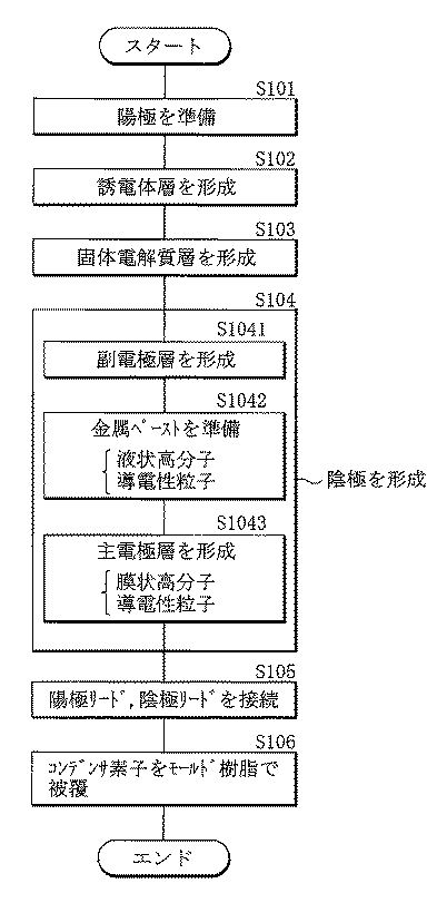
表1に示した結果から判るように、電解コンデンサの実使用上の諸特性として、ESRが100mΩ以下、漏れ電流が10.0μA以下、ならびに逆電圧試験がOKである条件(適性条件)が必要であるとすると、実施例1〜3の電解コンデンサでは、ESR、漏れ電流および逆電圧試験の全てが適性条件を満たした。すなわち、実施例1〜3の電解コンデンサでは、(1)カーボンペーストおよび金属ペーストを塗布して膜化することにより陰極(副電極層,主電極層)を形成しているため、固体電解質層と陰極との間の接触抵抗が低下することに基づいてESRが小さくなり、(2)主電極層を副電極層に熱圧着させていないことにより陰極の形成時に誘電体層に過度な外力が加わらないため、その誘電体層が製造途中において力学的要因に起因して破損しないことに基づいて漏れ電流が小さくなり、(3)逆電圧を印加した際に瞬間的に過電流が流れたが、主電極層のPTC機能を利用して陰極が高抵抗化することにより過電流が抑制されたため、発火または発煙等が生じなかった。これに対して、比較例1,2の電解コンデンサでは、ESR、漏れ電流および逆電圧試験の一部が適性条件を満たさなかった。具体的には、比較例1の電解コンデンサでは、ESRおよび漏れ電流の双方が適性条件を満たした一方で逆電圧試験が適性条件を満たさず、比較例2の電解コンデンサでは、ESRおよび漏れ電流が適性条件を満たさなかった一方で逆電圧試験が適性条件を満たした。すなわち、比較例1の電解コンデンサでは、カーボンペーストおよび金属ペーストを塗布することにより陰極を形成していると共に、主電極層を副電極層に熱圧着させていないため、実施例1〜3の場合と同様にESRおよび漏れ電流が小さくなったが、陰極がPTC機能を有していないため、逆電圧試験で発煙が生じた。また、比較例2の電解コンデンサでは、PTC機能を有する導電性高分子シートを熱圧着することにより主電極層を形成しているため、逆電圧試験では発火または発煙が生じなかったが、固体電解質層と陰極との間の接触抵抗が増大することに起因してESRが著しく大きくなると共に、熱圧着時の過度な外力に起因して誘電体層が著しく破損したために漏れ電流が著しく大きくなった。これらのことから、実施例1〜3の電解コンデンサでは、ESRおよび漏れ電流の双方が抑制されると共に、発火や発煙などの不具合の発生が防止されるため、それらの電解コンデンサを安定に製造可能であることが確認された。 As can be seen from the results shown in Table 1, as the actual characteristics of the electrolytic capacitor, ESR is 100 mΩ or less, leakage current is 10.0 μA or less, and reverse voltage test is OK (appropriate condition). In the electrolytic capacitors of Examples 1 to 3, all of the ESR, leakage current, and reverse voltage test satisfied the suitability conditions. That is, in the electrolytic capacitors of Examples 1 to 3, since the cathode (sub-electrode layer, main electrode layer) is formed by applying (1) carbon paste and metal paste to form a film, the solid electrolyte layer and ESR is reduced based on a decrease in contact resistance with the cathode, and (2) excessive external force is applied to the dielectric layer when the cathode is formed because the main electrode layer is not thermocompression bonded to the sub electrode layer. Therefore, the leakage current is reduced based on the fact that the dielectric layer does not break due to mechanical factors during the manufacturing process, and (3) an overcurrent instantaneously flows when a reverse voltage is applied, Since the overcurrent was suppressed by increasing the resistance of the cathode using the PTC function of the main electrode layer, there was no ignition or smoke. On the other hand, in the electrolytic capacitors of Comparative Examples 1 and 2, some of the ESR, leakage current, and reverse voltage tests did not satisfy the suitability conditions. Specifically, in the electrolytic capacitor of Comparative Example 1, both the ESR and the leakage current satisfy the suitability conditions, while the reverse voltage test does not satisfy the suitability conditions. In the electrolytic capacitor of Comparative Example 2, the ESR and the leakage current are The reverse voltage test met the suitability condition while the suitability condition was not met. That is, in the electrolytic capacitor of Comparative Example 1, the cathode is formed by applying the carbon paste and the metal paste, and the main electrode layer is not thermocompression bonded to the sub electrode layer. ESR and leakage current were reduced in the same manner as in Example 1, but smoke was generated in the reverse voltage test because the cathode did not have a PTC function. In the electrolytic capacitor of Comparative Example 2, since the main electrode layer was formed by thermocompression bonding of a conductive polymer sheet having a PTC function, no ignition or smoke occurred in the reverse voltage test. The ESR is significantly increased due to the increased contact resistance between the layer and the cathode, and the leakage current is significantly increased because the dielectric layer is significantly damaged due to excessive external force during thermocompression bonding. . From these facts, in the electrolytic capacitors of Examples 1 to 3, both ESR and leakage current are suppressed, and the occurrence of defects such as ignition and smoke is prevented, so that these electrolytic capacitors can be manufactured stably. It was confirmed that.
続いて、実施例4〜6および比較例3の電解コンデンサの諸特性を調べたところ、表2に示した結果が得られた。表2は電解コンデンサの諸特性を表しており、表1と同様に、諸特性として「ESR(mΩ)」、「漏れ電流(μA)」および「逆電圧試験」と共に、副電極層および主電極層の材料構成、ならびにPTC機能の有無を併せて示している。 Subsequently, when the characteristics of the electrolytic capacitors of Examples 4 to 6 and Comparative Example 3 were examined, the results shown in Table 2 were obtained. Table 2 shows the characteristics of the electrolytic capacitor. Like Table 1, the characteristics are “ESR (mΩ)”, “Leakage current (μA)”, and “Reverse voltage test”, as well as the sub electrode layer and the main electrode. The material composition of the layer and the presence or absence of the PTC function are also shown.
表2に示した結果から判るように、上記した電解コンデンサの実使用上の諸特性に関する適性条件(ESR≦100mΩ,漏れ電流≦10.0μA、逆電圧試験=OK)を考慮すると、実施例4〜6の電解コンデンサでは、実施例1〜3の電解コンデンサに関して上記した理由と同様の理由に基づき、ESR、漏れ電流および逆電圧試験の全てが適性条件を満たしたのに対して、比較例3の電解コンデンサでは、比較例2の電解コンデンサに関して上記した理由と同様の理由に基づき、逆電圧試験では発火または発煙が生じなかったが、ESRおよび漏れ電流の双方が著しく大きくなった。これらのことから、実施例4〜6の電解コンデンサにおいても、ESRおよび漏れ電流の双方が抑制されると共に、発火や発煙などの不具合の発生が防止されるため、それらの電解コンデンサを安定に製造可能であることが確認された。 As can be seen from the results shown in Table 2, in consideration of suitability conditions (ESR ≦ 100 mΩ, leakage current ≦ 10.0 μA, reverse voltage test = OK) regarding the above-mentioned characteristics in actual use of the electrolytic capacitor, Example 4 In the electrolytic capacitors of ˜6, all of the ESR, leakage current and reverse voltage tests satisfied the suitability conditions based on the same reason as described above with respect to the electrolytic capacitors of Examples 1 to 3, whereas Comparative Example 3 In the electrolytic capacitor of Example 1, although the ignition or smoke did not occur in the reverse voltage test based on the same reason as described above with respect to the electrolytic capacitor of Comparative Example 2, both ESR and leakage current were remarkably increased. As a result, in the electrolytic capacitors of Examples 4 to 6, both the ESR and the leakage current are suppressed, and the occurrence of defects such as ignition and smoke is prevented, so that these electrolytic capacitors are stably manufactured. It was confirmed that it was possible.
なお、具体的にデータを示した上で説明しないが、副電極層および主電極層の双方がPTC機能を有するように製造した電解コンデンサ、具体的には実施例1〜3の副電極層(PTC機能無)を実施例4〜6の副電極層(PTC機能有)に置き換えた電解コンデンサ、ならびに実施例4〜6の主電極層(PTC機能無)を実施例1〜3の副電極層(PTC機能有)に置き換えた電解コンデンサの諸特性を調べたところ、いずれの電解コンデンサにおいても実施例1〜6の電解コンデンサに関して得られた結果と同様の結果が得られた。このことから、副電極層および主電極層の双方がPTC機能を有するようにした場合においても、電解コンデンサを安定に製造可能であることが確認された。 In addition, although it does not demonstrate after showing data concretely, the electrolytic capacitor manufactured so that both a subelectrode layer and a main electrode layer may have a PTC function, specifically, the subelectrode layer of Examples 1-3 ( An electrolytic capacitor in which the PTC function was replaced with the sub-electrode layer (with PTC function) of Examples 4 to 6, and the main electrode layer (with no PTC function) of Examples 4 to 6 was replaced with the sub-electrode layer of Examples 1 to 3 When the characteristics of the electrolytic capacitor replaced with (with PTC function) were examined, the results similar to those obtained with respect to the electrolytic capacitors of Examples 1 to 6 were obtained in any electrolytic capacitor. From this, it was confirmed that even when both the sub electrode layer and the main electrode layer have the PTC function, the electrolytic capacitor can be stably manufactured.
参考までに、実施例1〜6および比較例2,3の陰極に関してPTC特性を調べたところ、表3に示した結果が得られた。表3は陰極のPTC特性を表しており、そのPTC特性として「室温抵抗(mΩ)」、「動作開始温度(℃)」および「抵抗変化率(桁数)」を示している。この「動作開始温度」は、25℃で示した抵抗値と比較して、その抵抗値の5倍の抵抗値を示した温度である。また、「抵抗変化率」は、抵抗の上昇桁数を表しており、すなわち室温抵抗R1とPTC機能に基づいて上昇した抵抗R2との間にR2=10x ×R1の関係が成立している場合の桁数xを表している。PTC特性を調べる際には、主電極層がPTC機能を有する実施例1〜3に関しては、その主電極層の形成材料(金属ペースト)を2枚の電解ニッケル箔電極(25μm厚)間において0.2mmの厚さとなるように膜化することにより電極付きPTCシートを作製し、直径10mmの円盤状に打ち抜いたのち、その電極付きPTCシートを恒温槽中に投入し、25℃〜160℃の範囲内において2℃/分で昇温させながら4端子法で2℃ごとに抵抗を測定した。なお、副電極層がPTC機能を有する実施例4〜6に関しては、副電極層の形成材料(カーボンペースト)を使用する点を除いて実施例1〜3の場合と同様の手順を経ることにより電極付きPTCシートを作製し、その電極付きPTCシートの抵抗を測定した。さらに、導電性高分子シートがPTC機能を有する比較例2,3では、2枚の電解ニッケル箔電極間に導電性高分子シートを熱圧着した点を除いて実施例1〜3または実施例4〜6の場合と同様の手順を経ることにより電極付きPTCシートを作製し、その電極付きPTCシートの抵抗を測定した。なお、表3には、参考までに、陰極のうちの測定電極層、すなわちPTC機能を有している電極層の種類を併せて示している。 For reference, when the PTC characteristics of the cathodes of Examples 1 to 6 and Comparative Examples 2 and 3 were examined, the results shown in Table 3 were obtained. Table 3 shows the PTC characteristics of the cathode. As the PTC characteristics, “room temperature resistance (mΩ)”, “operation start temperature (° C.)”, and “resistance change rate (number of digits)” are shown. This “operation start temperature” is a temperature indicating a resistance value five times that of the resistance value indicated at 25 ° C. Further, the “resistance change rate” represents the number of increasing digits of the resistance, that is, a relationship of R2 = 10 ×× R1 is established between the room temperature resistance R1 and the resistance R2 increased based on the PTC function. Represents the number of digits x. When examining the PTC characteristics, in Examples 1 to 3 in which the main electrode layer has a PTC function, the material for forming the main electrode layer (metal paste) is set to 0 between two electrolytic nickel foil electrodes (25 μm thick). A PTC sheet with an electrode was produced by forming a film to a thickness of 2 mm, punched into a disk shape having a diameter of 10 mm, and then the PTC sheet with an electrode was put into a thermostatic bath, and the temperature was 25 ° C. to 160 ° C. The resistance was measured every 2 ° C. by the 4-terminal method while raising the temperature at 2 ° C./min within the range. For Examples 4 to 6 in which the sub-electrode layer has a PTC function, the same procedure as in Examples 1 to 3 is performed except that the material for forming the sub-electrode layer (carbon paste) is used. An electrode-attached PTC sheet was produced, and the resistance of the electrode-attached PTC sheet was measured. Furthermore, in Comparative Examples 2 and 3 in which the conductive polymer sheet has a PTC function, Examples 1 to 3 or Example 4 except that the conductive polymer sheet is thermocompression bonded between two electrolytic nickel foil electrodes. The PTC sheet with an electrode was produced by going through the same procedure as in the case of ˜6, and the resistance of the PTC sheet with an electrode was measured. For reference, Table 3 also shows the types of measurement electrode layers of the cathode, that is, the types of electrode layers having a PTC function.
表3に示した結果から判るように、実施例1〜6および比較例2,3の陰極では、いずれの場合においても3桁以上の抵抗変化率が得られ、すなわち抵抗が1000倍以上に上昇した。このことから、実施例1〜6および比較例2,3の陰極は、PTC機能を発揮し得るだけの十分な抵抗変化率を有していることが確認された。なお、具体的にデータを示した上で説明しないが、確認までに、PTC機能を有していないカーボンブラックペースト(実施例1〜3および比較例1,2の副電極層)および同様にPTC機能を有していない銀ペースト(実施例4〜6および比較例1,3の主電極層)の抵抗特性を調べ、具体的には、ディップ法を使用して30mm×30mm寸法のガラス板上に各ペーストを成膜(加熱・乾燥を含む)したのち、金属クリップで挟んで各ペーストの室温抵抗を測定すると共に、150℃の恒温槽中で同様に各ペーストの抵抗を測定したところ、各ペーストの抵抗の上昇率は20%以内に留まり、PTC機能を発揮し得るだけの十分な抵抗変化率が得られなかった。 As can be seen from the results shown in Table 3, in each of the cathodes of Examples 1 to 6 and Comparative Examples 2 and 3, a resistance change rate of 3 digits or more was obtained, that is, the resistance increased 1000 times or more. did. From this, it was confirmed that the cathodes of Examples 1 to 6 and Comparative Examples 2 and 3 have a sufficient resistance change rate that can exhibit the PTC function. In addition, although it does not explain after showing data concretely, by confirmation, carbon black paste (sub-electrode layers of Examples 1 to 3 and Comparative Examples 1 and 2) having no PTC function and similarly PTC The resistance characteristics of the silver paste having no function (the main electrode layers of Examples 4 to 6 and Comparative Examples 1 and 3) were examined. Specifically, on a glass plate having a size of 30 mm × 30 mm using the dip method After each paste was formed into a film (including heating and drying), the resistance of each paste was measured in a constant temperature bath at 150 ° C. The rate of increase in the resistance of the paste remained within 20%, and a sufficient resistance change rate that could exhibit the PTC function was not obtained.
以上、実施の形態および実施例を挙げて本発明を説明したが、本発明はこれらの実施の形態や実施例に限定されず、液状材料が膜化されることにより形成されてPTC機能を有する陰極を備える限り、電解コンデンサの構成、材質または寸法、ならびに電解コンデンサの製造手順等は自由に変更可能である。 The present invention has been described with reference to the embodiments and examples. However, the present invention is not limited to these embodiments and examples, and is formed by forming a liquid material into a film and has a PTC function. As long as the cathode is provided, the configuration, material or dimensions of the electrolytic capacitor, the manufacturing procedure of the electrolytic capacitor, and the like can be freely changed.
本発明に係る電解コンデンサおよびその製造方法は、電気的反応を生じる主要部(コンデンサ素子)が固体材料(導電性高分子)を含んで構成された固体電解コンデンサおよびその製造方法に適用することが可能である。 The electrolytic capacitor and the manufacturing method thereof according to the present invention can be applied to a solid electrolytic capacitor in which a main part (capacitor element) that generates an electrical reaction includes a solid material (conductive polymer) and a manufacturing method thereof. Is possible.
10…コンデンサ素子、11…陽極、12…誘電体層、12H…細孔、13…固体電解質層、14…陰極、14A…副電極層、14B…主電極層。
DESCRIPTION OF
Claims (12)
ことを特徴とする電解コンデンサ。 The first electrode layer, the dielectric layer, the solid electrolyte layer, and the surface of the solid electrolyte layer are formed by forming a liquid material into a film, and the resistance is increased according to the temperature rise within a predetermined temperature range. An electrolytic capacitor characterized by having a laminated structure in which a rising second electrode layer is laminated in this order.
その2層以上の層のうちの少なくとも1つの層において、所定の温度範囲内において温度の上昇に応じて抵抗が上昇する
ことを特徴とする請求項1記載の電解コンデンサ。 The second electrode layer has a laminated structure in which two or more layers are laminated;
2. The electrolytic capacitor according to claim 1, wherein in at least one of the two or more layers, the resistance increases as the temperature increases within a predetermined temperature range.
ことを特徴とする請求項2記載の電解コンデンサ。 The second electrode layer is disposed between a main electrode layer for ensuring conductivity and the main electrode layer and the solid electrolyte layer, and the main electrode layer is electrically connected to the solid electrolyte layer. The electrolytic capacitor according to claim 2, wherein the electrolytic capacitor has a two-layer structure including a sub-electrode layer for bonding.
ことを特徴とする請求項3記載の電解コンデンサ。 The electrolytic capacitor according to claim 3, wherein the main electrode layer includes a metal, and the sub electrode layer includes carbon.
ことを特徴とする請求項1記載の電解コンデンサ。 The electrolytic capacitor according to claim 1, wherein the second electrode layer has a single-layer structure.
前記第2の電極層が、前記液状高分子が膜化されることにより形成された膜状高分子と、その膜状高分子中に保持された前記導電性粒子とを含んで構成されている
ことを特徴とする請求項1ないし請求項5のいずれか1項に記載の電解コンデンサ。 The liquid material for increasing the resistance in response to an increase in temperature within a predetermined temperature range is a liquid polymer containing conductive particles,
The second electrode layer includes a film-like polymer formed by forming the liquid polymer into a film, and the conductive particles held in the film-like polymer. The electrolytic capacitor according to any one of claims 1 to 5, wherein the electrolytic capacitor is characterized in that
ことを特徴とする請求項6記載の電解コンデンサ。 The electrolytic capacitor according to claim 6, wherein the liquid polymer includes at least one of a thermosetting polymer and a soluble thermoplastic polymer.
ことを特徴とする請求項1ないし請求項7のいずれか1項に記載の電解コンデンサ。 8. The electrolysis according to claim 1, wherein the second electrode layer has a resistance that increases by 1000 times or more within a temperature range of 60 ° C. or more and 150 ° C. or less. Capacitor.
前記誘電体層が、前記第1の電極層の表層が陽極酸化されることにより形成されたものである
ことを特徴とする請求項1ないし請求項8のいずれか1項に記載の電解コンデンサ。 The first electrode layer comprises a valve metal;
The electrolytic capacitor according to any one of claims 1 to 8, wherein the dielectric layer is formed by anodizing a surface layer of the first electrode layer.
ことを特徴とする電解コンデンサの製造方法。 By supplying a liquid material to the surface of the solid electrolyte of the laminated structure in which the first electrode layer, the dielectric layer, and the solid electrolyte layer are laminated in this order to form a film, A method of manufacturing an electrolytic capacitor, wherein the second electrode layer is formed so that the resistance increases in accordance with the increase.
前記液状高分子が膜化した膜状高分子と、その膜状高分子中に保持された前記導電性粒子とを含むように、前記第2の電極層を形成する
ことを特徴とする請求項10記載の電解コンデンサの製造方法。 Using the liquid polymer containing conductive particles as the liquid material for increasing the resistance according to the temperature rise within a predetermined temperature range,
The second electrode layer is formed so as to include a film-like polymer obtained by forming the liquid polymer into a film and the conductive particles held in the film-like polymer. 10. A method for producing an electrolytic capacitor according to 10.
ことを特徴とする請求項11記載の電解コンデンサの製造方法。 The method for producing an electrolytic capacitor according to claim 11, wherein a material containing at least one of a thermosetting polymer and a soluble thermoplastic polymer is used as the liquid polymer.
Priority Applications (3)
| Application Number | Priority Date | Filing Date | Title |
|---|---|---|---|
| JP2004105553A JP4539141B2 (en) | 2004-03-31 | 2004-03-31 | Electrolytic capacitor and manufacturing method thereof |
| US11/089,227 US7218506B2 (en) | 2004-03-31 | 2005-03-25 | Electrolytic capacitor and method of manufacturing the same |
| US11/634,126 US7245479B2 (en) | 2004-03-31 | 2006-12-06 | Electrolytic capacitor and method of manufacturing the same |
Applications Claiming Priority (1)
| Application Number | Priority Date | Filing Date | Title |
|---|---|---|---|
| JP2004105553A JP4539141B2 (en) | 2004-03-31 | 2004-03-31 | Electrolytic capacitor and manufacturing method thereof |
Publications (2)
| Publication Number | Publication Date |
|---|---|
| JP2005294432A true JP2005294432A (en) | 2005-10-20 |
| JP4539141B2 JP4539141B2 (en) | 2010-09-08 |
Family
ID=35327047
Family Applications (1)
| Application Number | Title | Priority Date | Filing Date |
|---|---|---|---|
| JP2004105553A Expired - Fee Related JP4539141B2 (en) | 2004-03-31 | 2004-03-31 | Electrolytic capacitor and manufacturing method thereof |
Country Status (1)
| Country | Link |
|---|---|
| JP (1) | JP4539141B2 (en) |
Cited By (2)
| Publication number | Priority date | Publication date | Assignee | Title |
|---|---|---|---|---|
| JP2009231646A (en) * | 2008-03-25 | 2009-10-08 | Sanyo Electric Co Ltd | Solid-state electrolytic capacitor |
| JP2013021223A (en) * | 2011-07-13 | 2013-01-31 | San Denshi Kogyo Kk | Solid electrolytic capacitor |
Citations (6)
| Publication number | Priority date | Publication date | Assignee | Title |
|---|---|---|---|---|
| JPH04500694A (en) * | 1988-09-20 | 1992-02-06 | レイケム・コーポレイション | polymer thick film ink |
| JPH07201658A (en) * | 1993-12-27 | 1995-08-04 | Towa Electron Kk | Tantalum solid electrolytic capacitor |
| JPH09129520A (en) * | 1995-10-30 | 1997-05-16 | Fujitsu Towa Electron Kk | Tantalum solid electrolytic capacitor |
| JPH10208902A (en) * | 1997-01-21 | 1998-08-07 | Tdk Corp | Production of organic ptc thermistor |
| JPH11502374A (en) * | 1995-03-22 | 1999-02-23 | レイケム・コーポレイション | Electrical device |
| JP2003059338A (en) * | 2001-08-10 | 2003-02-28 | Mitsui Kinzoku Toryo Kagaku Kk | Conductive paste composition and solid electrolytic capacitor |
-
2004
- 2004-03-31 JP JP2004105553A patent/JP4539141B2/en not_active Expired - Fee Related
Patent Citations (6)
| Publication number | Priority date | Publication date | Assignee | Title |
|---|---|---|---|---|
| JPH04500694A (en) * | 1988-09-20 | 1992-02-06 | レイケム・コーポレイション | polymer thick film ink |
| JPH07201658A (en) * | 1993-12-27 | 1995-08-04 | Towa Electron Kk | Tantalum solid electrolytic capacitor |
| JPH11502374A (en) * | 1995-03-22 | 1999-02-23 | レイケム・コーポレイション | Electrical device |
| JPH09129520A (en) * | 1995-10-30 | 1997-05-16 | Fujitsu Towa Electron Kk | Tantalum solid electrolytic capacitor |
| JPH10208902A (en) * | 1997-01-21 | 1998-08-07 | Tdk Corp | Production of organic ptc thermistor |
| JP2003059338A (en) * | 2001-08-10 | 2003-02-28 | Mitsui Kinzoku Toryo Kagaku Kk | Conductive paste composition and solid electrolytic capacitor |
Cited By (2)
| Publication number | Priority date | Publication date | Assignee | Title |
|---|---|---|---|---|
| JP2009231646A (en) * | 2008-03-25 | 2009-10-08 | Sanyo Electric Co Ltd | Solid-state electrolytic capacitor |
| JP2013021223A (en) * | 2011-07-13 | 2013-01-31 | San Denshi Kogyo Kk | Solid electrolytic capacitor |
Also Published As
| Publication number | Publication date |
|---|---|
| JP4539141B2 (en) | 2010-09-08 |
Similar Documents
| Publication | Publication Date | Title |
|---|---|---|
| US7218506B2 (en) | Electrolytic capacitor and method of manufacturing the same | |
| TWI478189B (en) | Solid electrolytic capacitor and method of manufacturing thereof | |
| US7060205B2 (en) | Solid electrolytic capacitor and method for producing the same | |
| KR0158236B1 (en) | Method for manufacturing solid electrolytic capacitor | |
| JP4600398B2 (en) | Solid electrolytic capacitor and manufacturing method thereof | |
| CN101484958B (en) | Solid electrolytic capacitor | |
| CN101681726B (en) | Conductive paste for solid electrolytic capacitor electrode and process for producing solid electrolytic capacitor electrode using the same | |
| JP6142292B2 (en) | Solid electrolytic capacitor | |
| JP5321964B2 (en) | Solid electrolytic capacitor and manufacturing method thereof | |
| JP4539141B2 (en) | Electrolytic capacitor and manufacturing method thereof | |
| JP2009094155A (en) | Method for manufacturing solid electrolytic capacitor | |
| JP2005294522A (en) | Electrolytic capacitor and its manufacturing method | |
| JP2003289015A (en) | Polymer solid electrolytic capacitor | |
| JP2005294420A (en) | Electrolytic capacitor or its manufacturing method | |
| JP4937170B2 (en) | Solid electrolytic capacitor | |
| JP4547466B2 (en) | Solid electrolytic capacitor and manufacturing method thereof | |
| JP2011243898A (en) | Solid electrolytic capacitor | |
| JP2005294507A (en) | Electrolytic capacitor and its manufacturing method | |
| JP2006135191A (en) | Solid electrolytic capacitor and manufacturing method thereof | |
| JP2005135853A (en) | Solid electrolyte, electrolytic capacitor and its manufacturing method | |
| JP2005136336A (en) | Solid electrolyte and its manufacturing method, and electrolytic capacitor and its manufacturing method | |
| JPH06163329A (en) | Manufacture of solid electrolytic capacitor | |
| JP2022117180A (en) | Solid capacitor element, and solid capacitor including the same | |
| JP2011210917A (en) | Solid electrolytic capacitor, and method of manufacturing the same | |
| JP2005089517A (en) | Conductive polymer and solid electrolytic capacitor using the same |
Legal Events
| Date | Code | Title | Description |
|---|---|---|---|
| A621 | Written request for application examination |
Free format text: JAPANESE INTERMEDIATE CODE: A621 Effective date: 20061116 |
|
| A977 | Report on retrieval |
Free format text: JAPANESE INTERMEDIATE CODE: A971007 Effective date: 20090910 |
|
| A131 | Notification of reasons for refusal |
Free format text: JAPANESE INTERMEDIATE CODE: A131 Effective date: 20090916 |
|
| A521 | Written amendment |
Free format text: JAPANESE INTERMEDIATE CODE: A523 Effective date: 20091111 |
|
| TRDD | Decision of grant or rejection written | ||
| A01 | Written decision to grant a patent or to grant a registration (utility model) |
Free format text: JAPANESE INTERMEDIATE CODE: A01 Effective date: 20100601 |
|
| A01 | Written decision to grant a patent or to grant a registration (utility model) |
Free format text: JAPANESE INTERMEDIATE CODE: A01 |
|
| A61 | First payment of annual fees (during grant procedure) |
Free format text: JAPANESE INTERMEDIATE CODE: A61 Effective date: 20100614 |
|
| R150 | Certificate of patent or registration of utility model |
Free format text: JAPANESE INTERMEDIATE CODE: R150 |
|
| FPAY | Renewal fee payment (event date is renewal date of database) |
Free format text: PAYMENT UNTIL: 20130702 Year of fee payment: 3 |
|
| LAPS | Cancellation because of no payment of annual fees |