JP2005294293A - Metal mold for sealing semiconductor device with resin - Google Patents
Metal mold for sealing semiconductor device with resin Download PDFInfo
- Publication number
- JP2005294293A JP2005294293A JP2004102445A JP2004102445A JP2005294293A JP 2005294293 A JP2005294293 A JP 2005294293A JP 2004102445 A JP2004102445 A JP 2004102445A JP 2004102445 A JP2004102445 A JP 2004102445A JP 2005294293 A JP2005294293 A JP 2005294293A
- Authority
- JP
- Japan
- Prior art keywords
- resin
- mold
- carrier
- semiconductor device
- sealing
- Prior art date
- Legal status (The legal status is an assumption and is not a legal conclusion. Google has not performed a legal analysis and makes no representation as to the accuracy of the status listed.)
- Pending
Links
- 229920005989 resin Polymers 0.000 title claims abstract description 68
- 239000011347 resin Substances 0.000 title claims abstract description 68
- 239000004065 semiconductor Substances 0.000 title claims abstract description 37
- 238000007789 sealing Methods 0.000 title claims abstract description 36
- 239000002184 metal Substances 0.000 title claims abstract description 14
- 238000001721 transfer moulding Methods 0.000 claims abstract description 12
- 238000000034 method Methods 0.000 claims description 5
- 238000005538 encapsulation Methods 0.000 claims description 2
- 239000000969 carrier Substances 0.000 abstract description 4
- 238000000465 moulding Methods 0.000 description 10
- 230000009466 transformation Effects 0.000 description 4
- 238000009795 derivation Methods 0.000 description 3
- 230000006698 induction Effects 0.000 description 3
- 239000000758 substrate Substances 0.000 description 3
- 239000003822 epoxy resin Substances 0.000 description 2
- 230000007257 malfunction Effects 0.000 description 2
- 229920000647 polyepoxide Polymers 0.000 description 2
- JYEUMXHLPRZUAT-UHFFFAOYSA-N 1,2,3-triazine Chemical compound C1=CN=NN=C1 JYEUMXHLPRZUAT-UHFFFAOYSA-N 0.000 description 1
- XQUPVDVFXZDTLT-UHFFFAOYSA-N 1-[4-[[4-(2,5-dioxopyrrol-1-yl)phenyl]methyl]phenyl]pyrrole-2,5-dione Chemical compound O=C1C=CC(=O)N1C(C=C1)=CC=C1CC1=CC=C(N2C(C=CC2=O)=O)C=C1 XQUPVDVFXZDTLT-UHFFFAOYSA-N 0.000 description 1
- 229910000831 Steel Inorganic materials 0.000 description 1
- 238000002347 injection Methods 0.000 description 1
- 239000007924 injection Substances 0.000 description 1
- 239000000463 material Substances 0.000 description 1
- 229920003192 poly(bis maleimide) Polymers 0.000 description 1
- 238000009751 slip forming Methods 0.000 description 1
- 239000010959 steel Substances 0.000 description 1
Images






Landscapes
- Moulds For Moulding Plastics Or The Like (AREA)
- Injection Moulding Of Plastics Or The Like (AREA)
- Encapsulation Of And Coatings For Semiconductor Or Solid State Devices (AREA)
Abstract
Description
本発明は、半導体装置樹脂封止用金型に関し、特にキャリアに半導体素子が搭載される半導体装置をトランスファ成型法により樹脂封止するに際して用いられる金型に関する。 The present invention relates to a mold for resin sealing of a semiconductor device, and more particularly to a mold used for resin-sealing a semiconductor device in which a semiconductor element is mounted on a carrier by a transfer molding method.
従来より、半導体素子が搭載されるキャリアの半導体素子の部分を樹脂封止する際に、金型でキャリアをクランプするが、樹脂注入時に金型を加熱すると金型の内部においてキャリアが変形して弛みが生じることがある。この弛みが生じたままで樹脂を注入すると、弛み部分でバリが出るなどして成型時の不具合が生じてしまう。 Conventionally, when a semiconductor element portion of a carrier on which a semiconductor element is mounted is resin-sealed, the carrier is clamped with a mold, but if the mold is heated during resin injection, the carrier is deformed inside the mold. Looseness may occur. If the resin is injected while this slack is generated, burrs appear at the slack portion, which causes a problem during molding.
特許文献1には、予め弛みが生じると予測される金型内の位置に突起やくぼみを設けることで、この弛みが引き起こす成型時の不具合を解消する技術が記載されている。
ところで、近年、半導体装置の薄層化が求められており、これに伴って薄層化されたキャリアでは、樹脂封止時に金型でクランプしたときの変形が予測できなくなっており、特許文献1に記載の技術では不十分になっている。 By the way, in recent years, there has been a demand for thinning of semiconductor devices, and with such thinned carriers, it is impossible to predict deformation when clamped with a metal mold during resin sealing. The technique described in is insufficient.
一方で、このような予測できない変形に対処するために、一方の金型をバネ付勢して、樹脂封止時に金型でクランプしたときのキャリアの変形に追従しようとしているが、より高度に薄層化を進めたキャリアでは、その変形に追従できなくなってきている。 On the other hand, to cope with such unpredictable deformation, one of the molds is spring-biased to try to follow the deformation of the carrier when clamped with the mold during resin sealing. Carriers that have been made thinner are unable to follow the deformation.
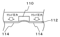
さらに、高度に薄層化されたキャリアにおいては、金型内の樹脂供給路110を挟んだクランプ位置114においてキャリア112にかかるクランプ圧力により、図10に示したように樹脂供給路110の中でキャリアが変形して盛り上がってしまうことがあった。さらに、キャリア112が樹脂供給路110の中で変形したままで樹脂を注入すると、樹脂は紙面垂直な方向から導入されるため、樹脂封止しようとする面の裏側の空間115にも樹脂が回りこんでしまい、図11に示したように、キャリア112の裏側のクランプ位置114の間に樹脂漏れ部分116が生じることが問題となっている。
Further, in the case of a highly thinned carrier, the clamping pressure applied to the
そこで、本発明は上述した実情に鑑みてなされたものであり、樹脂封止のためのトランスファ成型時の不具合を確実に抑制することを可能とする半導体装置樹脂封止用金型を提供することを目的としている。 Accordingly, the present invention has been made in view of the above-described circumstances, and provides a mold for semiconductor device resin sealing that can surely suppress problems during transfer molding for resin sealing. It is an object.
本発明に係る半導体装置樹脂封止用金型は、上述した課題を解決するために、キャリアに半導体素子が搭載される半導体装置をトランスファ成型法により樹脂封止するに際して用いられ、一対の型と、当該型の内部に、前記半導体素子が載置され、トランスファ成型が行われる空間を提供するキャビティおよび当該キャビティに樹脂を供給するためのランナとを備える金型であって、前記キャビティに沿って前記型が対向する部分であって前記キャリアを直接クランプするクランプ領域と、前記クランプ領域で前記キャリアをクランプしたときに、前記キャビティの端部に沿って、前記両方の型のクランプ領域にそれぞれ形成される凸部およびこれに対応する凹部からなる変形付与部と、を含むことを特徴としている。 In order to solve the above-described problems, a mold for semiconductor device resin sealing according to the present invention is used when resin-sealing a semiconductor device in which a semiconductor element is mounted on a carrier by a transfer molding method. A mold including a cavity in which the semiconductor element is mounted and a space for performing transfer molding is provided in the mold, and a runner for supplying resin to the cavity. A clamping region that directly clamps the carrier, which is a portion where the molds face each other, and when the carrier is clamped in the clamping region, is formed in the clamping region of both the molds along the end of the cavity. And a deformation imparting portion composed of a corresponding concave portion.
前記半導体装置樹脂封止用金型において、前記変形付与部が、前記キャビティへの樹脂の導入方向に対して略垂直に形成されていることが好ましい。 In the semiconductor device resin sealing mold, it is preferable that the deformation imparting portion is formed substantially perpendicular to a direction in which the resin is introduced into the cavity.
また、前記半導体装置樹脂封止用金型において、前記変形付与部が、前記キャビティの端部に沿って各型に線状に形成される凹部および凸部で構成されることが好ましい。 Moreover, in the semiconductor device resin sealing mold, it is preferable that the deformation imparting portion is constituted by a concave portion and a convex portion that are linearly formed in each die along the end portion of the cavity.
本発明によれば、キャリアに搭載された半導体素子は型の成型面に設けられたキャビティに載置され、当該キャリアがクランプ領域にてクランプされた後、ランナより供給される樹脂によりトランスファ成型されて封止される。 According to the present invention, the semiconductor element mounted on the carrier is placed in the cavity provided on the molding surface of the mold, and after the carrier is clamped in the clamp region, transfer molding is performed with the resin supplied from the runner. And sealed.
このとき、クランプ領域に設けられた変形付与部により、クランプ領域においてキャリアに凹凸が付与される。これに追従して、ランナ部分においてもキャリアは変形して、樹脂のキャビティへの導入方向に沿って折れ目、くぼみなどが生じることのないようにすることができる。これにより、樹脂封止のためのトランスファ成型時の不具合を確実に抑制することが可能になる。 At this time, unevenness is imparted to the carrier in the clamp region by the deformation imparting portion provided in the clamp region. Following this, the carrier can be deformed also in the runner portion, so that folds, dents and the like do not occur along the direction of introduction of the resin into the cavity. Thereby, it becomes possible to suppress reliably the malfunction at the time of the transfer molding for resin sealing.
本発明によれば、樹脂封止のためのトランスファ成型時の不具合を確実に抑制することが可能になる。 ADVANTAGE OF THE INVENTION According to this invention, it becomes possible to suppress reliably the malfunction at the time of the transfer molding for resin sealing.
以下、本発明に係る半導体装置樹脂封止用金型の実施形態について、図面を参照しながら詳細に説明する。
なお、図面の説明においては、同一要素には同一符号を付し、重複する説明を省略する。
Hereinafter, embodiments of a resin mold for sealing a semiconductor device according to the present invention will be described in detail with reference to the drawings.
In the description of the drawings, the same reference numerals are assigned to the same elements, and duplicate descriptions are omitted.
図1は、前記半導体装置樹脂封止用金型を用いて得られる成型品の一例の概略図である。
図1によれば、半導体素子を備える回路が形成された基板であるキャリア23上に形成した回路を封止するように封止樹脂33が成型され、成型時に樹脂を充填させるための後述するランナの成型部分37およびカルの成型部分35が、キャリア23の端側に連続して形成されている。
FIG. 1 is a schematic view of an example of a molded product obtained by using the semiconductor device resin sealing mold.
According to FIG. 1, a
また、図1には、カルの一方の端面にランナを設けた金型を用いて成型を行って得られる成型品が示されているが、他方の端面にもランナを設けて、この他端側でもキャリアの樹脂封止を行う、すなわちカルの両端でキャリアの樹脂封止を同時に行うようにすることもできる。 Further, FIG. 1 shows a molded product obtained by molding using a mold having a runner on one end face of the cull. It is also possible to carry out resin sealing of the carrier on the side, that is, to carry out resin sealing of the carrier simultaneously at both ends of the cull.
ここで、キャリアは、0.1mm程度の薄基板やテープ状の基板などであり、例えばエポキシ樹脂、BT(ビスマレイミド・トリアジン)レジンなどの樹脂材料から形成することができる。 Here, the carrier is a thin substrate of about 0.1 mm, a tape-shaped substrate, or the like, and can be formed of a resin material such as an epoxy resin or BT (bismaleimide / triazine) resin.
図2は、この成型品の要部の拡大図である。
図2によれば、キャリア23の上であって、ランナの成型部分37が形成されている側の端部39には、後述するクランプ時に前記半導体装置樹脂封止用金型により変形付与された変形部分30が端面に沿って線状に生じている。
FIG. 2 is an enlarged view of a main part of the molded product.
According to FIG. 2, the
本発明の実施形態に係る半導体装置樹脂封止用金型は、このような成型品を得るためのものであって、以下に詳細に説明する。 The mold for resin encapsulation of a semiconductor device according to an embodiment of the present invention is for obtaining such a molded product, and will be described in detail below.
図3は、樹脂封止時に上金型と下金型とで前記キャリア23をクランプした所定の位置の一例、すなわち図2のB−B’に相当する部分を示し、図4はこの状態の要部を拡大した図である。
FIG. 3 shows an example of a predetermined position where the
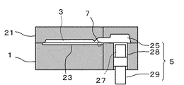
図3では、図2に示したように樹脂供給路を含まないB−B’での断面図が示されており、上金型21と下金型1とでキャリア23をクランプした状態が示される。前記ランナを含まない部分での断面であるため、上金型1の成型面には、半導体素子が載置され、トランスファ成型が行われる空間を提供し、図1の前記封止樹脂33を成型するためのキャビティ3が現れているのみである。
FIG. 3 shows a cross-sectional view at BB ′ not including the resin supply path as shown in FIG. 2, and shows a state in which the
また、図4によれば、下金型1には前記変形部分30を付与するための凸部11が設けられているとともに、上金型23には凸部11に対向するように凹部31が設けられているため、キャリア23は上金型21および下金型1にクランプされると、この凸部11に沿って確実に変形するようになっている。
Further, according to FIG. 4, the
図5は樹脂封止時に上金型と下金型とで前記キャリア23をクランプした別の位置の一例、すなわち図2のA−A’に相当する部分を示し、図6はランナ7にかかる位置でも凸部11を設けたこの状態の要部を拡大した図である。
FIG. 5 shows an example of another position where the
図5では、図2に示したように樹脂供給路を含むA−A’での断面図が示されており、図3と同様に、上金型21と下金型1とでキャリア23をクランプした状態が示される。上金型1の成型面には、前記キャビティ3、当該キャビティ3に樹脂を供給するためのランナ7およびカル25が現れている。
FIG. 5 shows a cross-sectional view taken along the line AA ′ including the resin supply path as shown in FIG. 2. As in FIG. 3, the
また、下金型1には、ポット28が現れており、このポット28内には樹脂27をプランジャ29が設けられるとともに、ポット28内であってプランジャ29の押し出し面には封止用樹脂27が装入されている。また、カル25、ポット28およびプランジャ29により樹脂供給部5が構成される。
Further, a
ここで、プランジャ29は、ポット28から樹脂27を射出する機能を有し、鋼などから構成することができる。また、ポット28に装入される封止用樹脂27としては、熱軟化性樹脂、例えばBステージ化するエポキシ樹脂などを用いることができる。
Here, the
また、図6によれば、下金型1のこの部分にも凸部11が設けられているため、キャリア23は上金型21および下金型1にクランプされると、図4に示したような変形に追従して、この凸部11に沿った変形がより確実になる。
Further, according to FIG. 6, since the
なお、ランナ7が設けられている部分において、凸部が設けられている例を示したが、この部分に凸部が設けられていなくても、ランナ7が設けられている部分以外の前記クランプ領域9で凸部が設けられていれば、クランプ領域9で付与される変形に追従してキャリア23のランナ7内部にかかる部分も同様の変形が生じるようになる。このため、凸部11は、下金型1のランナ7にかかる位置では設けても設けなくても差し支えない。
In addition, although the example in which the convex portion is provided in the portion where the
ここで、変形付与部について説明する。
キャリア23のクランプ時に、ランナ7内でキャリア23が変形してキャリア23の裏側に樹脂が回りこむことがないように、キャリア23のクランプされた部分を凹凸に変形させて、この変形に追従してランナ7の中では樹脂の導入方向Xに沿った変形を妨げるようにキャリア23を変形させることが重要である。
Here, a deformation | transformation provision part is demonstrated.
When the
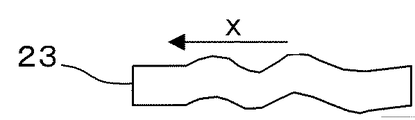
例えば、図4に示したような少なくとも下金型1にキャビティ3の端部に沿って線状に設けた凸部11が挙げられる。このほかに、変形付与部を、図7に示したようにキャリア23が波型に変形するように設けてもよいし、図8に示したように図6の凹凸を逆にした形状にキャリア23が変形するように設けてもよいし、図9に示したようにキャリア23が単に折れ込む形状に変形するように設けてもよい。また、凹凸は、一対であっても、それ以上の対であってもよい。
For example, the
本実施形態によれば、半導体素子を実装したキャリアが所定の温度、例えば175℃に加熱された本実施形態の金型に搬送され、当該金型内に設けられたキャビティに載置されると、上金型21および下金型1によりクランプされる。続いて、プランジャ29が上昇し、樹脂27がカル25に押し出され、ランナ7を通ってキャビティ3に到達して、前記半導体素子は封止される。
According to the present embodiment, when the carrier on which the semiconductor element is mounted is transported to the mold of the present embodiment heated to a predetermined temperature, for example, 175 ° C., and placed on the cavity provided in the mold. The
このとき、クランプ領域9に設けられた凸部11により、クランプ領域9においてキャリア3に凹凸が付与され、樹脂の導入方向Xに沿って折れ目、くぼみなどが生じることのないようにすることができる。これにより、樹脂封止のためのトランスファ成型時の不具合、例えばキャリア23の裏側に樹脂が回ったり、樹脂が金型から漏れたりといった不具合を確実に抑制することが可能になる。
At this time, the
以上、半導体装置樹脂封止用金型の実施形態について説明したが、これに限定されることはなく、本発明の目的を逸脱しない範囲で適宜変更可能なことは言うまでもない。
例えば、下金型の成型面であって上金型側に、キャビティ、ランナ、カルなどを設けた例を説明したが、これら全部または一部を下金型側に設けてもよい。同様に、樹脂供給部を下金型に設けた例を示したが、上金型に設けても差し支えない。
As mentioned above, although embodiment of the metal mold | die for semiconductor device resin was demonstrated, it is not limited to this, It cannot be overemphasized that it can change suitably in the range which does not deviate from the objective of this invention.
For example, an example has been described in which a cavity, a runner, a cull, and the like are provided on the molding surface of the lower mold on the upper mold side, but all or a part of these may be provided on the lower mold side. Similarly, although the example in which the resin supply unit is provided in the lower mold is shown, it may be provided in the upper mold.
1 下金型
3 キャビティ
5 樹脂供給部
7 ランナ
9 クランプ領域
11 凸部
21 上金型
23 キャリア
DESCRIPTION OF
Claims (3)
前記キャビティに沿って前記型が対向する部分であって前記キャリアを直接クランプするクランプ領域と、
前記クランプ領域で前記キャリアをクランプしたときに、前記キャビティの端部に沿って、前記両方の型のクランプ領域にそれぞれ形成される凸部およびこれに対応する凹部からなる変形付与部と、
を含むことを特徴とする半導体装置樹脂封止用金型。 Used when resin-sealing a semiconductor device on which a semiconductor element is mounted on a carrier by a transfer molding method. A pair of molds and a space in which the semiconductor elements are placed and transferred are provided inside the mold. A mold including a cavity to be run and a runner for supplying resin to the cavity,
A clamping region that directly clamps the carrier at a portion where the mold faces along the cavity;
When the carrier is clamped in the clamp region, along the end of the cavity, a deformation imparting portion comprising a convex portion and a concave portion corresponding to the convex portion respectively formed in the clamp regions of both types,
A mold for resin encapsulation of a semiconductor device, comprising:
前記変形付与部が、前記キャビティへの樹脂の導入方向に対して略垂直に形成されていることを特徴とする半導体装置樹脂封止用金型。 In the metal mold for resin sealing of a semiconductor device according to claim 1,
The semiconductor device resin-sealing mold, wherein the deformation imparting portion is formed substantially perpendicular to the direction of introduction of the resin into the cavity.
前記変形付与部が、前記キャビティの端部に沿って各型に線状に形成される凹部および凸部で構成されることを特徴とする半導体装置樹脂封止用金型。 In the metal mold for resin sealing of a semiconductor device according to claim 1,
The semiconductor device resin-sealing mold, wherein the deformation imparting portion includes a concave portion and a convex portion that are linearly formed on each die along the end portion of the cavity.
Priority Applications (1)
| Application Number | Priority Date | Filing Date | Title |
|---|---|---|---|
| JP2004102445A JP2005294293A (en) | 2004-03-31 | 2004-03-31 | Metal mold for sealing semiconductor device with resin |
Applications Claiming Priority (1)
| Application Number | Priority Date | Filing Date | Title |
|---|---|---|---|
| JP2004102445A JP2005294293A (en) | 2004-03-31 | 2004-03-31 | Metal mold for sealing semiconductor device with resin |
Publications (1)
| Publication Number | Publication Date |
|---|---|
| JP2005294293A true JP2005294293A (en) | 2005-10-20 |
Family
ID=35326933
Family Applications (1)
| Application Number | Title | Priority Date | Filing Date |
|---|---|---|---|
| JP2004102445A Pending JP2005294293A (en) | 2004-03-31 | 2004-03-31 | Metal mold for sealing semiconductor device with resin |
Country Status (1)
| Country | Link |
|---|---|
| JP (1) | JP2005294293A (en) |
-
2004
- 2004-03-31 JP JP2004102445A patent/JP2005294293A/en active Pending
Similar Documents
| Publication | Publication Date | Title |
|---|---|---|
| KR100198685B1 (en) | Semiconductor device manufacturing method and mold assembly thereof | |
| KR950000512B1 (en) | Mold for transfer molding | |
| US20020017738A1 (en) | Resin sealing method and resin sealing apparatus | |
| JP5892683B2 (en) | Resin sealing method | |
| US8163220B2 (en) | Method of packaging integrated circuits | |
| JP2005294293A (en) | Metal mold for sealing semiconductor device with resin | |
| JP2002343819A (en) | Resin sealing method and substrate clamping mechanism | |
| CN100536100C (en) | Resin sealing shaping device for electronic parts | |
| JP4563426B2 (en) | Resin mold | |
| JP5234884B2 (en) | Resin sealing mold | |
| WO2014029176A1 (en) | Clamp for reducing bending in package and method therefor | |
| KR100646905B1 (en) | Resin seal mold | |
| JP5903785B2 (en) | Semiconductor device manufacturing method | |
| KR0162887B1 (en) | Molding method and mold mold apparatus of semiconductor package | |
| US5134458A (en) | Long size lead frame for semiconductor elements | |
| KR20170048466A (en) | Lead frame and method for manufacturing semiconductor dece | |
| JP2016076640A (en) | Semiconductor cooling structure | |
| JP2761193B2 (en) | Lead frame to which external leads are fixed, semiconductor device using the same, and method of manufacturing the same | |
| JP4606126B2 (en) | Molding apparatus and resin molding method | |
| JPH04341812A (en) | Injection molding method | |
| JP5625673B2 (en) | Injection molding method and apparatus | |
| JP2570157B2 (en) | Mold for resin sealing | |
| JPS63181438A (en) | Metal mold for plastic sealing of semiconductor device | |
| JP2005158873A (en) | Manufacturing method of semiconductor device | |
| JPH04152109A (en) | Resin mold |
Legal Events
| Date | Code | Title | Description |
|---|---|---|---|
| A621 | Written request for application examination |
Effective date: 20070112 Free format text: JAPANESE INTERMEDIATE CODE: A621 |
|
| A977 | Report on retrieval |
Free format text: JAPANESE INTERMEDIATE CODE: A971007 Effective date: 20080818 |
|
| A131 | Notification of reasons for refusal |
Effective date: 20090811 Free format text: JAPANESE INTERMEDIATE CODE: A131 |
|
| A521 | Written amendment |
Effective date: 20091013 Free format text: JAPANESE INTERMEDIATE CODE: A523 |
|
| A02 | Decision of refusal |
Effective date: 20091104 Free format text: JAPANESE INTERMEDIATE CODE: A02 |