JP2005294061A - LED lighting device and lighting apparatus - Google Patents
LED lighting device and lighting apparatus Download PDFInfo
- Publication number
- JP2005294061A JP2005294061A JP2004107977A JP2004107977A JP2005294061A JP 2005294061 A JP2005294061 A JP 2005294061A JP 2004107977 A JP2004107977 A JP 2004107977A JP 2004107977 A JP2004107977 A JP 2004107977A JP 2005294061 A JP2005294061 A JP 2005294061A
- Authority
- JP
- Japan
- Prior art keywords
- light emitting
- emitting diode
- current
- resistor
- inductor
- Prior art date
- Legal status (The legal status is an assumption and is not a legal conclusion. Google has not performed a legal analysis and makes no representation as to the accuracy of the status listed.)
- Granted
Links
Images


Landscapes
- Led Devices (AREA)
- Non-Portable Lighting Devices Or Systems Thereof (AREA)
- Circuit Arrangement For Electric Light Sources In General (AREA)
Abstract
【課題】発光ダイオードを高効率で点灯させるとともに電流設定用の抵抗を過電流から保護することのできるLED点灯装置および照明器具を提供する。
【解決手段】LED点灯装置1は、インダクタL1と共に直流電源2に直列的に接続される発光ダイオード3および抵抗R1と、直流電源2と、インダクタL1、発光ダイオード3および抵抗R1との接続を開閉するスイッチング手段FET1と、スイッチング手段FET1がオフのときに、インダクタL1、発光ダイオード3および抵抗R1とともに閉回路を形成するように接続されたダイオードD1と、直流電源2、スイッチング素子FET1、インダクタL1、発光ダイオード3および抵抗R1の直列回路に介挿され、この直列回路に所定値以上の電流が流れたときに直列回路を遮断する回路遮断手段6を具備している。
【選択図】図1An LED lighting device and a lighting fixture capable of lighting a light emitting diode with high efficiency and protecting a current setting resistor from an overcurrent.
An LED lighting device 1 opens and closes a connection between a light emitting diode 3 and a resistor R1 connected in series to a DC power supply 2 together with an inductor L1, and a connection between the DC power supply 2, the inductor L1, the light emitting diode 3 and the resistor R1. Switching means FET1, a diode D1 connected to form a closed circuit with the inductor L1, the light emitting diode 3 and the resistor R1 when the switching means FET1 is off, a DC power supply 2, a switching element FET1, an inductor L1, A circuit interrupting means 6 is provided which is inserted in a series circuit of the light emitting diode 3 and the resistor R1 and interrupts the series circuit when a current of a predetermined value or more flows through the series circuit.
[Selection] Figure 1
Description
本発明は、発光ダイオードを点灯させるLED点灯装置および照明器具に関する。 The present invention relates to an LED lighting device and a lighting fixture for lighting a light emitting diode.
直流電源によりインダクタが励磁され、直流電源のオフ時にインダクタに蓄積された電磁エネルギーによる回生電流を発光ダイオードに流して、発光ダイオードを高効率で点灯させるLED点灯装置が知られている。すなわち、直流電源にスイッチング素子を介してインダクタおよび発光ダイオードの直列回路が接続され、この直列回路に並列的に接続され、スイッチング素子のオフ時に当該直列回路と閉回路を形成するダイオードを有するLED点灯装置が知られている(例えば、特許文献1参照。)。このLED点灯装置は、発光ダイオードに所定の電流が流れるようにするために、発光ダイオードに直列的に抵抗が接続される。
特許文献1において、発光ダイオードに直接的に接続される抵抗の抵抗値が大きいと、通常点灯時、抵抗で消費される電力が大きくなるという問題がある。また、抵抗の抵抗値を小さくすると、例えばスイッチング素子が短絡して過電流が流れたときに、抵抗が焼損するという問題がある。
In
本発明は、発光ダイオードを高効率で点灯させるとともに電流設定用の抵抗を過電流から保護することのできるLED点灯装置および照明器具を提供することを目的とする。 An object of the present invention is to provide an LED lighting device and a lighting fixture capable of lighting a light emitting diode with high efficiency and protecting a current setting resistor from an overcurrent.
請求項1に記載のLED点灯装置の発明は、直流電源と;直流電源によって励磁されるインダクタと;インダクタと共に直流電源に直列的に接続された発光ダイオードと;発光ダイオードに直列的に接続された抵抗と;直流電源と、インダクタ、発光ダイオードおよび抵抗との接続を開閉するスイッチング手段と;スイッチング手段がオフのときに、インダクタ、発光ダイオードおよび抵抗とともに閉回路を形成するように接続されたダイオードと;発光ダイオードに流れる電流を検出する電流検出手段と;電流検出手段により検出された電流に応じてスイッチング手段のオンオフ動作を制御する制御手段と;直流電源、スイッチング手段、インダクタ、発光ダイオードおよび抵抗の直列回路に介挿され、この直列回路に所定値以上の電流が流れたときに直列回路を遮断する回路遮断手段と;を具備していることを特徴とする。
The invention of the LED lighting device according to
本発明および以下の各発明において、特に言及しない限り、各構成は以下による。 In the present invention and each of the following inventions, each configuration is as follows unless otherwise specified.
直流電源は、バッテリ、交流電圧を整流または整流平滑したものなど、直流電圧を出力するものであればよい。 The DC power supply may be anything that outputs a DC voltage, such as a battery or a rectified or rectified smoothed AC voltage.
発光ダイオードは、面実装形または砲弾形のいずれであってもよい。また、1個または複数個のどちらであってもよく、複数個の場合、直列接続または直並列接続を許容する。 The light emitting diode may be either surface-mounted or bullet-shaped. Further, either one or a plurality of them may be used, and in the case of a plurality, a series connection or a series-parallel connection is allowed.
抵抗は、発光ダイオードに流れる電流を設定する。 The resistor sets a current flowing through the light emitting diode.
電流検出手段は、直接的に検出してもよく、発光ダイオードに流れる電流に相当する電流を検出するものもよい。 The current detection means may detect directly or may detect current corresponding to the current flowing through the light emitting diode.
「所定値以上の電流」とは、抵抗に連続的に電流が流れても、抵抗が熱損傷や熱破壊しない電流値をいい、抵抗の定格容量などに応じて適宜設定される。 “Current greater than or equal to a predetermined value” refers to a current value at which the resistor is not thermally damaged or destroyed even when a current continuously flows through the resistor, and is appropriately set according to the rated capacity of the resistor.
本発明によれば、例えば、外部からの過電圧によりスイッチング手段が短絡破壊され、直流電源、スイッチング手段、インダクタ、発光ダイオードおよび抵抗の直列回路に所定値以上の電流が流れたときに、回路遮断手段により直列回路が遮断されて直列回路に電流が流れなくなる。 According to the present invention, for example, when the switching means is short-circuit broken due to an overvoltage from the outside, and a current exceeding a predetermined value flows through a series circuit of the DC power supply, the switching means, the inductor, the light emitting diode, and the resistor, the circuit interruption means As a result, the series circuit is interrupted and no current flows through the series circuit.
請求項2に記載のLED点灯装置の発明は、請求項1記載のLED点灯装置において、回路遮断手段は、非自己復帰形部品であることを特徴とする。
The invention of the LED lighting device according to
非自己復帰形部品は、例えばヒューズなどである。 The non-self-returning part is, for example, a fuse.
本発明によれば、回路遮断手段は、非自己復帰形部品であるので、直流電源、スイッチング手段、インダクタ、発光ダイオードおよび抵抗の直列回路に所定値以上の電流が流れたときに、継続して直列回路が遮断される。 According to the present invention, since the circuit interruption means is a non-self-reset type component, when a current exceeding a predetermined value flows through the series circuit of the DC power supply, the switching means, the inductor, the light emitting diode, and the resistor, The series circuit is interrupted.
請求項3に記載のLED点灯装置の発明は、直流電源と;直流電源によって励磁されるインダクタと;インダクタと共に直流電源に直列的に接続された発光ダイオードと;発光ダイオードに直列的に接続された抵抗と;直流電源と、インダクタ、発光ダイオードおよび抵抗との接続を開閉するスイッチング手段と;スイッチング手段がオフのときに、インダクタ、発光ダイオードおよび抵抗とともに閉回路を形成するように接続されたダイオードと;発光ダイオードに流れる電流を検出する電流検出手段と;電流検出手段により検出された電流に応じてスイッチング手段のオンオフ動作を制御する制御手段と;直流電源、スイッチング手段、インダクタ、発光ダイオードおよび抵抗の直列回路に介挿され、この直列回路に所定値以上の電流が流れないように電流を制限する電流制限手段と;を具備していることを特徴とする。
The invention of the LED lighting device according to
電流制限手段は、所定値以上の電流が流れるときに、直流電源、スイッチング手段、インダクタ、発光ダイオードおよび抵抗の直列回路に直列接続される限流要素例えば抵抗である。 The current limiting means is a current limiting element such as a resistor connected in series to a series circuit of a DC power source, a switching means, an inductor, a light emitting diode, and a resistor when a current of a predetermined value or more flows.
本発明によれば、例えば、外部からの過電圧によりスイッチング手段が短絡破壊され、直流電源、スイッチング手段、インダクタ、発光ダイオードおよび抵抗の直列回路に所定値以上の電流が流れたときに、電流制限手段により直列回路に所定値以上の電流が流れないように制限される。 According to the present invention, for example, when the switching means is short-circuited and broken by an overvoltage from the outside, and a current exceeding a predetermined value flows through a series circuit of the DC power supply, the switching means, the inductor, the light emitting diode, and the resistor, the current limiting means Thus, a current exceeding a predetermined value does not flow through the series circuit.
請求項4に記載のLED点灯装置の発明は、請求項3記載のLED点灯装置において、電流制限手段は、電流が大きくなるにつれインピーダンスが大きくなる電気素子であることを特徴とする。 According to a fourth aspect of the present invention, there is provided the LED lighting device according to the third aspect, wherein the current limiting means is an electric element whose impedance increases as the current increases.
電気素子は、例えば正特性サーミスタである。そして、電流が大きくなるにつれ、温度上昇してインピーダンスが大きくなる。 The electric element is, for example, a positive characteristic thermistor. As the current increases, the temperature rises and the impedance increases.
本発明によれば、直流電源、スイッチング手段、インダクタ、発光ダイオードおよび抵抗の直列回路に所定値以上の電流が流れたときに、直列回路に直列的に接続される電気素子のインピーダンス大きくなり、直列回路に所定値以上の電流が流れなくなる。 According to the present invention, when a current exceeding a predetermined value flows through a series circuit of a DC power supply, switching means, inductor, light emitting diode, and resistor, the impedance of the electrical elements connected in series to the series circuit increases. The current exceeding the predetermined value does not flow in the circuit.
請求項5に記載の照明器具の発明は、請求項1ないし4いずれか一記載のLED点灯装置と;このLED点灯装置を配設している照明器具本体と;を具備していることを特徴とする。
The invention of a lighting fixture according to
本発明によれば、請求項1ないし4いずれか一記載のLED点灯装置を具備しているので、直流電源、スイッチング手段、インダクタ、発光ダイオードおよび抵抗の直列回路に所定値以上の電流が流れたときに、発光ダイオードに流れる電流を設定する抵抗の熱破壊が防止される照明器具が提供される。
According to the present invention, since the LED lighting device according to any one of
請求項1の発明によれば、直流電源、スイッチング手段、インダクタ、発光ダイオードおよび抵抗の直列回路に所定値以上の電流が流れたときに、回路遮断手段により直列回路が遮断されるので、発光ダイオードに流れる電流を設定する抵抗値の小さい抵抗の熱破壊を防止することができ、回路基板から落下することを防止することができる。 According to the first aspect of the present invention, when the current exceeding a predetermined value flows through the series circuit of the DC power source, the switching means, the inductor, the light emitting diode, and the resistor, the series circuit is interrupted by the circuit interrupting means. It is possible to prevent thermal destruction of a resistor having a small resistance value that sets the current flowing through the circuit board, and to prevent the resistor from falling from the circuit board.
請求項2の発明によれば、直流電源、スイッチング手段、インダクタ、発光ダイオードおよび抵抗の直列回路に所定値以上の電流が流れたときに、非自己復帰形部品により継続して直列回路が遮断されるので、ダイオードに流れる電流を設定する抵抗の熱破壊をより安全に防止することができる。
According to the invention of
請求項3の発明によれば、直流電源、スイッチング手段、インダクタおよび発光ダイオードの直列回路に所定値以上の電流が流れたときに、電流制限手段により直列回路に所定値以上の電流が流れないように制限されるので、ダイオードに流れる電流を設定する抵抗の熱破壊を防止することができ、回路基板から落下することを防止することができる。
According to the invention of
請求項4の発明によれば、直流電源、スイッチング手段、インダクタ、発光ダイオードおよび抵抗の直列回路に所定値以上の電流が流れたときに、直列回路に直列的に接続される電気素子のインピーダンス大きくなって、直列回路に所定値以上の電流が流れなくなるので、ダイオードに流れる電流を設定する抵抗の熱破壊を防止することができる。
According to the invention of
請求項5の発明によれば、請求項1ないし4いずれか一記載のLED点灯装置を具備しているので、ダイオードに流れる電流を設定する抵抗が熱破壊して回路基板から落下することが防止され、照明器具本体が熱損傷されにくい照明器具を提供することができる。
According to the invention of
以下、本発明の一実施の形態について、図面を参照して説明する。まず、本発明の第1の実施形態について説明する。 Hereinafter, an embodiment of the present invention will be described with reference to the drawings. First, a first embodiment of the present invention will be described.
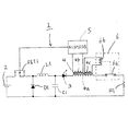
図1は、本発明の第1の実施形態を示すLED点灯装置の回路図である。LED点灯装置1は、直流電源2、インダクタL1、発光ダイオード3、スイッチング手段としての電界効果トランジスタFET1、ダイオードD1、抵抗R1、電流検出手段としての電流検出回路4、制御手段としての制御回路5および回路遮断手段としてのリレー6を有して構成されている。
FIG. 1 is a circuit diagram of an LED lighting device showing a first embodiment of the present invention. The
直流電源2は、例えば商用交流電圧を整流平滑して直流電圧を出力するように形成されている。インダクタL1は、直流電源2から供給される電流によって励磁され、電磁エネルギーが蓄積される。発光ダイオード3は、抵抗R1を直列的に接続し、さらにインダクタL1と共に直流電源2に直列的に接続されている。そして、発光ダイオード3は、電流が流れると、例えば白色光を放射するように形成されている。また、抵抗R1は、発光ダイオード3に流れる電流を設定するものであり、低抵抗値に設定している。
The
電界効果トランジスタFET1は、制御回路5によりオンオフ制御され、直流電源2と、インダクタL1、発光ダイオード3および抵抗R1との接続を開閉する。そして、ダイオードD1は、インダクタL1、発光ダイオード3、抵抗R1、電流検出回路4およびリレー接点6aの直列回路と並列的に接続され、電界効果トランジスタFET1がオフのときに、当該直列回路とともに閉回路を形成している。
The field effect transistor FET1 is ON / OFF controlled by the
電流検出回路4は、1次巻線4aが発光ダイオード3と直列的に接続され、発光ダイオード3に流れる電流を2次巻線4bで検出して制御回路5に出力するように構成されている。
In the
制御回路5は、電流検出回路4により検出された電流に応じて電界効果トランジスタFET1のオンオフ動作を制御するように構成されている。すなわち、発光ダイオード3に流れる電流が予め設定された一定の電流値となるように、電界効果トランジスタFET1のオン期間およびオフ期間を調整する。
The
リレー接点6aは、リレー6の常閉接点であり、電流検出回路4を介して発光ダイオード3と直列的に接続されている。そして、リレーコイル6bは、電流検出回路4の3次巻線4cに接続されている。リレーコイル6bは、発光ダイオード3に流れる電流が予め設定された所定値以上の電流であると、リレー接点6aを開路させる。これにより、直流電源2と発光ダイオード3との接続が遮断され、発光ダイオード3に電流が流れなくなる。
The relay contact 6 a is a normally closed contact of the relay 6, and is connected in series with the
リレー接点6aは、直流電源2、電界効果トランジスタFET1、インダクタL1、発光ダイオード3および抵抗R1の直列回路のいずれかの箇所に介挿されていればよい。すなわち、当該直列回路に流れる電流は、抵抗R1に流れる電流であるので、当該直列回路に所定値以上の電流が流れたときに、リレー接点6aを開路させ、当該直列回路を遮断するようにしてもよい。
The relay contact 6a only needs to be inserted in any part of the series circuit of the
なお、インダクタL1および発光ダイオード3間に、発光ダイオード3と並列的に平滑用コンデンサC1が接続されている。平滑用コンデンサC1により、例えば発光ダイオード3の接続が確認される。すなわち、直流電源2が投入されたにも係わらず発光ダイオード3が点灯しないとき、平滑用コンデンサC1の両端間に所定の電圧が検出されると、発光ダイオード3に接続されているリード線が断線しているなど、発光ダイオード3が接続されていないことを確認できる。
A smoothing capacitor C1 is connected in parallel with the
次に、LED点灯装置1の動作について述べる。
Next, the operation of the
直流電源2が投入されると、制御回路5は、電界効果トランジスタFET1をオンオフ制御する。そして、電界効果トランジスタFET1がオンすると、直流電源2から供給される電流が、電界効果トランジスタFET1、インダクタL1、発光ダイオード3、電流検出回路4、リレー接点6aおよび抵抗R1の経路で流れ、発光ダイオード3が点灯するとともに、インダクタL1に電磁エネルギーが蓄積される。そして、電界効果トランジスタFET1がオフすると、インダクタL1に蓄積された電磁エネルギーによる電流が、インダクタL1、発光ダイオード3、電流検出回路4、リレー接点6a、抵抗R1およびダイオードD1の閉回路内で流れ、発光ダイオード3が点灯するとともに、インダクタL1の電磁エネルギーが消費される。このインダクタL1に蓄積された電磁エネルギーによる回生電流により発光ダイオード3が点灯され、また、抵抗R1の抵抗値が小さく、抵抗R1での消費電力が小さいので、発光ダイオード3は高効率で点灯される。
When the
制御回路5は、電流検出回路4が検出した発光ダイオード3に流れる電流が予め設定された一定の電流値となるように、電界効果トランジスタFET1のオン期間およびオフ期間を調整する。
The
そして、外部電源から直流電源2に過電圧が重畳され、この過電圧が電界効果トランジスタFET1に印加されるなどして、電界効果トランジスタFET1が破壊されて短絡すると、直流電源2からの電流が電界効果トランジスタFET1、インダクタL1、発光ダイオード3、電流検出回路4、リレー接点6aおよび抵抗R1の経路で連続的に流れる。このとき、インダクタL1の抵抗値、電流検出回路4の1次巻線4aの抵抗値、および抵抗R1の抵抗値はそれぞれ小さいので、過電流が流れるようになる。
Then, when an overvoltage is superimposed on the
過電流が予め設定された所定値以上の電流であると、リレーコイル6bが付勢され、直流電源2、電界効果トランジスタFET1、インダクタL1、発光ダイオード3、電流検出回路4、リレー接点6aおよび抵抗R1の直列回路より、リレー接点6aが開路し、当該直列回路が遮断されて電流が流れなくなる。
If the overcurrent is equal to or greater than a predetermined value set in advance, the relay coil 6b is energized, and the
前記所定値は、直流電源2、電界効果トランジスタFET1、インダクタL1、発光ダイオード3、電流検出回路4、リレー接点6aおよび抵抗R1の直列回路に連続的に電流が流れても、抵抗値の小さい抵抗R1が熱破壊されない電流値に設定されている。したがって、当該直列回路に所定値以上の電流が流れたときに、当該直列回路を遮断することにより、抵抗R1の熱破壊が防止され、回路基板からの落下が防止される。
The predetermined value is a resistance having a small resistance value even when a current continuously flows through a series circuit of the
次に、本発明の第2の実施形態について説明する。 Next, a second embodiment of the present invention will be described.
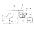
図2〜図3は、本発明の第2の実施形態を示すLED点灯装置の回路図である。なお、図1と同一部分には部分には同一符号を付して説明は省略する。 2 to 3 are circuit diagrams of an LED lighting device showing a second embodiment of the present invention. In addition, the same code | symbol is attached | subjected to a part same as FIG. 1, and description is abbreviate | omitted.
図2に示すLED点灯装置7は、図1に示すLED点灯装置1において、リレー接点6aに代えて、回路遮断手段としてのパターンヒューズ8を接続したものである。このヒューズ8は、非自己復帰形部品であり、所定値以上の電流が流れたときに溶融するものに選定されている。
An
例えば、電界効果トランジスタFET1が破壊短絡して、直流電源2、電界効果トランジスタFET1、インダクタL1、発光ダイオード3、電流検出回路4、ヒューズ8および抵抗R1の直列回路に所定値以上の電流が流れたときに、ヒューズ8が溶融して当該直列回路を遮断するので、抵抗値の小さい抵抗R1の熱破壊が防止される。
For example, the field-effect transistor FET1 is destroyed and short-circuited, and a current of a predetermined value or more flows through the series circuit of the
また、図3に示すLED点灯装置9は、図1に示すLED点灯装置1において、リレー接点6aに代えて、電流検出回路4の1次巻線4aの一端に回路遮断手段としての低融点金属線10を接続し、この低融点金属線10がリード線11を介して発光ダイオード3に接続されているものである。低融点金属線10は、放熱されにくく配線されている。そして、低融点金属線10は、所定値以上の電流が流れたときに溶断する。
Further, the
例えば、電界効果トランジスタFET1が破壊短絡して、直流電源2、電界効果トランジスタFET1、インダクタL1、発光ダイオード3、低融点金属線10、電流検出回路4および抵抗R1の直列回路に所定値以上の電流が流れたときに、低融点金属線10が溶断して当該直列回路を遮断するので、抵抗値の小さい抵抗R1の熱破壊が防止される。
For example, the field effect transistor FET1 is destructively short-circuited, and a current exceeding a predetermined value flows in a series circuit of the
次に、本発明の第3の実施形態について説明する。 Next, a third embodiment of the present invention will be described.
図4は、本発明の第3の実施形態を示すLED点灯装置の回路図である。なお、図2と同一部分には部分には同一符号を付して説明は省略する。 FIG. 4 is a circuit diagram of an LED lighting device showing a third embodiment of the present invention. In addition, the same code | symbol is attached | subjected to a part same as FIG. 2, and description is abbreviate | omitted.
図4に示すLED点灯装置12は、図2に示すLED点灯装置7において、電流検出回路4と抵抗R1を兼用した抵抗R2を発光ダイオード3に直列的に接続したものである。
The
そして、抵抗R2に流れる電流が電圧に変換されて制御回路5に入力される。そして、電流検出回路4と抵抗R1を兼用しているので、LED点灯装置12が簡素化される。
Then, the current flowing through the resistor R2 is converted into a voltage and input to the
次に、本発明の第4の実施形態について説明する。 Next, a fourth embodiment of the present invention will be described.
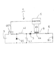
図5は、本発明の第4の実施形態を示すLED点灯装置の回路図である。なお、図1と同一部分には部分には同一符号を付して説明は省略する。 FIG. 5 is a circuit diagram of an LED lighting device showing a fourth embodiment of the present invention. In addition, the same code | symbol is attached | subjected to a part same as FIG. 1, and description is abbreviate | omitted.
図5に示すLED点灯装置13は、図1に示すLED点灯装置1において、リレー接点6aと並列的に抵抗R3が接続されたものである。リレー接点6aおよび抵抗R3は、電流制限手段を形成している。
The LED lighting device 13 shown in FIG. 5 is obtained by connecting a resistor R3 in parallel with the relay contact 6a in the
抵抗R3は、リレー接点6aが開路したときに、直流電源2、電界効果トランジスタFET1、インダクタL1、発光ダイオード3、電流検出回路4および抵抗R1の直列回路に直列的に接続され、当該直列回路に所定値以上の電流が流れないように抵抗値が予め設定されている。
When the relay contact 6a is opened, the resistor R3 is connected in series to the series circuit of the
そして、外部からの過電圧などにより電界効果トランジスタFET1が破壊短絡すると、直流電源2からの電流が電界効果トランジスタFET1、インダクタL1、発光ダイオード3、電流検出回路4、リレー接点6aおよび抵抗R1の経路で過電流となって連続的に流れる。このとき、過電流は、電流検出回路4の3次巻線4cで検出され、過電流が予め設定された所定値以上の電流であるとき、リレーコイル6bが付勢される。これにより、リレー接点6aが開路され、直流電源2に電界効果トランジスタFET1、インダクタL1、発光ダイオード3、電流検出回路4、抵抗R3および抵抗R1の直列回路が接続され、当該直列回路に所定値を下回る電流が流れるようになる。したがって、抵抗値の小さい抵抗R1の熱破壊などが防止される。
When the field effect transistor FET1 is destroyed and short-circuited due to an external overvoltage or the like, the current from the
次に、本発明の第5の実施形態について説明する。 Next, a fifth embodiment of the present invention will be described.
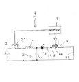
図6は、本発明の第5の実施形態を示すLED点灯装置の回路図である。なお、図2と同一部分には部分には同一符号を付して説明は省略する。 FIG. 6 is a circuit diagram of an LED lighting device showing a fifth embodiment of the present invention. In addition, the same code | symbol is attached | subjected to a part same as FIG. 2, and description is abbreviate | omitted.
図6に示すLED点灯装置14は、図2に示すLED点灯装置7において、回路遮断手段としてのヒューズ8に代えて、電流制限手段としての正特性サーミスタ15が接続されたものである。サーミスタ15は、電流が大きくなるにつれインピーダンスが大きくなる電気素子である。すなわち、サーミスタ15は、発光ダイオード3に予め設定された一定の電流値が流れているときにはその抵抗値が非常に小さく、過電流が流れるとその抵抗値が大きくなり、発光ダイオード3に所定値以上の電流が連続的に流れないようにその電気特性が予め選定されている。また、サーミスタ15は、抵抗R1を兼ねている。
The
例えば、電界効果トランジスタFET1が破壊短絡して、直流電源2、電界効果トランジスタFET1、インダクタL1、発光ダイオード3、電流検出回路4およびサーミスタ15の直列回路に所定値以上の電流が流れたときに、サーミスタ15の抵抗値(インピーダンス)が大きくなり、当該直列回路に所定値以上の電流が流れなくなる。したがって、インダクタL1や発光ダイオード3などの回路部品の熱損傷や破壊などが防止される。
For example, when the field effect transistor FET1 is destroyed and short-circuited and a current of a predetermined value or more flows through a series circuit of the
次に、本発明の第6の実施形態について説明する。 Next, a sixth embodiment of the present invention will be described.
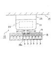
図7は、本発明の第6の実施形態を示すLED照明器具の一部切り欠き概略側面図である。なお、図1と同一部分には同一符号を付して説明は省略する。 FIG. 7 is a partially cutaway schematic side view of an LED lighting apparatus showing a sixth embodiment of the present invention. Note that the same parts as those in FIG.
図7に示す照明器具16は、天井面17に配設される直付け照明器具であり、図1に示すLED点灯装置1および照明器具本体18を有して構成されている。
A
照明器具本体18は、下面に開口18aを有して箱状に形成され、内部に基板19を配設している。基板19には、直列接続された複数の発光ダイオード3が開口18aに臨んで配設されている。そして、照明器具本体18は、上面側に設けられた所定長の連結管20,20によりアダプタ21に支持されている。
The luminaire
アダプタ21は、略円柱状に形成され、内部にLED用点灯装置22を収納している。LED用点灯装置22は、LED点灯装置1より発光ダイオード3が除去されたものである。そして、アダプタ21は、天井面17に配設された引掛シーリング23に接続されている。そして、LED用点灯装置22の出力端子からリード線24,24が導出され、このリード線24,24は、連結管20,20内を挿通して基板19に接続されている。
The
照明器具16は、LED用点灯装置22に所定値以上の電流(過電流)が流れたときに、発光ダイオード3に流れる電流を設定する抵抗値の小さい抵抗R1が保護されるので、当該抵抗R1が熱破壊して基板19から落下することが防止されている。
In the
なお、照明器具本体18は、箱状に限定されるものではなく、円状など、その形状は問わない。また、照明器具16は、直付け形照明器具に限らず、吊り下げ形照明器具、ダウンライトなどの埋込形照明器具など、その用途は問わない。
In addition, the lighting fixture
D1…ダイオード
FET1…スイッチング素子としての電界効果トランジスタ
L1…インダクタ
R1…抵抗
R3…電流制限手段としての抵抗
1,7,9,12,13,14…LED点灯装置
2…直流電源
3…発光ダイオード
4…電流検出手段としての電流検出回路
5…制御手段としての制御回路
6…回路遮断手段としてのリレー
8…回路遮断手段としてのヒューズ
10…回路遮断手段としての低融点金属線
13…電流制限手段としての抵抗
15…電流制限手段としてのサーミスタ
16…照明器具
18…照明器具本体
D1 ... Diode FET1 ... Field effect transistor L1 as a switching element ... Inductor R1 ... Resistance R3 ...
Claims (5)
直流電源によって励磁されるインダクタと;
インダクタと共に直流電源に直列的に接続された発光ダイオードと;
発光ダイオードに直列的に接続された抵抗と;
直流電源と、インダクタ、発光ダイオードおよび抵抗との接続を開閉するスイッチング手段と;
スイッチング手段がオフのときに、インダクタ、発光ダイオードおよび抵抗とともに閉回路を形成するように接続されたダイオードと;
発光ダイオードに流れる電流を検出する電流検出手段と;
電流検出手段により検出された電流に応じてスイッチング手段のオンオフ動作を制御する制御手段と;
直流電源、スイッチング手段、インダクタ、発光ダイオードおよび抵抗の直列回路に介挿され、この直列回路に所定値以上の電流が流れたときに直列回路を遮断する回路遮断手段と;
を具備していることを特徴とするLED点灯装置。 DC power supply;
An inductor excited by a DC power source;
A light emitting diode connected in series with a DC power source together with an inductor;
A resistor connected in series with the light emitting diode;
Switching means for opening and closing a connection between the DC power source and the inductor, the light emitting diode and the resistor;
A diode connected to form a closed circuit with the inductor, the light emitting diode and the resistor when the switching means is off;
Current detection means for detecting current flowing in the light emitting diode;
Control means for controlling the on / off operation of the switching means according to the current detected by the current detection means;
Circuit interrupting means that is inserted in a series circuit of a DC power supply, switching means, inductor, light emitting diode and resistor, and interrupts the series circuit when a current of a predetermined value or more flows through the series circuit;
The LED lighting device characterized by comprising.
直流電源によって励磁されるインダクタと;
インダクタと共に直流電源に直列的に接続された発光ダイオードと;
発光ダイオードに直列的に接続された抵抗と;
直流電源と、インダクタ、発光ダイオードおよび抵抗との接続を開閉するスイッチング手段と;
スイッチング手段がオフのときに、インダクタ、発光ダイオードおよび抵抗とともに閉回路を形成するように接続されたダイオードと;
発光ダイオードに流れる電流を検出する電流検出手段と;
電流検出手段により検出された電流に応じてスイッチング手段のオンオフ動作を制御する制御手段と;
直流電源、スイッチング手段、インダクタ、発光ダイオードおよび抵抗の直列回路に介挿され、この直列回路に所定値以上の電流が流れないように電流を制限する電流制限手段と;
を具備していることを特徴とするLED点灯装置。 DC power supply;
An inductor excited by a DC power source;
A light emitting diode connected in series with a DC power source together with an inductor;
A resistor connected in series with the light emitting diode;
Switching means for opening and closing a connection between the DC power source and the inductor, the light emitting diode and the resistor;
A diode connected to form a closed circuit with the inductor, the light emitting diode and the resistor when the switching means is off;
Current detection means for detecting current flowing in the light emitting diode;
Control means for controlling the on / off operation of the switching means according to the current detected by the current detection means;
Current limiting means that is inserted in a series circuit of a DC power supply, switching means, inductor, light emitting diode, and resistor, and that limits the current so that a current exceeding a predetermined value does not flow through the series circuit;
The LED lighting device characterized by comprising.
このLED点灯装置を配設している照明器具本体と;
を具備していることを特徴とする照明器具。 An LED lighting device according to any one of claims 1 to 4;
A lighting fixture main body provided with the LED lighting device;
The lighting fixture characterized by comprising.
Priority Applications (1)
| Application Number | Priority Date | Filing Date | Title |
|---|---|---|---|
| JP2004107977A JP4482797B2 (en) | 2004-03-31 | 2004-03-31 | LED lighting device and lighting apparatus |
Applications Claiming Priority (1)
| Application Number | Priority Date | Filing Date | Title |
|---|---|---|---|
| JP2004107977A JP4482797B2 (en) | 2004-03-31 | 2004-03-31 | LED lighting device and lighting apparatus |
Publications (2)
| Publication Number | Publication Date |
|---|---|
| JP2005294061A true JP2005294061A (en) | 2005-10-20 |
| JP4482797B2 JP4482797B2 (en) | 2010-06-16 |
Family
ID=35326756
Family Applications (1)
| Application Number | Title | Priority Date | Filing Date |
|---|---|---|---|
| JP2004107977A Expired - Fee Related JP4482797B2 (en) | 2004-03-31 | 2004-03-31 | LED lighting device and lighting apparatus |
Country Status (1)
| Country | Link |
|---|---|
| JP (1) | JP4482797B2 (en) |
Cited By (6)
| Publication number | Priority date | Publication date | Assignee | Title |
|---|---|---|---|---|
| JP2007115594A (en) * | 2005-10-21 | 2007-05-10 | Matsushita Electric Ind Co Ltd | LED lighting attachment |
| JP2008091057A (en) * | 2006-09-29 | 2008-04-17 | Matsushita Electric Ind Co Ltd | Induction heating cooker |
| JP2010118319A (en) * | 2008-11-14 | 2010-05-27 | Toshiba Lighting & Technology Corp | Lighting device and lighting fixture |
| JP2011129323A (en) * | 2009-12-16 | 2011-06-30 | Akira Ito | Fluorescent type led lamp |
| JP2012014833A (en) * | 2010-06-29 | 2012-01-19 | Hitachi Appliances Inc | Led lighting device |
| KR101209059B1 (en) | 2012-09-19 | 2012-12-06 | 주식회사 비티전자 | Led illumination device having protect circuit lighting fixtures |
-
2004
- 2004-03-31 JP JP2004107977A patent/JP4482797B2/en not_active Expired - Fee Related
Cited By (6)
| Publication number | Priority date | Publication date | Assignee | Title |
|---|---|---|---|---|
| JP2007115594A (en) * | 2005-10-21 | 2007-05-10 | Matsushita Electric Ind Co Ltd | LED lighting attachment |
| JP2008091057A (en) * | 2006-09-29 | 2008-04-17 | Matsushita Electric Ind Co Ltd | Induction heating cooker |
| JP2010118319A (en) * | 2008-11-14 | 2010-05-27 | Toshiba Lighting & Technology Corp | Lighting device and lighting fixture |
| JP2011129323A (en) * | 2009-12-16 | 2011-06-30 | Akira Ito | Fluorescent type led lamp |
| JP2012014833A (en) * | 2010-06-29 | 2012-01-19 | Hitachi Appliances Inc | Led lighting device |
| KR101209059B1 (en) | 2012-09-19 | 2012-12-06 | 주식회사 비티전자 | Led illumination device having protect circuit lighting fixtures |
Also Published As
| Publication number | Publication date |
|---|---|
| JP4482797B2 (en) | 2010-06-16 |
Similar Documents
| Publication | Publication Date | Title |
|---|---|---|
| US8283877B2 (en) | Thermal protection circuit for an LED bulb | |
| CN107432066B (en) | LED lighting system | |
| JP4649504B2 (en) | LED drive circuit | |
| US9049761B2 (en) | Power factor control for an LED bulb driver circuit | |
| JP5669086B2 (en) | Hybrid relay | |
| JP4538719B2 (en) | LED lighting device and lighting apparatus | |
| US10785844B2 (en) | Retrofit LED tube for connecting to an electronic ballast, and a corresponding lighting system and method | |
| US20130257302A1 (en) | Dimmer compatiable led bulb driver circuit | |
| JP4482797B2 (en) | LED lighting device and lighting apparatus | |
| JP4944553B2 (en) | Lighting device | |
| JP2014049386A (en) | Lighting device and illuminating device | |
| JP2014089827A (en) | Lighting device and luminaire using the same | |
| JP5745494B2 (en) | Fluorescent LED lamp | |
| JPH06153502A (en) | Switching regulator | |
| JP4552849B2 (en) | 2-wire electronic switch | |
| JP4899760B2 (en) | Induction heating cooker | |
| KR200164587Y1 (en) | A bed lamp | |
| JPWO2017146049A1 (en) | Power supply device, illumination lamp, and illumination device | |
| JP4721080B2 (en) | LED lighting device and lighting apparatus | |
| JP2015091213A (en) | Power supply device and lighting apparatus using the power supply device | |
| JP2006246681A (en) | Switching power supply | |
| JP2006185603A (en) | Discharge lamp lighting device and lighting apparatus | |
| US20100270951A1 (en) | Fluorescent lamp Having Overheat Protection Function | |
| JP2006246679A (en) | Switching power supply | |
| KR20160120846A (en) | Lighting apparatus using semiconductor light emitting means |
Legal Events
| Date | Code | Title | Description |
|---|---|---|---|
| A621 | Written request for application examination |
Free format text: JAPANESE INTERMEDIATE CODE: A621 Effective date: 20070205 |
|
| RD02 | Notification of acceptance of power of attorney |
Free format text: JAPANESE INTERMEDIATE CODE: A7422 Effective date: 20070611 |
|
| A521 | Request for written amendment filed |
Free format text: JAPANESE INTERMEDIATE CODE: A523 Effective date: 20070620 |
|
| RD04 | Notification of resignation of power of attorney |
Free format text: JAPANESE INTERMEDIATE CODE: A7424 Effective date: 20070820 |
|
| RD04 | Notification of resignation of power of attorney |
Free format text: JAPANESE INTERMEDIATE CODE: A7424 Effective date: 20081225 |
|
| A977 | Report on retrieval |
Free format text: JAPANESE INTERMEDIATE CODE: A971007 Effective date: 20091113 |
|
| A131 | Notification of reasons for refusal |
Free format text: JAPANESE INTERMEDIATE CODE: A131 Effective date: 20091119 |
|
| A521 | Request for written amendment filed |
Free format text: JAPANESE INTERMEDIATE CODE: A523 Effective date: 20100118 |
|
| TRDD | Decision of grant or rejection written | ||
| A01 | Written decision to grant a patent or to grant a registration (utility model) |
Free format text: JAPANESE INTERMEDIATE CODE: A01 Effective date: 20100225 |
|
| A01 | Written decision to grant a patent or to grant a registration (utility model) |
Free format text: JAPANESE INTERMEDIATE CODE: A01 |
|
| A61 | First payment of annual fees (during grant procedure) |
Free format text: JAPANESE INTERMEDIATE CODE: A61 Effective date: 20100310 |
|
| FPAY | Renewal fee payment (event date is renewal date of database) |
Free format text: PAYMENT UNTIL: 20130402 Year of fee payment: 3 |
|
| FPAY | Renewal fee payment (event date is renewal date of database) |
Free format text: PAYMENT UNTIL: 20130402 Year of fee payment: 3 |
|
| LAPS | Cancellation because of no payment of annual fees |