JP2005293875A - Manufacturing method of organic el panel - Google Patents
Manufacturing method of organic el panel Download PDFInfo
- Publication number
- JP2005293875A JP2005293875A JP2004102985A JP2004102985A JP2005293875A JP 2005293875 A JP2005293875 A JP 2005293875A JP 2004102985 A JP2004102985 A JP 2004102985A JP 2004102985 A JP2004102985 A JP 2004102985A JP 2005293875 A JP2005293875 A JP 2005293875A
- Authority
- JP
- Japan
- Prior art keywords
- organic
- panel
- manufacturing
- line
- conductive
- Prior art date
- Legal status (The legal status is an assumption and is not a legal conclusion. Google has not performed a legal analysis and makes no representation as to the accuracy of the status listed.)
- Granted
Links
- 238000004519 manufacturing process Methods 0.000 title claims abstract description 41
- 239000000758 substrate Substances 0.000 claims abstract description 44
- 239000010410 layer Substances 0.000 claims abstract description 28
- 239000012044 organic layer Substances 0.000 claims abstract description 25
- 238000000034 method Methods 0.000 claims abstract description 24
- 238000007689 inspection Methods 0.000 claims description 16
- 238000005520 cutting process Methods 0.000 claims description 6
- 230000032683 aging Effects 0.000 abstract description 18
- 238000005192 partition Methods 0.000 description 11
- 239000004020 conductor Substances 0.000 description 9
- 238000007789 sealing Methods 0.000 description 8
- 230000002950 deficient Effects 0.000 description 7
- 239000000463 material Substances 0.000 description 6
- 238000004544 sputter deposition Methods 0.000 description 5
- 238000007740 vapor deposition Methods 0.000 description 5
- 229910052782 aluminium Inorganic materials 0.000 description 4
- XAGFODPZIPBFFR-UHFFFAOYSA-N aluminium Chemical compound [Al] XAGFODPZIPBFFR-UHFFFAOYSA-N 0.000 description 4
- 239000011651 chromium Substances 0.000 description 4
- 230000007547 defect Effects 0.000 description 4
- 239000011159 matrix material Substances 0.000 description 4
- 229910052751 metal Inorganic materials 0.000 description 3
- 239000002184 metal Substances 0.000 description 3
- 238000000206 photolithography Methods 0.000 description 3
- VYZAMTAEIAYCRO-UHFFFAOYSA-N Chromium Chemical compound [Cr] VYZAMTAEIAYCRO-UHFFFAOYSA-N 0.000 description 2
- 229910052804 chromium Inorganic materials 0.000 description 2
- 230000006378 damage Effects 0.000 description 2
- 239000012777 electrically insulating material Substances 0.000 description 2
- 239000011521 glass Substances 0.000 description 2
- 239000011368 organic material Substances 0.000 description 2
- ISWSIDIOOBJBQZ-UHFFFAOYSA-N Phenol Chemical compound OC1=CC=CC=C1 ISWSIDIOOBJBQZ-UHFFFAOYSA-N 0.000 description 1
- 239000004642 Polyimide Substances 0.000 description 1
- 239000000853 adhesive Substances 0.000 description 1
- 230000001070 adhesive effect Effects 0.000 description 1
- 230000015572 biosynthetic process Effects 0.000 description 1
- 239000003795 chemical substances by application Substances 0.000 description 1
- 230000000593 degrading effect Effects 0.000 description 1
- 230000002542 deteriorative effect Effects 0.000 description 1
- 238000010586 diagram Methods 0.000 description 1
- 230000002431 foraging effect Effects 0.000 description 1
- 230000005525 hole transport Effects 0.000 description 1
- AMGQUBHHOARCQH-UHFFFAOYSA-N indium;oxotin Chemical compound [In].[Sn]=O AMGQUBHHOARCQH-UHFFFAOYSA-N 0.000 description 1
- 238000002347 injection Methods 0.000 description 1
- 239000007924 injection Substances 0.000 description 1
- 238000010030 laminating Methods 0.000 description 1
- 239000011777 magnesium Substances 0.000 description 1
- SJCKRGFTWFGHGZ-UHFFFAOYSA-N magnesium silver Chemical compound [Mg].[Ag] SJCKRGFTWFGHGZ-UHFFFAOYSA-N 0.000 description 1
- 229920001721 polyimide Polymers 0.000 description 1
Images

Landscapes
- Electroluminescent Light Sources (AREA)
Abstract
Description
本発明は、少なくとも一方が複数に分割された一対の電極にて少なくとも発光層を有する有機層を挟持してなる有機EL素子を基板上に形成してなる有機ELパネルの製造方法に関するものである。 The present invention relates to a method for manufacturing an organic EL panel in which an organic EL element formed by sandwiching an organic layer having at least a light emitting layer between a pair of electrodes, at least one of which is divided into a plurality, is formed on a substrate. .
従来、有機ELパネルとしては、例えば、少なくとも発光層を有する有機層をITO(indium tin oxide)等からなる複数のライン状の陽極と、この各陽極と直交するアルミニウム(Al)等からなる複数のライン状の陰極とで狭持してなるドットマトリクス型の有機EL素子を透光性の基板上に形成してなる有機ELパネルが知られている(例えば特許文献1参照)。かかる有機EL素子は、前記陽極から正孔を注入し、また、前記陰極から電子を注入して正孔及び電子が前記発光層にて再結合することによって光を発するものである。また、前記有機EL素子は、前記陰極側から前記陽極側へは電流が流れにくい、いわゆるダイオード特性を有するものである。 Conventionally, as an organic EL panel, for example, an organic layer having at least a light emitting layer includes a plurality of line-shaped anodes made of ITO (indium tin oxide) and the like, and a plurality of layers made of aluminum (Al) or the like orthogonal to each anode. An organic EL panel in which a dot matrix type organic EL element sandwiched between line-shaped cathodes is formed on a translucent substrate is known (for example, see Patent Document 1). Such an organic EL element emits light by injecting holes from the anode and injecting electrons from the cathode and recombining the holes and electrons in the light emitting layer. The organic EL element has a so-called diode characteristic in which current does not easily flow from the cathode side to the anode side.
かかる有機ELパネルは、前記有機EL素子の製造工程において前記有機層の内部に異物が混入する等の原因によって前記有機EL素子に欠陥部分が生じると、前記有機ELパネルを駆動させた際に前記陰極から前記陽極へ逆方向の電流(リーク電流)が流れ、前記有機EL素子の輝度ムラ等の表示品質の低下が発生するという問題点があった。 The organic EL panel has a defect when the organic EL panel is driven when a defective portion is generated in the organic EL element due to a foreign matter mixed in the organic layer in the manufacturing process of the organic EL element. There is a problem that a current (leakage current) flows in the reverse direction from the cathode to the anode, resulting in a decrease in display quality such as luminance unevenness of the organic EL element.
前述の問題点に対して、特許文献2に開示されるように、有機ELパネルの製造工程において、前記有機EL素子形成後に前記陽極と前記陰極との間に電圧を印加して、リーク電流を発生させる前記欠陥部分を除去するエージング処理を行う方法が知られている。
In order to solve the above-mentioned problem, as disclosed in
また、前述の問題点に対して、前記有機EL素子のダイオード特性の検査を行うことが知られており、かかる検査方法としては、特許文献3において、有機EL素子の任意の2つの走査電極(陽極)あるいはデータ電極(陰極)の間に電圧を印加して、電圧が印加された2つの電極間を流れるリーク電流値を検出する方法が開示されている。
しかしながら、前述のドットマトリクス型の有機EL素子を備える有機ELパネルにあっては、特許文献2に開示されるエージング処理を行う際に複数の陽極及び陰極のすべてをそれぞれエージング処理のための電圧を印加する電源と、この電源を接続する導電ラインを設ける必要があり、エージング処理に要する前記導電ラインの構成が煩雑となるという問題点があった。
However, in the organic EL panel including the above-described dot matrix type organic EL element, when performing the aging treatment disclosed in
また、特許文献3に開示される検査方法においては、任意の前記陽極(あるいは前記陰極)間のリーク電流を順番に測定するために、有機ELパネルの検査に過大な時間を要し、検査の作業効率を低下させてしまうという問題を有していた。
Further, in the inspection method disclosed in
本発明は、前述の問題点に鑑みなされたものであり、有機ELパネルの製造工程において、簡素な構成にてエージング処理を行うことが可能な有機ELパネルの製造方法を提供することを目的とする。また、有機ELパネルの検査工程における作業効率を向上させることが可能な有機ELパネルの製造方法を提供することを目的とする。 The present invention has been made in view of the above-described problems, and an object of the present invention is to provide an organic EL panel manufacturing method capable of performing an aging process with a simple configuration in an organic EL panel manufacturing process. To do. Moreover, it aims at providing the manufacturing method of the organic electroluminescent panel which can improve the working efficiency in the test | inspection process of an organic electroluminescent panel.
前記課題を解決するため、本発明の有機ELパネルの製造方法は、一対の電極にて少なくとも発光層を有する有機層を挟持してなる有機EL素子を基板上に形成してなる有機ELパネルの製造方法であって、複数に分割された一方の電極のうちの1つ以上を第一の導通ラインに接続するとともに他の前記一方の電極を第二の導通ラインに接続し、前記第一の導通ラインを所定の電源の一端に接続するとともに前記第二の導通ラインを前記電源の他端に接続して前記第一,第二の導通ライン間に所定時間電圧を印加する工程を少なくとも含むことを特徴とする。 In order to solve the above-described problems, an organic EL panel manufacturing method according to the present invention includes an organic EL panel in which an organic EL element in which an organic layer having at least a light emitting layer is sandwiched between a pair of electrodes is formed on a substrate. In the manufacturing method, one or more of one of the divided electrodes is connected to the first conduction line and the other one electrode is connected to the second conduction line, and the first Connecting at least one conductive line to one end of a predetermined power source and connecting the second conductive line to the other end of the power source and applying a voltage between the first and second conductive lines for a predetermined time. It is characterized by.
また、本発明の有機ELパネルの製造方法は、一対の電極にて少なくとも発光層を有する有機層を挟持してなる有機EL素子をベース基板上に複数形成し、個々の前記有機EL素子に応じて前記ベース基板を切断して個々の有機ELパネルを得る有機ELパネルの製造方法であって、複数に分割された各一方の電極のうちの1つ以上を第一の導通ラインに接続するとともに他の前記各一方の電極を第二の導通ラインに接続し、前記第一の導通ラインを所定の電源の一端に接続するとともに前記第二の導通ラインを前記電源の他端に接続して前記第一,第二の導通ライン間に所定時間電圧を印加する工程を少なくとも含むことを特徴とする。 In addition, according to the method for manufacturing an organic EL panel of the present invention, a plurality of organic EL elements each having an organic layer having at least a light-emitting layer sandwiched between a pair of electrodes are formed on a base substrate, and each of the organic EL elements corresponds to the organic EL element. An organic EL panel manufacturing method for obtaining individual organic EL panels by cutting the base substrate, and connecting one or more of each of the divided electrodes to a first conductive line The other one electrode is connected to a second conduction line, the first conduction line is connected to one end of a predetermined power source, and the second conduction line is connected to the other end of the power source. It includes at least a step of applying a voltage for a predetermined time between the first and second conductive lines.
また、前記ベース基板上に前記第一,第二の導通ラインを形成することを特徴とする。 Further, the first and second conductive lines are formed on the base substrate.
また、前記ベース基板を切断する切断工程を含み、前記ベース基板を切断する際に、前記第一,第二の導通ラインを前記一方の電極から切断することを特徴とする。 Further, the method includes a cutting step of cutting the base substrate, and the first and second conductive lines are cut from the one electrode when the base substrate is cut.
また、前記一対の電極を、互いに交差するようにライン状に複数形成することを特徴とする。 In addition, a plurality of the pair of electrodes are formed in a line shape so as to cross each other.
また、前記電源は、前記第一,第二の導通ライン間に交流電圧を印加することを特徴とする。 The power source applies an AC voltage between the first and second conductive lines.
前記課題を解決するため、本発明の有機ELパネルの製造方法は、一対の電極にて少なくとも発光層を有する有機層を挟持してなる有機EL素子を基板上に形成してなる有機ELパネルの製造方法であって、複数に分割された一方の電極のうちの1つ以上を第一の導通ラインに接続するとともに他の前記一方の電極を第二の導通ラインに接続し、前記第一の導通ラインを所定の電源の一端に接続するとともに前記第二の導通ラインを前記電源の他端に接続して前記第一,第二の導通ライン間に電圧を印加し、前記有機EL素子の発光の有無によって良否を判別する検査工程を少なくとも含むことを特徴とする。 In order to solve the above-described problems, an organic EL panel manufacturing method according to the present invention includes an organic EL panel in which an organic EL element in which an organic layer having at least a light emitting layer is sandwiched between a pair of electrodes is formed on a substrate. In the manufacturing method, one or more of one of the divided electrodes is connected to the first conduction line and the other one electrode is connected to the second conduction line, and the first The conductive line is connected to one end of a predetermined power source, the second conductive line is connected to the other end of the power source, and a voltage is applied between the first and second conductive lines to emit light from the organic EL element. It includes at least an inspection process for determining pass / fail according to the presence / absence of a defect.
また、本発明の有機ELパネルの製造方法は、一対の電極にて少なくとも発光層を有する有機層を挟持してなる有機EL素子をベース基板上に複数形成してなる有機ELパネルの製造方法であって、複数に分割された各一方の電極のうちの1つ以上を第一の導通ラインに接続するとともに他の前記各一方の電極を第二の導通ラインに接続し、前記第一の導通ラインを所定の電源の一端に接続するとともに前記第二の導通ラインを前記電源の他端に接続して前記第一,第二の導通ライン間に電圧を印加し、各前記有機EL素子の発光の有無によって良否を判別する検査工程を少なくとも含むことを特徴とする。 The organic EL panel manufacturing method of the present invention is a method for manufacturing an organic EL panel in which a plurality of organic EL elements each having an organic layer having at least a light emitting layer sandwiched between a pair of electrodes are formed on a base substrate. And connecting one or more of each of the divided electrodes to a first conduction line and connecting each of the other one electrodes to a second conduction line, the first conduction A line is connected to one end of a predetermined power source, and the second conductive line is connected to the other end of the power source, and a voltage is applied between the first and second conductive lines, so that each organic EL element emits light. It includes at least an inspection process for determining pass / fail according to the presence / absence of a defect.
また、前記第一,第二の導通ラインは、前記ベース基板上に形成されることを特徴とする。 The first and second conductive lines are formed on the base substrate.
また、前記一対の電極は、互いに交差するようにライン状に複数形成されることを特徴とする。 The pair of electrodes may be formed in a plurality of lines so as to cross each other.
また、前記電源は、前記第一,第二の導通ライン間に交流電圧を印加することを特徴とする。 The power source applies an AC voltage between the first and second conductive lines.
本発明は、一対の電極にて少なくとも発光層を有する有機層を挟持してなる有機EL素子を基板上に形成してなる有機ELパネルの製造方法に関するものであり、有機ELパネルの製造工程において、簡素な構成にてエージング処理を行うことが可能となる。また、有機ELパネルの検査工程における作業効率を向上させることが可能となる。 The present invention relates to a method for manufacturing an organic EL panel in which an organic EL element in which an organic layer having at least a light emitting layer is sandwiched between a pair of electrodes is formed on a substrate. The aging process can be performed with a simple configuration. In addition, it is possible to improve work efficiency in the inspection process of the organic EL panel.
以下、本発明の実施形態を添付図面に基づき説明する。 Hereinafter, embodiments of the present invention will be described with reference to the accompanying drawings.
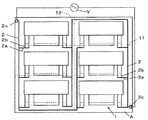
図1及び図2は、複数の有機EL素子1が形成された多面取り用のベース基板Aを示す図である。 1 and 2 are diagrams showing a multi-sided base substrate A on which a plurality of organic EL elements 1 are formed.
ベース基板Aは、長方形形状の透明ガラス材からなり、電気絶縁性の基板である。ベース基板A上には、複数の有機EL素子1と、第一の導通ライン2と、第二の導通ライン3とが形成されている。また、ベース基板A上には各有機EL素子1を気密的に覆う封止部材が配設されるが、図1及び図2においては封止部材を省略している。
The base substrate A is made of a rectangular transparent glass material and is an electrically insulating substrate. On the base substrate A, a plurality of organic EL elements 1, a
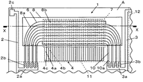
有機EL素子1は、図2及び図3に示すように、ライン状に複数形成される陽極(電極)4と、絶縁層5と、隔壁部6と、有機層7と、ライン状に複数形成される陰極(電極)8と、から主に構成され、各陽極4と各陰極8とが交差するとともに有機層7を陽極4と陰極8とで挟持する個所からなる複数の発光部(画素)を備えるいわゆるドットマトリクス型の有機EL素子である。また、有機EL素子1は、図3に示すように、封止部材9によって気密的に覆われている。
As shown in FIGS. 2 and 3, the organic EL element 1 includes a plurality of anodes (electrodes) 4 formed in a line, an
陽極4は、ITO等の透光性の導電材料からなり、蒸着法やスパッタリング法等の手段によってベース基板A上に前記導電材料を層状に形成した後、フォトリソグラフィー法等によって互いに略平行となるようにライン状に複数形成される。陽極4は、陽極配線部4a及び陽極部4bを有しており、陽極配線部4aは終端部に陽極端子部4cを備える。
The anode 4 is made of a light-transmitting conductive material such as ITO. After the conductive material is formed in layers on the base substrate A by means such as vapor deposition or sputtering, the anodes 4 are substantially parallel to each other by photolithography or the like. Thus, a plurality of lines are formed. The anode 4 has an
絶縁層5は、例えばポリイミド系の電気絶縁性材料から構成され、陽極4と陰極8との間に位置するように陽極4上に形成され、両電極4,8の短絡を防止するとともに、有機EL素子1の輪郭を明確にするものである。
The
隔壁部6は、例えばフェノール系の電気絶縁性材料からなり、絶縁層5上に形成される。隔壁部6は、その断面が絶縁層5に対して逆テーパー形状等のオーバーハング形状となるようにフォトリソグラフィー法等の手段によって形成されるものである。また、隔壁部6は、陽極4と直交する方向に等間隔にて複数形成される。隔壁部6は、その上方から蒸着法やスパッタリング法等によって有機層7及び陰極8となる金属膜を形成する場合にオーバーハング形状によって有機層7及び前記金属膜が段切れを起こす構造を得るものである。
The
有機層7は、陽極4上に形成されるものであり、少なくとも発光層を有するものである。なお、本実施形態においては、有機層7は、正孔注入層,正孔輸送層,発光層及び電子輸送層を蒸着法やスパッタリング法等の手段によって順次積層形成してなるものである。なお、有機層7は、陽極4及び隔壁部6上に形成されるものであるが、隔壁部6によって段切れが生じ隔壁部6の上面に積層されるものがある。
The organic layer 7 is formed on the anode 4 and has at least a light emitting layer. In the present embodiment, the organic layer 7 is formed by sequentially laminating a hole injection layer, a hole transport layer, a light emitting layer, and an electron transport layer by means of vapor deposition or sputtering. The organic layer 7 is formed on the anode 4 and the
陰極8は、アルミニウム(Al)やマグネシウム銀(Mg:Ag)等の陽極4よりも導電率が高い金属性導電材料をスパッタリング法や蒸着法等の手段によりライン状に複数形成されるものであり、前記導電材料にて形成される金属膜が有機層7と同様に隔壁部6によって段切れが生じ、有機層7上に積層されるものと隔壁部6上に積層されるものとに区分けされ、円弧状の陰極配線部8a及び陽極4の陽極部4bに略直角に交わる(交差する)陰極部8bが形成される。また、陰極配線部8aは接続配線部10に電気的に接続されている。接続配線部10は、陽極4とともに形成されるものであり、同一材料のITOからなるものである。また、接続配線部10は、終端部に陰極端子部10aが形成されている。
The
封止部材9は、例えばガラス材料からなる平板部材であり、各有機EL素子1を収納する凹部9aと、この凹部9aの全周を取り巻くように形成される接合部9bとを備えおり、接着剤9cを介してベース基板A上に配設される。
The sealing
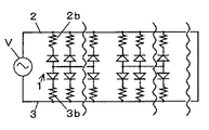
第一の導通ライン2は、陽極4と同一材料であるITO等の導電材料からなり、有機ELパネルの製造工程におけるエージング処理用あるいは検査用の交流電源(電源)Vと各有機EL素子1の複数の各陰極8からなる各第一の陰極群とを第一の接続部2aを介して電気的に一括接続するための部材であって、交流電源Vから供給される電圧を前記第一の陰極群に印加するものである。第一の接続部2aは前記各第一の陰極群に接続される接続配線部10及び陰極端子部10aに連続して設けられる接続ラインであり、末端が第一の導通ライン2と電気的に接続されている。また、第一の接続部2aには第一の導通ライン2から前記各第一の陰極群に印加される電圧を調整し、各有機EL素子1の素子破壊を防止するための第一の抵抗部2bが設けられている。また、第一の導通ライン2には、交流電源Vと電気的に接続するための第一の端子2cが設けられている。なお、第一の導通ライン2は導電材料からなるものであればよく、クロム(Cr)やアルミニウム(Al)からなるものであってもよい。
The
第二の導通ライン3は、陽極4と同一材料であるITO等の導電材料からなり、交流電源Vと各有機EL素子1の前記第一の陰極群に含まれない他の複数の各陰極8からなる各第二の陰極群とを第二の接続部3aを介して電気的に一括接続するための部材であって、第一の導通ライン2とは電気的に分断されるように形成され、交流電源Vから供給される電圧を前記各第二の陰極群に印加するものである。第二の接続部3aは、前記各第二の陰極群に接続される接続配線部10及び陰極端子部10aに連続して設けられる接続ラインであり、末端が第二の導通ライン3と電気的に接続されている。また、第二の接続部3aには第二の導通ライン3から前記各第二の陰極群に印加される電圧を調整し、各有機EL素子1の素子破壊を防止するための第二の抵抗部3bが設けられている。また、第一の導通ライン2には、交流電源Vと電気的に接続するための第二の端子3cが設けられている。なお、第二の導通ライン3は導電材料からなるものであればよく、クロム(Cr)やアルミニウム(Al)からなるものであってもよい。
The second
次に、ベース基板Aを用いた有機ELパネルの製造方法を説明する。 Next, a method for manufacturing an organic EL panel using the base substrate A will be described.
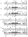
先ず、蒸着法やスパッタリング法等の手段によって支持基板1上に透光性の前記導電材料を層状に形成した後、フォトリソグラフィー法等によって第一,第二の導通ライン2,3及び陽極4をベース基板A上に形成する(図4(a)参照)。そして、陽極4の陽極部4bに対応するように絶縁層5,隔壁部6及び有機層7を積層形成し(図4(b)参照)、さらに、有機層7上に陰極6を積層形成して、各有機EL素子1を得る(図4(c)参照)。第一,第二の導通ライン2,3は有機EL素子1を構成する部材である陽極4と同材料によって形成されることで陽極4と同工程で形成することができ、多面取り基板Aの製造工程を簡素化することができる。
First, after forming the translucent conductive material in a layer form on the support substrate 1 by means such as vapor deposition or sputtering, the first and second
そして、各有機EL素子1を収納する各凹部9aと、この各凹部9aの周縁を取り囲むように設けられベース基板Aと接合するための各接合部9bとを備える封止部材7を用意し、紫外線硬化性の接着剤9cを介してベース基板A上に配設固定する(図4(d)参照)。これにより有機ELパネルを複数有する多面取り基板Aが得られる。
And preparing the sealing member 7 provided with each recessed
次に、第一,第二の導通ライン2,3と交流電源Vとを接続して第一,第二の導通ライン2,3間に所定の交流電圧を所定時間印加して有機EL素子1の欠陥部分を除去するとともに発光輝度の経時変化を抑制して素子特性を安定させるエージング処理を行う。図5は、第一,第二の導通ライン2,3と交流電源Vとを接続した際の等価回路を示している。このとき、第一の導通ライン2は各陰極8の前記各第一の陰極群と接続され、また、第二の通電ライン3は各陰極8の前記各第二の陰極群と接続されるため、電圧の印加に対して各有機EL素子1の前記発光部のうち前記各第一,第二の陰極群の一方を含む前記発光部においてはダイオード特性に対して順方向であるが他方は逆方向となるので各有機EL素子1には電流が流れにくく、各有機EL素子1が欠陥部分のない正常な状態である場合には、各有機EL素子1は発光しない。したがって、発光によって各有機EL素子1を構成する有機材料を劣化させることなくエージング処理を行うことが可能となる。また、各有機EL素子1に欠陥部分がある場合は、有機EL素子1にリーク電流が流れて有機EL素子1が部分的に発光する。そのため、各有機EL素子1が発光するか否かによって各有機EL素子1の良否を検査することが可能となっている。なお、電圧の印加によって有機EL素子1の欠陥部分が除去されると有機EL素子1は正常な状態となり発光しなくなる。また、前記各第一,第二の陰極群には交流電圧が印加されるため、周期的に第一,第二の通電ライン2,3に印加される電圧の電位が逆転し、各有機EL素子1の前記各第一,第二の陰極群の何れに対応する個所に欠陥部分がある場合であっても、電源の接続や電圧の電位を切り換えることなく有機EL素子1の良否を検査することが可能となる。なお、有機EL素子1の良否を判別する検査工程はエージング処理と同時に行ってもよいし、また、エージング処理後に行うものであってもよい。
Next, the first and second
前記エージング処理及び検査後、ベース基板Aにおいて、陰極端子部10aと第一,第二の抵抗部2b,3bとの境界に対応するベース基板Aの第一の境界部11(図1中、横方向)及びこの第一の境界部11と直交する第二の境界部12(図1中、縦方向)と、封止部材9とをスクライブ法等の手段によって切断する。(図4(e)参照)。このとき、第一,第二の導通ライン2,3はそれぞれ前記各第一,第二の陰極群から切断される。なお、封止部材9は、個々の有機ELパネルPが得られた状態で異方性導電膜等の接続部材を介してフレキシブルプリント配線(図示しない)と電気的に接続可能にするため陽極4及び接続配線部10から引き出し形成された陽極端子部4c及び陰極端子部10aを露出させる第二の凹部(図示しない)が形成されており、上述の切断工程において前記第二の凹部を切断し、陽極端子部4c及び陰極端子部10aを露出させる。
After the aging treatment and inspection, in the base substrate A, the
以上の工程によって、個々の有機ELパネルPが得られる。 Through the above steps, individual organic EL panels P are obtained.
かかる有機ELパネルPの製造方法は、分割された各陰極8のうちの前記各第一の陰極群を第一の導通ライン2に接続するとともに他の陰極8である前記第二の陰極群を第二の導通ライン3に接続し、第一の導通ライン2を交流電源Vの一端に接続するとともに第二の導通ライン3を交流電源Vの他端に接続して第一,第二の導通ライン2,3間に所定時間電圧を印加する工程を少なくとも含むものである。また、ベース基板A上に第一,第二の導通ライン2,3を形成するものである。また、また、ベース基板Aを切断する際に、第一,第二の導通ライン2,3を陰極8から切断するものである。また、交流電源Vによって、第一,第二の導通ライン2,3間に交流電圧を印加するものである。
The manufacturing method of the organic EL panel P includes connecting the first cathode group of the divided
したがって、従来のエージング処理と比較して、一方の電極である陰極8にのみ第一,第二の導通ライン2,3が接続されるため、他方の電極である陽極4に接続する接続ラインの数を低減させることができ、より簡素な構成でエージング処理を行うことが可能となる。また、ベース基板A上に第一,第二の導通ライン2,3を形成し、複数の有機EL素子1の各陰極8と接続することによって複数の導通ラインを設けることが不要となり、単一の第一,第二の導通ライン2,3と交流電源Vとを接続することで複数の有機EL素子1のエージング処理を一括して行うことができ、エージング処理における作業効率を向上させることができる。また、第一の導通ライン2は各陰極8の前記各第一の陰極群と接続され、また、第二の通電ライン3は各陰極8の前記各第二の陰極群と接続されるため、電圧の印加に対して各有機EL素子1の前記発光部のうち前記各第一,第二の陰極群の一方を含む前記発光部においてはダイオード特性に対して順方向であるが他方は逆方向となるので有機EL素子1に電流が流れにくく有機EL素子1が正常な状態においては発光しないことから、発光によって各有機EL素子1を構成する有機材料を劣化させることなくエージング処理を行うことが可能となり、有機EL素子1の発光品質を向上させることができる。
Therefore, compared with the conventional aging treatment, the first and second
また、かかる有機ELパネルPの製造方法は、分割された各陰極8のうちの複数である前記各第一の陰極群を単一の第一の導通ライン2に接続するとともに他の陰極8である前記第二の陰極群を単一の第二の導通ライン3に接続し、第一の導通ライン2を交流電源Vの一端に接続するとともに第二の導通ライン3を交流電源Vの他端に接続して第一,第二の導通ライン2,3間に電圧を印加し、各有機EL素子1の発光の有無によって良否を判別する検査工程を含むものである。
In addition, in the method of manufacturing the organic EL panel P, the first cathode group, which is a plurality of the divided
したがって、分割された陰極8のうちの複数である前記第一の陰極群が単一の第一の導通ライン2に接続され、また、他の陰極8である前記第二の陰極群が単一の第二の導通ライン3に接続されることから、導通ラインの接続を切り換えることなく有機ELパネルPの備えられる有機EL素子1の良否を判別することができ、有機ELパネルの検査工程における作業効率を向上させることが可能となる。
Therefore, the first cathode group, which is a plurality of the divided
また、交流電源Vによって、第一,第二の導通ライン2,3間に交流電圧を印加することによって、周期的に第一,第二の通電ライン2,3に印加される電圧の電位が逆転し、各有機EL素子1の前記各第一,第二の陰極群の何れに対応する個所に欠陥部分がある場合であっても、電源の接続や電圧の電位を切り換えることなく有機EL素子1の良否を判別することができ、有機ELパネルの検査工程における作業効率を向上させることが可能となる。
Further, by applying an AC voltage between the first and
なお、本実施形態では、第一,第二の導通ライン2,3が分割された陰極8にそれぞれ接続される構成であったが、本発明においては、第一の導通ラインが分割された陽極の一つ以上(第一の陽極群)に接続され、第二の導通ラインが他の陽極(第二の陽極群)に接続される構成であってもよい。
In the present embodiment, the first and second
また、本実施形態では、ドットマトリックス型の有機EL素子1を備える有機ELパネルPの製造方法について説明したが、本発明はこれに限定されることはなく、例えばセグメント型の有機EL素子において少なくとも一方の電極を支持基板上に複数形成してなる有機ELパネルについても適用可能である。 Moreover, although this embodiment demonstrated the manufacturing method of the organic electroluminescent panel P provided with the dot matrix type organic electroluminescent element 1, this invention is not limited to this, For example, in a segment type organic electroluminescent element, at least The present invention can also be applied to an organic EL panel in which a plurality of electrodes are formed on a support substrate.
A ベース基板
P 有機ELパネル
1 有機EL素子
2 第一の導通ライン
3 第二の導通ライン
4 陽極
5 絶縁層
6 リブ
7 有機層
8 陰極
9 封止部材
A base substrate P organic EL panel 1
Claims (11)
複数に分割された一方の電極のうちの1つ以上を第一の導通ラインに接続するとともに他の前記一方の電極を第二の導通ラインに接続し、前記第一の導通ラインを所定の電源の一端に接続するとともに前記第二の導通ラインを前記電源の他端に接続して前記第一,第二の導通ライン間に所定時間電圧を印加する工程を少なくとも含むことを特徴とする有機ELパネルの製造方法。 A method for producing an organic EL panel, in which an organic EL element formed by sandwiching at least an organic layer having a light emitting layer between a pair of electrodes is formed on a substrate,
One or more of one of the divided electrodes are connected to the first conduction line and the other one electrode is connected to the second conduction line, and the first conduction line is connected to a predetermined power source. And connecting the second conductive line to the other end of the power source and applying a voltage for a predetermined time between the first and second conductive lines. Panel manufacturing method.
複数に分割された各一方の電極のうちの1つ以上を第一の導通ラインに接続するとともに他の前記各一方の電極を第二の導通ラインに接続し、前記第一の導通ラインを所定の電源の一端に接続するとともに前記第二の導通ラインを前記電源の他端に接続して前記第一,第二の導通ライン間に所定時間電圧を印加する工程を少なくとも含むことを特徴とする有機ELパネルの製造方法。 A plurality of organic EL elements each having an organic layer having at least a light-emitting layer sandwiched between a pair of electrodes are formed on a base substrate, and the base substrate is cut according to each of the organic EL elements, and each organic EL panel An organic EL panel manufacturing method for obtaining
One or more of each of the divided electrodes are connected to the first conductive line and the other one electrode is connected to the second conductive line, and the first conductive line is set to a predetermined value. And connecting the second conductive line to the other end of the power supply and applying a voltage for a predetermined time between the first and second conductive lines. Manufacturing method of organic EL panel.
複数に分割された一方の電極のうちの1つ以上を第一の導通ラインに接続するとともに他の前記一方の電極を第二の導通ラインに接続し、前記第一の導通ラインを所定の電源の一端に接続するとともに前記第二の導通ラインを前記電源の他端に接続して前記第一,第二の導通ライン間に電圧を印加し、前記有機EL素子の発光の有無によって良否を判別する検査工程を少なくとも含むことを特徴とする有機ELパネルの製造方法。 A method for producing an organic EL panel, in which an organic EL element formed by sandwiching at least an organic layer having a light emitting layer between a pair of electrodes is formed on a substrate,
One or more of one of the divided electrodes are connected to the first conduction line and the other one electrode is connected to the second conduction line, and the first conduction line is connected to a predetermined power source. And connecting the second conductive line to the other end of the power source, applying a voltage between the first and second conductive lines, and determining whether the organic EL element emits light or not. The manufacturing method of the organic electroluminescent panel characterized by including the inspection process to perform at least.
複数に分割された各一方の電極のうちの1つ以上を第一の導通ラインに接続するとともに他の前記各一方の電極を第二の導通ラインに接続し、前記第一の導通ラインを所定の電源の一端に接続するとともに前記第二の導通ラインを前記電源の他端に接続して前記第一,第二の導通ライン間に電圧を印加し、各前記有機EL素子の発光の有無によって良否を判別する検査工程を少なくとも含むことを特徴とする有機ELパネルの製造方法。 A method for producing an organic EL panel, in which a plurality of organic EL elements each having an organic layer having at least a light emitting layer sandwiched between a pair of electrodes are formed on a base substrate,
One or more of each of the divided electrodes are connected to the first conductive line and the other one electrode is connected to the second conductive line, and the first conductive line is set to a predetermined value. The second conductive line is connected to the other end of the power source and a voltage is applied between the first and second conductive lines, depending on whether each organic EL element emits light. A method for manufacturing an organic EL panel, comprising at least an inspection step for determining pass / fail.
Priority Applications (1)
| Application Number | Priority Date | Filing Date | Title |
|---|---|---|---|
| JP2004102985A JP4666247B2 (en) | 2004-03-31 | 2004-03-31 | Manufacturing method of organic EL panel |
Applications Claiming Priority (1)
| Application Number | Priority Date | Filing Date | Title |
|---|---|---|---|
| JP2004102985A JP4666247B2 (en) | 2004-03-31 | 2004-03-31 | Manufacturing method of organic EL panel |
Publications (2)
| Publication Number | Publication Date |
|---|---|
| JP2005293875A true JP2005293875A (en) | 2005-10-20 |
| JP4666247B2 JP4666247B2 (en) | 2011-04-06 |
Family
ID=35326599
Family Applications (1)
| Application Number | Title | Priority Date | Filing Date |
|---|---|---|---|
| JP2004102985A Expired - Fee Related JP4666247B2 (en) | 2004-03-31 | 2004-03-31 | Manufacturing method of organic EL panel |
Country Status (1)
| Country | Link |
|---|---|
| JP (1) | JP4666247B2 (en) |
Cited By (2)
| Publication number | Priority date | Publication date | Assignee | Title |
|---|---|---|---|---|
| US8845379B2 (en) | 2010-06-02 | 2014-09-30 | Nec Lighting, Ltd. | Manufacturing method for organic EL lighting device |
| WO2015079718A1 (en) * | 2013-11-28 | 2015-06-04 | パイオニア株式会社 | Light emitting device |
Citations (3)
| Publication number | Priority date | Publication date | Assignee | Title |
|---|---|---|---|---|
| JP2000200053A (en) * | 1999-01-07 | 2000-07-18 | Futaba Corp | Method for manufacturing display element substrate and display element substrate |
| JP2003017260A (en) * | 2001-06-29 | 2003-01-17 | Toyota Motor Corp | Organic EL element inspection method |
| JP2003282249A (en) * | 2002-03-22 | 2003-10-03 | Nippon Seiki Co Ltd | Organic el panel and its manufacturing method |
-
2004
- 2004-03-31 JP JP2004102985A patent/JP4666247B2/en not_active Expired - Fee Related
Patent Citations (3)
| Publication number | Priority date | Publication date | Assignee | Title |
|---|---|---|---|---|
| JP2000200053A (en) * | 1999-01-07 | 2000-07-18 | Futaba Corp | Method for manufacturing display element substrate and display element substrate |
| JP2003017260A (en) * | 2001-06-29 | 2003-01-17 | Toyota Motor Corp | Organic EL element inspection method |
| JP2003282249A (en) * | 2002-03-22 | 2003-10-03 | Nippon Seiki Co Ltd | Organic el panel and its manufacturing method |
Cited By (4)
| Publication number | Priority date | Publication date | Assignee | Title |
|---|---|---|---|---|
| US8845379B2 (en) | 2010-06-02 | 2014-09-30 | Nec Lighting, Ltd. | Manufacturing method for organic EL lighting device |
| US9196875B2 (en) | 2010-06-02 | 2015-11-24 | Nec Lighting, Ltd. | Manufacturing method for organic EL lighting device |
| JP5911105B2 (en) * | 2010-06-02 | 2016-04-27 | Necライティング株式会社 | Organic EL lighting device repair method |
| WO2015079718A1 (en) * | 2013-11-28 | 2015-06-04 | パイオニア株式会社 | Light emitting device |
Also Published As
| Publication number | Publication date |
|---|---|
| JP4666247B2 (en) | 2011-04-06 |
Similar Documents
| Publication | Publication Date | Title |
|---|---|---|
| JP2005116507A (en) | Flat panel display device and manufacturing method thereof | |
| JP2003257667A (en) | Organic electroluminescent device and method of manufacturing the same | |
| JP5184652B2 (en) | Electroluminescent device with improved brightness uniformity | |
| JP2010032741A5 (en) | ||
| KR20050022993A (en) | FPD with compensated IR drop | |
| CN105161517A (en) | Restoration method, restoration device and preparation method of array substrate | |
| JPWO2001078463A1 (en) | Organic EL display device | |
| KR20130061543A (en) | Organic light emitting device capable of reducing leakage current between pixels | |
| JP3606309B2 (en) | Organic thin film light emitting display | |
| JP2001196191A (en) | Organic thin-film light emitting display and method of manufacturing the same | |
| US8022614B2 (en) | Display panel and method for manufacturing the same | |
| JP3633841B2 (en) | Repair method of organic thin film light emitting display | |
| JP4666247B2 (en) | Manufacturing method of organic EL panel | |
| WO2012032661A1 (en) | Organic el panel | |
| CN106653807B (en) | Surface-mounted OLED display unit device, display screen and manufacturing method thereof | |
| JP2003208108A (en) | Display device and method of manufacturing the same | |
| JP2004063407A (en) | Multiple arrangement substrate and its manufacturing method | |
| JP2008243396A (en) | Planar light emitting device | |
| JP4499490B2 (en) | Organic EL display device substrate and organic EL display device | |
| JP5263605B2 (en) | Mother panel and organic EL panel manufacturing method | |
| JP2007141536A (en) | Manufacturing method of organic electroluminescent panel | |
| JP4721049B2 (en) | Manufacturing method of organic EL panel | |
| JP2004192925A (en) | Organic el display panel and its inspection method | |
| JP2003092190A (en) | Organic electroluminescent device and method of manufacturing the same | |
| JP2008311094A (en) | Organic EL panel |
Legal Events
| Date | Code | Title | Description |
|---|---|---|---|
| A621 | Written request for application examination |
Free format text: JAPANESE INTERMEDIATE CODE: A621 Effective date: 20070119 |
|
| A977 | Report on retrieval |
Free format text: JAPANESE INTERMEDIATE CODE: A971007 Effective date: 20090819 |
|
| A131 | Notification of reasons for refusal |
Free format text: JAPANESE INTERMEDIATE CODE: A131 Effective date: 20090824 |
|
| A521 | Request for written amendment filed |
Free format text: JAPANESE INTERMEDIATE CODE: A523 Effective date: 20091006 |
|
| A131 | Notification of reasons for refusal |
Free format text: JAPANESE INTERMEDIATE CODE: A131 Effective date: 20100818 |
|
| TRDD | Decision of grant or rejection written | ||
| A01 | Written decision to grant a patent or to grant a registration (utility model) |
Free format text: JAPANESE INTERMEDIATE CODE: A01 Effective date: 20101217 |
|
| A01 | Written decision to grant a patent or to grant a registration (utility model) |
Free format text: JAPANESE INTERMEDIATE CODE: A01 |
|
| A61 | First payment of annual fees (during grant procedure) |
Free format text: JAPANESE INTERMEDIATE CODE: A61 Effective date: 20101230 |
|
| FPAY | Renewal fee payment (event date is renewal date of database) |
Free format text: PAYMENT UNTIL: 20140121 Year of fee payment: 3 |
|
| R150 | Certificate of patent or registration of utility model |
Free format text: JAPANESE INTERMEDIATE CODE: R150 |
|
| LAPS | Cancellation because of no payment of annual fees |