JP2005293609A - Initialization method - Google Patents
Initialization method Download PDFInfo
- Publication number
- JP2005293609A JP2005293609A JP2005139979A JP2005139979A JP2005293609A JP 2005293609 A JP2005293609 A JP 2005293609A JP 2005139979 A JP2005139979 A JP 2005139979A JP 2005139979 A JP2005139979 A JP 2005139979A JP 2005293609 A JP2005293609 A JP 2005293609A
- Authority
- JP
- Japan
- Prior art keywords
- address
- processor
- reset signal
- register
- control unit
- Prior art date
- Legal status (The legal status is an assumption and is not a legal conclusion. Google has not performed a legal analysis and makes no representation as to the accuracy of the status listed.)
- Pending
Links
Images


Landscapes
- Stored Programmes (AREA)
Abstract
【課題】 プロセッサのソフトウェア的な初期化処理をより高速に行うことができるようにする。
【解決手段】 マスタープロセッサとスレーブプロセッサとの間で通信を行うシステムにおいて、リセット信号に応じて、第1の初期化処理を行った後で初期化プログラムを使用してソフトウェア的な第2の初期化処理を行う初期化方法が提供される。マスタープロセッサが、リセット信号の種類に基づいて、初期化プログラムがローカルメモリ(6)又は外部メモリ(9)の何れにあるかを設定し、スレーブプロセッサは、選択されたローカルメモリ又は外部メモリから初期化プログラムを読み出す。
【選択図】 図1
PROBLEM TO BE SOLVED: To perform a software initialization process of a processor at higher speed.
In a system that performs communication between a master processor and a slave processor, a software-based second initial operation is performed using an initialization program after performing a first initialization process in response to a reset signal. An initialization method for performing the initialization process is provided. The master processor sets whether the initialization program is in the local memory (6) or the external memory (9) based on the type of the reset signal, and the slave processor initializes from the selected local memory or external memory. Read the program.
[Selection] Figure 1
Description
本発明は、初期化方法に関する。 The present invention relates to an initialization method.
ある装置に備えられたマイクロプロセッサは、装置の電源が投入されると、外部から与えられるリセット信号に応じてプロセッサ内部を初期化するリセット動作を行う。このリセット動作では、プロセッサ内部に備えられた記憶素子の記憶内容を初期化するハードウェア的な初期化処理の後、外部メモリから初期化処理用のプログラムを読み込んで実行することにより、種々のアプリケーションプログラムを実行可能な状態に設定するソフトウェア的な初期化処理が行われる。 When a power supply of a device is turned on, a microprocessor provided in a device performs a reset operation for initializing the inside of the processor according to a reset signal given from the outside. In this reset operation, various initialization applications are executed by reading and executing an initialization process program from an external memory after a hardware initialization process for initializing the storage contents of a storage element provided in the processor. Software initialization processing for setting the program to an executable state is performed.
上記ハードウェア的な初期化処理は、リセット信号のアサートを契機として行われる。また、上記ソフトウェア的な初期化処理は、リセット信号のネゲートを契機として、リセットベクタで指定されるアドレスから初期化処理用プログラムの命令をフェッチすることによって行われる。通常、この初期化処理用プログラムは、プロセッサの外部にバスを介して接続されたリード・オンリ・メモリ(以下、ROM)に格納されている。 The hardware initialization process is performed in response to assertion of a reset signal. The software initialization process is performed by fetching the instruction of the initialization process program from the address specified by the reset vector, triggered by the negation of the reset signal. Normally, this initialization processing program is stored in a read-only memory (hereinafter referred to as ROM) connected to the outside of the processor via a bus.
すなわち、ソフトウェア的な初期化処理では、プロセッサがバスを介してROMに読み出し要求アドレスを与えることで、初期化処理用プログラムの命令列がROMから順次読み出されてバスを介してプロセッサに供給される。これを受け取ったプロセッサは、供給された命令に従って、プロセッサ内部に備えられている各種設定用レジスタにシステムに応じた適当な値を設定することにより、アプリケーションプログラムを実行可能な環境を整備する。 That is, in software initialization processing, the processor gives a read request address to the ROM via the bus, so that the instruction sequence of the initialization processing program is sequentially read from the ROM and supplied to the processor via the bus. The Upon receiving this, the processor sets an appropriate value according to the system in various setting registers provided in the processor according to the supplied instruction, thereby preparing an environment in which the application program can be executed.
ところで、このようなリセット動作を行うプロセッサを共有バスに複数個接続し、そのうちの1つをマスタープロセッサ、その他をスレーブプロセッサとして機能させるようにしたマルチプロセッサを構成するシステムが存在する。このようなマルチプロセッサシステム全体をリセットするためには、全てのプロセッサにおいてリセット動作を行う必要がある。 By the way, there is a system that constitutes a multiprocessor in which a plurality of processors that perform such a reset operation are connected to a shared bus, and one of them functions as a master processor and the other as a slave processor. In order to reset such an entire multiprocessor system, it is necessary to perform a reset operation in all the processors.
そのために、まず全てのプロセッサに対してリセット信号がアサートされ、全てのプロセッサにおいてハードウェア的な初期化処理が行われる。そして、プロセッサ内部の記憶素子の記憶内容を初期化するために必要十分な時間だけリセット信号がアサートされた後、このリセット信号は各プロセッサに対してネゲートされる。 For this purpose, first, a reset signal is asserted to all processors, and hardware initialization processing is performed in all processors. Then, after a reset signal is asserted for a time necessary and sufficient for initializing the storage contents of the storage elements in the processor, the reset signal is negated for each processor.
このリセット信号のネゲートを契機として、各プロセッサは続いてソフトウェア的な初期化処理を行うために、リセットベクタで指示されるアドレスに従ってROMに対するアクセスを一斉に開始しようとする。しかし、共有バス上に接続されたROMに対して複数のプロセッサが同時にアクセスすることはできない。そのため、各プロセッサは、共有バスのアービトレーション(バス調停)を介してROMに順番にアクセスし、ソフトウェア的な初期化処理のために必要なプログラムの命令列を順に読み出すことになる。 In response to the negation of the reset signal, the respective processors attempt to start access to the ROM all at once according to the address indicated by the reset vector in order to perform software initialization processing. However, a plurality of processors cannot access the ROM connected on the shared bus at the same time. For this reason, each processor sequentially accesses the ROM via arbitration (bus arbitration) of the shared bus, and sequentially reads out an instruction sequence of a program necessary for software initialization processing.
また、上述のようなリセット動作を行うプロセッサを組み込んだシステムにおいて、電源投入後においてもプロセッサが動作していない状態では、当該プロセッサでのクロック供給を停止することにより、消費電力の低減化を図ったシステムも提案されている。例えば、上述のようなマルチプロセッサにより構成されるシステムでは、マスタープロセッサが動作してスレーブプロセッサが動作していない状態が存在するが、この場合にはスレーブプロセッサでのクロック供給を停止することにより、低消費電力化を図っている。 Also, in a system incorporating a processor that performs the reset operation as described above, when the processor is not operating even after the power is turned on, the clock supply to the processor is stopped to reduce power consumption. A system has also been proposed. For example, in a system composed of multiprocessors as described above, there is a state in which the master processor is operating and the slave processor is not operating. In this case, by stopping the clock supply in the slave processor, Low power consumption is achieved.
プロセッサのクロック供給が停止されている状態で、その後そのプロセッサを使用する状態が発生したときは、再びクロックが供給されてプロセッサの起動が行われる。このとき、再起動されるプロセッサでは、リセット信号のアサートに応じてハードウェア的な初期化処理を行った後、リセット信号のネゲートに応じてバスを介してROMにアクセスし、必要な初期化処理用プログラムの命令列を読み込んでソフトウェア的な初期化処理を実行することになる。 When the processor clock supply is stopped and the processor is subsequently used, the clock is supplied again to start the processor. At this time, the restarted processor performs a hardware initialization process in response to the assertion of the reset signal, and then accesses the ROM via the bus in accordance with the negation of the reset signal to perform the necessary initialization process. The instruction sequence of the computer program is read and software initialization processing is executed.
しかしながら、上記従来のシステムにおいては、ハードウェア的な初期化処理の後に続いて行われるソフトウェア的な初期化処理では、その初期化処理に必要なプログラムを、バスを介して低速なメモリデバイスであるROMにアクセスして取得しなければならず、そのリセット動作に多くの時間がかかっていた。 However, in the above-described conventional system, in the software initialization process performed after the hardware initialization process, a program necessary for the initialization process is a low-speed memory device via the bus. The ROM had to be accessed and acquired, and the reset operation took a lot of time.
特に、低消費電力化のためにプロセッサのクロック供給を一時的に停止するようにしたシステムにおいて、プロセッサの停止と起動とが頻繁に行われると、低速なROMへのアクセスがプロセッサ起動の度に実行されるため、システムの起動待ちという無駄な時間が増大するという問題があった。 In particular, in a system in which the clock supply of the processor is temporarily stopped to reduce power consumption, if the processor is frequently stopped and started, access to the low-speed ROM is performed each time the processor is started. Since this is executed, there is a problem in that useless time for waiting for the system to start increases.
また、複数のプロセッサが共有バス上に接続されたマルチプロセッサシステムにおいては、それぞれのプロセッサが実行する初期化処理用のプログラムを記憶したROMが共有バスに接続されているため、各プロセッサからROMへのアクセスが競合した場合は、バス調停が行われて各プロセッサが低速なROMに順次アクセスすることになる。そのため、全てのプロセッサの初期化に要する時間が大幅に増大してしまうという問題があった。 Further, in a multiprocessor system in which a plurality of processors are connected on a shared bus, a ROM storing an initialization process program executed by each processor is connected to the shared bus. When the accesses conflict, bus arbitration is performed, and each processor sequentially accesses the low-speed ROM. Therefore, there is a problem that the time required for initialization of all the processors is greatly increased.
さらに、マルチプロセッサシステムでは、それぞれのプロセッサには異なる役割が与えられるのが通常であり、ソフトウェア的な初期化処理の内容もそれぞれ異なるものとなる。そのため、初期化処理のために使用するプログラムもそれぞれのプロセッサ毎に異なるものとなる。したがって、ROM内に格納された異なるプログラムのうち、どのプログラムをどのプロセッサが実行するのかを判別する機構が必要となり、システムの構成が煩雑になるという問題があった。 Furthermore, in a multiprocessor system, each processor is usually assigned a different role, and the contents of software initialization processing are also different. For this reason, the program used for the initialization process is different for each processor. Therefore, there is a problem that a mechanism for determining which processor executes which program among the different programs stored in the ROM is required, resulting in a complicated system configuration.
本発明は、このような問題を解決するために成されたものであり、プロセッサのソフトウェア的な初期化処理をより高速に行うことができるようにすることを目的とする。
また、本発明は、プロセッサのソフトウェア的な初期化処理を行うための機構をより簡素化することができるようにすることをも目的とする。
The present invention has been made to solve such a problem, and an object of the present invention is to enable a software initialization process of a processor to be performed at a higher speed.
Another object of the present invention is to make it possible to further simplify a mechanism for performing software initialization processing of a processor.
本発明の初期化方法は、マスタープロセッサとスレーブプロセッサとの間で通信を行うシステムにおいて、リセット信号に応じて、第1の初期化処理を行った後で初期化プログラムを使用してソフトウェア的な第2の初期化処理を行う初期化方法であって、前記マスタープロセッサが、前記リセット信号の種類に基づいて、初期化プログラムがローカルメモリ又は外部メモリの何れにあるかを設定し、前記スレーブプロセッサは、前記選択されたローカルメモリ又は外部メモリから初期化プログラムを読み出すことを特徴とする。 In the initialization method of the present invention, in a system in which communication is performed between a master processor and a slave processor, after performing a first initialization process in response to a reset signal, an initialization program is used to perform software-like processing. An initialization method for performing a second initialization process, wherein the master processor sets whether an initialization program is in a local memory or an external memory based on a type of the reset signal, and the slave processor Reads out the initialization program from the selected local memory or external memory.
電源投入後において内部クロックの供給が停止された後の再起動時には、高速なローカルメモリから再起動用の初期化プログラムを読み出してプロセッサの起動を行うことができ、その再起動処理を高速に行うことができる。これにより、システムの消費電力を抑制するとともにクロック停止状態からの高速な復帰を実現することができるようになる。また、マルチプロセッサシステムを構成した場合に、どのプロセッサがどのプログラムを実行するのかを判別するための機構も不要となり、システムの構成を簡素化することができる。 When restarting after the internal clock supply is stopped after the power is turned on, the initialization program for restart can be read from the high-speed local memory to start the processor, and the restart process is performed at high speed. be able to. As a result, the power consumption of the system can be suppressed and high-speed recovery from the clock stop state can be realized. Further, when a multiprocessor system is configured, a mechanism for determining which processor executes which program is not required, and the system configuration can be simplified.
以下、本発明の一実施形態を図面に基づいて説明する。
図1は、本発明によるデータ処理システムの第1の実施形態に係るプロセッサの構成例を示すブロック図である。
Hereinafter, an embodiment of the present invention will be described with reference to the drawings.
FIG. 1 is a block diagram showing a configuration example of a processor according to a first embodiment of a data processing system according to the present invention.
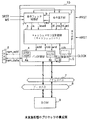
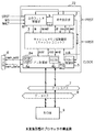
本実施形態のプロセッサ10は、メモリからプログラムの命令を読み出してフェッチする動作を制御する命令フェッチ制御部1、フェッチされた命令を解釈して実行する命令実行部2、メモリの内容のコピーを保持して高速なメモリアクセスをサポートするキャッシュメモリおよびその制御部(以下、キャッシュユニット3と略す)、ローカルなメモリであるランダム・アクセス・メモリ(RAM)6およびアドレスバス7やデータバス8などの外部バスの制御を行うバス制御部4、与えられる外部クロックCLOCKに基づいて内部クロックbck,cckの生成および分配を行うクロック制御部5を備えて構成されている。
The
外部バス7,8には、外部メモリであるROM9が接続されており、プロセッサ10のソフトウェア的な初期化処理を行うために必要な初期化プログラムがここにあらかじめ記憶されている。なお、ここでは外部メモリとしてROM9を想定しているが、これに限られない。また、RAM6は、通常はプロセッサ10のワークメモリとして使用されるものであり、必要に応じてROM9から外部バス7,8を介して初期化プログラムが転送され、格納される。
A ROM 9 which is an external memory is connected to the
なお、キャッシュユニット3内のキャッシュメモリは、プロセッサ10に接続された外部メモリの内容のコピーを保持する、高速ではあるが容量の小さなバッファメモリである。外部メモリの内容のコピーがキャッシュメモリに存在していた場合、命令実行部2に対するデータはこのキャッシュメモリから供給される。本発明に関する限り、キャッシュユニット3の有無は本質的な意味を持たないため、詳細な説明は割愛する。本実施形態では、キャッシュメモリとしては、例えばストアスルー型のものを用いるものとする。
The cache memory in the
上記命令フェッチ制御部1は、プロセッサ10が実行すべき初期化プログラムの命令が格納されているメモリのアドレスを生成し、それを要求命令アドレスiaとして命令フェッチ要求iavalと共にキャッシュユニット3に発行する。このとき、命令フェッチ制御部1は、外部から与えられるアドレス選択信号MSに基づいて、ローカルメモリであるRAM6または外部メモリであるROM9の何れかの開始アドレスを選択して要求命令アドレスiaとする。つまり、この命令フェッチ制御部1は、本発明のアドレス選択手段を備えている。
The instruction fetch control unit 1 generates an address of a memory in which an instruction of an initialization program to be executed by the
命令フェッチ制御部1から命令フェッチ要求iavalを受け取ったキャッシュユニット3は、それに伴って与えられた要求命令アドレスiaを用いて、キャッシュメモリ内に有効なエントリが存在するかどうかを検索する。ここでキャッシュヒットした場合には、キャッシュメモリから該当するデータを読み出して、それを命令データidとして命令実行部2に供給する。一方、キャッシュメモリ内に有効なエントリが存在せず、キャッシュミスが発生した場合には、命令フェッチ要求と要求アドレスaddとをバス制御部4に供給する。
The
バス制御部4は、受け取った要求アドレスaddに従って、RAM6またはROM9の何れかに対して選択的にデータの読み出しを要求する。すなわち、このバス制御部4は、RAM6のアドレス領域を指定する情報を保持するための領域指定レジスタ4aを備えており、ここには領域の先頭アドレスASRおよび領域サイズAMRの情報が保持されている。そして、キャッシュユニット3から受け取った要求アドレスaddが、この先頭アドレスASRおよび領域サイズAMRの対によって指定されるRAM6のアドレス領域に含まれているか否かに応じて、RAM6またはROM9の何れかに対してデータの読み出しを要求する。
The
図2は、上記RAM6やROM9の他に、プロセッサ10内の各種レジスタを含むシステム全体のメモリマップを示す図である。図2の例では、アドレス番号が0x0000_0000〜0x01FF_FFFFまではRAM6に割り当てられ、0xFE00_0000〜0xFF00_0000まではプロセッサ10内の各構成(命令フェッチ制御部1、命令実行部2、キャッシュメモリ3、バス制御部4およびクロック制御部5)に備えられる各種レジスタに割り当てられ、0xFF00_0000〜0xFFFF_FFFFまではROM9に割り当てられている。なお、0x01FF_FFFF〜0xFE00_0000までのアドレス番号は未使用である。
FIG. 2 is a diagram showing a memory map of the entire system including various registers in the
この図2の例に従えば、領域指定レジスタ4aの先頭アドレスASRの情報として0x0000_0000のアドレス番号が保持され、領域サイズAMRの情報として01FF_FFFFの領域サイズが保持されている。したがって、バス制御部4は、キャッシュユニット3から受け取った要求アドレスaddが0x0000_0000〜0x01FF_FFFFの範囲内に含まれていれば、アドレス線 ram_add に要求アドレスaddを載せてRAM6に対してデータの読み出しを要求する。
According to the example of FIG. 2, the address number of 0x0000_0000 is held as information of the start address ASR of the
また、バス制御部4は、受け取った要求アドレスaddが、領域指定レジスタ4a内の先頭アドレスASRおよび領域サイズAMRの対によって指定される上記0x0000_0000〜0x01FF_FFFFのアドレス領域に含まれておらず、かつ、メモリマップされたプロセッサ10内の各種レジスタの領域を表す0xFE00_0000〜0xFF00_0000のアドレス領域にも含まれていなかった場合は、アドレスバス7に要求アドレスaddを載せてROM9に対してデータの読み出しを要求する。
The
RAM6またはROM9に対して要求されたデータは、それぞれのメモリから読み出され、データ線 ram_dataまたはデータバス8を介してバス制御部4に送られてくる。このデータを受け取ったバス制御部4は、それをリードデータrddとしてキャッシュユニット3に供給する。リードデータrddを受けたキャッシュユニット3は、そのデータを命令データidとして命令実行部2に供給し、必要に応じてキャッシュメモリにこの命令データを登録する。
Data requested to the
以上のようにして命令データidの供給を受けた命令実行部2は、その命令を解釈して実行する。この実行の過程でRAM6、ROM9あるいはプロセッサ10内の各種レジスタなどに格納されたデータを参照する必要が生じた場合、命令実行部2は、要求データアドレスoaを伴ってデータフェッチ要求をキャッシュユニット3に発行する。
The
このときのデータフェッチに関して、これ以降の動作は命令フェッチの場合とほぼ同様である。ただし、メモリマップされたレジスタのアドレス領域(0xFE00_0000〜0xFF00_0000)を要求アドレスaddが指定していた場合、バス制御部4はそのレジスタの値(領域指定レジスタ4aや後述するリセットレジスタ(RSTR)4bの値)を読み出してリードデータrddとしてキャッシュユニット3に返す。また、RAM6、ROM9あるいはレジスタからバス制御部4を介してキャッシュユニット3に返されたデータは、最終的にリードデータrdとして命令実行部2に供給される。
Regarding the data fetch at this time, the subsequent operations are almost the same as in the case of the instruction fetch. However, when the request address add designates the address area (0xFE00_0000 to 0xFF00_0000) of the memory-mapped register, the
また、命令実行部2における命令実行の過程で、RAM6あるいはレジスタなどのメモリの内容を更新する必要が生じた場合には、要求データアドレスoaとライトデータwdとを伴ってデータライト要求をキャッシュユニット3に発行する。キャッシュユニット3は、キャッシュヒットした場合にはキャッシュメモリにライトデータwdを書き込むとともに、バス制御部4に対して要求アドレスaddを伴うデータライト要求とライトデータwrdとを発行する。
In the course of instruction execution in the
このデータライト要求を受け取ったバス制御部4は、受け取った要求アドレスaddが、領域指定レジスタ4a内の先頭アドレスASRおよび領域サイズAMRの対によって指定されるRAM6のアドレス領域に含まれていた場合には、アドレス線 ram_add に要求アドレスadd、データ線 ram_dataにライトデータwrdを載せてRAM6に対してデータの書き込みを要求する。また、受け取った要求アドレスaddが、領域指定レジスタ4aやリセットレジスタ4bなどのメモリマップされたレジスタのアドレス領域を指定していた場合は、バス制御部4は、その要求アドレスaddで示されるレジスタに対してライトデータwrdの書き込みを行う。
The
また、バス制御部4は、受け取った要求アドレスaddが、領域指定レジスタ4a内の先頭アドレスASRおよび領域サイズAMRの対によって指定されるRAM6のアドレス領域に含まれておらず、かつ、メモリマップされたレジスタのアドレス領域にも含まれていなかった場合は、アドレスバス7に要求アドレスadd、データバス8にライトデータwrdを載せてROM9に対してデータの書き込みを要求する。
Further, the
本実施形態のプロセッサ10は、外部から与えられるクロックCLOCKによって駆動されている。クロック制御部5は、この外部クロックCLOCKをもとに第1、第2の内部クロックbck,cckを発生する。そして、バス制御部4に対しては第1の内部クロックbckを供給し、それ以外の命令フェッチ制御部1、命令実行部2およびキャッシュユニット3には第2の内部クロックcckを供給している。
The
このクロック制御部5に対しては、内部クロックbck,cckの供給を停止させることを指示するクロック停止信号stopが命令実行部2から必要に応じて与えられる。すなわち、このプロセッサ10は、命令実行部2においてクロック停止用の命令を実行することにより、内部クロックbck,cckの供給を自ら停止させることができるようになっている。クロックの停止モードとして、2つの内部クロックbck,cckを共に停止させる第1のモードと、第2の内部クロックcckのみを停止させる第2のモードとの2つがある。
A clock stop signal stop instructing to stop the supply of the internal clocks bck and cck is supplied from the
一旦停止させたクロック供給を再開するためには、初期起動リセット信号PRST(本発明の第1のリセット信号)あるいは再起動リセット信号HRST(本発明の第2のリセット信号)の何れかをアサートする方法か、バス制御部4が備えるリセットレジスタ4bに図示しない外部バスマスタから書き込みを行い、上記再起動リセット信号HRSTあるいは次に述べるプログラムリセット信号SRSTに相当するリセット信号(起動信号wup)をバス制御部4の内部で生成してアサートする方法がある。後者の方法を採用する場合には、第1の内部クロックbckはバス制御部4に供給され続けている必要があるため、この場合は上述の第2のモードが採用される。
In order to restart the clock supply once stopped, either the initial activation reset signal PRST (first reset signal of the present invention) or the restart reset signal HRST (second reset signal of the present invention) is asserted. Or a
なお、図1中には詳細に示していないが、上記初期起動リセット信号PRSTおよび再起動リセット信号HRSTは、プロセッサ10内の各構成(命令フェッチ制御部1、命令実行部2、キャッシュユニット3、バス制御部4およびクロック制御部5)に与えられるようになっている。本実施形態では、これらのリセット信号の他に、内部クロックbck,cckの供給停止および再開とは関係なく独自にリセット動作を行うプログラムリセット信号SRST(本発明の第3のリセット信号)も用意されている。このプログラムリセット信号SRSTは、例えばデバッグを行うときなどに利用され、命令フェッチ制御部1および命令実行部2に対してのみ供給されるようになっている。
Although not shown in detail in FIG. 1, the initial start reset signal PRST and the restart reset signal HRST are the components in the processor 10 (the instruction fetch control unit 1, the
図3は、上記命令フェッチ制御部1の詳細な構成例を示す図である。図3において、要求命令アドレスiaは、命令アドレスレジスタ11に保持され、キャッシュユニット3へと供給される。プロセッサ10が順次命令を実行している状態では、次の要求命令アドレスiaとして、命令アドレスレジスタ11に保持されている現在のアドレスに対して値"16"が加算器12で加算され、その結果がセレクタ13,14にて選択されて命令アドレスレジスタ11に保持される。このインクリメント値"16"は、プロセッサ10の命令データバスのバス幅が指定されている。
FIG. 3 is a diagram showing a detailed configuration example of the instruction fetch control unit 1. In FIG. 3, the requested instruction address ia is held in the
また、プロセッサ10が分岐命令を実行した場合には、命令実行部2から分岐したことを通知する信号bがアサートされる。この場合は、次の要求命令アドレスiaとして、命令実行部2から送られてくる分岐先アドレスbadがセレクタ13にて選択されて、セレクタ14を介して命令アドレスレジスタ11に保持される。
When the
また、初期起動リセット信号PRST、再起動リセット信号HRST、プログラムリセット信号SRSTおよびリセットレジスタ4bからの起動信号wup(以下、これら4つの信号を総称して単にリセット信号と呼ぶ)によりプロセッサ10の初期化が行われている状態では、外部から与えられるアドレス選択信号MSに応じてセレクタ15により選択された何れかのアドレス(0x0000_0000または0xFF00_0000)が、上記リセット信号に応じてセレクタ14にて選択されて命令アドレスレジスタ11に保持される。
The
例えば、初期起動リセット信号PRSTが入力されるとき、つまり、装置の電源が投入されたときには、アドレス選択信号MSの値が"1"に設定され、ROM9のアドレス領域の先頭アドレスを表す固定値"0xFF00_0000"が選択されて命令アドレスレジスタ11に保持される。一方、再起動リセット信号HRSTが入力されるとき、つまり、内部クロックbck,cckの供給停止状態からクロック供給を再開するときには、アドレス選択信号MSの値が"0"に設定され、RAM6のアドレス領域の先頭アドレスを表す固定値"0x0000_0000"が選択されて命令アドレスレジスタ11に保持される。
プログラムリセット信号SRSTや起動信号wupが入力されたときも、再起動リセット信号HRSTが入力されたときと同様である。
For example, when the initial activation reset signal PRST is input, that is, when the power of the apparatus is turned on, the value of the address selection signal MS is set to “1” and a fixed value indicating the head address of the address area of the ROM 9 0xFF00_0000 "is selected and held in the
The case where the program reset signal SRST and the start signal wup are input is the same as the case where the restart reset signal HRST is input.
これにより、リセット信号がネゲートされて初期化プログラムの命令フェッチを最初に行おうとした際の要求命令アドレスiaは、ROM9の先頭アドレス"0xFF00_0000"あるいはRAM6の先頭アドレス"0x0000_0000"の何れかとなる。このように、アドレス選択信号MSにより選択動作を行うセレクタ14,15によって本発明のアドレス選択手段が構成される。
Thus, the request instruction address ia when the reset signal is negated and the instruction fetch of the initialization program is first performed is either the leading address “0xFF00_0000” of the ROM 9 or the leading address “0x0000_0000” of the
また、命令フェッチ制御ロジック16は、与えられるリセット信号に応じて、プロセッサ10の命令実行状況やキャッシュ制御部の状況等に従って命令フェッチ要求iavalの発行の可否を決定する。命令アドレスレジスタ11内に保持された要求命令アドレスiaは、キャッシュユニット3に対して命令フェッチ要求iavalがアサートされてこれが受け付けられるまでは、更新されることはない。
Further, the instruction fetch
図4は、バス制御部4の領域指定レジスタ4aを含む部分の詳細な構成例を示す図であり、アドレスおよびデータの流れを示している。図4に示すように、バス制御部4は、バスI/F21と、メモリ制御部22と、外部バス制御部23とを備えている。上記バスI/F21は、上述の領域指定レジスタ4aを有するバスコマンド制御部24と、リードデータパス25と、ライトデータパス26とを備えている。
FIG. 4 is a diagram showing a detailed configuration example of a portion including the
また、上記メモリ制御部22は、メモリ−バスI/F(MBI)27と、メモリI/F(MI)28と、メモリ−外部バスI/F(MEI)29とを備えている。また、上記外部バス制御部23は、外部バス−バスI/F(EBI)30と、外部バス−メモリI/F(EMI)31と、外部バスI/F32とを備えている。
The
以下に、命令フェッチ時におけるバス制御部4の動作を説明する。キャッシュユニット3からの命令フェッチ要求を受けたバス制御部4は、バスコマンド制御部24において、当該命令フェッチ要求と共に与えられた要求アドレスaddと、領域指定レジスタ4aにあらかじめ設定されている先頭アドレスASRおよび領域サイズAMRの値とを比較し、要求アドレスaddがRAM6のアドレス領域内のものかどうかを判定する。
The operation of the
このアドレス比較の結果、命令フェッチ要求がRAM6に対する要求であった場合、バスコマンド制御部24は、メモリ制御部22に対して命令フェッチ要求を発行する。この命令フェッチ要求をメモリ−バスI/F27で受けたメモリ制御部22は、メモリI/F28を介して接続されたRAM6をアクセスして、上記要求アドレスaddに対応する命令データを読み出す。読み出された命令データは、メモリ−バスI/F27およびリードデータパス25を介してキャッシュユニット3へと送り返され、最終的に命令実行部2へと送られる。
As a result of the address comparison, when the instruction fetch request is a request for the
一方、上記のアドレス比較の結果、命令フェッチ要求が外部バス7,8上に接続されたROM9に対する要求であった場合、バスコマンド制御部24は、外部バス制御部23に対して命令フェッチ要求を発行する。この命令フェッチ要求を外部バス−バスI/F30で受けた外部バス制御部23は、バスの調停を行い、外部バス7,8上にメモリトランザクションを発行してその応答を待つ。
On the other hand, as a result of the address comparison, if the instruction fetch request is a request for the ROM 9 connected to the
そして、外部バス7,8上のROM9から読み出された命令データが外部バス7,8に出力されると、外部バス制御部23はその命令データを外部バスI/F32を介して取り込む。こうして取り込まれた命令データは、外部バス−バスI/F30およびリードデータパス25を介してキャッシュユニット3へと送り返され、最終的に命令実行部2へと送られる。
When the instruction data read from the ROM 9 on the
図5は、上記図4に示したバスコマンド制御部24内でアドレス判定を行う部分の詳細な構成例を示す図である。図5に示すように、バスコマンド制御部24は、上述の領域指定レジスタ4aと、2つの比較器41,42と、2つのバッファ43,45と、NANDゲート44とを備えている。
FIG. 5 is a diagram showing a detailed configuration example of a portion that performs address determination in the bus
一方の比較器41は、メモリマップされたレジスタのアドレス領域と、キャッシュユニット3から与えられる要求アドレスaddとを比較する。この比較の結果、メモリマップされたレジスタのアドレス領域内に要求アドレスaddが含まれている場合(信号match1がアサートされた場合)には、バッファ43を介して命令フェッチ要求のコマンドをレジスタに対して発行する。
One comparator 41 compares the address area of the memory-mapped register with the request address add provided from the
また、他方の比較器42は、キャッシュユニット3から与えられる要求アドレスaddと、領域指定レジスタ4a内の先頭アドレスASRおよび領域サイズAMRの対により指定されるRAM6のアドレス領域とを比較する。この比較の結果、先頭アドレスASRに設定された開始アドレスから領域サイズAMRで指定されるサイズ内に要求アドレスaddが含まれている場合(信号match2がアサートされた場合)には、バッファ45を介して命令フェッチ要求のコマンドをRAM6に対して発行する。
The
さらに、上記2つの比較器41,42における比較の結果、キャッシュユニット3から与えられる要求アドレスaddが、メモリマップされたレジスタのアドレス領域にもRAM6のアドレス領域にも含まれていない場合(信号match1,2が両方ともアサートされない場合)には、NANDゲート44を介して命令フェッチ要求のコマンドを外部バス7,8に対して発行する。
Further, as a result of the comparison in the two
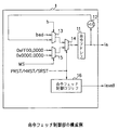
図6は、バス制御部4のリセットレジスタ4bを含む部分の詳細な構成例を示す図であり、当該リセットレジスタ4bに対するデータ書き込みの流れを示している。図6に示すように、リセットレジスタ4bは、PD,HD,SD,HS,SSという5ビット分のレジスタから構成されている。
FIG. 6 is a diagram showing a detailed configuration example of a portion including the
このうちPD,HD,SDの各ビットは、直前のリセット要因を示すためのレジスタであり、PDビットは電源投入時における初期起動リセット、HDビットはクロック供給再開時における再起動リセット、SDビットはデバッグ時等におけるプログラム再起動リセットであることを示す。これらの3ビットは、リセット要因の識別情報を保持する本発明の情報保持手段に相当する。 Of these, the PD, HD, and SD bits are registers for indicating the immediately preceding reset factor, the PD bit is the initial start reset when the power is turned on, the HD bit is the restart reset when the clock supply is resumed, and the SD bit is Indicates a program restart reset during debugging. These 3 bits correspond to the information holding means of the present invention that holds the identification information of the reset factor.
また、残りのHS,SSの2ビットは、図示しない外部バスマスタからここに書き込みを行うことにより、再起動リセット信号HRSTあるいはプログラムリセット信号SRSTに相当するリセット信号(HRST'、SRST')をバス制御部4の内部で発生するためのものであり、本発明のリセット内部発生手段を構成する。すなわち、このHSビットおよびSSビットの出力は、それぞれ再起動リセット信号HRSTおよびプログラムリセット信号SRSTと共にORゲート51,52に供給され、何れか有効な方が後段に供給される。
Further, the remaining 2 bits of HS and SS are written in here by an external bus master (not shown), thereby controlling the reset signal (HRST ′, SRST ′) corresponding to the restart reset signal HRST or the program reset signal SRST. This is generated inside the
上記リセットレジスタ4b内のPD,HD,SDの各ビットと、初期起動リセット信号PRST、再起動リセット信号HRSTおよびプログラムリセット信号SRSTとの間には、数個の論理ゲート51〜57が適当に配置されており、PD,HD,SDの3つのビットうち何れか1つのビットのみが"1"に設定されるようになっている。
すなわち、初期起動リセット信号PRSTがアサートされた場合にはPDビットが"1"にセットされる。また、外部からの再起動リセット信号HRSTがアサートされた場合、あるいはHSビットに書き込みが行われて内部での再起動リセット信号HRST'がアサートされた場合には、HDビットが"1"にセットされる。また、外部からのプログラムリセット信号SRSTがアサートされた場合、あるいはSSビットに書き込みが行われて内部でのプログラムリセット信号SRST'がアサートされた場合には、SDビットが"1"にセットされる。 That is, when the initial activation reset signal PRST is asserted, the PD bit is set to “1”. When the external restart reset signal HRST is asserted, or when the internal restart reset signal HRST ′ is asserted by writing to the HS bit, the HD bit is set to “1”. Is done. When the external program reset signal SRST is asserted or when the SS bit is written and the internal program reset signal SRST ′ is asserted, the SD bit is set to “1”. .
また、上記数個の論理ゲート51〜57を適当に配置することにより、3種類のリセット間に、
PRST>HRST>SRST
の優先順位を持たせている。そして、新たにリセット要因が発生するまでは、直前のリセット要因をPD,HD,SDの各ビットに保持し続けるようになっている。
Further, by appropriately arranging the above-mentioned
PRST>HRST> SRST
Is given priority. Until the reset factor is newly generated, the immediately previous reset factor is held in the PD, HD, and SD bits.
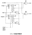
図7は、クロック制御部5の構成例を示す図である。クロック制御部5は、外部から供給された外部クロックCLOCKから2つの内部クロックbck,cckを発生し、これをプロセッサ10の内部へ供給している。すなわち、本実施形態では、図1に示したように、バス制御部4とその他の部分への内部クロックはbck,cckの別系統で供給されている。
FIG. 7 is a diagram illustrating a configuration example of the clock control unit 5. The clock control unit 5 generates two internal clocks bck and cck from the external clock CLOCK supplied from the outside, and supplies them to the inside of the
また、本実施形態では、命令実行部2からの指示により、プロセッサ10内部へのクロック供給を一時的に停止させることを可能としている。例えば、消費電力を低減させるために、プロセッサ10のアイドル状態が一定時間続くと、命令実行部2からクロック制御部5に対してクロック停止信号stopがアサートされる。
In the present embodiment, the clock supply to the
このとき、バス制御部4も含めたプロセッサ10全体に対する内部クロックbck,cckを共に停止させる第1のモードと、プロセッサ10内のバス制御部4を除く部分に対する第2の内部クロックcckのみを停止させる第2のモードとの何れかを選択することができる。選択されたモードに応じて、命令実行部2からクロック停止信号stopbcあるいはstopcがアサートされる。
At this time, only the first mode for stopping both the internal clocks bck and cck for the
プロセッサ10の全体を停止させるためのクロック停止信号stopbcは、2つのORゲート61,65に供給される。ORゲート61を通過したクロック停止信号stopbcは、Cレジスタ62に保持された後、ANDゲート64の負論理端子に供給され、ANDゲート64の正論理端子に供給される外部クロックCLOCKとの論理積がとられて内部クロックcckとして出力される。
A clock stop signal stopbc for stopping the
一方、ORゲート65を通過したクロック停止信号stopbcは、Bレジスタ66に保持された後、ANDゲート68の負論理端子に供給され、ANDゲート68の正論理端子に供給される外部クロックCLOCKとの論理積がとられて内部クロックbckとして出力される。
On the other hand, the clock stop signal stopbc that has passed through the
このような構成により、クロック停止信号stopbcがアサートされたときには、ANDゲート64,68の負論理端子には共に"1"の信号が入力されるので、2つの内部クロックbck,cckの供給が停止されることとなる。
With this configuration, when the clock stop signal stopbc is asserted, the signals “1” are input to the negative logic terminals of the AND
また、プロセッサ10内のバス制御部4以外を停止させるためのクロック停止信号stopcは、ORゲート61にのみ供給される。このORゲート61を通過したクロック停止信号stopcは、Cレジスタ62に保持された後、ANDゲート64の負論理端子に供給され、ANDゲート64の正論理端子に供給される外部クロックCLOCKとの論理積がとられて内部クロックcckとして出力される。
Further, the clock stop signal stopc for stopping other than the
このような構成により、クロック停止信号stopcがアサートされたときには、ANDゲート64の負論理端子には"1"の信号が入力されるので、内部クロックcckの供給が停止されることとなる。一方、クロック停止信号stopcはORゲート65には供給されないので、当該クロック停止信号stopcのアサートによってANDゲート68の負論理端子に"1"の信号が入力されることはなく、内部クロックbckの供給は継続して行われることとなる。
With such a configuration, when the clock stop signal stopc is asserted, the signal “1” is input to the negative logic terminal of the AND
なお、上記ORゲート61,65には、それぞれANDゲート63,67の出力も供給されている。ANDゲート63は、その正論理端子に供給されるCレジスタ62の出力と、負論理端子に供給される起動信号wupとの論理積をとってORゲート61に供給する。また、ANDゲート67は、その正論理端子に供給されるBレジスタ66の出力と、負論理端子に供給される起動信号wupとの論理積をとってORゲート65に供給する。
The OR
また、上記Cレジスタ62およびBレジスタ66の記憶内容は、初期起動リセット信号PRST、再起動リセット信号HRST、あるいは外部バスマスタ等からリセットレジスタ4b(図6のHSビット)への書き込みにより発生する内部再起動リセット信号HRST'をアサートすることによって書き換えられるようになっている。
The contents stored in the
例えば、バス制御部4に対してのみ内部クロックbckが供給されている状態では、内部再起動リセット信号HRST'のアサートにより、バス制御部4以外の部分に対する内部クロックcckの供給を再開できるように構成されている。また、プロセッサ10の全体に対して内部クロックbck,cckの供給が停止された状態では、初期起動リセット信号PRSTあるいは再起動リセット信号HRSTをアサートすることにより、当該内部クロックbck,cckの供給を再開できるように構成されている。
For example, in a state where the internal clock bck is supplied only to the
次に、以上のように構成した本実施形態によるプロセッサ10を単独で用いた場合の起動シーケンスについて、以下に説明する。
まず、装置の電源投入時における初期起動リセット信号PRSTによる起動処理シーケンスについて説明する。
Next, a startup sequence when the
First, a startup process sequence by the initial startup reset signal PRST when the apparatus is turned on will be described.
装置の電源投入時には、まず、初期起動リセット信号PRSTがアサートされてハードウェア的な初期化処理が行われる。このとき、バス制御部4内の領域指定レジスタ4aやリセットレジスタ4bを含むプロセッサ10内の各種レジスタの値が、例えば全て"0"に初期化される。
When the apparatus is powered on, first, the initial activation reset signal PRST is asserted to perform hardware initialization processing. At this time, the values of various registers in the
そして、このハードウェア的な初期化処理を行うのに必要十分な時間だけ初期起動リセット信号PRSTがアサートされ、電源が安定すると、上記初期起動リセット信号PRSTがネゲートされる。初期起動リセット信号PRSTがネゲートされると、続いてソフトウェア的な初期化処理を行うために、リセットベクタで指示されるアドレスに従って初期化プログラムの読み出しが行われる。 Then, the initial activation reset signal PRST is asserted for a time sufficient for performing the hardware initialization process, and when the power supply is stabilized, the initial activation reset signal PRST is negated. When the initial activation reset signal PRST is negated, the initialization program is read in accordance with the address indicated by the reset vector in order to perform software initialization processing.
電源投入直後では、RAM6に有効な初期化プログラムのデータが保持されていないため、アドレス選択信号MSの値は"1"に設定されている。これにより命令フェッチ制御部1は、初期アドレス"0xFF00_0000"からの命令フェッチ要求を発行する。
Immediately after the power is turned on, since the valid initialization program data is not held in the
これに応じてバス制御部4では、与えられた"0xFF00_0000"の要求アドレスaddが、領域指定レジスタ4a内の先頭アドレスASRおよび領域サイズAMRにより指定されるRAM6のアドレス領域に含まれているか否かを判定し、その結果に応じてRAM6あるいはROM9の何れかにアクセスする。この時点では、RAM6のアドレス領域はφに初期化されており、与えられた要求アドレスaddもROM9のアドレス領域を指定しているため、バス制御部4は外部バス7,8上に接続されたROM9に対してアクセスすることになる。
In response to this, the
ROM9に格納されている初期化プログラムは、その最初のシーケンスにおいてリセットレジスタ4bの値を参照するように規定されている。電源投入直後においては、リセットレジスタ4b内のPDビットが"1"にセットされていることを確認して、初期起動リセット信号PRSTがネゲートされた場合に必要な処理を含むルーチンを実行する。
The initialization program stored in the ROM 9 is defined so as to refer to the value of the
このようにしてプロセッサ10が起動した後、RAM6をアクセスするために必要なアドレス情報(先頭アドレスASRおよび領域サイズAMR)を領域指定レジスタ4aに設定する。図2の例においては、先頭アドレスASRに"0x0000_0000"、領域サイズAMRに"0x01FF_FFFF"の値を設定し、RAM6のアドレス領域として32Mバイトを実装する。そして、領域指定レジスタ4aに必要な値を設定した後は、アドレス選択信号MSの値を"0"に切り替えるとともに、外部バス7,8上に接続されたROM9あるいはその他のデバイスから再起動用のプログラムをRAM6にロードしておく。
After the
次に、内部クロックの供給再開時における再起動リセット信号HRSTによる起動処理シーケンスについて説明する。
ここでは一例として、プロセッサ10の起動後、必要とされる処理が一定時間行われなかったことを契機としてプロセッサ10全体に内部クロックbck,cckの供給を停止させ、その後必要性が生じた時点で外部からの再起動リセット信号HRSTにより再起動を行う場合の再起動シーケンスを説明する。
Next, a startup process sequence by the restart reset signal HRST when the supply of the internal clock is resumed will be described.
Here, as an example, after the
外部より再起動リセット信号HRSTがアサートされると、クロック制御部5内で内部クロックbck,cckの供給を停止させているレジスタ(図7のCレジスタ62およびBレジスタ66)がリセットされ、内部クロックbck,cckの供給が再開される。これと同時に、メモリアクセスに必要な情報(領域指定レジスタ4a内の先頭アドレスASR、領域サイズAMRなど)を除いてハードウェア的な初期化処理が行われる。
When the restart reset signal HRST is asserted from the outside, the registers (
なお、プロセッサ10に接続されるローカルメモリとしてSDRAMを用いた場合、プロセッサ10は、上述の先頭アドレスASRや領域サイズAMRの情報を格納する領域指定レジスタ4aの他に、メモリアクセスに必要な情報として、DRAMの品種毎に異なるDRAMのオペレーション間の最小サイクル数を設定するコントロールレジスタ、DRAMに対するアクセスのモードを設定するアクセスモード制御レジスタ、DRAMのモード設定時にDRAMに対して書き込む情報を設定するモードセットレジスタ、DRAMのタイプ、バス幅、直結/DIMM使用などの情報を設定するコンフィギュレーションレジスタ、DRAMのRASアドレスビット数、CASアドレスビット数、バンクアドレスビット数を設定するアドレスナンバレジスタ、DRAMコントローラの状態を表すステータスレジスタ、DRAMのオートリフレッシュまたはセルフリフレッシュを設定するリフレッシュコントロールレジスタ、オートリフレッシュ時のリフレッシュ間隔を設定するリフレッシュタイマレジスタなどを備える。これらのレジスタは何れも、初期起動リセット信号PRSTによっては初期化されるが、再起動リセット信号HRSTやプログラムリセット信号SRSTによっては初期化されない。
When an SDRAM is used as the local memory connected to the
上記ハードウェア的な初期化処理の後、再起動リセット信号HRSTがネゲートされると、アドレス選択信号MS(=0)により選択されるアドレス"0x0000_0000"からの命令フェッチが開始される。このとき、領域指定レジスタ4a内の先頭アドレスASRおよび領域サイズAMRの値は、再起動リセット信号HRSTのアサートによっては初期化されていないので、このときの命令フェッチ要求はRAM6へと発行される。これにより、低速なROM9へのアクセスを不要とし、プロセッサ10の再起動処理を高速に行うことができる。
When the restart reset signal HRST is negated after the hardware initialization process, instruction fetch from the address “0x0000_0000” selected by the address selection signal MS (= 0) is started. At this time, since the values of the start address ASR and the area size AMR in the
なお、ここでアドレス選択信号MSの値として"1"を設定することにより、ROM9に対して命令フェッチ要求を発行するように指示することも可能である。プロセッサ10の再起動時にROM9からの命令フェッチが実行される場合には、ROM9に格納されている初期化プログラムは、その最初のシーケンスにおいてリセットレジスタ4bの値を参照し、リセットレジスタ4b内のHDビットがセットされていることを確認することで、既に電源投入時に領域指定レジスタ4aに設定されている情報の再設定処理を省くことができ、その分だけプロセッサ10の再起動処理を高速化することができる。
Here, it is also possible to instruct the ROM 9 to issue an instruction fetch request by setting “1” as the value of the address selection signal MS. When instruction fetch from the ROM 9 is executed when the
なお、内部クロックcckの供給停止後に外部からの再起動リセット信号HRSTによりプロセッサ10の再起動を行う場合や、内部クロックbck,cckあるいは内部クロックcckの供給停止後に、内部発生した再起動リセット信号HRST'によりプロセッサ10の再起動を行う場合の再起動シーケンスについても、その動作は以上と同様である。
It should be noted that after the supply of the internal clock cck is stopped, the
次に、プログラムリセット信号SRSTによる起動処理シーケンスについて説明する。
外部よりプログラムリセット信号SRSTがアサートされると、命令実行部2において現在実行中のプログラムが強制的に中断され、命令フェッチ制御部1に対してハードウェア的な初期化処理が行われる。
Next, the activation process sequence by the program reset signal SRST will be described.
When the program reset signal SRST is asserted from the outside, the program currently being executed in the
その後、プログラムリセット信号SRSTがネゲートされると、アドレス選択信号MS(=0)により選択されるアドレス"0x0000_0000"からの命令フェッチが開始される。このとき、領域指定レジスタ4a内の先頭アドレスASRおよび領域サイズAMRの値は、プログラムリセット信号SRSTのアサートによっては初期化されていないので、このときの命令フェッチ要求はRAM6へと発行される。これにより、低速なROM9へのアクセスを不要とし、プロセッサ10の再起動処理を高速に行うことができる。
Thereafter, when the program reset signal SRST is negated, instruction fetch from the address “0x0000 — 0000” selected by the address selection signal MS (= 0) is started. At this time, since the values of the start address ASR and the area size AMR in the
なお、ここでアドレス選択信号MSの値として"1"を設定することにより、ROM9に対して命令フェッチ要求を発行するように指示することも可能である。プログラムリセット時にROM9からの命令フェッチが実行される場合には、ROM9に格納されている初期化プログラムは、その最初のシーケンスにおいてリセットレジスタ4bの値を参照し、リセットレジスタ4b内のSDビットがセットされていることを確認することで、命令フェッチ制御部1のレジスタに対してのみ必要な再設定処理を行い、その他の不要な処理を省くことができ、その分だけプロセッサ10の再起動処理を高速化することができる。
Here, it is also possible to instruct the ROM 9 to issue an instruction fetch request by setting “1” as the value of the address selection signal MS. When instruction fetch from the ROM 9 is executed at the time of program reset, the initialization program stored in the ROM 9 refers to the value of the
以上詳しく説明したように、本実施形態のプロセッサ10によれば、ソフトウェア的な初期化処理を行う際に、初期起動リセット信号PRST、再起動リセット信号HRST、プログラムリセット信号SRSTの各リセット信号とアドレス選択信号MSとを用いた指示に応じて、外部バス7,8に接続されたROM9からの起動か、プロセッサ10にローカルメモリとして接続されたRAM6からの起動かを選択することができる。
As described above in detail, according to the
これにより、電源投入後において内部クロックbck,cckの供給が停止された後の再起動時には、高速なRAM6から再起動用の初期化プログラムを読み出してプロセッサ10の起動を行うことができ、その再起動処理を高速に行うことができる。また、再起動時にROM9に対してアクセスする場合でも、リセットレジスタ4bの値を読むことで、ROM9に格納されている初期化プログラム内で分岐して、リセット内容に応じた起動処理のみを選択的に実行することができる。したがって、低消費電力化のためにプロセッサ10でクロック供給の停止と起動が頻繁に行われるようなシステムでも、システムの起動待ちという無駄な時間を格段に短くすることができる。
Thereby, at the time of restart after the supply of the internal clocks bck and cck is stopped after the power is turned on, the initialization program for restart can be read from the high-
また、上記のようなプロセッサ10を共有バスに複数接続してマルチプロセッサシステムを構成した場合においても、例えばスレーブプロセッサで内部クロックbck,cckの供給が一時的に停止された後の再起動時において、当該スレーブプロセッサは高速なRAM6から再起動用の初期化プログラムを読み出すことができ、その再起動処理を高速に行うことができる。その際、スレーブプロセッサからは外部バス7,8に対して命令フェッチ要求を発行することがないので、複数のプロセッサからROM9へのアクセスが競合することがなく、バス調停の処理も不要とすることができる。
Further, even when a multiprocessor system is configured by connecting a plurality of
さらに、上述のようにマルチプロセッサシステムを構成した場合でも、それぞれのプロセッサにおいて実行すべき初期化プログラムを格納したメモリの先頭アドレスがアドレス選択信号MSにより選択される。したがって、どのプロセッサがROM9内のどのプログラムを実行するのかを判別するための機構も不要となり、システムの構成を簡素化することができる。 Further, even when the multiprocessor system is configured as described above, the start address of the memory storing the initialization program to be executed by each processor is selected by the address selection signal MS. Therefore, a mechanism for determining which processor executes which program in the ROM 9 becomes unnecessary, and the system configuration can be simplified.
次に、本発明によるデータ処理システムの第2の実施形態について説明する。
図8は、第2の実施形態によるプロセッサをスレーブプロセッサとして搭載したマルチプロセッサシステムの構成例を示すブロック図である。
Next, a second embodiment of the data processing system according to the present invention will be described.
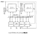
FIG. 8 is a block diagram illustrating a configuration example of a multiprocessor system in which the processor according to the second embodiment is mounted as a slave processor.
図8において、71はマスタープロセッサ、72はスレーブプロセッサであり、それぞれに対してローカルメモリであるRAM73,74が接続されている。共有バスである外部バス7,8には、これらのマスタープロセッサ71、スレーブプロセッサ72の他に、ROM9、共有メモリ75、メモリ−メモリ間のダイレクトデータ転送を行うDMAC(Direct Memory Access Controller )76、スレーブプロセッサ72を制御する信号を生成するASIC(Application Specific Intergrated Ciucuit)77が接続されている。
In FIG. 8, 71 is a master processor, 72 is a slave processor, and
上記マスタープロセッサ71は、電源投入後は常時動作しているものであり、通常のプロセッサを用いることが可能である。一方、スレーブプロセッサ72は、電源投入後において、低消費電力化のために内部クロックの供給停止および起動を行うことができるようになされたものであり、本実施形態に特有のプロセッサが用いられる。
The
図9は、本実施形態に係るスレーブプロセッサ72の構成例を示すブロック図である。
本実施形態のスレーブプロセッサ72は、図1に示したプロセッサ10とほぼ同様の構成を有するが、命令フェッチ制御部81およびバス制御部84の構成が図1と異なっている。また、命令フェッチ制御部81には、プログラムリセット信号SRSTやアドレス選択信号MSに加えて、起動抑止信号WAITが入力されている。
FIG. 9 is a block diagram illustrating a configuration example of the
The
上記命令フェッチ制御部81は、図10のように構成されている。図10に示すように、本実施形態の命令フェッチ制御部81では、図3に示した命令フェッチ制御部1と比べて、起動抑止信号WAITの論理を反転するインバータ85、このインバータ85の出力と命令フェッチ制御ロジック16の出力との論理積をとるANDゲート86とが追加されている。
The instruction fetch
このように構成することにより、命令フェッチ制御ロジック16がプロセッサ72の命令実行状況やキャッシュ制御部の状況等を判断して命令フェッチ要求iavalの発行が可能な状態となっても、さらに外部からの起動抑止信号WAITがネゲートされない限り、命令フェッチ要求iavalはキャッシュユニット3に対して発行されることはない。このように、インバータ85およびANDゲート86によって本発明の起動抑止手段が構成される。
With this configuration, even if the instruction fetch
また、上記バス制御部84は、図4に示したのとほぼ同様に構成されている。ただし、本実施形態において外部バス制御部23は、規定されたプロトコルに従って外部バス7,8上に発生したトランザクションが他のデバイスから自プロセッサに対する要求であった場合、そのコマンドを取り込んで該当する処理を開始する機構を有している。
The
具体的には、外部バス制御部23は、外部バス7,8上に発生したトランザクションを常に監視し、有効なトランザクションが生じた場合に、そのアドレス情報を取り込んで自プロセッサ内の資源に対してあらかじめ割り当てられたアドレス情報との比較を行う。この比較の結果、自プロセッサ内の資源に対する要求と認識された場合は、そのトランザクションのコマンドを取り込み、上記アドレス情報によって指定される内部資源へのアクセスを開始する。
Specifically, the external
図11は、この外部バス制御部23の構成例を示す図である。図11に示すように、本実施形態の外部バス制御部23は、キャッシュユニット3からのコマンドとライトデータとを保持する4段のキャッシュコマンドバッファ91、外部バス7,8からの応答データをキャッシュユニット3へ送り出すための応答データバッファ92、外部バス7,8からのコマンドとライトデータとを保持する4段のバスコマンドバッファ93、ローカルメモリであるRAM74からの読み出しデータを受ける読出データバッファ94を備えている。
FIG. 11 is a diagram illustrating a configuration example of the external
外部バス制御部23は更に、上記4段のキャッシュコマンドバッファ91に格納されたデータの何れかを選択するセレクタ95、上記4段のバスコマンドバッファ93に格納されたデータの何れかを選択するセレクタ96、アドレスバス7の調停を行うコマンド調停部97、データバス8の調停を行うデータ調停部98およびメモリマップされたレジスタ99を備えている。
The external
上記レジスタ99は、図9に示した領域指定レジスタ4aおよびリセットレジスタ4bに相当するものであり、RAM74の先頭アドレスASRおよび領域サイズAMRの情報、図6に示したリセット種識別情報PD,HD,SDおよび内部リセット書込情報HS,SSを保持している。このレジスタ99には、キャッシュユニット3からのコマンド、外部バス7,8からのコマンドの両方がアクセスできるように構成されている。
The
このように、上述した第1の実施形態では先頭アドレスASRおよび領域サイズAMRを格納する領域指定レジスタ4aはバスI/F21内に備えられていたが(図4参照)、第2の実施形態では、これらの情報を格納するレジスタ99は、外部バス制御部23内に備えられている。この場合、バスI/F21は、外部バス制御部23からこのレジスタ99に設定された値を受け取っている。
As described above, in the first embodiment described above, the
次に、以上のように本実施形態によるプロセッサ72をスレーブプロセッサとして用いたマルチプロセッサシステムの起動シーケンスについて、以下に説明する。
まず、装置の電源投入時における初期起動リセット信号PRSTによる起動処理シーケンスについて説明する。
Next, the startup sequence of the multiprocessor system using the
First, a startup process sequence by the initial startup reset signal PRST when the apparatus is turned on will be described.
装置の電源投入時には、マスタープロセッサ71に対しては初期起動リセット信号PRSTがアサートされ、スレーブプロセッサ72に対しては初期起動リセット信号PRSTと起動抑止信号WAITとがアサートされる。初期起動リセット信号PRSTがアサートされると、マスタープロセッサ71およびスレーブプロセッサ72の両方にてハードウェア的な初期化処理が行われる。このとき、先頭アドレスASRや領域サイズAMRの情報を含むプロセッサ71,72内のレジスタの値が、例えば全て"0"に初期化される。
When the apparatus is turned on, an initial activation reset signal PRST is asserted to the
そして、ハードウェア的な初期化処理が行われ、電源が安定すると、上記初期起動リセット信号PRSTがネゲートされる。マスタープロセッサ71では、初期起動リセット信号PRSTがネゲートされると、続いてソフトウェア的な初期化処理を行うために、リセットベクタで指示されるアドレスに従って、外部バス7,8に接続されたROM9から初期化プログラムの読み出しが行われる。このとき、起動抑止信号WAITはアサートされたままである。そのため、スレーブプロセッサ72では、命令フェッチ要求iavalは発行されず、初期化プログラムの読み出しは行われない。
When the hardware initialization process is performed and the power supply is stabilized, the initial activation reset signal PRST is negated. In the
マスタープロセッサ71における初期化処理が完了すると、マスタープロセッサ71は、スレーブプロセッサ72の内部資源(先頭アドレスASR、領域サイズAMRの情報など)を外部バス7,8を介して適切な値に設定する。つまり、マスタープロセッサ71から図11のデータ調停部98を介してレジスタ99に書き込みを行うことにより、スレーブプロセッサ72に接続されたRAM74のアドレス領域を適切に設定する。そして、マスタープロセッサ71は、DMAC76を起動して、スレーブプロセッサ72が必要とする初期化プログラムを、例えばROM9からRAM74に転送する。
When the initialization process in the
このとき、スレーブプロセッサ72が備える図11の外部バス制御部23においては、メモリ−メモリ間のデータダイレクト転送のためにDMAC76よりアドレスバス7を介して与えられたアドレスが、レジスタ99に設定された先頭アドレスASRおよび領域サイズAMRの対で指定されるRAM74のアドレス領域内のものかどうかを判定する。
At this time, in the external
この場合、レジスタ99内の先頭アドレスASRおよび領域サイズAMRの各情報には、事前にRAM74のアドレス領域がセットされているので、外部バス制御部23は、ROM9からデータバス8を介して送られてきた初期化プログラムのデータをメモリ制御部22に送り、RAM74の該当するアドレス領域に対して初期化プログラムを格納することになる。
In this case, since the address area of the
本実施形態では、先頭アドレスASRおよび領域サイズAMRの情報がバスI/F21ではなく外部バス制御部23内に保持されているので、バスI/F21を用いることなく、メモリ制御部22と外部バス制御部23だけで初期化プログラムの転送を行うことができる。また、DMAC76はマスタープロセッサ71と独立して転送処理を実行するため、マスタープロセッサ71の処理部を煩わせることなく、スレーブプロセッサ72のRAM74に必要なソフトウェアの転送処理を行うことができる。
In this embodiment, since the information of the head address ASR and the area size AMR is held in the external
DMAC76は、転送処理の完了を割り込み信号を用いてマスタープロセッサ71に通知する。DMAC76からの転送完了割り込み信号を検出したマスタープロセッサ71は、その後必要が生じた時点でASIC77にアクセスし、起動抑止信号WAITをネゲートさせる。この起動抑止信号WAITがネゲートされることにより、スレーブプロセッサ72では、命令フェッチ制御部81が、"0"の値が設定されたアドレス選択信号MSによって選択される初期アドレス"0x0000_0000"からの命令フェッチ要求iavalをキャッシュユニット3を介してバス制御部84に発行する。
The
このとき、バス制御部84内のバスコマンド制御部24では、当該命令フェッチ要求iavalと共に与えられる要求アドレスaddと、外部バス制御部23内のレジスタ99から受け取った先頭アドレスASRおよび領域サイズAMRの値とを比較し、要求アドレスaddがRAM74のアドレス領域内のものかどうかを判定する。
At this time, in the bus
ここでは、先頭アドレスASRおよび領域サイズAMRにはRAM74のアドレス領域がセットされているので、バスコマンド制御部24は、命令フェッチ要求iavalがRAM74に対する要求であると判断し、メモリ制御部22に対して命令フェッチ要求を発行する。この命令フェッチ要求を受けたメモリ制御部22は、メモリI/F28を介して接続されたRAM74をアクセスして上記要求アドレスaddに対応する命令データを読み出し、それを命令実行部2に供給して実行する。
Here, since the address area of the
その後、必要とされる処理がスレーブプロセッサ72において一定時間行われなかったとすると、そのことを契機として、スレーブプロセッサ72の命令実行部2がクロック制御部5に対してクロック停止信号stopcを供給することにより、バス制御部84以外に供給されている内部クロックcckの供給を停止させる。
Thereafter, if the required processing has not been performed in the
マスタープロセッサ71は、その後必要性が生じた時点で、スレーブプロセッサ72が備えるレジスタ99のHSビットに書き込みを行うことにより、内部クロックcckの供給を再開させるとともに、ハードウェア的な初期化処理およびソフトウェア的な初期化処理を実行する。このとき、ソフトウェア的な初期化処理を行うために必要な初期化プログラムの起動シーケンスは、第1の実施形態で述べたのと同様であり、RAM74からの高速な再起動が実行される。
The
このように、第2の実施形態では、電源投入時における初期起動リセット信号PRSTによる起動処理シーケンスにおいて、スレーブプロセッサ72では、起動抑止信号WAITのアサートにより命令フェッチ要求iavalの発行を停止している間にRAM74に初期化プログラムを転送しておき、その後起動抑止信号WAITをネゲートしてRAM74に対して命令フェッチ要求iavalを発行するようにしている。
As described above, in the second embodiment, in the activation processing sequence based on the initial activation reset signal PRST when the power is turned on, the
したがって、電源投入時における起動処理シーケンスにおいても、スレーブプロセッサ72は共有バスを介してROM9にアクセスしなくても済む。これにより、高速なRAM74から初期化プログラムを読み出してスレーブプロセッサ72の起動を行うことができる。また、共有バス上に接続された複数のプロセッサがROM9に対するアクセスを一斉に開始することがなく、共有バスのアービトレーションを不要とすることもでき、起動処理を高速に行うことができる。
Therefore, the
また、スレーブプロセッサ72において実行すべき初期化プログラムはRAM74に格納され、スレーブプロセッサ72の初期化処理を行う際には、アドレス選択信号MSにより選択したこのRAM74の先頭アドレスから初期化プログラムを読み出せば良いので、どのプロセッサがどのプログラムを実行するのかを判別するための機構も不要となり、システムの構成を簡素化することができる。
The initialization program to be executed in the
なお、以上に説明した各実施形態は、何れも本発明を実施するにあたっての具体化の一例を示したものに過ぎず、これらによって本発明の技術的範囲が限定的に解釈されてはならないものである。すなわち、本発明はその精神、またはその主要な特徴から逸脱することなく、様々な形で実施することができる。 Note that each of the embodiments described above is merely an example of a specific example for carrying out the present invention, and the technical scope of the present invention should not be construed as being limited thereto. It is. In other words, the present invention can be implemented in various forms without departing from the spirit or main features thereof.
例えば、以上の各実施形態では、外部から与えられるアドレス選択信号MSに基づいて初期化プログラムの開始アドレスを選択していたが、開始アドレスの選択が内部で行われるようにしても良い。図12は、その場合の命令フェッチ制御部の構成例を示す図である。この例では、LSI内部のレジスタに設定した値に従って、再起動アドレスの選択を行うようにしている。なお、図12において、図10に示したブロックと同じブロックには同一の符号を付している。 For example, in each of the above embodiments, the start address of the initialization program is selected based on the address selection signal MS given from the outside, but the start address may be selected internally. FIG. 12 is a diagram illustrating a configuration example of the instruction fetch control unit in that case. In this example, the restart address is selected according to the value set in the register in the LSI. In FIG. 12, the same blocks as those shown in FIG. 10 are denoted by the same reference numerals.
図12に示す命令フェッチ制御部101では、図10に示した命令フェッチ制御部81に対して、数個の論理ゲート102〜105とレジスタ106とが追加されている。ANDゲート102は、アドレス選択信号MSと初期起動リセット信号PRSTとの論理積をとってその結果をORゲート105に出力する。ANDゲート103は、信号btdir と、信号 set_btdir と、初期起動リセット信号PRSTの論理反転信号との論理積をとってその結果をORゲート105に出力する。また、ANDゲート104は、信号 set_btdir の論理反転信号と、初期起動リセット信号PRSTの論理反転信号と、レジスタ106の出力信号との論理積をとってその結果をORゲート105に出力する。
In the instruction fetch
上記ORゲート105は、各ANDゲート102〜104の出力結果の論理和をとってその結果をレジスタ106に出力する。これによりレジスタ106は、初期起動リセット信号PRSTのアサート時には、外部端子からアドレス選択信号MSの値を取り込む。また、初期起動リセット信号PRSTがネゲートされ、信号 set_btdir がアサートされている時は、信号btdir の値を取り込む。また、これ以外の状態の時は、記憶されている値を保持する。ここで、信号btdir ,set_btdir は、命令実行部2がレジスタ106への書き込み命令を実行することによりアサートされるものとする。
The OR
セレクタ15は、レジスタ106に保持されている値に応じて、"0x0000_0000"または"0xFF00_0000"の何れかのアドレスを選択する。例えば、レジスタ106に保持されている値が"1"のときはアドレス"0xFF00_0000"を選択し、レジスタ106に保持されている値が"0"のときはアドレス"0x0000_0000"を選択する。
The
以上のように構成することにより、電源投入時には初期起動リセット信号PRSTがアサートされ、外部端子からアドレス選択信号MSの値を取り込んで初期化プログラムの開始アドレスを選択する。また、クロック供給停止前に命令実行部2がレジスタ106への書き込み命令を実行することで当該レジスタ106の値を"0"に設定しておくことで、クロック供給の停止後における再起動リセット信号HRSTによる再起動時には、レジスタ106内の"0"の値を参照して、初期化プログラムの開始アドレスとして"0x0000_0000"(RAMの先頭アドレス)を選択することができる。
With the configuration described above, the initial activation reset signal PRST is asserted when the power is turned on, and the value of the address selection signal MS is taken from the external terminal to select the start address of the initialization program. Further, the
なお、ここではアドレス選択信号MSの外部端子とレジスタ設定との混合型を示しているが、レジスタ設定のみの構成とすることも可能である。また、レジスタ106を他のユニットに移動してメモリマップとすることで、スレーブプロセッサの動作時にマスタープロセッサからレジスタ106への書き込みを可能とすることができ、初期化プログラムの開始アドレスの選択をマスタープロセッサから制御可能とする構成も可能である。
Note that, here, a mixed type of the external terminal of the address selection signal MS and the register setting is shown, but it is also possible to adopt a configuration with only register setting. Also, by moving the
上述したように、アドレス選択信号に基づいて、ローカルメモリまたはバスを介して接続される外部メモリに格納された初期化プログラムの開始アドレスを選択するアドレス選択手段を設けたので、電源投入後において内部クロックの供給が停止された後の再起動時には、高速なローカルメモリから再起動用の初期化プログラムを読み出してプロセッサの起動を行うことができ、その再起動処理を高速に行うことができる。これにより、システムの消費電力を抑制するとともにクロック停止状態からの高速な復帰を実現することができるようになる。 As described above, the address selection means for selecting the start address of the initialization program stored in the local memory or the external memory connected via the bus based on the address selection signal is provided. When restarting after the clock supply is stopped, the initialization program for restarting can be read from the high-speed local memory to start the processor, and the restarting process can be performed at high speed. As a result, the power consumption of the system can be suppressed and high-speed recovery from the clock stop state can be realized.
また、起動抑止信号に基づいて、初期化プログラムが格納されたメモリへのアクセス要求を抑止するアクセス抑止手段を備え、メモリへのアクセス要求を抑止している間に、外部バスを介して接続される外部メモリに格納された初期化プログラムをローカルメモリに転送しておき、アクセス要求の抑止の解除後には、ローカルメモリに格納された初期化プログラムの開始アドレスを選択するようにしたので、電源投入時における起動処理シーケンスにおいても外部メモリにアクセスすることなく、高速なローカルメモリから初期化プログラムを読み出して起動を行うことができる。また、外部バス上に接続された複数のプロセッサが外部メモリに対するアクセスを一斉に開始することがなくなり、共有バスのアービトレーションを不要とすることもできるので、起動処理を高速に行うことができる。
また、マルチプロセッサシステムを構成した場合に、どのプロセッサがどのプログラムを実行するのかを判別するための機構も不要となり、システムの構成を簡素化することができる。
In addition, an access suppression means for suppressing an access request to the memory storing the initialization program based on the activation suppression signal is provided, and is connected via an external bus while the access request to the memory is being suppressed. The initialization program stored in the external memory is transferred to the local memory, and after the access request suppression is canceled, the start address of the initialization program stored in the local memory is selected. Even in the activation process sequence at the time, the initialization program can be read from the high-speed local memory and activated without accessing the external memory. Also, a plurality of processors connected on the external bus do not start accessing the external memory all at once, and the arbitration of the shared bus can be made unnecessary, so that the startup process can be performed at high speed.
Further, when a multiprocessor system is configured, a mechanism for determining which processor executes which program is not required, and the system configuration can be simplified.
本発明の様々な形態をまとめると、以下のようになる。
(1)リセット信号に応じて、ハードウェア的な初期化処理を行った後でメモリから必要な初期化プログラムを読み込んでソフトウェア的な初期化処理を行うデータ処理システムであって、
アドレス選択信号に基づいて、ローカルメモリまたはバスを介して接続される外部メモリに格納された上記初期化プログラムの開始アドレスを選択するアドレス選択手段を備えたことを特徴とするデータ処理システム。
The various aspects of the present invention are summarized as follows.
(1) A data processing system for performing a software initialization process by reading a necessary initialization program from a memory after performing a hardware initialization process in response to a reset signal,
A data processing system comprising address selection means for selecting a start address of the initialization program stored in a local memory or an external memory connected via a bus based on an address selection signal.
(2)上記アドレス選択手段は、電源投入時に第1のリセット信号が外部より与えられるときは、上記アドレス選択信号に基づいて、上記外部メモリに格納された上記初期化プログラムの開始アドレスを選択することを特徴とする上記(1)に記載のデータ処理システム。 (2) The address selection means selects the start address of the initialization program stored in the external memory based on the address selection signal when the first reset signal is given from the outside at power-on. The data processing system according to (1) above, wherein
(3)上記アドレス選択手段は、クロック供給の停止後における再起動時に第2のリセット信号が外部より与えられるときは、上記アドレス選択信号に基づいて、上記ローカルメモリに格納された上記初期化プログラムの開始アドレスを選択することを特徴とする上記(1)に記載のデータ処理システム。 (3) When the second reset signal is given from the outside at the time of restart after the clock supply is stopped, the address selection means stores the initialization program stored in the local memory based on the address selection signal. The data processing system according to (1) above, wherein a start address is selected.
(4)上記第2のリセット信号が外部より与えられるときは、上記ハードウェア的な初期化処理では、上記ローカルメモリのアドレス領域を含むメモリアクセスに必要な情報以外を初期化することを特徴とする上記(3)に記載のデータ処理システム。 (4) When the second reset signal is given from the outside, the hardware initialization process initializes information other than information necessary for memory access including the address area of the local memory. The data processing system according to (3) above.
(5)上記アドレス選択手段は、強制的な初期化のために第3のリセット信号が外部より与えられるときは、上記アドレス選択信号に基づいて、上記ローカルメモリに格納された上記初期化プログラムの開始アドレスを選択することを特徴とする上記(1)に記載のデータ処理システム。 (5) When the third reset signal is given from the outside for compulsory initialization, the address selection means is configured to store the initialization program stored in the local memory based on the address selection signal. The data processing system according to (1), wherein a start address is selected.
(6)上記第3のリセット信号が外部より与えられるときは、上記ハードウェア的な初期化処理では、プログラムの命令フェッチを制御するフェッチ制御部を含む最小限の情報だけを初期化することを特徴とする上記(5)に記載のデータ処理システム。 (6) When the third reset signal is given from the outside, the hardware initialization process initializes only the minimum information including the fetch control unit that controls the instruction fetch of the program. The data processing system according to (5), characterized in that it is characterized in that
(7)上記ローカルメモリ内の初期化プログラムは、電源投入時に第1のリセット信号が外部より与えられたときに、上記外部メモリに格納された上記初期化プログラムを転送して格納することを特徴とする上記(1)に記載のデータ処理システム。 (7) The initialization program in the local memory transfers and stores the initialization program stored in the external memory when a first reset signal is given from the outside at power-on. The data processing system according to (1) above.
(8)上記第2のリセット信号と等価なリセット信号を装置内部で発生させるリセット内部発生手段を備えることを特徴とする上記(3)に記載のデータ処理システム。 (8) The data processing system according to (3), further comprising reset internal generation means for generating a reset signal equivalent to the second reset signal inside the apparatus.
(9)上記第3のリセット信号と等価なリセット信号を装置内部で発生させるリセット内部発生手段を備えることを特徴とする上記(5)に記載のデータ処理システム。 (9) The data processing system according to (5), further comprising a reset internal generation unit that generates a reset signal equivalent to the third reset signal inside the apparatus.
(10)データ処理システムに対して行われたリセット動作が第1のリセット、第2のリセットおよび第3のリセットの何れであるかを識別するための情報を保持する情報保持手段を備え、
上記初期化プログラムの命令に基づいて上記情報保持手段内の識別情報を読み取り、その結果に応じた処理を行うことを特徴とする上記(1)に記載のデータ処理システム。
(10) An information holding unit that holds information for identifying whether the reset operation performed on the data processing system is the first reset, the second reset, or the third reset,
The data processing system according to (1), wherein the identification information in the information holding unit is read based on an instruction of the initialization program, and processing according to the result is performed.
(11)リセット信号に応じて、ハードウェア的な初期化処理を行った後でメモリから必要な初期化プログラムを読み込んでソフトウェア的な初期化処理を行うデータ処理システムであって、
起動抑止信号に基づいて、上記初期化プログラムが格納されたメモリへのアクセス要求を抑止するアクセス抑止手段を備えたことを特徴とするデータ処理システム。
(11) A data processing system for performing a software initialization process by reading a necessary initialization program from a memory after performing a hardware initialization process in response to a reset signal,
A data processing system comprising: an access deterring unit that deters an access request to the memory storing the initialization program based on a start deterrence signal.
(12)アドレス選択信号に基づいて、ローカルメモリまたはバスを介して接続される外部メモリに格納された上記初期化プログラムの開始アドレスを選択するアドレス選択手段と、
上記アクセス抑止手段によって上記メモリへのアクセス要求を抑止している間に、上記外部メモリに格納された上記初期化プログラムを上記ローカルメモリに転送するデータ転送手段とを備え、
上記アクセス要求の抑止の解除後に上記アドレス選択手段は、上記アドレス選択信号に基づいて、上記ローカルメモリに格納された上記初期化プログラムの開始アドレスを選択することを特徴とする上記(11)に記載のデータ処理システム。
(12) Address selection means for selecting a start address of the initialization program stored in the local memory or an external memory connected via a bus based on an address selection signal;
Data transfer means for transferring the initialization program stored in the external memory to the local memory while the access suppression means is suppressing access requests to the memory,
(11) In the above (11), the address selection means selects the start address of the initialization program stored in the local memory based on the address selection signal after canceling the inhibition of the access request. Data processing system.
(13)上記ローカルメモリのアドレス領域を表す情報を保持するレジスタおよび、外部より与えられるリセット信号と等価なリセット信号を装置内部で発生させるための情報を保持するレジスタを備え、上記外部バスに接続された他のバスマスタデバイスからこれらのレジスタに対してアクセス可能であることを特徴とする上記(12)に記載のデータ処理システム。 (13) A register that holds information representing the address area of the local memory and a register that holds information for generating a reset signal equivalent to a reset signal supplied from the outside inside the apparatus, and is connected to the external bus The data processing system as described in (12) above, wherein these registers are accessible from another bus master device.
(14)共有バス上に複数のデータ処理装置が接続され、それぞれのデータ処理装置において、リセット信号に応じて、ハードウェア的な初期化処理を行った後でメモリから必要な初期化プログラムを読み込んでソフトウェア的な初期化処理を行うデータ処理システムであって、当該データ処理システムに含まれる少なくとも1つのデータ処理装置に、
アドレス選択信号に基づいて、ローカルメモリまたはバスを介して接続される外部メモリに格納された上記初期化プログラムの開始アドレスを選択するアドレス選択手段と、
起動抑止信号に基づいて、上記初期化プログラムが格納されたメモリへのアクセス要求を抑止するアクセス抑止手段と、
上記アクセス抑止手段によって上記メモリへのアクセス要求を抑止している間に、上記外部メモリに格納された上記初期化プログラムを上記ローカルメモリに転送するデータ転送手段とを備え、
上記アクセス要求の抑止の解除後に上記アドレス選択手段は、上記アドレス選択信号に基づいて、上記ローカルメモリに格納された上記初期化プログラムの開始アドレスを選択することを特徴とするデータ処理システム。
(14) A plurality of data processing devices are connected on the shared bus. In each data processing device, a hardware initialization process is performed according to a reset signal, and then a necessary initialization program is read from the memory. A data processing system that performs software initialization processing in at least one data processing device included in the data processing system,
An address selection means for selecting a start address of the initialization program stored in a local memory or an external memory connected via a bus based on an address selection signal;
An access deterring means for deterring an access request to the memory storing the initialization program based on an activation deterrent signal;
Data transfer means for transferring the initialization program stored in the external memory to the local memory while the access suppression means is suppressing access requests to the memory,
A data processing system wherein the address selection means selects a start address of the initialization program stored in the local memory based on the address selection signal after canceling the inhibition of the access request.
(15)上記データ転送手段によるデータ転送は、メモリ−メモリ間のダイレクト転送を行うDMACを用いて行うことを特徴とする上記(14)に記載のデータ処理システム。 (15) The data processing system according to (14), wherein the data transfer by the data transfer means is performed using a DMAC that performs direct memory-to-memory transfer.
1 命令フェッチ制御部
2 命令実行部
3 キャッシュユニット
4 バス制御部
4a 領域指定レジスタ
4b リセットレジスタ
5 クロック制御部
6 RAM(ローカルメモリ)
7 アドレスバス
8 データバス
9 ROM(外部メモリ)
10 プロセッサ
14,15 セレクタ(アドレス選択手段)
23 外部バス制御部
24 バスコマンド制御部
71 マスタープロセッサ
72 スレーブプロセッサ
73,74 RAM(ローカルメモリ)
76 DMAC
77 ASIC
81 命令フェッチ制御部
84 バス制御部
85 インバータ
86 ANDゲート
99 レジスタ
101 命令フェッチ制御部
106 レジスタ
PRST 初期起動リセット信号(第1のリセット信号)
HRST 再起動リセット信号(第2のリセット信号)
SRST プログラムリセット信号(第3のリセット信号)
MS アドレス選択信号
ASR 先頭アドレス情報
AMR 領域サイズ情報
PD,HD,SD リセット種識別ビット
HS,SS 内部リセット書込みビット
bck,cck 内部クロック
stopc,stopbc クロック停止信号
WAIT 起動抑止信号
DESCRIPTION OF SYMBOLS 1 Instruction fetch
7
10
23 External
76 DMAC
77 ASIC
81 Instruction fetch
HRST Restart reset signal (second reset signal)
SRST Program reset signal (third reset signal)
MS address selection signal ASR start address information AMR region size information PD, HD, SD reset type identification bit HS, SS internal reset write bit bck, cck internal clock stopc, stopbc clock stop signal WAIT start inhibition signal
Claims (3)
前記マスタープロセッサが、前記リセット信号の種類に基づいて、初期化プログラムがローカルメモリ又は外部メモリの何れにあるかを設定し、
前記スレーブプロセッサは、前記選択されたローカルメモリ又は外部メモリから初期化プログラムを読み出すことを特徴とする初期化方法。 In a system in which communication is performed between a master processor and a slave processor, a second initialization process in software is performed using an initialization program after performing a first initialization process in response to a reset signal. An initialization method,
The master processor sets whether the initialization program is in a local memory or an external memory based on the type of the reset signal,
The initialization method, wherein the slave processor reads an initialization program from the selected local memory or external memory.
The initialization method according to claim 1, wherein the reset signal is any one of an initial startup reset signal, a restart reset signal, and a program reset signal.
Priority Applications (1)
| Application Number | Priority Date | Filing Date | Title |
|---|---|---|---|
| JP2005139979A JP2005293609A (en) | 2005-05-12 | 2005-05-12 | Initialization method |
Applications Claiming Priority (1)
| Application Number | Priority Date | Filing Date | Title |
|---|---|---|---|
| JP2005139979A JP2005293609A (en) | 2005-05-12 | 2005-05-12 | Initialization method |
Related Parent Applications (1)
| Application Number | Title | Priority Date | Filing Date |
|---|---|---|---|
| JP2000006823A Division JP4144990B2 (en) | 2000-01-14 | 2000-01-14 | Data processing system and initialization method |
Publications (1)
| Publication Number | Publication Date |
|---|---|
| JP2005293609A true JP2005293609A (en) | 2005-10-20 |
Family
ID=35326394
Family Applications (1)
| Application Number | Title | Priority Date | Filing Date |
|---|---|---|---|
| JP2005139979A Pending JP2005293609A (en) | 2005-05-12 | 2005-05-12 | Initialization method |
Country Status (1)
| Country | Link |
|---|---|
| JP (1) | JP2005293609A (en) |
Cited By (1)
| Publication number | Priority date | Publication date | Assignee | Title |
|---|---|---|---|---|
| CN104683624A (en) * | 2013-11-27 | 2015-06-03 | 京瓷办公信息系统株式会社 | Electronic device and method for starting the electronic device |
-
2005
- 2005-05-12 JP JP2005139979A patent/JP2005293609A/en active Pending
Cited By (2)
| Publication number | Priority date | Publication date | Assignee | Title |
|---|---|---|---|---|
| CN104683624A (en) * | 2013-11-27 | 2015-06-03 | 京瓷办公信息系统株式会社 | Electronic device and method for starting the electronic device |
| JP2015103121A (en) * | 2013-11-27 | 2015-06-04 | 京セラドキュメントソリューションズ株式会社 | Electronics |
Similar Documents
| Publication | Publication Date | Title |
|---|---|---|
| US6978350B2 (en) | Methods and apparatus for improving throughput of cache-based embedded processors | |
| US20230214326A1 (en) | Computer Memory Expansion Device and Method of Operation | |
| JP4730742B2 (en) | Apparatus and method for atomic memory update of shared memory direct memory access | |
| JP3733842B2 (en) | Vector scatter instruction control circuit and vector type information processing apparatus | |
| US20080059663A1 (en) | Methods and Appartus for Providing Data Transfer Control | |
| JPH0272453A (en) | Multiprocessor computer system having shared memory and private cash memory | |
| JP4144990B2 (en) | Data processing system and initialization method | |
| US20110004731A1 (en) | Cache memory device, cache memory system and processor system | |
| JPH10207771A (en) | Method for shortening memory operation | |
| JPH11501750A (en) | Method and apparatus for performing speculative system memory reads | |
| JP4160228B2 (en) | Microprocessor | |
| CN114416637A (en) | A kind of SOC chip reset processing method, device, SOC chip and medium | |
| US5699553A (en) | Memory accessing device for a pipeline information processing system | |
| JP2005293609A (en) | Initialization method | |
| US9946665B2 (en) | Fetch less instruction processing (FLIP) computer architecture for central processing units (CPU) | |
| JP2005310176A (en) | Initialization method | |
| JPH0736704A (en) | Program down-loading system | |
| JP2002342162A (en) | Method for controlling memory access and host bridge | |
| JPH11184752A (en) | Data processing device and data processing system | |
| JPH06187230A (en) | Memory supervision control method | |
| WO2006024985A2 (en) | Method and apparatus for modifying an information unit using an atomic operation in a system with a mixed architecture | |
| JP2001043204A (en) | Cache memory controller | |
| JP2002108702A (en) | Microcomputer and data processing device | |
| KR19990026157A (en) | Method and device for controlling cache memory in multiprocessor system | |
| JPH06124235A (en) | Cache control system |
Legal Events
| Date | Code | Title | Description |
|---|---|---|---|
| A131 | Notification of reasons for refusal |
Free format text: JAPANESE INTERMEDIATE CODE: A131 Effective date: 20060613 |
|
| A521 | Written amendment |
Free format text: JAPANESE INTERMEDIATE CODE: A523 Effective date: 20060811 |
|
| A131 | Notification of reasons for refusal |
Free format text: JAPANESE INTERMEDIATE CODE: A131 Effective date: 20070116 |
|
| A02 | Decision of refusal |
Free format text: JAPANESE INTERMEDIATE CODE: A02 Effective date: 20070529 |