JP2005293574A - Data processing system and computer program which support system memory address with hole - Google Patents
Data processing system and computer program which support system memory address with hole Download PDFInfo
- Publication number
- JP2005293574A JP2005293574A JP2005076077A JP2005076077A JP2005293574A JP 2005293574 A JP2005293574 A JP 2005293574A JP 2005076077 A JP2005076077 A JP 2005076077A JP 2005076077 A JP2005076077 A JP 2005076077A JP 2005293574 A JP2005293574 A JP 2005293574A
- Authority
- JP
- Japan
- Prior art keywords
- logical
- memory
- physical
- physical address
- address range
- Prior art date
- Legal status (The legal status is an assumption and is not a legal conclusion. Google has not performed a legal analysis and makes no representation as to the accuracy of the status listed.)
- Granted
Links
Images


Classifications
-
- G—PHYSICS
- G06—COMPUTING OR CALCULATING; COUNTING
- G06F—ELECTRIC DIGITAL DATA PROCESSING
- G06F12/00—Accessing, addressing or allocating within memory systems or architectures
-
- G—PHYSICS
- G06—COMPUTING OR CALCULATING; COUNTING
- G06F—ELECTRIC DIGITAL DATA PROCESSING
- G06F12/00—Accessing, addressing or allocating within memory systems or architectures
- G06F12/02—Addressing or allocation; Relocation
- G06F12/0223—User address space allocation, e.g. contiguous or non contiguous base addressing
- G06F12/0292—User address space allocation, e.g. contiguous or non contiguous base addressing using tables or multilevel address translation means
-
- G—PHYSICS
- G06—COMPUTING OR CALCULATING; COUNTING
- G06F—ELECTRIC DIGITAL DATA PROCESSING
- G06F12/00—Accessing, addressing or allocating within memory systems or architectures
- G06F12/02—Addressing or allocation; Relocation
- G06F12/08—Addressing or allocation; Relocation in hierarchically structured memory systems, e.g. virtual memory systems
- G06F12/10—Address translation
Landscapes
- Engineering & Computer Science (AREA)
- Theoretical Computer Science (AREA)
- Physics & Mathematics (AREA)
- General Engineering & Computer Science (AREA)
- General Physics & Mathematics (AREA)
- Memory System Of A Hierarchy Structure (AREA)
- Memory System (AREA)
- Executing Machine-Instructions (AREA)
Abstract
Description
本発明は、一般に、改善されたデータ処理システム、特に、改善されたオペレーティング・システム作動のための方法及びデータ処理システムに関する。より詳細には、本発明は、メモリマップされた入力/出力物理アドレスを仮想化して、連続するシステムメモリアドレス・スペースを与えるための方法及びデータ処理システムを提供するものである。 The present invention relates generally to an improved data processing system, and more particularly to a method and data processing system for improved operating system operation. More particularly, the present invention provides a method and data processing system for virtualizing memory mapped input / output physical addresses to provide a contiguous system memory address space.
多くのデータ処理システムにおいては、入力/出力キャッシュ禁止アドレスは、システム・アドレス・スペースのアドレス範囲にマップされる。多くの場合、入力/出力キャッシュ禁止アドレスは、オペレーティング・システムによる使用のために割り振られたシステムメモリの多数の物理アドレス範囲の中間に、物理アドレスを有する。このような場合には、入力/出力キャッシュ禁止アドレスは、オペレーティング・システムがアドレス可能な別々のメモリのブロックの間に存在する、物理アドレスのメモリ「ホール」(hole)を呈するものとなる。 In many data processing systems, input / output cache inhibit addresses are mapped to address ranges in the system address space. In many cases, the input / output cache inhibit address has a physical address in the middle of multiple physical address ranges of system memory allocated for use by the operating system. In such a case, the input / output cache inhibit address represents a physical address memory “hole” that exists between separate blocks of memory addressable by the operating system.
オペレーティング・システムは、ホールをもつシステムメモリアドレスをサポートできないことがある。例えば、2つのメモリアレイをもつ幾つかの構成においては、Linux(Linus Torvaldsの商標)のオペレーティング・システムは、ホールをもつメモリアドレスを処理できないことがある。このような状況においては、オペレーティング・システムのカーネルを、メモリホールに対応するように変更することができる。しかしながら、このような解決策は時間がかかり、幾つかのサーバプログラムの機能性、可用性、及び、このような欠陥をもつオペレーティング・システムのバージョンを十分にサポートするデータ処理システムの能力を脅かすことになる。 The operating system may not be able to support system memory addresses with holes. For example, in some configurations with two memory arrays, the Linux (Linus Torvalds trademark) operating system may not be able to handle memory addresses with holes. In such situations, the operating system kernel can be modified to accommodate memory holes. However, such a solution is time consuming and threatens the functionality, availability of some server programs, and the ability of the data processing system to fully support such flawed operating system versions. Become.
従って、ホールをもつシステムメモリアドレスをサポートするデータ処理システムを提供することが有益である。さらに、オペレーティング・システムのカーネルを変更することなく、ホールをもつシステムメモリアドレスをサポートするデータ処理システムを提供することが有益であるであろう。 Therefore, it would be beneficial to provide a data processing system that supports system memory addresses with holes. Further, it would be beneficial to provide a data processing system that supports system memory addresses with holes without changing the operating system kernel.
本発明は、ホールをもつメモリアドレスをサポートするための方法、コンピュータプログラム、及びデータ処理システムを提供する。論理区画(logical partitioning)をサポートするように構成されたプロセッサにより稼動されるオペレーティング・システムのシステムメモリに対して割り振られた第1の物理アドレス範囲を仮想化して、第1の論理アドレス範囲を生成する。オペレーティング・システムのシステムメモリに対して割り振られた第2の物理アドレス範囲を仮想化して、第2の論理アドレス範囲を生成する。第1の物理アドレス範囲及び第2の物理アドレス範囲は不連続である。第1及び第2の物理アドレス範囲の仮想化は、第1の論理アドレス範囲及び第2の論理アドレス範囲が連続するようにされる。第1の物理アドレス範囲及び第2の物理アドレス範囲の中間にあるメモリマップされた入力/出力物理アドレス範囲を仮想化して、第3の論理キャッシュ禁止アドレス範囲を生成する。第3の論理アドレス範囲の最下部の論理アドレスは、第1及び第2の論理アドレス範囲のそれぞれの最上部の論理アドレスを超える。 The present invention provides a method, computer program, and data processing system for supporting memory addresses with holes. Generate a first logical address range by virtualizing the first physical address range allocated to the operating system's system memory run by a processor configured to support logical partitioning To do. A second physical address range allocated to the operating system's system memory is virtualized to generate a second logical address range. The first physical address range and the second physical address range are discontinuous. The first and second physical address ranges are virtualized such that the first logical address range and the second logical address range are continuous. A memory mapped input / output physical address range that is intermediate between the first physical address range and the second physical address range is virtualized to generate a third logical cache inhibit address range. The lowest logical address of the third logical address range exceeds the uppermost logical address of each of the first and second logical address ranges.
本発明の特性と考えられる新規な特徴が、添付の特許請求の範囲に記載される。しかしながら、本発明自体並びに好ましい使用モード、そのさらなる目的及び利点は、以下の例示的な実施形態の詳細な説明を添付の図面と併せて読んだときに、最もよく理解されることになるであろう。 The novel features believed characteristic of the invention are set forth in the appended claims. However, the invention itself and preferred modes of use, its further objects and advantages will be best understood when the following detailed description of exemplary embodiments is read in conjunction with the accompanying drawings. Let's go.
図1を参照すると、本発明の好ましい実施形態に係る、ホールをもつシステムメモリアドレスにサポートを与えるデータ処理システムのブロック図が示されている。データ処理システム100は、システムバス106に接続された複数のプロセッサ102及び104を含む対称型マルチプロセッサ(SMP)システムとすることができる。プロセッサ102及び104は、論理区画環境の下で稼動されるようにすることが好ましい。例えば、プロセッサ102及び104は、それぞれニューヨーク州アーモンク所在のインターナショナル・ビジネス・マシーンズ・コーポレーションにより製造された970PowerPCプロセッサ、又は同様の機能プロセッサデバイスとして実施することができる。代替的には、単一のプロセッサシステムを用いることができる。さらに、システムバス106には、ローカルメモリ109にインターフェースを与えるメモリコントローラ/キャッシュ108が接続される。I/Oバスブリッジ110がシステムバス106に接続され、I/Oバス112にインターフェースを与える。メモリコントローラ/キャッシュ108、及び、I/Oバスブリッジ110は図示されるように統合することができる。
Referring to FIG. 1, there is shown a block diagram of a data processing system that provides support for system memory addresses with holes, in accordance with a preferred embodiment of the present invention.
I/Oバス112に接続された周辺機器相互接続(PCI)バスブリッジ114は、PCIローカルバス116にインターフェースを与える。幾つかのモデムをPCIローカルバス116に接続することができる。典型的なPCIバスの実装は、4つのPCI拡張スロット又はアドインコネクタをサポートする。顧客データ処理システムに対する通信リンクは、アドインコネクタを介してPCIローカルバス116に接続されたモデム118及びネットワーク・アダプタ120により与えることができる。さらに、システムファームウェア115をローカルバス116に接続することができる。
A peripheral component interconnect (PCI)
付加的なPCIバスブリッジ122及び124は、付加的なPCIローカルバス126及び128にインターフェースを与え、そこから付加的なモデム又はネットワーク・アダプタをサポートすることができる。このようにして、データ処理システム100は、多数のネットワークコンピュータに対する接続を可能にする。図示されるように、メモリマップされたグラフィックス・アダプタ130及びハードディスク132もまた、直接又は間接のいずれかで、I/Oバス112に接続することができる。
Additional
当業者であれば、図1に示されるハードウェアを変更できることを認識するであろう。例えば、さらに、光ディスクドライブなどといった他の周辺装置を、図示されるハードウェアに加えて、又はその代わりに用いることもできる。図示される実施例は、本発明に対する構造的な制限を示すことを意味するものではない。 One skilled in the art will recognize that the hardware shown in FIG. 1 can be modified. For example, other peripheral devices such as optical disk drives may also be used in addition to or instead of the hardware shown. The illustrated embodiments are not meant to represent structural limitations to the invention.
図1に示されるデータ処理システムは、例えば、拡張対話式エグゼクティブ(AIX)オペレーティング・システム又はLINUXのオペレーティング・システムを稼動させる、ニューヨーク州アーモンク所在のインターナショナル・ビジネス・マシーンズ・コーポレーションの製品であるIBM JS20 blade eServer pSeries systemとすることができる。 The data processing system shown in FIG. 1 is, for example, IBM JS20, a product of International Business Machines Corporation of Armonk, New York, running the Advanced Interactive Executive (AIX) operating system or the LINUX operating system. blade eServer pSeries system.
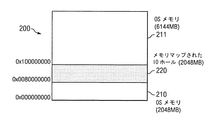
図2は、本発明の好ましい実施形態に係る、ホールをもつメモリアドレスをサポートするために仮想化することができる不連続物理メモリアドレス・スペースを有する、図1に示されるデータ処理システム100のローカルメモリ109のようなメモリデバイスの概略図である。説明に役立つ実例においては、メモリ200は、8ギガバイト(GB)、すなわち8192MBのシステムメモリを備える。システムメモリは、2つの不連続物理メモリ範囲に分割される。具体的には、メモリ200は、第1の物理範囲210及び第2の物理範囲211を含み、これらは、該第1の物理範囲210と該第2の物理範囲211との中間でアドレスホールを呈するメモリマップされた入力/出力(MMIO)物理範囲220によって分離されている。説明に役立つ実例においては、物理範囲210は、オペレーティング・システムによりアドレス可能な2048メガバイト(MB)のシステムメモリ範囲を含み、物理範囲211は、オペレーティング・システムによりアドレス可能な6144MBのシステムメモリ範囲を含む。物理範囲210は、16進法の0×000000000から0×07FFFFFFFまでの物理アドレス範囲を含み、物理範囲211は、16進法の0×100000000から0×15FFFFFFFまでの物理アドレス範囲を含む。キャッシュ禁止アドレスは、物理範囲210及び211の中間にアドレス範囲を有する物理範囲220にマップされる。このように、メモリ200は、物理範囲210及び211により与えられるシステムメモリの物理アドレスにおいて不連続性を呈するMMIO物理範囲220を含む。MMIO物理範囲220は、16進法の0×080000000から0×FFFFFFFFまでの物理メモリアドレス範囲を有する2048MBのメモリを備える。
FIG. 2 shows the locality of the
図3は、本発明の好ましい実施形態に係る、メモリホールをもつメモリアドレスをサポートするために、メモリアドレスの論理区画により仮想化を実現するソフトウェア及びハードウェア構成の概略図である。オペレーティング・システム304は、例えば、Linuxのオペレーティング・システムの実装、拡張対話式エグゼクティブ・オペレーティング・システム(AIX)といったUnix(登録商標)のオペレーティング・システムの別の変形その他同様なものとすることができる。オペレーティング・システム304は、アプリケーション302を稼動させる。論理区画(LPAR)管理306は、LPARリソースの管理を容易にするソフトウェアシステム層である。LPAR管理306は、例えば、ハードディスク又は図1に示されるデータ処理システム100のファームウェア115のようなシステムファームウェアに格納されるコンピュータプログラムとして維持されるコンピュータ実行可能命令を含むことができる。LPAR管理306は、例えば、ニューヨーク州アーモンク所在のインターナショナル・ビジネス・マシーンズ・コーポレーションの製品である、Hypervisorシステムとして実施することができる。LPAR管理306は、さらに、図1に示されるデータ処理システム100のローカルメモリ109のようなシステムメモリデバイスに割り振られたコンピュータ実行可能論理を含むことができる。例えば、LPAR管理306は、物理範囲210又は211の一部を、論理対物理アドレスのマッピング・テーブル、LPARプログラム及びデータ・ストレージその他同様なものに割り振ることができる。さらに、LPAR306は、オペレーティング・システム304の仮想アドレッシング・サポートを可能にするように、ページ・テーブルを割り振ることができる。マッピング・テーブル、ページ・テーブル、LPARプログラム及びデータ・ストレージにより利用される物理範囲210又は211のアドレス・スペースは、オペレーティング・システムによるアクセスには利用できない。
FIG. 3 is a schematic diagram of a software and hardware configuration that implements virtualization with logical partitioning of memory addresses to support memory addresses with memory holes, according to a preferred embodiment of the present invention. The
LPAR管理306は、プロセッサ308、及び、メモリ309、及び、入力及び出力(I/O)デバイス310といったシステムハードウェアに対するO/S304のアクセスを管理する。プロセッサ308は、図1に示されるデータ処理システム100のプロセッサ102及び104を表し、メモリ309は該データ処理システム100のローカルメモリ109を表す。プロセッサ308は、論理区画をサポートし、本発明の好ましい実装に係る論理区画環境の下で稼動するように構成される。
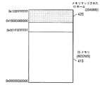
図4は、本発明の好ましい実施形態に係る、図1のデータ処理システム100のオペレーティング・システムに連続論理アドレス・スペースを与える、図3に示されるメモリ309のようなメモリデバイスの概略図である。MMIO物理範囲220の物理アドレスは、システムメモリをマッピングするのに要求されるあらゆる論理アドレスより上の論理アドレスに仮想化される。説明に役立つ実例においては、0×080000000から0×FFFFFFFFまでの物理アドレス範囲を有するMMIO物理範囲220は、0×10080000000から0×100FFFFFFFまでの論理アドレスを有する論理MMIO範囲420に仮想化される。さらに、O/S304には、0から物理メモリのサイズまでの論理アドレスを有するシステムメモリが提示される(LPAR管理306に要求されるどのようなオーバヘッドより少ない)。
4 is a schematic diagram of a memory device, such as the
例示的な実施においては、0×00000000000から0×001F5FFFFFFまでの論理アドレスを有する論理範囲410によりアクセスされるシステムメモリがO/S304に提示され、LPAR306プログラム、データ・ストレージ、及び論理対物理マッピング・テーブルは、32MBのシステムメモリを利用する。LPAR306は、仮想アドレスサポートのためにプロセッサ308により用いられるページ・テーブルに対して128MBのシステムメモリを使用する。このように、説明に役立つ実例においては、システムメモリは、0×00000000000から0×001F5FFFFFFまでの論理アドレスを含む論理範囲410によりアドレス指定される。MMIO物理範囲220は、0×10080000000から0×100FFFFFFFFまでの論理アドレスを含む論理MMIO範囲420によりアドレス指定される。
In an exemplary implementation, system memory accessed by logical range 410 having logical addresses from 0x00000000 to 0x001F5FFFFFF is presented to O /
LPAR管理306は、論理アドレスを対応する物理アドレスに変換して、物理メモリにアクセスする。例えば、変換は、論理範囲410に対してはテーブル索引により、及び論理MMIO範囲420に対しては範囲検査により行うことができる。本発明の好ましい実施形態に係るメモリアドレスの仮想化に対するマッピング・テーブルにより定義することができる、論理メモリの開始アドレス及び終了アドレス、及び、対応する物理メモリの開始アドレス及び終了アドレスは、以下の表1にまとめられている。表1に示されるように、論理MMIO範囲420の最下部又は開始アドレスは、論理範囲410の最上部又は終了アドレスより大きい。

図5は、本発明の好ましい実施形態に係る、オペレーティング・システムがホールをもつメモリアドレスをサポートするようにメモリデバイスを構成するための、図1のデータ処理システム100のようなデータ処理システムにより実行されるルーチンのフローチャートである。このルーチンは、例えば、システムのブート中に開始し(ステップ502)、データ処理システムのプロセッサが、論理区画環境において構成される(ステップ504)。物理範囲210のような物理メモリアドレスの第1の物理メモリアレイ又は範囲が、対応する第1の論理アドレス範囲又はアレイに仮想化される(ステップ506)。次に、物理範囲211のような、第1のメモリアレイと不連続である第2のメモリアレイが仮想化される(ステップ508)。第2の物理範囲の仮想化は、第2のメモリアレイに対応する仮想アドレス範囲が、第1のメモリアレイの仮想化により生成された論理アドレス範囲と連続するように実行される。このように、第1の及び第2の物理範囲の仮想化により生成された論理アドレス範囲は、連続する論理アドレス範囲をもたらす。
FIG. 5 is performed by a data processing system, such as
次に、MMIO物理アドレス範囲が、第3の論理アドレス範囲に仮想化される(ステップ510)。MMIO物理アドレス範囲の仮想化は、このMMIO物理アドレス範囲の仮想化により生成される論理アドレス範囲の最下部の論理アドレスが、物理範囲210及び211の仮想化により生成される論理アドレス範囲の最上部の論理アドレスよりも大きくなるように実行される。次に、マッピング・テーブルがシステムのメモリデバイスにロードされ、論理対物理アドレスの変換を与えて(ステップ512)、ルーチンは終了する(ステップ514)。従って、オペレーティング・システムには、システムメモリへのアクセスに対して、図4に示される論理範囲410のような単一の連続論理アドレス・スペースが提示されるという利点がある。
Next, the MMIO physical address range is virtualized to a third logical address range (step 510). In the virtualization of the MMIO physical address range, the lowest logical address of the logical address range generated by the virtualization of the MMIO physical address range is the uppermost part of the logical address range generated by the virtualization of the
このように、本発明はホールをもつシステムメモリアドレスをサポートするデータ処理システムを提供する。システムメモリの不連続物理アドレス範囲は、連続論理アドレス・スペースに仮想化される。メモリマップされた入力/出力物理範囲は、システムメモリの論理範囲の最上部アドレスの上に最下部のアドレスを有するメモリの論理範囲に仮想化される。有利なことに、ホールをもつシステムメモリアドレスをサポートするのに、データ処理システムのO/Sのカーネルの変更は必要ではない。 Thus, the present invention provides a data processing system that supports system memory addresses with holes. The discontinuous physical address range of system memory is virtualized into a continuous logical address space. The memory-mapped input / output physical range is virtualized to a logical range of memory having a bottom address above the top address of the logical range of system memory. Advantageously, no changes to the O / S kernel of the data processing system are required to support system memory addresses with holes.
本発明は、十分に機能するデータ処理システムとの関連において説明されてきたが、重要なこととして、当業者であれば、本発明のプロセスは、コンピュータ可読媒体の命令の形態、及び様々な形態で配布することができ、そして本発明は、この配布を行うために実際に用いられている特定形式の信号伝達媒体に係りなく、等しく適用可能であると認識するであろうことに注目するのは重要である。コンピュータ可読媒体の例には、フロッピー(登録商標)ディスク、ハードディスクドライブ、RAM、CD−ROM、DVD−ROMのような書き込み可能型媒体、例えば無線周波数及び光波伝送といった伝送形態を用いるデジタル及びアナログ通信リンク、有線又は無線通信リンクのような伝送型媒体がある。コンピュータ可読媒体は、特定のデータ処理システムにおける実際の使用のためにデコードされるコード化フォーマットの形態をとることができる。 Although the present invention has been described in the context of a well-functioning data processing system, it is important that those skilled in the art will understand that the process of the present invention is in the form of instructions and various forms of computer readable media. Note that the present invention will be equally applicable regardless of the particular type of signaling medium actually used to make this distribution. Is important. Examples of computer readable media include writable media such as floppy disks, hard disk drives, RAM, CD-ROMs, DVD-ROMs, digital and analog communications using transmission formats such as radio frequency and lightwave transmission. There are transmission-type media such as links, wired or wireless communication links. The computer readable medium may take the form of coded formats that are decoded for actual use in a particular data processing system.
本発明の詳細な説明は、図示及び説明のために与えられるものであって、網羅的なものとして、すなわち本発明を開示された形態に限定するものとして意図されたものではない。多くの修正及び変形が当業者には明らかとなるであろう。実施形態は、本発明の原理、実用的用途を最も良く解説し、かつ当業者以外の人が本発明の種々の修正を有する種々の実施形態を、考えられる特定の用途に適するものとして理解できるように、選択され、説明されるものである。 The detailed description of the present invention has been presented for purposes of illustration and description, and is not intended to be exhaustive or limited to the invention in the form disclosed. Many modifications and variations will be apparent to practitioners skilled in this art. The embodiments best explain the principles, practical applications of the invention, and those who are not skilled in the art can understand the various embodiments with various modifications of the invention as being suitable for the particular application envisaged. As such, it is selected and explained.
100:データ処理システム
102、104:プロセッサ
106:システムバス
108:メモリコントローラ/キャッシュ
109:ローカルメモリ
110:I/Oブリッジ
112:I/Oバス
114、122、124:PCIバスブリッジ
115:ファームウェア
116、126、128:PCIバス
118:モデム
120:ネットワーク・アダプタ
130:グラフィックス・アダプタ
132:ハードディスク
100:
Claims (20)
論理区画をサポートするように構成されたプロセッサにより稼動されるオペレーティング・システムのシステムメモリに対して割り振られた第1の物理アドレス範囲を仮想化して、第1の論理アドレス範囲を生成し、
前記オペレーティング・システムのシステムメモリに対して割り振られた、前記第1の物理アドレス範囲とは不連続の第2の物理アドレス範囲を仮想化して、前記第1の論理アドレス範囲に連続する第2の論理アドレス範囲を生成し、
前記第1及び第2の物理アドレス範囲の中間にあるメモリマップされた入力/出力物理アドレス範囲を仮想化して、第3の論理アドレス範囲を生成する、
ステップを含み、
前記第3の論理アドレス範囲の最下部の論理アドレスが、前記第1及び第2の論理アドレス範囲のそれぞれの最上部の論理アドレスを超えることを特徴とする方法。 A method for supporting memory addresses with holes, comprising steps implemented by a computer,
Virtualizing a first physical address range allocated to system memory of an operating system operated by a processor configured to support a logical partition to generate a first logical address range;
A second physical address range which is allocated to the system memory of the operating system and which is discontinuous with the first physical address range is virtualized, and the second logical address range is continuous with the first logical address range. Create a logical address range,
Virtualizing a memory-mapped input / output physical address range intermediate the first and second physical address ranges to generate a third logical address range;
Including steps,
The lowest logical address of the third logical address range exceeds the uppermost logical address of each of the first and second logical address ranges.
システムメモリに対して割り振られたメモリデバイスの第1及び第2の不連続物理アドレス範囲、及び、前記第1及び第2の物理アドレス範囲の中間にあるメモリマップされた入力/出力物理アドレス範囲を含む第3の物理アドレス範囲のための論理対物理メモリアドレス変換を格納する第1の命令を含み、前記論理対物理メモリアドレス変換により与えられる前記第3の物理アドレス範囲の最下部の論理アドレスが、該論理対物理メモリアドレス変換により与えられる、前記第1及び第2の不連続物理アドレス範囲に対応する前記第1及び第2の論理アドレス範囲の最上部より大きいものであり、
前記第1の命令の実行に応答して、論理アドレスを対応する物理アドレスに変換するための第2の命令、
を含むコンピュータプログラム。 A computer program in a computer readable medium for virtualizing a discontinuous physical memory range into a continuous logical address range, comprising:
A first and second discontinuous physical address range of memory devices allocated to system memory, and a memory mapped input / output physical address range intermediate the first and second physical address ranges; A first instruction storing a logical-to-physical memory address translation for a third physical address range that includes the logical address at the bottom of the third physical address range provided by the logical-to-physical memory address translation; Greater than the top of the first and second logical address ranges corresponding to the first and second discontinuous physical address ranges given by the logical-to-physical memory address translation,
A second instruction for translating a logical address into a corresponding physical address in response to execution of the first instruction;
A computer program containing
第1及び第2のそれぞれの物理アドレス範囲を有するシステムメモリに対して割り振られた第1及び第2の不連続物理メモリアレイと、前記第1及び第2の物理アドレス範囲の中間に第3の物理アドレス範囲を有する第3の物理メモリアレイと、データ・セットと、命令のセットとを含むメモリ、及び
論理区画をサポートするように構成されたプロセッサ、
を備え、前記プロセッサには、前記第1及び第2の不連続メモリアレイへのアクセスに対して、前記命令の実行に応答して、連続論理アドレス範囲が提示されることを特徴とするデータ処理システム。 A data processing system that supports a discontinuous system memory array,
A first and second discontinuous physical memory array allocated to system memory having first and second physical address ranges, and a third intermediate between the first and second physical address ranges. A memory configured to support a third physical memory array having a physical address range, a data set, a set of instructions, and a logical partition;
And the processor is presented with a continuous logical address range in response to execution of the instructions for accessing the first and second discontinuous memory arrays. system.
A second logical address range is mapped to the third physical address range, and the lowest logical address of the second logical address range is greater than the uppermost logical address of the continuous logical address range. The data processing system according to claim 15.
Applications Claiming Priority (1)
| Application Number | Priority Date | Filing Date | Title |
|---|---|---|---|
| US10/814,733 US7426625B2 (en) | 2004-03-31 | 2004-03-31 | Data processing system and computer program product for support of system memory addresses with holes |
Publications (2)
| Publication Number | Publication Date |
|---|---|
| JP2005293574A true JP2005293574A (en) | 2005-10-20 |
| JP4143616B2 JP4143616B2 (en) | 2008-09-03 |
Family
ID=35049895
Family Applications (1)
| Application Number | Title | Priority Date | Filing Date |
|---|---|---|---|
| JP2005076077A Expired - Fee Related JP4143616B2 (en) | 2004-03-31 | 2005-03-16 | Method and computer program for supporting memory addresses with holes |
Country Status (5)
| Country | Link |
|---|---|
| US (1) | US7426625B2 (en) |
| JP (1) | JP4143616B2 (en) |
| KR (1) | KR100773001B1 (en) |
| CN (1) | CN100385420C (en) |
| TW (1) | TWI340898B (en) |
Cited By (1)
| Publication number | Priority date | Publication date | Assignee | Title |
|---|---|---|---|---|
| JP2010186465A (en) * | 2008-12-08 | 2010-08-26 | Nvidia Corp | Centralized device virtualization layer for heterogeneous processing units |
Families Citing this family (18)
| Publication number | Priority date | Publication date | Assignee | Title |
|---|---|---|---|---|
| JP2007141066A (en) * | 2005-11-21 | 2007-06-07 | Toshiba Corp | Information processing apparatus and memory address space allocation method |
| US7685401B2 (en) * | 2006-12-27 | 2010-03-23 | Intel Corporation | Guest to host address translation for devices to access memory in a partitioned system |
| US8141093B2 (en) * | 2007-11-15 | 2012-03-20 | International Business Machines Corporation | Management of an IOV adapter through a virtual intermediary in an IOV management partition |
| CN101203019B (en) * | 2007-11-20 | 2011-01-05 | 中兴通讯股份有限公司 | Method and device for exchanging logical address and physical address of communication equipment |
| US8209554B2 (en) * | 2009-02-23 | 2012-06-26 | International Business Machines Corporation | Applying power management on a partition basis in a multipartitioned computer system |
| US9195581B2 (en) * | 2011-07-01 | 2015-11-24 | Apple Inc. | Techniques for moving data between memory types |
| US20130219146A1 (en) * | 2012-02-16 | 2013-08-22 | Micron Technology, Inc. | Method, device and system for a configurable address space for non-volatile memory |
| US20130219105A1 (en) * | 2012-02-16 | 2013-08-22 | Micron Technology, Inc. | Method, device and system for caching for non-volatile memory device |
| US20150310787A1 (en) * | 2013-10-21 | 2015-10-29 | Pixtronix, Inc. | Ems displays incorporating conductive edge seals and methods for manufacturing thereof |
| US10114752B2 (en) | 2014-06-27 | 2018-10-30 | International Business Machines Corporation | Detecting cache conflicts by utilizing logical address comparisons in a transactional memory |
| US20150378904A1 (en) * | 2014-06-27 | 2015-12-31 | International Business Machines Corporation | Allocating read blocks to a thread in a transaction using user specified logical addresses |
| US10095417B1 (en) * | 2016-12-13 | 2018-10-09 | EMC IP Holding Company LLC | Method and system for improving flash storage read performance in partially programmed blocks |
| US10289550B1 (en) | 2016-12-30 | 2019-05-14 | EMC IP Holding Company LLC | Method and system for dynamic write-back cache sizing in solid state memory storage |
| US10338983B2 (en) | 2016-12-30 | 2019-07-02 | EMC IP Holding Company LLC | Method and system for online program/erase count estimation |
| US11069418B1 (en) | 2016-12-30 | 2021-07-20 | EMC IP Holding Company LLC | Method and system for offline program/erase count estimation |
| US10403366B1 (en) | 2017-04-28 | 2019-09-03 | EMC IP Holding Company LLC | Method and system for adapting solid state memory write parameters to satisfy performance goals based on degree of read errors |
| US10290331B1 (en) | 2017-04-28 | 2019-05-14 | EMC IP Holding Company LLC | Method and system for modulating read operations to support error correction in solid state memory |
| US11099980B2 (en) * | 2018-05-09 | 2021-08-24 | International Business Machines Corporation | Host aware update write |
Family Cites Families (33)
| Publication number | Priority date | Publication date | Assignee | Title |
|---|---|---|---|---|
| JPH0658649B2 (en) * | 1985-10-28 | 1994-08-03 | 株式会社日立製作所 | Area management method in virtual memory device |
| JPS6419446U (en) | 1987-07-21 | 1989-01-31 | ||
| JPH0813814B2 (en) | 1988-10-18 | 1996-02-14 | ダイセル化学工業株式会社 | Process for producing fused heterocyclic compound |
| US5117350A (en) * | 1988-12-15 | 1992-05-26 | Flashpoint Computer Corporation | Memory address mechanism in a distributed memory architecture |
| JPH02189655A (en) | 1989-01-18 | 1990-07-25 | Fujitsu Ltd | Absolute address conversion system for information processor |
| US5297270A (en) * | 1989-11-13 | 1994-03-22 | Zenith Data Systems Corporation | Programmable cache memory which associates each section of main memory to be cached with a status bit which enables/disables the caching accessibility of the particular section, and with the capability of functioning with memory areas of varying size |
| JPH03288267A (en) | 1990-04-04 | 1991-12-18 | Toshiba Corp | Transmission system for medical image data |
| WO1994014119A1 (en) * | 1992-12-07 | 1994-06-23 | Raxco, Incorporated | Apparatus and method for moving open files |
| EP0608622A1 (en) * | 1993-01-29 | 1994-08-03 | International Business Machines Corporation | Multiprocessor system with multilevel caches |
| EP0610583A1 (en) | 1993-02-08 | 1994-08-17 | International Business Machines Corporation | Multizone relocation facility computer memory system |
| US5548746A (en) * | 1993-11-12 | 1996-08-20 | International Business Machines Corporation | Non-contiguous mapping of I/O addresses to use page protection of a process |
| JP3505231B2 (en) | 1994-09-30 | 2004-03-08 | 株式会社東芝 | Computer system |
| JP3540388B2 (en) | 1994-09-30 | 2004-07-07 | 株式会社東芝 | Computer system |
| SG45399A1 (en) | 1994-01-12 | 1998-01-16 | Sun Microsystems Inc | Logically addressable physical memory for a virtual memory computer system that support multiple page sizes |
| US5675761A (en) * | 1994-05-16 | 1997-10-07 | International Business Machines Corporation | Method and system for providing discontiguous drive support |
| JP3740195B2 (en) | 1994-09-09 | 2006-02-01 | 株式会社ルネサステクノロジ | Data processing device |
| US5581768A (en) * | 1995-02-27 | 1996-12-03 | Intel Corporation | Method and apparatus for executing applications in place from write once/seldom memories |
| US6256710B1 (en) * | 1995-04-28 | 2001-07-03 | Apple Computer, Inc. | Cache management during cache inhibited transactions for increasing cache efficiency |
| JPH0922377A (en) * | 1995-07-07 | 1997-01-21 | Ekushingu:Kk | Memory map address conversion circuit |
| US6061773A (en) * | 1996-05-03 | 2000-05-09 | Digital Equipment Corporation | Virtual memory system with page table space separating a private space and a shared space in a virtual memory |
| US5819298A (en) * | 1996-06-24 | 1998-10-06 | Sun Microsystems, Inc. | File allocation tables with holes |
| US5873124A (en) * | 1997-02-06 | 1999-02-16 | Microsoft Corporation | Virtual memory scratch pages |
| US5940868A (en) * | 1997-07-18 | 1999-08-17 | Digital Equipment Corporation | Large memory allocation method and apparatus |
| US6226730B1 (en) * | 1998-06-05 | 2001-05-01 | Intel Corporation | Achieving page hit memory cycles on a virtual address reference |
| JP2000347929A (en) | 1999-06-09 | 2000-12-15 | Nec Eng Ltd | Memory ic |
| US6629111B1 (en) * | 1999-10-13 | 2003-09-30 | Cisco Technology, Inc. | Memory allocation system |
| US6505269B1 (en) * | 2000-05-16 | 2003-01-07 | Cisco Technology, Inc. | Dynamic addressing mapping to eliminate memory resource contention in a symmetric multiprocessor system |
| US6877158B1 (en) * | 2000-06-08 | 2005-04-05 | International Business Machines Corporation | Logical partitioning via hypervisor mediated address translation |
| KR100392382B1 (en) * | 2001-07-27 | 2003-07-23 | 한국전자통신연구원 | Method of The Logical Volume Manager supporting Dynamic Online resizing and Software RAID |
| US6564299B1 (en) * | 2001-07-30 | 2003-05-13 | Lsi Logic Corporation | Method and apparatus for defining cacheable address ranges |
| US7055015B2 (en) * | 2002-02-25 | 2006-05-30 | Ricoh Company, Ltd. | Information processing apparatus in which processes can reduce overhead of memory access and efficiently share memory |
| US20030188062A1 (en) * | 2002-03-28 | 2003-10-02 | Luse Paul E. | Device resource allocation |
| US6904490B2 (en) * | 2002-10-10 | 2005-06-07 | International Business Machines Corporation | Method and system of managing virtualized physical memory in a multi-processor system |
-
2004
- 2004-03-31 US US10/814,733 patent/US7426625B2/en not_active Expired - Fee Related
-
2005
- 2005-02-18 CN CNB2005100093115A patent/CN100385420C/en not_active Expired - Fee Related
- 2005-03-10 TW TW094107357A patent/TWI340898B/en not_active IP Right Cessation
- 2005-03-16 JP JP2005076077A patent/JP4143616B2/en not_active Expired - Fee Related
- 2005-03-31 KR KR1020050027195A patent/KR100773001B1/en not_active Expired - Fee Related
Cited By (1)
| Publication number | Priority date | Publication date | Assignee | Title |
|---|---|---|---|---|
| JP2010186465A (en) * | 2008-12-08 | 2010-08-26 | Nvidia Corp | Centralized device virtualization layer for heterogeneous processing units |
Also Published As
| Publication number | Publication date |
|---|---|
| CN100385420C (en) | 2008-04-30 |
| JP4143616B2 (en) | 2008-09-03 |
| KR20060045387A (en) | 2006-05-17 |
| TW200602865A (en) | 2006-01-16 |
| CN1677370A (en) | 2005-10-05 |
| KR100773001B1 (en) | 2007-11-05 |
| US7426625B2 (en) | 2008-09-16 |
| US20050223185A1 (en) | 2005-10-06 |
| TWI340898B (en) | 2011-04-21 |
Similar Documents
| Publication | Publication Date | Title |
|---|---|---|
| JP4143616B2 (en) | Method and computer program for supporting memory addresses with holes | |
| US10423435B1 (en) | Page swapping in virtual machine environment | |
| JP4288295B2 (en) | Accessing memory in logical partitions | |
| JP6050262B2 (en) | Virtual disk storage technology | |
| US9183157B2 (en) | Method for creating virtual machine, a virtual machine monitor, and a virtual machine system | |
| US6877158B1 (en) | Logical partitioning via hypervisor mediated address translation | |
| US8533418B2 (en) | Memory allocation with identification of requesting loadable kernel module | |
| US8359449B2 (en) | Prioritizing virtual real memory paging based on disk capabilities | |
| EP2350833B1 (en) | Opportunistic page largification | |
| EP2581828B1 (en) | Method for creating virtual machine, virtual machine monitor and virtual machine system | |
| KR100992034B1 (en) | Computer Memory Management in Computing Environments with Dynamic Logical Partitioning | |
| US7506343B2 (en) | System and method for passing information from one device driver to another | |
| CN117743205A (en) | Method and apparatus for using DRAM as a buffer for byte addressable memory | |
| JP2004127291A (en) | Method, system, and computer software for offering successive memory address | |
| JP2024512960A (en) | System and method for providing page transitions | |
| US8612691B2 (en) | Assigning memory to on-chip coherence domains | |
| US20060010276A1 (en) | Isolation of input/output adapter direct memory access addressing domains | |
| US8375194B2 (en) | System and method for freeing memory | |
| JP4405435B2 (en) | Method and apparatus for dynamic host partition page allocation | |
| CN112817756B (en) | Computer readable storage medium, and virtualization method and device of memory management unit | |
| JP3808058B2 (en) | Apparatus for allowing a plurality of hosts to share a set of memory sectors storing compressed data | |
| CN114461391A (en) | A remappable GPU main memory access management method and system | |
| CN115934581B (en) | Method and system for processing cross-process memory | |
| US20070162638A1 (en) | Generic DMA memory space mapping | |
| HK1160944B (en) | Opportunistic page largification |
Legal Events
| Date | Code | Title | Description |
|---|---|---|---|
| A977 | Report on retrieval |
Free format text: JAPANESE INTERMEDIATE CODE: A971007 Effective date: 20080227 |
|
| A131 | Notification of reasons for refusal |
Free format text: JAPANESE INTERMEDIATE CODE: A131 Effective date: 20080311 |
|
| A521 | Request for written amendment filed |
Free format text: JAPANESE INTERMEDIATE CODE: A523 Effective date: 20080418 |
|
| TRDD | Decision of grant or rejection written | ||
| A01 | Written decision to grant a patent or to grant a registration (utility model) |
Free format text: JAPANESE INTERMEDIATE CODE: A01 Effective date: 20080610 |
|
| A01 | Written decision to grant a patent or to grant a registration (utility model) |
Free format text: JAPANESE INTERMEDIATE CODE: A01 |
|
| A61 | First payment of annual fees (during grant procedure) |
Free format text: JAPANESE INTERMEDIATE CODE: A61 Effective date: 20080616 |
|
| FPAY | Renewal fee payment (event date is renewal date of database) |
Free format text: PAYMENT UNTIL: 20110620 Year of fee payment: 3 |
|
| R150 | Certificate of patent or registration of utility model |
Free format text: JAPANESE INTERMEDIATE CODE: R150 |
|
| LAPS | Cancellation because of no payment of annual fees |