JP2005292685A - Liquid crystal device, projector and electronic device - Google Patents
Liquid crystal device, projector and electronic device Download PDFInfo
- Publication number
- JP2005292685A JP2005292685A JP2004110862A JP2004110862A JP2005292685A JP 2005292685 A JP2005292685 A JP 2005292685A JP 2004110862 A JP2004110862 A JP 2004110862A JP 2004110862 A JP2004110862 A JP 2004110862A JP 2005292685 A JP2005292685 A JP 2005292685A
- Authority
- JP
- Japan
- Prior art keywords
- liquid crystal
- crystal device
- water repellent
- layer
- light
- Prior art date
- Legal status (The legal status is an assumption and is not a legal conclusion. Google has not performed a legal analysis and makes no representation as to the accuracy of the status listed.)
- Granted
Links
- 239000004973 liquid crystal related substance Substances 0.000 title claims abstract description 132
- XLYOFNOQVPJJNP-UHFFFAOYSA-N water Substances O XLYOFNOQVPJJNP-UHFFFAOYSA-N 0.000 claims abstract description 77
- 239000005871 repellent Substances 0.000 claims abstract description 73
- 230000002940 repellent Effects 0.000 claims abstract description 58
- 239000000758 substrate Substances 0.000 claims abstract description 31
- 230000005684 electric field Effects 0.000 claims abstract description 5
- 229920001343 polytetrafluoroethylene Polymers 0.000 claims description 15
- 239000004810 polytetrafluoroethylene Substances 0.000 claims description 15
- 230000006866 deterioration Effects 0.000 abstract description 8
- 239000010408 film Substances 0.000 description 118
- 239000010410 layer Substances 0.000 description 103
- 238000013032 photocatalytic reaction Methods 0.000 description 16
- 239000003990 capacitor Substances 0.000 description 15
- 239000011229 interlayer Substances 0.000 description 12
- 239000004065 semiconductor Substances 0.000 description 12
- 238000010586 diagram Methods 0.000 description 11
- 239000000463 material Substances 0.000 description 9
- 229920001721 polyimide Polymers 0.000 description 8
- 238000003860 storage Methods 0.000 description 8
- 239000004642 Polyimide Substances 0.000 description 7
- 230000002542 deteriorative effect Effects 0.000 description 7
- 238000010521 absorption reaction Methods 0.000 description 6
- 239000011368 organic material Substances 0.000 description 6
- 239000004020 conductor Substances 0.000 description 5
- 229910010272 inorganic material Inorganic materials 0.000 description 5
- 239000011147 inorganic material Substances 0.000 description 5
- 230000015572 biosynthetic process Effects 0.000 description 4
- 239000011159 matrix material Substances 0.000 description 4
- 230000001681 protective effect Effects 0.000 description 4
- 238000004519 manufacturing process Methods 0.000 description 3
- YCKRFDGAMUMZLT-UHFFFAOYSA-N Fluorine atom Chemical compound [F] YCKRFDGAMUMZLT-UHFFFAOYSA-N 0.000 description 2
- 239000004988 Nematic liquid crystal Substances 0.000 description 2
- 238000000151 deposition Methods 0.000 description 2
- 239000007772 electrode material Substances 0.000 description 2
- 229910052731 fluorine Inorganic materials 0.000 description 2
- 239000011737 fluorine Substances 0.000 description 2
- 239000011521 glass Substances 0.000 description 2
- 125000002887 hydroxy group Chemical group [H]O* 0.000 description 2
- 238000000034 method Methods 0.000 description 2
- 230000003287 optical effect Effects 0.000 description 2
- 229910021420 polycrystalline silicon Inorganic materials 0.000 description 2
- -1 polytetrafluoroethylene Polymers 0.000 description 2
- 230000008569 process Effects 0.000 description 2
- 239000010453 quartz Substances 0.000 description 2
- 230000001105 regulatory effect Effects 0.000 description 2
- 239000000565 sealant Substances 0.000 description 2
- VYPSYNLAJGMNEJ-UHFFFAOYSA-N silicon dioxide Inorganic materials O=[Si]=O VYPSYNLAJGMNEJ-UHFFFAOYSA-N 0.000 description 2
- 239000002904 solvent Substances 0.000 description 2
- 238000004528 spin coating Methods 0.000 description 2
- 229920002396 Polyurea Polymers 0.000 description 1
- 239000004809 Teflon Substances 0.000 description 1
- 229920006362 Teflon® Polymers 0.000 description 1
- 239000002253 acid Substances 0.000 description 1
- 230000008901 benefit Effects 0.000 description 1
- 230000001413 cellular effect Effects 0.000 description 1
- 230000008859 change Effects 0.000 description 1
- 238000006243 chemical reaction Methods 0.000 description 1
- 239000003795 chemical substances by application Substances 0.000 description 1
- 150000004985 diamines Chemical class 0.000 description 1
- 230000000694 effects Effects 0.000 description 1
- 238000003682 fluorination reaction Methods 0.000 description 1
- 239000012535 impurity Substances 0.000 description 1
- AMGQUBHHOARCQH-UHFFFAOYSA-N indium;oxotin Chemical compound [In].[Sn]=O AMGQUBHHOARCQH-UHFFFAOYSA-N 0.000 description 1
- 239000007791 liquid phase Substances 0.000 description 1
- 230000007257 malfunction Effects 0.000 description 1
- 229910001507 metal halide Inorganic materials 0.000 description 1
- 150000005309 metal halides Chemical class 0.000 description 1
- 230000004048 modification Effects 0.000 description 1
- 238000012986 modification Methods 0.000 description 1
- 239000005416 organic matter Substances 0.000 description 1
- FYJQJMIEZVMYSD-UHFFFAOYSA-N perfluoro-2-butyltetrahydrofuran Chemical compound FC(F)(F)C(F)(F)C(F)(F)C(F)(F)C1(F)OC(F)(F)C(F)(F)C1(F)F FYJQJMIEZVMYSD-UHFFFAOYSA-N 0.000 description 1
- 230000002093 peripheral effect Effects 0.000 description 1
- 238000009832 plasma treatment Methods 0.000 description 1
- 229920000642 polymer Polymers 0.000 description 1
- 229920005591 polysilicon Polymers 0.000 description 1
- 230000000630 rising effect Effects 0.000 description 1
- 238000007789 sealing Methods 0.000 description 1
- 239000003566 sealing material Substances 0.000 description 1
- 239000010409 thin film Substances 0.000 description 1
- 238000001771 vacuum deposition Methods 0.000 description 1
Images


Landscapes
- Liquid Crystal (AREA)
- Devices For Indicating Variable Information By Combining Individual Elements (AREA)
Abstract
【課題】 配向膜の劣化を防止することが可能な液晶装置を提供する。
【解決手段】 一対の基板10,20により液晶層50が挟持された液晶装置60であって、液晶層50に電界を印加する透明電極9,21の表面に撥水層80,90を形成し、その撥水層80,90の表面に、液晶層50の液晶分子を配向させる有機配向膜16,22を形成した。なお撥水層80,90の表面に、親水処理が施されていることが望ましい。
【選択図】 図4PROBLEM TO BE SOLVED: To provide a liquid crystal device capable of preventing deterioration of an alignment film.
SOLUTION: A liquid crystal device 60 in which a liquid crystal layer 50 is sandwiched between a pair of substrates 10 and 20, and water repellent layers 80 and 90 are formed on the surfaces of transparent electrodes 9 and 21 for applying an electric field to the liquid crystal layer 50. The organic alignment films 16 and 22 for aligning the liquid crystal molecules of the liquid crystal layer 50 were formed on the surfaces of the water repellent layers 80 and 90. It is desirable that the surface of the water repellent layers 80 and 90 is subjected to a hydrophilic treatment.
[Selection] Figure 4
Description
本発明は、液晶装置、プロジェクタおよび電子機器に関するものである。 The present invention relates to a liquid crystal device, a projector, and an electronic apparatus.
液晶プロジェクタ等の投射型表示装置における光変調手段として、液晶装置が用いられている。液晶装置は、一対の基板により液晶層を挟持して構成されている。その一対の基板の液晶層側には、液晶層に対して電界を印加する電極が形成されている。この電極は、ITO等の透明導電性材料で構成されている。その電極の上層側には、液晶分子の配向状態を規制する配向膜が形成されている。この配向膜は、ポリイミド等の有機材料で構成されている。 A liquid crystal device is used as light modulation means in a projection display device such as a liquid crystal projector. A liquid crystal device is configured by sandwiching a liquid crystal layer between a pair of substrates. Electrodes for applying an electric field to the liquid crystal layer are formed on the liquid crystal layer side of the pair of substrates. This electrode is made of a transparent conductive material such as ITO. An alignment film that regulates the alignment state of the liquid crystal molecules is formed on the upper layer side of the electrode. This alignment film is made of an organic material such as polyimide.
液晶プロジェクタでは、光源から照射された光が光変調手段である液晶装置に入射する。そして、液晶装置における非選択電圧印加時と選択電圧印加時との液晶分子の配向変化に基づいて、光源光が変調される。これにより、画像光が形成されて、スクリーン上に拡大投射されるようになっている。
しかしながら、有機材料からなる配向膜や液晶層の内部には、微量の水分が含まれている。また、一対の基板を連結するシール剤を通して、液晶層の内部に水分が浸入する場合がある。これらの水分が透明電極の表面に付着した状態で、光源から照射された波長400〜450nm程度の光が液晶装置に導入されると、透明電極が光触媒反応を起して、非常に反応性の高いヒドロキシラジカルを発生させる。このヒドロキシラジカルにより、透明電極の表面に形成された有機配向膜が分解されるという問題がある。これに伴って、液晶分子を配向規制することが不可能になり、表示品質が悪化して、液晶プロジェクタの信頼性を低下させることになる。 However, a trace amount of moisture is contained in the alignment film or the liquid crystal layer made of an organic material. In some cases, moisture enters the liquid crystal layer through a sealant that connects the pair of substrates. When light having a wavelength of about 400 to 450 nm irradiated from a light source is introduced into the liquid crystal device in a state where these moistures are attached to the surface of the transparent electrode, the transparent electrode causes a photocatalytic reaction, which is very reactive. Generate high hydroxyl radicals. There is a problem that the organic alignment film formed on the surface of the transparent electrode is decomposed by the hydroxy radical. Along with this, it becomes impossible to regulate the alignment of the liquid crystal molecules, the display quality is deteriorated, and the reliability of the liquid crystal projector is lowered.
なお、特許文献1および特許文献2には、液晶装置の透明電極上に無機材料からなる保護膜を設ける構成が記載されている。しかしながら、無機材料には撥水効果がなく、水分に起因した配向膜の劣化を防止することは困難である。
本発明は、上記課題を解決するためになされたものであり、配向膜の劣化を防止することが可能な液晶装置の提供を目的とする。
また、信頼性に優れたプロジェクタおよび電子機器の提供を目的とする。
SUMMARY An advantage of some aspects of the invention is to provide a liquid crystal device capable of preventing the alignment film from being deteriorated.
It is another object of the present invention to provide a highly reliable projector and electronic device.
上記目的を達成するため、本発明の液晶装置は、一対の基板により液晶層が挟持された液晶装置であって、前記一対の基板の少なくとも一方の基板に形成され前記液晶層に電界を印加する透明導電膜の表面に、撥水層が形成されていることを特徴とする。
そして、前記撥水層の表面に、前記液晶層の液晶分子を配向させる有機配向膜が形成されていることが望ましい。
この構成によれば、透明導電膜の表面に撥水層が形成されているので、透明導電膜に対する水分の付着を防止することが可能になり、光触媒反応によるヒドロキシラジカルの発生を防止することができる。また、撥水層の表面に有機配向膜が形成されているので、ヒドロキシラジカルに起因する配向膜の劣化を防止することができる。
In order to achieve the above object, a liquid crystal device of the present invention is a liquid crystal device in which a liquid crystal layer is sandwiched between a pair of substrates, which is formed on at least one of the pair of substrates and applies an electric field to the liquid crystal layer. A water repellent layer is formed on the surface of the transparent conductive film.
It is desirable that an organic alignment film for aligning the liquid crystal molecules of the liquid crystal layer is formed on the surface of the water repellent layer.
According to this configuration, since the water repellent layer is formed on the surface of the transparent conductive film, it is possible to prevent moisture from adhering to the transparent conductive film, and to prevent generation of hydroxy radicals due to photocatalytic reaction. it can. Moreover, since the organic alignment film is formed on the surface of the water repellent layer, it is possible to prevent the alignment film from being deteriorated due to hydroxy radicals.
また、前記撥水層の表面に、親水処理が施されていることが望ましい。
この構成によれば、撥水層に対する有機配向膜の密着性を向上させて、有機配向膜の剥がれによる劣化を防止することができる。
Moreover, it is desirable that the surface of the water repellent layer be subjected to a hydrophilic treatment.
According to this configuration, the adhesion of the organic alignment film to the water repellent layer can be improved, and deterioration due to peeling of the organic alignment film can be prevented.
また、前記撥水層と、前記液晶層の液晶分子を配向させる有機配向膜との間に、表面エネルギが前記撥水層より小さく前記有機配向膜より大きい密着層が形成されていることが望ましい。
一般に、隣接する膜の表面エネルギ差を小さくすることにより密着性が向上するので、表面エネルギが撥水層より小さく有機配向膜より大きい密着層を形成することにより、撥水層に対する有機配向膜の密着性を向上させることができる。これにより、有機配向膜の剥がれによる劣化を防止することができる。
Further, it is desirable that an adhesion layer having a surface energy smaller than that of the water repellent layer and larger than that of the organic alignment film is formed between the water repellent layer and the organic alignment film that aligns liquid crystal molecules of the liquid crystal layer. .
In general, the adhesiveness is improved by reducing the surface energy difference between adjacent films. Therefore, by forming an adhesion layer whose surface energy is smaller than the water repellent layer and larger than the organic alignment film, Adhesion can be improved. Thereby, deterioration due to peeling of the organic alignment film can be prevented.
また、前記撥水層が、前記液晶層の液晶分子を配向させる配向膜として機能することが望ましい。
この構成によれば、別途配向膜を形成する必要がないので、液晶装置の製造コストを低減することができる。また、吸水性が低く酸化されにくい撥水層によって配向膜を構成することにより、配向膜の劣化を防止することができる。
Moreover, it is desirable that the water repellent layer functions as an alignment film for aligning the liquid crystal molecules of the liquid crystal layer.
According to this configuration, it is not necessary to separately form an alignment film, so that the manufacturing cost of the liquid crystal device can be reduced. Further, the alignment film can be prevented from being deteriorated by forming the alignment film with a water-repellent layer that has low water absorption and is not easily oxidized.
また、前記撥水層は、PTFEからなることが望ましい。
構造的に安定したPTFEによって撥水層を形成すれば、長期間にわたって透明導電膜に対する水分の付着を防止することが可能になり、配向膜の劣化を防止することができる。特に、PTFEによって形成された撥水層を配向膜として機能させれば、長期間にわたって配向膜の劣化を防止することができる。
The water repellent layer is preferably made of PTFE.
If the water-repellent layer is formed by structurally stable PTFE, it becomes possible to prevent moisture from adhering to the transparent conductive film over a long period of time, and to prevent deterioration of the alignment film. In particular, if a water repellent layer formed of PTFE is allowed to function as an alignment film, the alignment film can be prevented from deteriorating over a long period of time.
一方、本発明のプロジェクタは、上述した液晶装置を光変調手段として採用したことを特徴とする。
プロジェクタの光変調手段には光源から照射された強い光が入射するが、上述した液晶装置は配向膜の劣化を防止することができるので、長期間にわたって液晶装置を光変調手段として機能させることができる。したがって、信頼性に優れたプロジェクタを提供することができる。
On the other hand, the projector of the present invention is characterized in that the above-described liquid crystal device is employed as the light modulation means.
Although strong light emitted from the light source is incident on the light modulation means of the projector, the liquid crystal device described above can prevent the alignment film from deteriorating, so that the liquid crystal device can function as the light modulation means for a long period of time. it can. Therefore, a projector having excellent reliability can be provided.
一方、本発明の電子機器は、上述した液晶装置を備えたことを特徴とする。
この構成によれば、信頼性に優れた電子機器を提供することができる。
On the other hand, an electronic apparatus according to the present invention includes the above-described liquid crystal device.
According to this configuration, an electronic device with excellent reliability can be provided.
以下、本発明の実施形態につき、図面を参照して説明する。なお、以下の説明に用いる各図面では、各部材を認識可能な大きさとするため、各部材の縮尺を適宜変更している。なお本明細書では、液晶装置の各構成部材における液晶層側を内側と呼び、その反対側を外側と呼ぶことにする。また、「非選択電圧印加時」および「選択電圧印加時」とは、それぞれ「液晶層への印加電圧が液晶の配向が変化するしきい値電圧近傍である時」および「液晶層への印加電圧が液晶のしきい値電圧に比べて十分高い時」を意味しているものとする。 Embodiments of the present invention will be described below with reference to the drawings. In each drawing used for the following description, the scale of each member is appropriately changed to make each member a recognizable size. In the present specification, the liquid crystal layer side of each component of the liquid crystal device is referred to as an inner side, and the opposite side is referred to as an outer side. “When non-selection voltage is applied” and “when selection voltage is applied” are respectively “when the applied voltage to the liquid crystal layer is near the threshold voltage at which the liquid crystal orientation changes” and “applied to the liquid crystal layer”. "When the voltage is sufficiently higher than the threshold voltage of the liquid crystal".
[第1実施形態]
最初に、本発明の第1実施形態に係る液晶装置につき、図1ないし図4を用いて説明する。図4に示すように、第1実施形態に係る液晶装置60は、一対の基板10A,20Aにより液晶層50が挟持され、その液晶層50に電界を印加する電極9,21の表面に、撥水層80,90が形成されているものである。なお本実施形態では、スイッチング素子として薄膜トランジスタ(Thin Film Transistor、以下TFTという)素子を用いたアクティブマトリクス方式の透過型液晶装置を例にして説明する。
[First Embodiment]
First, a liquid crystal device according to a first embodiment of the present invention will be described with reference to FIGS. As shown in FIG. 4, in the
(等価回路)
図1は、液晶装置の等価回路図である。透過型液晶装置の画像表示領域を構成すべくマトリクス状に配置された複数のドットには、画素電極9が形成されている。また、その画素電極9の側方には、当該画素電極9への通電制御を行うためのスイッチング素子であるTFT素子30が形成されている。このTFT素子30のソースには、データ線6aが電気的に接続されている。その各データ線6aには、画像信号S1、S2、…、Snが供給されるようになっている。なお画像信号S1、S2、…、Snは、各データ線6aに対してこの順に線順次で供給してもよく、相隣接する複数のデータ線6aに対してグループ毎に供給してもよい。
(Equivalent circuit)
FIG. 1 is an equivalent circuit diagram of the liquid crystal device.
また、TFT素子30のゲートには、走査線3aが電気的に接続されている。走査線3aには、所定のタイミングでパルス的に走査信号G1、G2、…、Gmが供給されるようになっている。なお走査信号G1、G2、…、Gmは、各走査線3aに対してこの順に線順次で印加する。また、TFT素子30のドレインには、画素電極9が電気的に接続されている。そして、走査線3aから供給された走査信号G1、G2、…、Gmにより、スイッチング素子であるTFT素子30を一定期間だけオン状態にすると、データ線6aから供給された画像信号S1、S2、…、Snが、各画素の液晶に所定のタイミングで書き込まれるようになっている。
The
液晶に書き込まれた所定レベルの画像信号S1、S2、…、Snは、画素電極9と後述する共通電極との間に形成される液晶容量で一定期間保持される。なお、保持された画像信号S1、S2、…、Snがリークするのを防止するため、画素電極9と容量線3bとの間に蓄積容量17が形成され、液晶容量と並列に配置されている。このように、液晶に電圧信号が印加されると、印加された電圧レベルにより液晶分子の配向状態が変化する。これにより、液晶に入射した光が変調されて、階調表示ができるようになっている。
The predetermined level image signals S1, S2,..., Sn written in the liquid crystal are held for a certain period by a liquid crystal capacitor formed between the
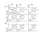
(平面構造)
図2は、液晶装置の平面構造の説明図である。本実施形態の液晶装置では、TFTアレイ基板上に、矩形状の画素電極9(破線9aによりその輪郭を示す)がマトリクス状に配列形成されている。また、画素電極9の縦横の境界に沿って、データ線6a、走査線3aおよび容量線3bが設けられている。本実施形態では、各画素電極9の形成された領域がドット領域であり、マトリクス状に配置されたドット領域ごとに表示を行うことができるようになっている。
(Planar structure)
FIG. 2 is an explanatory diagram of a planar structure of the liquid crystal device. In the liquid crystal device of this embodiment, rectangular pixel electrodes 9 (the outline of which are indicated by
TFT素子30は、ポリシリコン膜等からなる半導体層1aを中心として形成されている。半導体層1aのソース領域(後述)には、コンタクトホール5を介して、データ線6aが電気的に接続されている。また、半導体層1aのドレイン領域(後述)には、コンタクトホール8を介して、画素電極9が電気的に接続されている。一方、半導体層1aにおける走査線3aとの対向部分には、チャネル領域1a’が形成されている。なお走査線3aは、チャネル領域1a’との対向部分においてゲート電極として機能する。
The
容量線3bは、走査線3aに沿って略直線状に伸びる本線部(すなわち平面的に見て、走査線3aに沿って形成された第1領域)と、データ線6aとの交点からデータ線6aに沿って前段側(図中上向き)に突出した突出部(すなわち平面的に見て、データ線6aに沿って延設された第2領域)とによって構成されている。また、図2中に右上がりの斜線で示した領域には、第1遮光膜11aが形成されている。そして、容量線3bの突出部と第1遮光膜11aとがコンタクトホール13を介して電気的に接続され、後述する蓄積容量が形成されている。
The
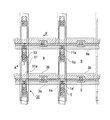
(断面構造)
図3は、液晶装置の断面構造の説明図であり、図2のA−A’線における側面断面図である。図3に示すように、本実施形態の液晶装置60は、TFTアレイ基板10と、これに対向配置された対向基板20と、これらの間に挟持された液晶層50とを主体として構成されている。TFTアレイ基板10は、ガラスや石英等の透光性材料からなる基板本体10A、およびその内側に形成されたTFT素子30や画素電極9、配向膜16などを主体として構成されている。一方の対向基板20は、ガラスや石英等の透光性材料からなる基板本体20A、およびその内側に形成された共通電極21や配向膜22などを主体として構成されている。
(Cross-section structure)
3 is an explanatory diagram of a cross-sectional structure of the liquid crystal device, and is a side cross-sectional view taken along the line AA ′ of FIG. As shown in FIG. 3, the
TFTアレイ基板10の表面には、後述する第1遮光膜11aおよび第1層間絶縁膜12が形成されている。そして、第1層間絶縁膜12の表面には多結晶シリコン等からなる半導体層1aが形成され、この半導体層1aを中心としてTFT素子30が形成されている。半導体層1aにおける走査線3aとの対向部分にはチャネル領域1a’が形成され、その両側にソース領域およびドレイン領域が形成されている。なお、このTFT素子30はLDD(Lightly Doped Drain)構造を採用しているため、ソース領域およびドレイン領域に、それぞれ不純物濃度が相対的に高い高濃度領域と、相対的に低い低濃度領域(LDD領域)とが形成されている。すなわち、ソース領域には低濃度ソース領域1bと高濃度ソース領域1dとが形成され、ドレイン領域には低濃度ドレイン領域1cと高濃度ドレイン領域1eとが形成されている。
On the surface of the
半導体層1aの表面には、ゲート絶縁膜2が形成されている。そして、ゲート絶縁膜2の表面に走査線3aが形成されて、その一部がゲート電極を構成している。また、ゲート絶縁膜2および走査線3aの表面には、第2層間絶縁膜4が形成されている。そして、第2層間絶縁膜4の表面にデータ線6aが形成され、第2層間絶縁膜4に形成されたコンタクトホール5を介して、高濃度ソース領域1dと電気的に接続されている。さらに、第2層間絶縁膜4およびデータ線6aの表面には、第3層間絶縁膜7が形成されている。そして、第3層間絶縁膜7の表面には、インジウム錫酸化物(Indium Tin Oxide、以下ITOという)等の透明導電性材料からなる画素電極9が形成されている。この画素電極9は、第2層間絶縁膜4および第3層間絶縁膜7に形成されたコンタクトホール8を介して、高濃度ドレイン領域1eと電気的に接続されている。さらに、画素電極9の内側には、後述する撥水層(不図示)を介して、ポリイミド等の有機材料からなる配向膜16が形成されている。配向膜16の表面にはラビング等が施され、非選択電圧印加時における液晶分子の配向方向を規制しうるようになっている。
A
なお、本実施形態では、半導体層1aを延設して第1蓄積容量電極1fが形成されている。また、ゲート絶縁膜2を延設して誘電体膜が形成され、その表面に容量線3bが配置されて第2蓄積容量電極が形成されている。これらにより、上述した蓄積容量17が構成されている。
In the present embodiment, the first
また、TFT素子30の形成領域に対応するTFTアレイ基板10の表面に、第1遮光膜11aが形成されている。第1遮光膜11aは、液晶装置に入射した光が、半導体層1aのチャネル領域1a'、低濃度ソース領域1bおよび低濃度ドレイン領域1cに侵入することを防止するものである。なお、第1遮光膜11aは、第1層間絶縁膜12に形成されたコンタクトホール13を介して、前段あるいは後段の容量線3bと電気的に接続されている。これにより、第1遮光膜11aは第3蓄積容量電極として機能し、第1層間絶縁膜12を誘電体膜として、第1蓄積容量電極1fとの間に新たな蓄積容量が形成されている。
The first
一方、データ線6a、走査線3aおよびTFT素子30の形成領域に対応する対向基板20の表面には、第2遮光膜23が形成されている。第2遮光膜23は、液晶装置に入射した光が、半導体層1aのチャネル領域1a’や低濃度ソース領域1b、低濃度ドレイン領域1cに侵入するのを防止するものである。また、対向基板20および第2遮光膜23の表面には、ほぼ全面にわたってITO等の透明導電性材料からなる共通電極21が形成されている。さらに、共通電極21の表面には、後述する撥水層(不図示)を介して、ポリイミド等の有機材料からなる配向膜22が形成されている。配向膜22の表面にはラビング等が施され、非選択電圧印加時における液晶分子の配向方向を規制しうるようになっている。
On the other hand, a second
配向膜16,22を形成するには、まずポリイミドをスピンコートにより塗布し、約80℃で10分間程度乾燥させて溶剤を揮発させた後に、約180℃で1時間程度焼成して、ポリイミド膜を形成する。さらに、そのポリイミド膜をラビング密度450程度でラビング処理すれば、配向膜16,22が形成される。一例を挙げれば、配向膜16,22の厚さは、約250オングストロームに形成されている。なお、配向膜16,22の厚さは50〜500オングストロームとすることが好ましく、150〜300オングストロームとすることがより好ましい。
In order to form the
そして、TFTアレイ基板10および対向基板20を周縁部で接着するシール剤の内側には、ネマチック液晶からなる液晶層50が封止されている。このネマチック液晶分子は、正の誘電率異方性を示すものであり、非選択電圧印加時には電極に対して水平に配向し、選択電圧印加時には電極に対して垂直に配向するようになっている。なお、TFTアレイ基板10の配向膜16による配向規制方向と、対向基板20の配向膜22による配向規制方向とは、約90°ねじれた状態で配置されている。これにより、本実施形態の液晶装置60は、ツイステッドネマチックモードで動作するようになっている。
A
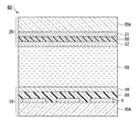
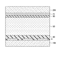
(撥水層)
図4は、本実施形態に係る液晶装置の説明図である。なお図4は、図3に示す断面構造の概略図であり、理解を容易にするためTFT素子等の記載が省略されている。
図4に示すように、本実施形態に係る液晶装置60では、ITO等の透明導電性材料からなる画素電極9および共通電極21の表面を覆うように、それぞれ撥水層80,90が形成されている。そして、これら撥水層80,90の表面に、ポリイミド等の有機材料からなる配向膜16,22がそれぞれ形成されている。これらの撥水層80,90は、フッ素系高分子等の撥水性を有する材料により、10〜100nm程度の厚さに形成されている。
(Water repellent layer)
FIG. 4 is an explanatory diagram of the liquid crystal device according to the present embodiment. FIG. 4 is a schematic diagram of the cross-sectional structure shown in FIG. 3, and description of TFT elements and the like is omitted for easy understanding.
As shown in FIG. 4, in the
具体的には、平均分子量1000〜10000のPTFE(ポリテトラフルオロエチレン)を電極9,21の表面に真空蒸着させることによって、撥水層80,90を形成することが望ましい。構造的に安定したPTFEによって撥水層を形成すれば、長期間にわたって撥水性能を発揮することができる。なお、テフロンAF(登録商標)をフッ素系溶剤(例えばフロリナートFC−75)に溶解したものを、電極9,21の表面にスピンコートすることによって、撥水層80,90を形成することも可能である。この場合には、液相プロセスによって撥水層が形成されるので、製造コストを低減することができる。
Specifically, it is desirable to form the water repellent layers 80 and 90 by vacuum-depositing PTFE (polytetrafluoroethylene) having an average molecular weight of 1000 to 10,000 on the surfaces of the
ところで、ITO等の透明な電極材料は、導電体と半導体との中間的な性質を有する。この電極材料に対して吸収波長近傍の光を照射すると、光触媒反応が起こる。そして、水分の存在下で光触媒反応が起こると、ヒドロキシラジカルが発生する。このヒドロキシラジカルは非常に反応性が高く、有機物を分解する性質を有する。
液晶装置では、配向膜16,22や液晶層50等の内部に含まれていた水分や、外部からシール剤を透過して侵入した水分が、透明電極9,21に付着する場合がある。この状態で、ITOの吸収波長である350nm近傍の光が透明電極9,21に入射すると、光触媒反応によりヒドロキシラジカルが発生する。このヒドロキシラジカルにより、ポリイミド等の有機材料からなる配向膜16,22が分解されるおそれがある。そして配向膜16,22が分解されると、液晶分子の配向規制が不能になり、画像光を形成することができなくなる。
By the way, a transparent electrode material such as ITO has an intermediate property between a conductor and a semiconductor. When this electrode material is irradiated with light in the vicinity of the absorption wavelength, a photocatalytic reaction occurs. When a photocatalytic reaction occurs in the presence of moisture, a hydroxy radical is generated. This hydroxy radical is very reactive and has the property of decomposing organic matter.
In the liquid crystal device, moisture contained in the
これに対して、本実施形態の液晶装置では、透明電極9,21の表面に撥水層80,90が形成されている。この撥水層80,90により、透明電極9,21の表面に対する水分の付着を防止することができる。これに伴って、光触媒反応によるヒドロキシラジカルの発生を防止することが可能になり、配向膜の劣化を防止することができる。したがって、液晶装置の信頼性を向上させることが可能になる。一例を挙げれば、撥水層を形成しない従来の液晶装置と比べて、液晶装置の信頼性(表示品質が低下するまでの時間)を1.5倍程度に向上させることができる。
On the other hand, in the liquid crystal device of the present embodiment, the water repellent layers 80 and 90 are formed on the surfaces of the
また、本実施形態の液晶装置では、前記撥水層をPTFEによって形成した。構造的に安定したPTFEによって撥水層を形成すれば、長期間にわたって透明導電膜に対する水分の付着を防止することが可能になり、配向膜の劣化を防止することができる。また、液晶装置をプロジェクタの光変調手段(ライトバルブ)として使用した場合でも、光源からの強い光によって分解されるおそれが少なくなり、長期間にわたって撥水性能を発揮することができる。加えて、平均分子量1000〜10000のPTFEを採用することにより、PTFEの真空蒸着を可能としつつ、良好な撥水性能を発揮することができる。 Further, in the liquid crystal device of the present embodiment, the water repellent layer is formed by PTFE. If the water-repellent layer is formed by structurally stable PTFE, it becomes possible to prevent moisture from adhering to the transparent conductive film over a long period of time, and to prevent deterioration of the alignment film. Further, even when the liquid crystal device is used as a light modulation means (light valve) of a projector, there is less possibility of being decomposed by strong light from the light source, and water repellency can be exhibited over a long period of time. In addition, by adopting PTFE having an average molecular weight of 1000 to 10,000, it is possible to exhibit good water repellency while enabling vacuum deposition of PTFE.
なお、透明電極の表面に無機材料からなる保護膜を設ける構成が知られている。この無機材料として、遮水性(水分の非透過性)を有するものを採用することにより、透明電極の表面に対する水分の付着を防止することも考えられる。しかしながら、無機材料からなる保護膜の表面に配向膜を形成すると、保護膜表面の水酸基と配向膜とが反応して、配向膜を劣化させるという問題がある。これに対して、本実施形態のように撥水層の表面に配向膜を形成すれば、水酸基により配向膜を劣化させることはない。また、撥水層を形成することにより、遮水層より効果的に、透明電極に対する水分の付着を防止することが可能になる。 In addition, the structure which provides the protective film which consists of inorganic materials on the surface of a transparent electrode is known. As this inorganic material, it is conceivable to prevent water from adhering to the surface of the transparent electrode by adopting a material having water shielding properties (water impermeability). However, when an alignment film is formed on the surface of the protective film made of an inorganic material, there is a problem that the hydroxyl group on the surface of the protective film reacts with the alignment film to deteriorate the alignment film. On the other hand, if the alignment film is formed on the surface of the water repellent layer as in this embodiment, the alignment film is not deteriorated by the hydroxyl group. Moreover, by forming the water repellent layer, it becomes possible to prevent moisture from adhering to the transparent electrode more effectively than the water shielding layer.
以上には、撥水性を有する材料により撥水層を形成する構成について説明したが、透明電極の表面に形成された撥水性を有しない材料層の表面を撥水処理することによって、撥水層を形成することも可能である。具体的には、撥水処理として、CF4ガス等を用いたフッ化処理を採用すればよい。このような撥水層を形成した場合でも、透明電極に対する水分の付着を防止することが可能になり、光触媒反応によるヒドロキシラジカルの発生を阻止して、配向膜の劣化を防止することができる。
なお、透明電極の表面に形成された撥水性を有しない材料層の表面を撥水処理する代わりに、透明電極の表面を直接に撥水処理してもよい。この場合でも、透明電極に対する水分の付着を防止することが可能になり、配向膜の劣化を防止することができる。そして、いずれの場合も液晶装置の信頼性を向上させることができる。
The structure for forming the water repellent layer from the material having water repellency has been described above. However, the water repellent layer is formed by subjecting the surface of the material layer having no water repellency formed on the surface of the transparent electrode to water repellency. It is also possible to form Specifically, a fluorination treatment using CF 4 gas or the like may be employed as the water repellent treatment. Even when such a water-repellent layer is formed, it is possible to prevent moisture from adhering to the transparent electrode, and it is possible to prevent the generation of hydroxy radicals due to the photocatalytic reaction, thereby preventing the alignment film from deteriorating.
Instead of subjecting the surface of the material layer formed on the surface of the transparent electrode to water repellency, the surface of the transparent electrode may be directly subjected to water repellency. Even in this case, it is possible to prevent moisture from adhering to the transparent electrode and to prevent the alignment film from deteriorating. In either case, the reliability of the liquid crystal device can be improved.
[第2実施形態]
次に、本発明の第2実施形態に係る液晶装置につき、図5を用いて説明する。
図5は、本実施形態に係る液晶装置の説明図である。なお図5は、図3に示す断面構造の概略図であり、理解を容易にするためTFT素子等の記載が省略されている。
図5に示すように、第2実施形態に係る液晶装置は、撥水層80,90と配向膜16,22との間に密着層82,92が設けられている点で、第1実施形態の液晶装置と異なっている。なお、第1実施形態と同様の構成となる部分については、同一の符号を付してその詳細な説明を省略する。
[Second Embodiment]
Next, a liquid crystal device according to a second embodiment of the present invention will be described with reference to FIG.
FIG. 5 is an explanatory diagram of the liquid crystal device according to the present embodiment. FIG. 5 is a schematic view of the cross-sectional structure shown in FIG. 3, and illustration of TFT elements and the like is omitted for easy understanding.
As shown in FIG. 5, the liquid crystal device according to the second embodiment is different from the first embodiment in that adhesion layers 82 and 92 are provided between the water-
密着層82,92は、撥水層80,90と配向膜16,22との密着性を向上させるために形成される。そのため密着層82,92は、撥水層80,90より表面エネルギが小さく(接触角が小さい)、配向膜16,22より表面エネルギが大きい(接触角が大きい)材料によって構成されている。このような密着層82,92として、例えば、ジアミンと酸成分を共蒸着させることにより、10〜50nmのポリイミドまたはポリ尿素膜が形成されている。
The adhesion layers 82 and 92 are formed in order to improve adhesion between the water repellent layers 80 and 90 and the
上述した第2実施形態に係る液晶装置でも、透明電極9,21と配向膜16,22との間に撥水層80,90を形成することにより、透明電極9,21に対する水分の付着を防止することができる。したがって、第1実施形態と同様に、光触媒反応によるヒドロキシラジカルの発生を阻止することが可能になり、配向膜16,22の劣化を防止することができる。
これに加えて、第2実施形態では、撥水層80,90と配向膜16,22との間に密着層82,92を形成する構成とした。一般に、隣接する膜の表面エネルギ差を小さくすることにより密着性が向上するので、表面エネルギが撥水層80,90より小さく配向膜16,22より大きい密着層を形成することにより、撥水層80,90と配向膜16,22との密着性を向上させることが可能になる。これにより、第1実施形態のように撥水層80,90の表面に直接配向膜16,22を形成する場合と比べて、配向膜の剥がれによる劣化を防止することができる。
Even in the liquid crystal device according to the second embodiment described above, the formation of water-
In addition, in the second embodiment, the adhesion layers 82 and 92 are formed between the water repellent layers 80 and 90 and the
以上には、撥水層の表面に密着層を形成する構成について説明したが、撥水層の表面を親水処理することによって、配向膜との密着性を向上させることも可能である。具体的には、親水処理として、O2プラズマ処理等を行えばよい。
Although the configuration in which the adhesion layer is formed on the surface of the water repellent layer has been described above, the adhesion to the alignment film can be improved by subjecting the surface of the water repellent layer to a hydrophilic treatment. Specifically, an
[第3実施形態]
次に、本発明の第3実施形態に係る液晶装置につき、図6を用いて説明する。
図6は、本実施形態に係る液晶装置の説明図である。なお図6は、図3に示す断面構造の概略図であり、理解を容易にするためTFT素子等の記載が省略されている。
図6に示すように、第3実施形態に係る液晶装置は、撥水層80,90が配向膜として機能し、別途配向膜を設けていない点で、第1実施形態の液晶装置と異なっている。なお、第1実施形態と同様の構成となる部分については、同一の符号を付してその詳細な説明を省略する。
[Third Embodiment]
Next, a liquid crystal device according to a third embodiment of the invention will be described with reference to FIG.
FIG. 6 is an explanatory diagram of the liquid crystal device according to the present embodiment. FIG. 6 is a schematic diagram of the cross-sectional structure shown in FIG. 3, and description of TFT elements and the like is omitted for easy understanding.
As shown in FIG. 6, the liquid crystal device according to the third embodiment is different from the liquid crystal device according to the first embodiment in that the water repellent layers 80 and 90 function as alignment films and no separate alignment films are provided. Yes. In addition, about the part which becomes the same structure as 1st Embodiment, the same code | symbol is attached | subjected and the detailed description is abbreviate | omitted.
第3実施形態に係る液晶装置では、第1実施形態と同様に、透明電極9,21の表面に撥水層80,90が形成されている。そして、第3実施形態では、この撥水層80,90を配向膜として機能させる。そのため、撥水層80,90の表面には、ラビング密度450程度でラビング処理が施されている。この撥水層80,90は、平均分子量1000〜10000のPTFE(ポリテトラフルオロエチレン)を電極9,21の表面に真空蒸着させることによって形成することが望ましい。PTFEは結晶性が高いことから、配向膜として異方性をとり易く、液晶分子を良好に配向させることができるからである。
In the liquid crystal device according to the third embodiment, the water repellent layers 80 and 90 are formed on the surfaces of the
上述した第3実施形態に係る液晶装置でも、透明電極9,21の表面に撥水層80,90を形成することにより、透明電極9,21に対する水分の付着を防止することができる。したがって、第1実施形態と同様に、光触媒反応によるヒドロキシラジカルの発生を阻止することが可能になり、配向膜の劣化を防止することができる。
これに加えて、第3実施形態では、撥水層80,90を配向膜として機能させる構成としたので、別途配向膜を形成する必要がない。したがって、液晶装置の製造コストを低減することができる。特に、吸水性が低く酸化されにくい撥水層80,90によって配向膜を構成することにより、配向膜の劣化を防止することができる。特に、構造的に安定したPTFEによって撥水層を形成すれば、長期間にわたって配向膜の劣化を抑制することが可能になる。したがって、液晶装置の信頼性を向上させることができる。一例を挙げれば、撥水層を形成しない従来の液晶装置と比べて、液晶装置の信頼性(表示品質が低下するまでの時間)を2.5倍程度に向上させることができる。
Also in the liquid crystal device according to the third embodiment described above, it is possible to prevent moisture from adhering to the
In addition, in the third embodiment, since the water-
尚、以上の第1乃至第3実施形態において、撥水層はTFTアレイ基板10と対向基板20との間で電気的接続を取るための電極端子や外部回路との電気的接続を行うための外部出力端子、あるいはTFTアレイ基板10と対向基板20とを貼り合せるシール材の形成領域など、撥水層が形成されると不具合が生じる箇所には、形成しないようにしてもよい。すなわち、撥水層は少なくとも透明電極9、21の表面を覆っていれば、どのような領域に形成しても良い。
In the first to third embodiments described above, the water repellent layer is used for electrical connection between the
[投射型表示装置]
次に、本発明の電子機器の具体例である投射型表示装置につき、図7を用いて説明する。図7は、投射型表示装置の要部を示す概略構成図である。この投射型表示装置は、上述した各実施形態に係る液晶装置を、光変調手段として備えたものである。
[Projection type display device]
Next, a projection type display device which is a specific example of the electronic apparatus of the invention will be described with reference to FIG. FIG. 7 is a schematic configuration diagram showing a main part of the projection display device. This projection type display device includes the liquid crystal device according to each of the above-described embodiments as light modulation means.
図7において、810は光源、813、814はダイクロイックミラー、815、816、817は反射ミラー、818は入射レンズ、819はリレーレンズ、820は出射レンズ、822、823、824は本発明の液晶装置からなる光変調手段、825はクロスダイクロイックプリズム、826は投射レンズである。光源810は、メタルハライド等のランプ811とランプの光を反射するリフレクタ812とからなる。
7, 810 is a light source, 813 and 814 are dichroic mirrors, 815, 816 and 817 are reflection mirrors, 818 is an incident lens, 819 is a relay lens, 820 is an exit lens, and 822, 823 and 824 are liquid crystal devices of the present invention. 825 is a cross dichroic prism, and 826 is a projection lens. The
ダイクロイックミラー813は、光源810からの白色光に含まれる赤色光を透過させるとともに、青色光と緑色光とを反射する。透過した赤色光は反射ミラー817で反射されて、赤色光用光変調手段822に入射される。また、ダイクロイックミラー813で反射された緑色光は、ダイクロイックミラー814によって反射され、緑色光用光変調手段823に入射される。さらに、ダイクロイックミラー813で反射された青色光は、ダイクロイックミラー814を透過する。青色光に対しては、長い光路による光損失を防ぐため、入射レンズ818、リレーレンズ819および出射レンズ820を含むリレーレンズ系からなる導光手段821が設けられている。この導光手段821を介して、青色光が青色光用光変調手段824に入射される。なお、上記各光変調手段822,823,824には、上記各実施形態の液晶装置が採用されている。
The
各光変調手段により変調された3つの色光は、クロスダイクロイックプリズム825に入射する。このクロスダイクロイックプリズム825は4つの直角プリズムを貼り合わせたものであり、その界面には赤光を反射する誘電体多層膜と青光を反射する誘電体多層膜とがX字状に形成されている。これらの誘電体多層膜により3つの色光が合成されて、カラー画像を表す光が形成される。合成された光は、投射光学系である投射レンズ826によってスクリーン827上に投影され、画像が拡大されて表示される。
The three color lights modulated by the respective light modulation means are incident on the cross
ところで、プロジェクタでは一般に、画像光の明るさを確保するため、光強度の大きい光源が採用されている。この光源から照射された強い光が、各光変調手段における透明電極に入射すると、光触媒反応が発生し易くなる。特に、透明電極がITOで構成されている場合には、ITOの吸収波長である350nm近傍の青色光ないし紫外光により光触媒反応が起こる。一般にはITOの光触媒反応は400nm以上の光では起こらないとされているが、厳密には僅かではあるが起こっている。プロジェクタで用いられる場合、非常に強い光が長時間照射されるため、この僅かな反応によってもヒドロキシラジカルは発生する。すなわち、青色用光変調手段824において光触媒反応が起こり、ヒドロキシラジカルが発生することになる。そして、このヒドロキシラジカルにより、青色光用光変調手段824の配向膜が劣化して、青色光の光変調が不能になり表示品質が悪化して、プロジェクタの信頼性を低下させることになる。
By the way, a projector generally employs a light source having a high light intensity in order to ensure the brightness of image light. When strong light irradiated from this light source enters the transparent electrode in each light modulation means, a photocatalytic reaction is likely to occur. In particular, when the transparent electrode is made of ITO, a photocatalytic reaction occurs due to blue light or ultraviolet light in the vicinity of 350 nm which is the absorption wavelength of ITO. In general, it is considered that the photocatalytic reaction of ITO does not occur with light of 400 nm or more, but strictly, it occurs slightly. When used in a projector, very strong light is irradiated for a long time, and thus even a slight reaction generates hydroxy radicals. That is, a photocatalytic reaction occurs in the blue light modulation means 824, and hydroxy radicals are generated. This hydroxy radical degrades the alignment film of the light modulating means for
しかしながら、青色光用光変調手段には、上記各実施形態の液晶装置が採用されているので、透明電極の表面に対する水分の付着を防止することができる。これにより、光触媒反応によるヒドロキシラジカルの発生を防止することが可能になり、配向膜の劣化を防止することができる。したがって、プロジェクタの信頼性を向上させることができる。 However, since the liquid crystal device of each of the above embodiments is employed as the blue light light modulating means, it is possible to prevent moisture from adhering to the surface of the transparent electrode. This makes it possible to prevent the generation of hydroxy radicals due to the photocatalytic reaction, and to prevent the alignment film from deteriorating. Therefore, the reliability of the projector can be improved.
なお従来では、ITOの吸収波長(約350nm)近傍の光による光触媒反応を防止するため、波長450nm以上の光によって青色光を構成する場合があった。そのため、青色光の再現性が不十分であった。しかしながら、青色光用光変調手段として上記各実施形態の液晶装置を採用することにより、光触媒反応を防止することが可能になる。これに伴って、波長450nm以下の光を含めて青色光を構成することが可能になり、青色光を忠実に再現することができるようになる。したがって、プロジェクタの表示品質を向上させることができる。 Conventionally, in order to prevent a photocatalytic reaction due to light in the vicinity of the absorption wavelength (about 350 nm) of ITO, blue light may be constituted by light having a wavelength of 450 nm or more. Therefore, the blue light reproducibility was insufficient. However, by adopting the liquid crystal device of each of the above embodiments as the blue light light modulating means, it becomes possible to prevent the photocatalytic reaction. Accordingly, it becomes possible to configure blue light including light having a wavelength of 450 nm or less, and it is possible to faithfully reproduce the blue light. Therefore, the display quality of the projector can be improved.
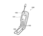
[電子機器]
図8は、本発明に係る電子機器の一例である携帯電話の斜視図である。この図に示す携帯電話1300は、上記各実施形態の液晶装置を小サイズの表示部1301として備え、複数の操作ボタン1302、受話口1303、及び送話口1304を備えて構成されている。
上記各実施形態の液晶装置は、携帯電話に限らず、電子ブック、パーソナルコンピュータ、ディジタルスチルカメラ、液晶テレビ、ビューファインダ型あるいはモニタ直視型のビデオテープレコーダ、カーナビゲーション装置、ページャ、電子手帳、電卓、ワードプロセッサ、ワークステーション、テレビ電話、POS端末、タッチパネルを備えた機器等々の画像表示手段として好適に用いることができ、いずれにおいても信頼性が高く表示品質に優れた電子機器を提供することができる。
[Electronics]
FIG. 8 is a perspective view of a mobile phone which is an example of an electronic apparatus according to the present invention. A
The liquid crystal device of each of the above embodiments is not limited to a mobile phone, but is an electronic book, a personal computer, a digital still camera, a liquid crystal television, a viewfinder type or a monitor direct view type video tape recorder, a car navigation device, a pager, an electronic notebook, a calculator. It can be suitably used as an image display means for a word processor, a workstation, a videophone, a POS terminal, a device equipped with a touch panel, etc., and any of them can provide an electronic device with high reliability and excellent display quality. .
なお、本発明の技術範囲は、上述した各実施形態に限定されるものではなく、本発明の趣旨を逸脱しない範囲において、上述した各実施形態に種々の変更を加えたものを含む。すなわち、各実施形態で挙げた具体的な材料や構成などはほんの一例に過ぎず、適宜変更が可能である。 The technical scope of the present invention is not limited to the above-described embodiments, and includes various modifications made to the above-described embodiments without departing from the spirit of the present invention. That is, the specific materials and configurations described in the embodiments are merely examples, and can be changed as appropriate.
9透明電極 10基板 16有機配向膜 20基板 21透明電極 22有機配向膜 50液晶層 60液晶装置 80撥水層 90撥水層
9
Claims (8)
前記一対の基板の少なくとも一方の基板に形成され前記液晶層に電界を印加する透明導電膜の表面に、撥水層が形成されていることを特徴とする液晶装置。 A liquid crystal device in which a liquid crystal layer is sandwiched between a pair of substrates,
A liquid crystal device, wherein a water repellent layer is formed on a surface of a transparent conductive film which is formed on at least one of the pair of substrates and applies an electric field to the liquid crystal layer.
Priority Applications (1)
| Application Number | Priority Date | Filing Date | Title |
|---|---|---|---|
| JP2004110862A JP4165429B2 (en) | 2004-04-05 | 2004-04-05 | Liquid crystal device, projector and electronic device |
Applications Claiming Priority (1)
| Application Number | Priority Date | Filing Date | Title |
|---|---|---|---|
| JP2004110862A JP4165429B2 (en) | 2004-04-05 | 2004-04-05 | Liquid crystal device, projector and electronic device |
Publications (2)
| Publication Number | Publication Date |
|---|---|
| JP2005292685A true JP2005292685A (en) | 2005-10-20 |
| JP4165429B2 JP4165429B2 (en) | 2008-10-15 |
Family
ID=35325639
Family Applications (1)
| Application Number | Title | Priority Date | Filing Date |
|---|---|---|---|
| JP2004110862A Expired - Fee Related JP4165429B2 (en) | 2004-04-05 | 2004-04-05 | Liquid crystal device, projector and electronic device |
Country Status (1)
| Country | Link |
|---|---|
| JP (1) | JP4165429B2 (en) |
Cited By (5)
| Publication number | Priority date | Publication date | Assignee | Title |
|---|---|---|---|---|
| CN102830567A (en) * | 2012-08-29 | 2012-12-19 | 信利半导体有限公司 | Electronic ink display thin film, electronic ink display panel and manufacturing method of electronic ink display thin film |
| US8809864B2 (en) | 2011-06-27 | 2014-08-19 | Samsung Display Co., Ltd. | Liquid crystal display and method for manufacturing the same |
| US9523879B2 (en) | 2014-03-18 | 2016-12-20 | Samsung Display Co., Ltd. | Liquid crystal display and method for fabricating the same |
| US9880424B2 (en) | 2014-12-19 | 2018-01-30 | Japan Display Inc. | Liquid crystal display panel |
| CN111416964A (en) * | 2020-05-09 | 2020-07-14 | 黄河勘测规划设计研究院有限公司 | Remote image intelligent identification method for hydraulic engineering deformation |
-
2004
- 2004-04-05 JP JP2004110862A patent/JP4165429B2/en not_active Expired - Fee Related
Cited By (8)
| Publication number | Priority date | Publication date | Assignee | Title |
|---|---|---|---|---|
| US8809864B2 (en) | 2011-06-27 | 2014-08-19 | Samsung Display Co., Ltd. | Liquid crystal display and method for manufacturing the same |
| US8912026B2 (en) | 2011-06-27 | 2014-12-16 | Samsung Display Co., Ltd. | Liquid crystal display and method for manufacturing the same |
| CN102830567A (en) * | 2012-08-29 | 2012-12-19 | 信利半导体有限公司 | Electronic ink display thin film, electronic ink display panel and manufacturing method of electronic ink display thin film |
| CN102830567B (en) * | 2012-08-29 | 2014-11-19 | 信利半导体有限公司 | Electronic ink display thin film, electronic ink display panel and manufacturing method of electronic ink display thin film |
| US9523879B2 (en) | 2014-03-18 | 2016-12-20 | Samsung Display Co., Ltd. | Liquid crystal display and method for fabricating the same |
| US9880424B2 (en) | 2014-12-19 | 2018-01-30 | Japan Display Inc. | Liquid crystal display panel |
| CN111416964A (en) * | 2020-05-09 | 2020-07-14 | 黄河勘测规划设计研究院有限公司 | Remote image intelligent identification method for hydraulic engineering deformation |
| CN111416964B (en) * | 2020-05-09 | 2021-08-24 | 黄河勘测规划设计研究院有限公司 | Remote image intelligent identification method for hydraulic engineering deformation |
Also Published As
| Publication number | Publication date |
|---|---|
| JP4165429B2 (en) | 2008-10-15 |
Similar Documents
| Publication | Publication Date | Title |
|---|---|---|
| CN102193262B (en) | Electro-optical device and electronic equipment | |
| US20050200799A1 (en) | Electro-optical device, method of manufacturing the same, and electronic apparatus | |
| US20070188689A1 (en) | Electro-optical device, panel for electro-optical device, method of manufacturing electro-optical device, and electronic apparatus | |
| US20100078666A1 (en) | Electro-optical device, electronic apparatus, and transistor | |
| US6816355B2 (en) | Capacitor, semiconductor device, electro-optic device, method of manufacturing capacitor, method of manufacturing semiconductor device, and electronic apparatus | |
| JP4165429B2 (en) | Liquid crystal device, projector and electronic device | |
| JP2010096966A (en) | Electro-optical apparatus, method for manufacturing same, and electronic device | |
| CN100477237C (en) | Electro-optic device, manufacturing method thereof, electronic device, and capacitor | |
| JP2013041131A (en) | Electro-optical device and electronic apparatus | |
| KR100698000B1 (en) | Substrate for semiconductor device and manufacturing method thereof, electro-optical device substrate, electro-optical device and electronic device | |
| JP2011186285A (en) | Electrooptic device and method for manufacturing the same, and electronic equipment | |
| JP2010008635A (en) | Method of manufacturing substrate for electrooptical device, substrate for electrooptical device, electrooptical device, and electronic equipment | |
| JP2006201236A (en) | Liquid crystal device manufacturing method and liquid crystal device manufacturing apparatus | |
| JP2003167255A (en) | Liquid crystal device, method of manufacturing substrate for liquid crystal device, and electronic apparatus | |
| JP2011221119A (en) | Electro-optic device, electronic equipment, and manufacturing method of electro-optic device | |
| JP4221955B2 (en) | Electro-optical device, electronic device, and active matrix substrate | |
| JP5145944B2 (en) | Electro-optical device and electronic apparatus | |
| JP5343476B2 (en) | Electro-optical device and electronic apparatus | |
| JP4462128B2 (en) | ELECTRO-OPTICAL DEVICE, MANUFACTURING METHOD THEREOF, AND ELECTRONIC DEVICE | |
| JP2011075773A (en) | Electro-optical apparatus and electric apparatus | |
| JP2006195235A (en) | Method for manufacturing liquid crystal device, liquid crystal device, and projection display device | |
| JP2007225663A (en) | Method for manufacturing liquid crystal device, liquid crystal device, and electronic apparatus | |
| JP2007140018A (en) | Liquid crystal device, method for manufacturing liquid crystal device, substrate for liquid crystal device, projector | |
| JP2009186877A (en) | ELECTRO-OPTICAL DEVICE, MANUFACTURING METHOD THEREOF, AND ELECTRONIC DEVICE | |
| JP2011158700A (en) | Electro-optical device and electronic apparatus, and method for manufacturing the electro-optical device |
Legal Events
| Date | Code | Title | Description |
|---|---|---|---|
| A621 | Written request for application examination |
Free format text: JAPANESE INTERMEDIATE CODE: A621 Effective date: 20070307 |
|
| A521 | Written amendment |
Free format text: JAPANESE INTERMEDIATE CODE: A821 Effective date: 20070308 |
|
| A977 | Report on retrieval |
Free format text: JAPANESE INTERMEDIATE CODE: A971007 Effective date: 20080418 |
|
| A131 | Notification of reasons for refusal |
Free format text: JAPANESE INTERMEDIATE CODE: A131 Effective date: 20080425 |
|
| A521 | Written amendment |
Free format text: JAPANESE INTERMEDIATE CODE: A523 Effective date: 20080609 |
|
| TRDD | Decision of grant or rejection written | ||
| A01 | Written decision to grant a patent or to grant a registration (utility model) |
Free format text: JAPANESE INTERMEDIATE CODE: A01 Effective date: 20080708 |
|
| A01 | Written decision to grant a patent or to grant a registration (utility model) |
Free format text: JAPANESE INTERMEDIATE CODE: A01 |
|
| A61 | First payment of annual fees (during grant procedure) |
Free format text: JAPANESE INTERMEDIATE CODE: A61 Effective date: 20080721 |
|
| R150 | Certificate of patent or registration of utility model |
Ref document number: 4165429 Country of ref document: JP Free format text: JAPANESE INTERMEDIATE CODE: R150 Free format text: JAPANESE INTERMEDIATE CODE: R150 |
|
| FPAY | Renewal fee payment (event date is renewal date of database) |
Free format text: PAYMENT UNTIL: 20110808 Year of fee payment: 3 |
|
| FPAY | Renewal fee payment (event date is renewal date of database) |
Free format text: PAYMENT UNTIL: 20120808 Year of fee payment: 4 |
|
| FPAY | Renewal fee payment (event date is renewal date of database) |
Free format text: PAYMENT UNTIL: 20130808 Year of fee payment: 5 |
|
| S531 | Written request for registration of change of domicile |
Free format text: JAPANESE INTERMEDIATE CODE: R313531 |
|
| R350 | Written notification of registration of transfer |
Free format text: JAPANESE INTERMEDIATE CODE: R350 |
|
| R250 | Receipt of annual fees |
Free format text: JAPANESE INTERMEDIATE CODE: R250 |
|
| LAPS | Cancellation because of no payment of annual fees |