JP2005292627A - Optical scanning device - Google Patents
Optical scanning device Download PDFInfo
- Publication number
- JP2005292627A JP2005292627A JP2004109999A JP2004109999A JP2005292627A JP 2005292627 A JP2005292627 A JP 2005292627A JP 2004109999 A JP2004109999 A JP 2004109999A JP 2004109999 A JP2004109999 A JP 2004109999A JP 2005292627 A JP2005292627 A JP 2005292627A
- Authority
- JP
- Japan
- Prior art keywords
- light beam
- position detection
- signal
- optical scanning
- scanning device
- Prior art date
- Legal status (The legal status is an assumption and is not a legal conclusion. Google has not performed a legal analysis and makes no representation as to the accuracy of the status listed.)
- Pending
Links
Images


Landscapes
- Mechanical Optical Scanning Systems (AREA)
- Facsimile Heads (AREA)
- Facsimile Scanning Arrangements (AREA)
- Laser Beam Printer (AREA)
Abstract
【課題】 偏向ミラーによる光ビーム走査位置を精度良く検知する光走査装置を提供する。
【解決手段】 光ビームを発生する光ビーム発生手段と、前記光ビームを入射させ、駆動可能な偏向ミラーにより前記光ビームを偏向・出射させる光ビーム偏向手段と、前記光ビーム偏向手段により偏向走査された前記光ビームが所定の位置を走査通過したとき、前記光ビームを検知し、位置検知信号を出力する位置検知信号生成手段と、前記位置検出信号に応じて、前記偏向ミラーの駆動周期に同期して同期基準信号を発生させる同期基準信号生成手段と、同期基準信号に基づき前記偏向ミラーを駆動する駆動信号を発生するとともに、前記偏向ミラーの駆動制御をする偏向ミラー駆動手段と、同期基準信号に基づき、前記位置検出信号間の時間差を計測する基準クロックを生成する基準クロック生成手段と、前記基準クロックに基づき、前記任意の位置検出信号間の時間差を計測する計測手段とを有する。
【選択図】 図2PROBLEM TO BE SOLVED: To provide an optical scanning device for accurately detecting a light beam scanning position by a deflection mirror.
Light beam generating means for generating a light beam, light beam deflecting means for making the light beam incident, deflecting and emitting the light beam by a driveable deflection mirror, and deflection scanning by the light beam deflecting means. The detected light beam scans a predetermined position, detects the light beam, outputs a position detection signal, and generates a position detection signal, and according to the position detection signal, the driving cycle of the deflection mirror A synchronization reference signal generating means for generating a synchronization reference signal in synchronism; a deflection mirror driving means for generating a drive signal for driving the deflection mirror based on the synchronization reference signal; A reference clock generating means for generating a reference clock for measuring a time difference between the position detection signals based on the signal; Measuring means for measuring a time difference between arbitrary position detection signals.
[Selection] Figure 2
Description
本発明は、偏向ミラーを用いた光走査装置に関する。 The present invention relates to an optical scanning device using a deflection mirror.
近年、光ビームを走査する光走査装置は、光ディスクやレーザプリンタなどでの光ビームを走査する為に用いられている。これらを用いた光走査装置は、シリコンマイクロマシニング技術を利用した微小ミラーを揺動させる構成の物が提案されている。 In recent years, an optical scanning device that scans a light beam is used to scan the light beam in an optical disk, a laser printer, or the like. An optical scanning device using these has been proposed that swings a micromirror using silicon micromachining technology.
このようなマイクロミラーディバイスはその駆動方式から大別して、電磁駆動方式、静電駆動方式が提案されている。特許文献1では磁界発生手段を用いた方法が提案されている。また特許文献2では静電誘導発生手段を用いた方法が提案されている。このような従来の提案では、マイクロミラー可動部の駆動方式として、磁界発生手段を用いた駆動方式或は静電誘導発生手段を用いた駆動方式では駆動電圧を正弦波交流信号として定常的に印加して駆動する方式となっている。
Such micromirror devices are roughly classified into their driving methods, and an electromagnetic driving method and an electrostatic driving method have been proposed.
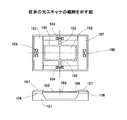
代表的な例として図1に特許文献3で開示された静電引力によってミラーを揺動させる光走査装置を示している。図1において、支持基板101に設けられた凹部にミラー102が配置され、このミラーは一体的に設けられたトーションバー103を介して支持基板101に支持される。ミラー102はトーションバー103の捩じり作用により、その両側がミラーの平面に対して垂直方向に揺動可能としている。
As a typical example, FIG. 1 shows an optical scanning device that swings a mirror by electrostatic attraction disclosed in
トーションバー103は導電性部材で構成され、その両端は支持基板101に設けられたパッド104に電気接続されている。さらに、支持基板101の凹部の両側には絶縁体106を介して固定電極107が支持されている。
The
固定電極107は、ミラー102の両側にあるミラー電極部105との位置関係を、ミラー電極部105の初期位置よりも揺動方向に沿って高い位置に配置する構成となっており、ミラー電極部105の初期位置においてミラー電極部105と固定電極部107とは高低差を持って配置したものとなっている。
The
この装置は、固定電極107のパッド108とトーションバー103が接続されたパッド104との間に高電圧を印加し、固定電極107とミラー102との間に静電力を発生させ、その静電引力によってミラー102の一方の側面を固定電極107側に吸引する。
This apparatus applies a high voltage between the
この吸引動作によってトーションバー103を捩じり変形させながらミラー102をミラーの平面に対して垂直方向に揺動させる。この揺動動作の直後に固定電極107への弾圧印加を解除すると、トーションバー103の捩じり復元力によってミラーは逆方向に揺動される。
By this suction operation, the
この電圧印加と停止を繰り返すことにより、ミラー102を揺動させることが出来、光源からの光をミラー102で反射させることで、光を偏向、走査が可能となる。
上記何れの提案においても、ミラーの揺動角は、ミラー可動部材の固有振動数に共振する共振周波数での周期で揺動せしめて最大角度を得る様に用いる構成としている。ところが、一般に固有振動数に共振させた共振周波数での駆動はQ値が高い位置での使用となるため、駆動信号の電圧変動、或は可動部材の温度による固有振動数変動等により、駆動周波数から外れミラーの揺動角の減少が発生する。 In any of the above proposals, the mirror swing angle is used to obtain the maximum angle by swinging the mirror at a resonance frequency that resonates with the natural frequency of the mirror movable member. However, since driving at a resonance frequency resonated at the natural frequency is generally used at a position where the Q value is high, the drive frequency may vary depending on the voltage fluctuation of the drive signal or the natural frequency fluctuation due to the temperature of the movable member. This causes a decrease in the swing angle of the mirror.
ミラーの揺動角を一定にするため、ミラーの揺動位置を検知してミラー駆動のタイミングを調整する必要がある。また、複数のミラーを用いたシステムで複数のミラーを同一の共振周波数で駆動する場合、複数ミラーの揺動位置を検知し、お互いに同期して駆動する事が必要である。 In order to make the mirror swing angle constant, it is necessary to detect the mirror swing position and adjust the mirror drive timing. Further, when a plurality of mirrors are driven at the same resonance frequency in a system using a plurality of mirrors, it is necessary to detect the swing positions of the plurality of mirrors and drive them in synchronization with each other.
上記の様、何れの場合でもミラーの揺動に同期して駆動パルスを印加するためには、ミラーの揺動位置を測定する事が必要であり、特許文献3では駆動電極の容量変化を検知しミラーの位置を検知している。また、特許文献1ではミラーの揺動位置検知にコイルを用いている。また、特許文献5では光ビームを検知してミラーの角度を検出している。
As described above, in any case, in order to apply the drive pulse in synchronization with the mirror swing, it is necessary to measure the mirror swing position. In
また、従来はQ値が高く、光ビームの偏向角を正確に検知する為、高精度のセンサを多数設置する必要があったり、検知回路が複雑になり製造コストも増大する問題があった。 Conventionally, since the Q value is high and the deflection angle of the light beam is accurately detected, it is necessary to install a large number of high-precision sensors, and the detection circuit becomes complicated and the manufacturing cost increases.
本発明はこのような問題点に鑑み、偏向ミラーによる光ビーム走査位置を精度良く検知する光走査装置を提供することを目的とする。 SUMMARY OF THE INVENTION The present invention has been made in view of such problems, and an object of the present invention is to provide an optical scanning device that accurately detects a light beam scanning position by a deflection mirror.
上記課題を解決するために、本発明は、光ビームを発生する光ビーム発生手段と、前記光ビームを入射させ、駆動可能な偏向ミラーにより前記光ビームを偏向・出射させる光ビーム偏向手段と、前記光ビーム偏向手段により偏向走査された前記光ビームが所定の位置を走査通過したとき、前記光ビームを検知し、位置検知信号を出力する位置検知信号生成手段と、前記位置検出信号に応じて、前記偏向ミラーの駆動周期に同期して同期基準信号を発生させる同期基準信号生成手段と、同期基準信号に基づき前記偏向ミラーを駆動する駆動信号を発生するとともに、前記偏向ミラーの駆動制御をする偏向ミラー駆動手段と、同期基準信号に基づき、前記位置検出信号間の時間差を計測する基準クロックを生成する基準クロック生成手段と、前記基準クロックに基づき、前記任意の位置検出信号間の時間差を計測する計測手段とを有することを特徴とする。 In order to solve the above problems, the present invention comprises a light beam generating means for generating a light beam, a light beam deflecting means for causing the light beam to enter, and deflecting and emitting the light beam by a driveable deflection mirror, Position detection signal generating means for detecting the light beam and outputting a position detection signal when the light beam deflected and scanned by the light beam deflecting means passes through a predetermined position; and according to the position detection signal A synchronization reference signal generating means for generating a synchronization reference signal in synchronization with a drive cycle of the deflection mirror; a drive signal for driving the deflection mirror based on the synchronization reference signal; and a drive control of the deflection mirror Deflection mirror driving means; reference clock generating means for generating a reference clock for measuring a time difference between the position detection signals based on a synchronization reference signal; and Based on the reference clock, and having a measuring means for measuring a time difference between said arbitrary position detection signal.
また、上記課題を解決するために、本発明は、前記位置検知信号生成手段は、前記光ビームが所定の位置を走査通過した時に、前記光ビームを検知して位置検知信号を発生する光センサであることを特徴とする。 In order to solve the above-mentioned problem, the present invention provides an optical sensor, wherein the position detection signal generation means detects the light beam and generates a position detection signal when the light beam scans a predetermined position. It is characterized by being.
また、上記課題を解決するために、本発明は、前記光センサは、偏向ミラーに拠る光ビームの走査開始位置近傍と走査終了位置近傍の両方に設けられることを特徴とする。 In order to solve the above problem, the present invention is characterized in that the optical sensor is provided near both the scanning start position and the scanning end position of the light beam due to the deflection mirror.
また、上記課題を解決するために、本発明は、前記基準クロックは、前記同期基準信号に同期して毎回新規に生成されることを特徴とする。 In order to solve the above problem, the present invention is characterized in that the reference clock is newly generated every time in synchronization with the synchronization reference signal.
また、上記課題を解決するために、本発明は、前記偏向ミラー駆動手段は、前記各光センサが発生した位置検出信号に基づき計測された値を、予め設定された基準値にするように、前記駆動信号を発生し、前記偏向ミラーを制御することを特徴とする。 In order to solve the above-described problem, the present invention provides the deflecting mirror driving means, wherein the value measured based on the position detection signal generated by each optical sensor is set to a preset reference value. The drive signal is generated and the deflection mirror is controlled.
また、上記課題を解決するために、本発明は、前記偏向ミラー駆動手段は、前記各光センサが発生した位置検出信号に基づき計測された値を、予め設定された基準値にするように、前記駆動信号への電圧を制御することを特徴とする。 In order to solve the above-described problem, the present invention provides the deflecting mirror driving means, wherein the value measured based on the position detection signal generated by each optical sensor is set to a preset reference value. The voltage to the drive signal is controlled.
また、上記課題を解決するために、本発明は、前記計測された値は、前記光センサが発生した信号である第1の位置検出信号と第2の位置信号とが発生した間隔から定まる値であることを特徴とする。 In order to solve the above problem, the present invention provides that the measured value is a value determined from an interval at which a first position detection signal and a second position signal, which are signals generated by the optical sensor, are generated. It is characterized by being.
また、上記課題を解決するために、本発明は、前記第1、第2の位置検出信号は、同一の光センサが発生した信号であることを特徴とする。 In order to solve the above problem, the present invention is characterized in that the first and second position detection signals are signals generated by the same optical sensor.
また、上記課題を解決するために、本発明は、前記第1、第2の位置検出信号は、異なる光センサが発生した信号であることを特徴とする。 In order to solve the above problems, the present invention is characterized in that the first and second position detection signals are signals generated by different optical sensors.
また、上記課題を解決するために、本発明は、前記光センサが前記第1、第2の位置検出信号を発生した際に検知したそれぞれの光ビームの走査した方向は、同一方向であることを特徴とする。 In order to solve the above problems, the present invention is directed to the same scanning direction of each light beam detected when the optical sensor generates the first and second position detection signals. It is characterized by.
また、上記課題を解決するために、本発明は、前記光センサが前記第1、第2の位置検出信号を発生した際に検知したそれぞれの光ビームの走査した方向は、異なる方向であることを特徴とする。 In order to solve the above-described problem, the present invention is directed to a scanning direction of each light beam detected when the optical sensor generates the first and second position detection signals. It is characterized by.
また、上記課題を解決するために、本発明は、前記偏向ミラーを配設した可動部材と、前記可動部材を揺動可能に支持する支持部材とを有し、前記偏向ミラー駆動手段は、前記可動部材の持つ固有振動数に共振する共振周波数を除いた周波数領域で前記可動部材を揺動することを特徴とする。 In order to solve the above-mentioned problem, the present invention includes a movable member provided with the deflection mirror, and a support member that supports the movable member in a swingable manner. The movable member is oscillated in a frequency range excluding a resonance frequency that resonates with a natural frequency of the movable member.
本発明は以上説明したように、偏向ミラーによる光ビーム走査位置を精度良く検知する光走査装置を提供することができる。 As described above, the present invention can provide an optical scanning device that accurately detects a light beam scanning position by a deflection mirror.
以下、図面を参照し、本発明の実施形態について説明する。 Hereinafter, embodiments of the present invention will be described with reference to the drawings.
図2は、本実施の形態に係る光走査装置を用いた書き込み装置の概略を示す。この図2においては、ビーム発生手段をレーザー光とした例について述べる。 FIG. 2 schematically shows a writing device using the optical scanning device according to the present embodiment. In FIG. 2, an example in which the beam generating means is a laser beam will be described.
図2には、レーザー光源200と、集光レンズ201と、アパーチャ202と、シリンダーレンズA203と、偏向ミラー40と、fθレンズ207,208と、光路変更ミラー209と、シリンダーレンズB210と、感光体211と、同期検知ミラー213と、光センサ215a、215bとが示されている。これら215a、215bで発生する位置検知信号は、第1、2の位置検出信号に対応する。
FIG. 2 shows a
レーザー光源200から出射された光ビームは集光レンズ201により平行光にされ、ドットの大きさに応じたスリット部を持つアパーチャ202により必要なビーム径のみ取り出され、シリンダーレンズA203により適正なビーム径に形成され、光ビーム偏向手段である偏向ミラー40により感光体の長軸方向である主走査方向に走査される。
The light beam emitted from the
光路上には等角走査を等速走査への変換用fθレンズ207,208、光路偏向ミラー209、感光体回転方向への集光を行なうシリンダーレンズB210が配され、感光体211面上に微小レーザービームスポットが結像される。
同期検知ミラー213に拠って折り返されたビームは光センサ215に照射され同期信号が生成される。この様に光センサを設ける事により光ビームの位置を検知する事が出来る。 The beam folded back by the synchronization detection mirror 213 is irradiated to the optical sensor 215 to generate a synchronization signal. Thus, the position of the light beam can be detected by providing the optical sensor.
図2において、光センサ215a、215bは其々光ビームの光走査開始位置、或は光走査終了位置近傍に配置されている。この様に光ビームの走査領域両端に光センサを配置する事により、光ビームの走査有効領域を走査する走査時間を監視する事が出来る。
In FIG. 2, the
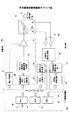
次に、図3を用いて、光走査装置のブロック図について説明する。図3には、RAM33と、ROM32と、MPU31と、クロック30と、アドレス/データバス34と、駆動信号発生タイミング制御部36と、プログラマブル発振器/駆動信号発生器39と、電圧可変部47と、ドライバーアンプ部41と、光ビーム発生部51と、偏向ミラー40と、光センサ215a、215bと、センサアンプ部42と、位置信号生成部38と、基準クロック生成部48と、時間計測部49と、同期信号生成部37と、時間差演算回路46とが示されている。
Next, a block diagram of the optical scanning device will be described with reference to FIG. 3 includes a
このうち、光ビーム発生部51は光ビーム発生手段に対応する。偏向ミラー40は、光ビーム偏向手段に対応する。位置検知信号生成部38は、位置検知信号生成手段に対応する。同期信号生成部37は、同期信号生成手段に対応する。基準クロック生成部48は、基準クロック生成手段に対応する。時間計測部49は、計測手段に対応する。
Among these, the light beam generator 51 corresponds to a light beam generator. The
電圧可変部47、駆動信号発生タイミング制御部36、プログラマブル発信器/駆動信号生成部39、ドライバーアンプ部41より構成される駆動部500は光走査装置43の偏向ミラー40を揺動可能とする。この駆動部500は、偏向ミラー駆動手段に対応する。
A
センサアンプ部42、位置検知信号生成部38、同期基準信号生成部37、基準クロック生成部48より構成される検出部520は、光走査装置の信号検知部から取り出された信号を検知及び格納する。MPU31、ROM32、RAM33、アドレス/データバス34は、データ信号処理部510を構成する。
A detection unit 520 including a
駆動部500はデータ信号処理部510からの制御指示に従い、電圧可変部47では電極に印加する電圧を設定し、駆動信号発生タイミング制御部36には電極に印可する信号の駆動周波数に関するデータが格納され、プログラマブル発信器/駆動信号生成部39では駆動信号発生タイミング制御部36で格納されたデータに対応した駆動周波数を生成する。
In accordance with a control instruction from the data
プログラマブル発信器/駆動信号生成部39で生成された信号はドライバーアンプ部41に接続されている。ドライバーアンプ部41では信号印加電圧が電圧可変部47により任意に可変可能となっている。
The signal generated by the programmable transmitter / driving
ドライバーアンプ部41の出力は光走査装置に配設された端子に接続され各電極に信号を与える。検知部は光走査装置の信号検知部から取り出された信号をセンサアンプ部42で増幅し、位置検知信号生成部38で位置検知信号を生成し、位置検知信号から同期基準信号生成部37にて同期基準信号を生成する。
The output of the
また基準クロック生成部48にて同期基準信号に同期したクロックを生成し、各同期基準信号間の時間を計測するのに利用する。データ信号処理部510と駆動部500及び検出部520間はアドレス/データバス34を経由してデータ或は指令の授受を行い、データ信号処理部510での所定の制御処理手順に従った動作を行う。
The reference
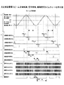
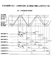
以上説明した光走査装置における動作のタイムチャートを、図4を用いて説明する。図4には、グラフA〜Eが示されている。グラフAは、光ビームの走査軌跡を示している。グラフBは、光走査開始位置、または光走査終了位置の近傍に配置された光センサより検出された各々の位置信号を示している。グラフCは、同期基準信号を示している。グラフDは、生成される基準クロックを示している。グラフEは、駆動信号を示している。 A time chart of the operation of the optical scanning apparatus described above will be described with reference to FIG. In FIG. 4, graphs A to E are shown. Graph A shows the scanning trajectory of the light beam. Graph B shows each position signal detected by the optical sensor disposed in the vicinity of the optical scanning start position or the optical scanning end position. Graph C shows the synchronization reference signal. Graph D shows the generated reference clock. Graph E shows the drive signal.
任意の周波数の駆動信号を印加すると偏向ミラーは往復運動を行い、グラフAに示される単振動波形の光ビーム軌跡が生じる。光センサ215a、215bは、其々光ビームの光走査開始位置或は光走査終了位置近傍に配置されており、各々で検出された位置信号が以下のように図3のグラフBに示されている。
PS(a,n),PS(b,n),PS(c,n),PS(d,n),PS(a,n+1),PS(b,n+1),PS(c,n+1),PS(d,n+1)...
(n≧1の整数)
これらの位置信号に同期して、グラフCに示される以下の同期基準信号が生成される。
P(a,n),P(b,n),P(c,n),P(d,n),P(a,n+1),P(b,n+1),(c,n+1),P(d,n+1),
これらの同期基準信号を基準にして、光走査装置の駆動タイミング等の制御は行われる。また、上記P(a,n),P(b,n),P(c,n),P(d,n)等の同期信号に同期して、グラフDに示される基準クロックが生成される。
When a drive signal having an arbitrary frequency is applied, the deflecting mirror reciprocates, and a light beam locus having a simple vibration waveform shown in graph A is generated. The
PS (a, n), PS (b, n), PS (c, n), PS (d, n), PS (a, n + 1), PS (b, n + 1), PS (c, n + 1), PS (d, n + 1) ...
(integer with n ≧ 1)
In synchronization with these position signals, the following synchronization reference signals shown in graph C are generated.
P (a, n), P (b, n), P (c, n), P (d, n), P (a, n + 1), P (b, n + 1), (c, n +1), P (d, n + 1),
Control of the driving timing of the optical scanning device and the like is performed based on these synchronization reference signals. Further, the reference clock shown in the graph D is generated in synchronization with the synchronization signals such as P (a, n), P (b, n), P (c, n), and P (d, n). .
基準クロックは、同期基準信号に同期して毎回新規に生成され、この基準クロックにより、上記位置信号の任意の信号間の時間が計測される。 The reference clock is newly generated every time in synchronization with the synchronization reference signal, and the time between arbitrary signals of the position signals is measured by this reference clock.
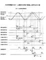
次に、図5を用いて、標準正弦波振動軌跡波形に対し、振幅が同じで正弦波振動周期が変動した場合の事例について説明する。この図5に示される軌跡は、標準波形より駆動波形の周期が長くなった場合である。この場合、標準波形の軌跡で得られる信号の各タイミングを計測する事により、変動分を補正し標準波形と同一にするように制御する。 Next, a case where the amplitude is the same and the sine wave vibration cycle varies with respect to the standard sine wave vibration locus waveform will be described with reference to FIG. The locus shown in FIG. 5 is a case where the period of the drive waveform is longer than the standard waveform. In this case, by measuring each timing of the signal obtained from the locus of the standard waveform, the fluctuation is corrected and controlled to be the same as the standard waveform.
図5において、信号に注目してみると、標準信号のS(a,n)とS(a,n+1)の時間T(a,1)と、駆動波形から得た信号PS(a,n)とPS(a,n+1)の時間T'(a,1)を比較するとT'(a,1)>T(a,1)となっている。 In FIG. 5, when attention is paid to the signal, the time T (a, 1) of S (a, n) and S (a, n + 1) of the standard signal and the signal PS (a, Comparing the time T ′ (a, 1) of n) and PS (a, n + 1), T ′ (a, 1)> T (a, 1).
また、標準信号のS(b,n)とS(b,n+1)の時間T(b,1)と、駆動波形から得た信号PS(b,n)とPS(b,n+1)の時間T'(b,1)を比較するとT'(b,1)>T(b,1)であり、これらの事より標準波形より駆動波形の周期が長いと推測される。 Also, the time T (b, 1) of the standard signal S (b, n) and S (b, n + 1), and the signal PS (b, n) and PS (b, n + 1) obtained from the drive waveform ) At time T ′ (b, 1), T ′ (b, 1)> T (b, 1). From these facts, it is estimated that the period of the drive waveform is longer than that of the standard waveform.
そこで、周期を小さくするために、駆動信号発生タイミング制御部36(図3参照)にて駆動信号印加タイミングを可変しドライバー部41に供給する。このとき周波数の変化量は基準クロックの1クロック単位における周波数変化量を予め変化量テーブルとして記憶しておき、この変化量テーブルを参照して決定する。
Therefore, in order to reduce the cycle, the drive signal generation timing control unit 36 (see FIG. 3) varies the drive signal application timing and supplies it to the
図5の場合は駆動周波数を大きくして実現する事が出来る。この図5における補正駆動信号の印加について説明する。 In the case of FIG. 5, it can be realized by increasing the driving frequency. Application of the correction drive signal in FIG. 5 will be described.
位置検知信号PS(a,n+1)検知の時点での演算の結果、T'(a,1)>T(a,1)となり駆動周期が変動し長くなっている事を検知すると、駆動信号の印加タイミングを調整する必要がある。この場合、PS(a,n+1)時点から次の駆動信号は検知信号PS(b,n+1)の前後で駆動信号HD1を印加する。このときPS(a,n+1)を基準にして、タイミングTnを調整する事により、偏向ミラーの揺動の速度を速める様駆動信号HD1を印加する。 When the position detection signal PS (a, n + 1) is detected at the time of detection, T '(a, 1)> T (a, 1) and the drive cycle is detected to change and become longer. It is necessary to adjust the signal application timing. In this case, the drive signal HD1 is applied before and after the detection signal PS (b, n + 1) as the next drive signal from the time point PS (a, n + 1). At this time, the drive signal HD1 is applied so as to increase the swinging speed of the deflection mirror by adjusting the timing Tn with reference to PS (a, n + 1).
また駆動信号HD1印加時間Tlの時間も調整する。同様に検知信号PS(c,n+1)検知時点でT'(c,1)>T(c,1)を演算結果として得た場合、検知信号PS(c,n+1)を基準にして駆動信号HD2印加する、その際タイミングTn2、信号印加時間Tl2を速度が速まるよう調整する。 The drive signal HD1 application time Tl is also adjusted. Similarly, when T '(c, 1)> T (c, 1) is obtained as the calculation result at the time of detection of the detection signal PS (c, n + 1), the detection signal PS (c, n + 1) is used as a reference. When the drive signal HD2 is applied, the timing Tn2 and the signal application time Tl2 are adjusted so as to increase the speed.
タイミングTn,Tn2,印加時間Tl,Tl2の値は基準クロックの1クロック単位における値として、予め変化量テーブルとして記憶しておき、この変化量テーブルを参照して決定する。 The values of the timings Tn, Tn2, and the application times Tl, Tl2 are stored in advance as a change amount table as values in one clock unit of the reference clock, and are determined with reference to the change amount table.
この様に光ビームの走査位置検知信号を検知する事により、偏向ミラーの揺動駆動を制御することが出来る。 By detecting the scanning position detection signal of the light beam in this way, the swing drive of the deflection mirror can be controlled.
次に、偏向ミラー駆動制御について述べる。図6は標準正弦波振動軌跡波形に対して、正弦波振動周波数が同じで振幅が変動した時の事例であり、標準波形より振幅が大きくなった場合を示している。 Next, deflection mirror drive control will be described. FIG. 6 shows an example when the amplitude varies with the same sine wave vibration frequency with respect to the standard sine wave vibration trajectory waveform, and shows a case where the amplitude is larger than the standard waveform.
ここでの制御は、標準波形の軌跡で得られる信号の各タイミングを計測する事により、変動分を補正し標準波形と同一にする制御である。図6において、信号に注目して見ると、標準信号のS(a,n)とS(b,n)の時間Tabと、駆動波形から得た信号PS(a,n)とPS(b,n)の時間T'abを比較するとT'ab>Tabとなっている。 The control here is a control for correcting the variation and making it the same as the standard waveform by measuring each timing of the signal obtained from the locus of the standard waveform. In FIG. 6, when attention is paid to the signal, the time Tab of the standard signal S (a, n) and S (b, n) and the signals PS (a, n) and PS (b, Comparing the time T′ab in n), T′ab> Tab.
また、標準信号のS(c,n)とS(d,n)の時間Tcdと、駆動波形から得た信号PS(c,n)とPS(d,n)の時間T'cdを比較するとT'cd>Tcdである。この事より標準波形より駆動波形の振幅が大きいと推測される。そこで、振幅を小さくするために電圧可変部47(図3参照)にて印加電圧を可変しドライバーアンプ部41に供給する。
When comparing the time Tcd of the standard signal S (c, n) and S (d, n) with the time T'cd of the signal PS (c, n) and PS (d, n) obtained from the drive waveform T′cd> Tcd. From this, it is estimated that the amplitude of the drive waveform is larger than that of the standard waveform. Therefore, in order to reduce the amplitude, the applied voltage is varied by the voltage variable section 47 (see FIG. 3) and supplied to the
このとき電圧の変化量は基準クロックの1クロック単位における電位変化量を予め変化量テーブルとして記憶しておき、この変化量テーブルを参照して決定する。図6の場合は印加電圧を小さくして実現する事が出来る。 At this time, the amount of change in voltage is determined by previously storing the amount of change in potential in one clock unit of the reference clock as a change amount table and referring to this change amount table. The case of FIG. 6 can be realized by reducing the applied voltage.
さらに、図7を用いて偏向ミラー駆動制御について述べる。図7は標準正弦波振動軌跡波形に対して、振幅及び周期が変動した時の事例であり、標準波形より駆動波形の周期が長く、振幅が大きくなった場合を示している。 Further, deflection mirror drive control will be described with reference to FIG. FIG. 7 shows an example in which the amplitude and period fluctuate with respect to the standard sine wave vibration trajectory waveform, and shows a case where the period of the drive waveform is longer than the standard waveform and the amplitude is increased.
この場合、標準波形の軌跡で得られる前記信号の各タイミングを計測する事に拠り変動分を補正し標準波形と同一にするように制御する。図7において、信号に注目して、標準信号のS(a,n)とS(a,n+1)の時間T(a,1)と、駆動波形から得た信号PS(a,n)とPS(a,n+1)の時間T'(a,1)を比較するとT'(a,1)>T(a,1)となっている。また、標準信号のS(b,n)とS(b,n+1)の時間T(b,1)と、駆動波形から得た信号PS(b,n)とPS(b,n+1)の時間T'(b,1)を比較するとT'(b,1)>T(b,1)である。 In this case, control is performed so that the variation is corrected to be the same as the standard waveform by measuring each timing of the signal obtained from the locus of the standard waveform. In FIG. 7, paying attention to the signal, time T (a, 1) of S (a, n) and S (a, n + 1) of the standard signal and signal PS (a, n) obtained from the drive waveform And PS (a, n + 1) time T ′ (a, 1) is compared, T ′ (a, 1)> T (a, 1). Also, the time T (b, 1) of the standard signal S (b, n) and S (b, n + 1), and the signal PS (b, n) and PS (b, n + 1) obtained from the drive waveform ) T ′ (b, 1)> T (b, 1).
この事より標準波形より駆動波形の周期が長いと推測される。そこで、周期を小さくするために駆動信号発生タイミング制御部36(図3参照)にて駆動信号印加タイミングを可変しドライバーアンプ部41に供給する。
From this, it is estimated that the period of the drive waveform is longer than that of the standard waveform. Therefore, in order to reduce the period, the drive signal application timing control unit 36 (see FIG. 3) varies the drive signal application timing and supplies it to the
このとき周波数の変化量は基準クロックの1クロック単位における周波数変化量を予め変化量テーブルとして記憶しておき、この変化量テーブルを参照して決定する。 At this time, the amount of change in frequency is determined by previously storing the amount of change in frequency in units of one clock of the reference clock as a change amount table.
次に、標準信号のS(a,n)とS(b,n)の時間Tabと、駆動波形から得た信号PS(a,n)とPS(b,n)の時間T'abを比較するとT'ab>Tabとなる。また、標準信号のS(c,n)とS(d,n)の時間Tcdと、駆動波形から得た信号PS(c,n)とPS(d,n)の時間T'cdを比較するとT'cd>Tcdである。 Next, compare the time Tab of the standard signal S (a, n) and S (b, n) with the time T'ab of the signal PS (a, n) and PS (b, n) obtained from the drive waveform Then T'ab> Tab. When comparing the time Tcd of the standard signal S (c, n) and S (d, n) with the time T'cd of the signal PS (c, n) and PS (d, n) obtained from the drive waveform T′cd> Tcd.
この事より標準波形より駆動波形の振幅が大きいと推測される。そこで、振幅を小さくするために電圧可変部47(図3参照)にて印加電圧を可変しドライバー41部に供給する。
From this, it is estimated that the amplitude of the drive waveform is larger than that of the standard waveform. Therefore, in order to reduce the amplitude, the applied voltage is varied by the voltage varying unit 47 (see FIG. 3) and supplied to the
このときの電圧の変化量は、基準クロックの1クロック単位における電位変化量を予め記憶しておいた変化量テーブルを参照して決定する。図7の場合は印加電圧を小さくして実現する事が出来る。 The voltage change amount at this time is determined with reference to a change amount table in which the potential change amount in one clock unit of the reference clock is stored in advance. In the case of FIG. 7, it can be realized by reducing the applied voltage.
この様に駆動波形が振幅及び周期が同時に変動した場合でも、光ビーム走査位置を検知する事に拠り振幅の補正、周期の補正をする互いに組合せて実施する事により簡易に標準単振動波形と同一にする事が出来る。 In this way, even when the drive waveform varies in amplitude and period at the same time, it can easily be the same as the standard single vibration waveform by performing a combination of amplitude correction and period correction by detecting the light beam scanning position. Can be made.
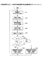
次に、図8のフローチャートを用いて、制御アルゴリズムについて説明する。ステップS101では、駆動信号PS(a,n)とPS(b,n)の検知が行われる。次のステップS102では、T’abを求める演算が行われる。次のステップS103では、標準信号S(a,b)、S(b,n)が参照される。 Next, a control algorithm will be described using the flowchart of FIG. In step S101, the drive signals PS (a, n) and PS (b, n) are detected. In the next step S102, an operation for obtaining T'ab is performed. In the next step S103, the standard signals S (a, b) and S (b, n) are referred to.
次のステップS104では、T’abを求める演算が行われる。求まったTabとT’abとが、ステップS105で比較される。比較の結果、ステップS106で、TabとT’abとが等しいと判断された場合、処理は終了する。 In the next step S104, an operation for obtaining T'ab is performed. The obtained Tab and T′ab are compared in step S105. As a result of the comparison, if it is determined in step S106 that Tab and T′ab are equal, the process ends.
TabとT’abとが等しくない場合、ステップS107で、TabとT’abの大小関係が判断され、Tabの方が大きい場合、ステップS108で、駆動信号印加電圧量が演算され、電位を低くして印加される。Tabの方が小さい場合、ステップS109で、駆動信号印加電圧量が演算され、電位を高くして印加される。 If Tab and T′ab are not equal, the magnitude relationship between Tab and T′ab is determined in step S107. If Tab is larger, the drive signal applied voltage amount is calculated in step S108 to reduce the potential. Applied. If Tab is smaller, in step S109, the drive signal application voltage amount is calculated and applied with a higher potential.
次に、図9のフローチャートを用いて、制御アルゴリズムについて説明する。ステップS201では、駆動信号PS(a,n)とPS(a,n+1)の検知が行われる。次のステップS202では、T’(a,1)を求める演算が行われる。次のステップS203では、標準信号S(a,n)、S(a,n+1)が参照される。 Next, a control algorithm will be described using the flowchart of FIG. In step S201, the drive signals PS (a, n) and PS (a, n + 1) are detected. In the next step S202, an operation for obtaining T '(a, 1) is performed. In the next step S203, the standard signals S (a, n) and S (a, n + 1) are referred to.
次のステップS204では、T(a,1)を求める演算が行われる。求まったT(a,1)とT’(a,1)とが、ステップS205で比較される。比較の結果、ステップS206で、T(a,1)とT’(a,1)とが等しいと判断された場合、処理は終了する。 In the next step S204, an operation for obtaining T (a, 1) is performed. The obtained T (a, 1) and T ′ (a, 1) are compared in step S205. As a result of the comparison, if it is determined in step S206 that T (a, 1) and T ′ (a, 1) are equal, the process ends.
T(a,1)とT’(a,1)とが等しくない場合、ステップS207で、T(a,1)とT’(a,1)の大小関係が判断され、T’(a,1)の方が大きい場合、ステップS208で、駆動信号印加周波数が演算され、周波数を大きくして印加される。T(a,1)の方が小さい場合、ステップS209で、駆動信号印加周波数が演算され、周波数を小さくして印加される。 If T (a, 1) and T ′ (a, 1) are not equal, in step S207, the magnitude relationship between T (a, 1) and T ′ (a, 1) is determined, and T ′ (a, 1) If 1) is larger, in step S208, the drive signal application frequency is calculated and applied with a higher frequency. If T (a, 1) is smaller, in step S209, the drive signal application frequency is calculated and applied with a reduced frequency.
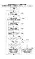
次に、図10、図11のフローチャートを用いて、制御アルゴリズムについて説明する。このフローチャートは、図8、図9のフローチャートを併せたものである。 Next, the control algorithm will be described with reference to the flowcharts of FIGS. This flowchart is a combination of the flowcharts of FIGS.
ステップS301では、駆動信号PS(a,n)とPS(a,n+1)の検知が行われる。次のステップS302では、T’(a,1)を求める演算が行われる。次のステップS303では、標準信号S(a,n)、S(a,n+1)が参照される。 In step S301, the drive signals PS (a, n) and PS (a, n + 1) are detected. In the next step S302, an operation for obtaining T '(a, 1) is performed. In the next step S303, the standard signals S (a, n) and S (a, n + 1) are referred to.
次のステップS304では、T(a,1)を求める演算が行われる。求まったT(a,1)とT’(a,1)とが、ステップS305で比較される。比較の結果、ステップS306で、T(a,1)とT’(a,1)とが等しいと判断された場合、ステップS310へ処理は進む。 In the next step S304, an operation for obtaining T (a, 1) is performed. The obtained T (a, 1) and T ′ (a, 1) are compared in step S305. As a result of the comparison, if it is determined in step S306 that T (a, 1) and T ′ (a, 1) are equal, the process proceeds to step S310.
T(a,1)とT’(a,1)とが等しくない場合、ステップS307で、T(a,1)とT’(a,1)の大小関係が判断され、T’(a,1)の方が大きい場合、ステップS308で、駆動信号印加周波数が演算され、周波数を大きくして印加される。T(a,1)の方が小さい場合、ステップS309で、駆動信号印加周波数が演算され、周波数を小さくして印加される。 If T (a, 1) and T ′ (a, 1) are not equal, in step S307, the magnitude relationship between T (a, 1) and T ′ (a, 1) is determined, and T ′ (a, 1) If 1) is larger, in step S308, the drive signal application frequency is calculated and applied with a larger frequency. If T (a, 1) is smaller, in step S309, the drive signal application frequency is calculated and applied with a reduced frequency.
ステップS310からは図11のフローチャートである。ステップS311では、駆動信号PS(a,n)とPS(b,n)の検知が行われる。次のステップS312では、T’abを求める演算が行われる。次のステップS313では、標準信号S(a,b)、S(b,n)が参照される。 FIG. 11 is a flowchart from step S310. In step S311, the drive signals PS (a, n) and PS (b, n) are detected. In the next step S312, an operation for obtaining T'ab is performed. In the next step S313, the standard signals S (a, b) and S (b, n) are referred to.
次のステップS314では、T’abを求める演算が行われる。求まったTabとT’abとが、ステップS315で比較される。比較の結果、ステップS316で、TabとT’abとが等しいと判断された場合、処理は終了する。 In the next step S314, an operation for obtaining T'ab is performed. The obtained Tab and T′ab are compared in step S315. As a result of the comparison, if it is determined in step S316 that Tab and T′ab are equal, the process ends.
TabとT’abとが等しくない場合、ステップS317で、TabとT’abの大小関係が判断され、Tabの方が大きい場合、ステップS318で、駆動信号印加電圧量が演算され、電位を低くして印加される。Tabの方が小さい場合、ステップS319で、駆動信号印加電圧量が演算され、電位を高くして印加される。 If Tab and T′ab are not equal, the magnitude relationship between Tab and T′ab is determined in step S317. If Tab is greater, the drive signal applied voltage amount is calculated in step S318 to reduce the potential. Applied. If Tab is smaller, in step S319, the drive signal application voltage amount is calculated and applied with a higher potential.
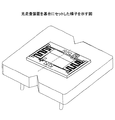
以上が処理内容の説明である。以下、実装について説明する。まず、図10を用いて偏向ミラーについて説明する。偏向ミラーはシリコンマイクロマシニング技術を用いて形成されている。 The above is the description of the processing contents. Hereinafter, the implementation will be described. First, the deflection mirror will be described with reference to FIG. The deflection mirror is formed using silicon micromachining technology.
この偏向ミラーは、シリコン基板1と、支持部材2と、固定電極3と、可動部材配設電極4と、ミラー部9と、可動部材10とで構成される。
The deflecting mirror includes a
シリコン基板1は、矩形の単層厚板で形成される。可動部材10は、可動部材配設電極4とミラー部9が形成されている。可動部材配設電極4に対向して固定電極3と可動部材10に一体的に両側に突出形成された支持部材2は、両端でシリコン基板に固定されている。これにより、前記可動部材10は支持部材2の捩じりにより、ミラー部9の平面方向と垂直な方向に揺動可能となる。
The
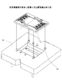
この偏向ミラーを基台に設置する構成について説明する。図13には、偏向ミラーと、基台20とが示されている。基台20には偏向ミラーの図示されていないパッドに接続される接触子23が配置されている。この接触子23を用いて偏向ミラーを基台20に設置した様子を示すのが図14である。
A configuration in which the deflection mirror is installed on the base will be described. FIG. 13 shows the deflection mirror and the
このように、偏向ミラーを配設した可動部材と、前記可動部材を揺動可能に支持する支持部材とを有し、可動部材を揺動可能とする光走査装置において、通常駆動周波数は、可動部材の持つ固有振動数に共振する共振周波数とする事が多い。 As described above, in the optical scanning device having the movable member provided with the deflection mirror and the support member that supports the movable member so as to be swingable, the normal drive frequency is movable. In many cases, the resonance frequency resonates with the natural frequency of the member.
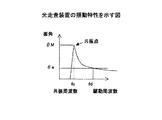
これは、共振周波数点では可動部材の揺動角が最大になる為である。図15は、偏向ミラーの揺動特性図である。この図15の揺動特性図において、可動部材の持つ固有振動数に共振する共振周波数領域は狭く、Q値が高い駆動物体となっている。従来はQ値が高い為光ビームの偏向角を正確に検知する為、高精度のセンサを多数設置する必要があったり、検知回路が複雑になり製造コストも増大する問題があった。 This is because the swing angle of the movable member is maximized at the resonance frequency point. FIG. 15 is a swing characteristic diagram of the deflection mirror. In the oscillation characteristic diagram of FIG. 15, the resonance frequency region resonating with the natural frequency of the movable member is narrow, and the driving object has a high Q value. Conventionally, since the Q value is high, in order to accurately detect the deflection angle of the light beam, it is necessary to install a large number of high-precision sensors, and the detection circuit becomes complicated and the manufacturing cost increases.
本実施の形態で用いる駆動周波数は図15において共振周波数から外れた周波数を用いて可動部材を駆動する方式である。このようにQ値が低い周波数を用いる事により、周波数が変動対するミラー揺動角の変動が少ない、即ちミラー駆動周波数を変化させてもミラー揺動角の変動が少なくなる。 The drive frequency used in the present embodiment is a method of driving the movable member using a frequency deviating from the resonance frequency in FIG. By using a frequency having a low Q factor in this way, the fluctuation of the mirror swing angle with respect to the fluctuation of the frequency is small, that is, the fluctuation of the mirror swing angle is reduced even if the mirror drive frequency is changed.
従ってミラー揺動特性のジター等の発生を減少させるコントロールが容易になり、また複数ミラーを用いた場合複数ミラーでの駆動周波数を一致し易い。また、駆動パルスを印加するためのミラーの揺動位置を検知する方法も簡便化可能となる。 Therefore, it becomes easy to control to reduce the occurrence of jitter of the mirror swing characteristic, and when a plurality of mirrors are used, the driving frequencies of the plurality of mirrors are easily matched. Further, it is possible to simplify the method for detecting the swing position of the mirror for applying the drive pulse.
1 シリコン基板
2 支持部材
3 固定電極
4 可動部材配設電極
9 ミラー部
10 可動部材
20 基台
23 接触子
30 クロック
31 MPU
32 ROM
33 RAM
34 アドレス/データバス
36 駆動信号発生タイミング制御
37 同期基準信号
38 位置検知信号生成部
39 プログラマブル発振器/駆動信号生成器
40 偏向ミラー
41 ドライバーアンプ部
42 センサアンプ部
44 光ビーム発生部
46 時間差演算回路
47 電圧可変部
48 基準クロック生成部
49 時間計測部
101 基板
102 ミラー
103 トーションバー
104、108 パッド
105 ミラー電極部
106 絶縁体
107 固定電極
200 複数レーザー光源
201 コリメートレンズ
202 アパーチャ
203 シリンダーレンズA
207、208 fθレンズ
209 折り返しミラー
210 シリンダーレンズB
211 感光体
212 結像スポット列
213 同期検知ミラー
215a、215b 光センサ
DESCRIPTION OF
32 ROM
33 RAM
34 Address /
207, 208
211
Claims (12)
前記光ビームを入射させ、駆動可能な偏向ミラーにより前記光ビームを偏向・出射させる光ビーム偏向手段と、
前記光ビーム偏向手段により偏向走査された前記光ビームが所定の位置を走査通過したとき、前記光ビームを検知し、位置検知信号を出力する位置検知信号生成手段と、
前記位置検出信号に応じて、前記偏向ミラーの駆動周期に同期して同期基準信号を発生させる同期基準信号生成手段と、
同期基準信号に基づき前記偏向ミラーを駆動する駆動信号を発生するとともに、前記偏向ミラーの駆動制御をする偏向ミラー駆動手段と、
同期基準信号に基づき、前記位置検出信号間の時間差を計測する基準クロックを生成する基準クロック生成手段と、
前記基準クロックに基づき、前記任意の位置検出信号間の時間差を計測する計測手段と
を有することを特徴とする光走査装置。 A light beam generating means for generating a light beam;
A light beam deflecting unit that causes the light beam to enter and deflects and emits the light beam by a driveable deflection mirror;
Position detection signal generating means for detecting the light beam and outputting a position detection signal when the light beam deflected and scanned by the light beam deflecting means passes through a predetermined position; and
Synchronization reference signal generating means for generating a synchronization reference signal in synchronization with the driving cycle of the deflection mirror according to the position detection signal;
A deflection mirror driving means for generating a drive signal for driving the deflection mirror based on a synchronization reference signal, and for controlling drive of the deflection mirror;
A reference clock generating means for generating a reference clock for measuring a time difference between the position detection signals based on a synchronization reference signal;
An optical scanning apparatus comprising: a measuring unit that measures a time difference between the arbitrary position detection signals based on the reference clock.
前記光ビームが所定の位置を走査通過した時に、前記光ビームを検知して位置検知信号を発生する光センサであることを特徴とする請求項1に記載の光走査装置。 The position detection signal generating means includes
The optical scanning device according to claim 1, wherein the optical scanning device is an optical sensor that detects the light beam and generates a position detection signal when the light beam scans a predetermined position.
前記各光センサが発生した位置検出信号に基づき計測された値を、予め設定された基準値にするように、前記駆動信号を発生し、前記偏向ミラーを制御することを特徴とする請求項2から4のいずれか1項に記載の光走査装置。 The deflection mirror driving means includes
3. The drive signal is generated and the deflection mirror is controlled so that a value measured based on a position detection signal generated by each of the optical sensors becomes a preset reference value. 5. The optical scanning device according to any one of items 1 to 4.
前記各光センサが発生した位置検出信号に基づき計測された値を、予め設定された基準値にするように、前記駆動信号への電圧を制御することを特徴とする請求項2から5のいずれか1項に記載の光走査装置。 The deflection mirror driving means includes
6. The voltage to the drive signal is controlled so that a value measured based on a position detection signal generated by each optical sensor becomes a preset reference value. The optical scanning device according to claim 1.
前記可動部材を揺動可能に支持する支持部材とを有し、
前記偏向ミラー駆動手段は、前記可動部材の持つ固有振動数に共振する共振周波数を除いた周波数領域で前記可動部材を揺動することを特徴とする請求項1から12のいずれか1項に記載の光走査装置。 A movable member provided with the deflection mirror;
A support member for swingably supporting the movable member;
13. The deflecting mirror driving unit swings the movable member in a frequency region excluding a resonance frequency that resonates with a natural frequency of the movable member. Optical scanning device.
Priority Applications (1)
| Application Number | Priority Date | Filing Date | Title |
|---|---|---|---|
| JP2004109999A JP2005292627A (en) | 2004-04-02 | 2004-04-02 | Optical scanning device |
Applications Claiming Priority (1)
| Application Number | Priority Date | Filing Date | Title |
|---|---|---|---|
| JP2004109999A JP2005292627A (en) | 2004-04-02 | 2004-04-02 | Optical scanning device |
Publications (1)
| Publication Number | Publication Date |
|---|---|
| JP2005292627A true JP2005292627A (en) | 2005-10-20 |
Family
ID=35325589
Family Applications (1)
| Application Number | Title | Priority Date | Filing Date |
|---|---|---|---|
| JP2004109999A Pending JP2005292627A (en) | 2004-04-02 | 2004-04-02 | Optical scanning device |
Country Status (1)
| Country | Link |
|---|---|
| JP (1) | JP2005292627A (en) |
Cited By (20)
| Publication number | Priority date | Publication date | Assignee | Title |
|---|---|---|---|---|
| JP2008040460A (en) * | 2006-02-13 | 2008-02-21 | Canon Inc | Oscillator device and optical deflection device |
| JP2008256778A (en) * | 2007-04-02 | 2008-10-23 | Canon Inc | Optical deflection apparatus, image forming apparatus, and driving method of optical deflection apparatus |
| JP2009104085A (en) * | 2007-10-25 | 2009-05-14 | Ricoh Co Ltd | Optical scanning apparatus and image forming apparatus |
| JP2009139878A (en) * | 2007-12-11 | 2009-06-25 | Ricoh Co Ltd | Optical scanning apparatus and color image forming apparatus |
| JP2009145515A (en) * | 2007-12-13 | 2009-07-02 | Ricoh Co Ltd | Optical scanning apparatus and color image forming apparatus |
| JP2010133999A (en) * | 2008-12-02 | 2010-06-17 | Ricoh Co Ltd | Optical scanner and image forming apparatus |
| US7750746B2 (en) | 2008-02-13 | 2010-07-06 | Canon Kabushiki Kaisha | Oscillator device and optical deflection device |
| US7855606B2 (en) | 2008-02-22 | 2010-12-21 | Canon Kabushiki Kaisha | Oscillator device |
| US7911160B2 (en) | 2007-05-17 | 2011-03-22 | Canon Kabushiki Kaisha | Oscillation device, optical deflection apparatus, and drive-signal generating method |
| US8018294B2 (en) | 2007-05-17 | 2011-09-13 | Canon Kabushiki Kaisha | Oscillator device, optical deflector and image forming apparatus using the optical deflector |
| JP2012008327A (en) * | 2010-06-24 | 2012-01-12 | Canon Inc | Optical scanner and image forming apparatus |
| US8159513B2 (en) | 2007-03-19 | 2012-04-17 | Canon Kabushiki Kaisha | Image forming apparatus and control method for same |
| US8194300B2 (en) | 2008-06-20 | 2012-06-05 | Sharp Kabushiki Kaisha | Optical scanner and image forming apparatus |
| US8270057B2 (en) | 2007-06-14 | 2012-09-18 | Canon Kabushiki Kaisha | Oscillator device, optical deflecting device and method of controlling the same |
| US8412075B2 (en) | 2008-05-14 | 2013-04-02 | Canon Kabushiki Kaisha | Light deflector device and image forming apparatus |
| WO2013125233A1 (en) * | 2012-02-22 | 2013-08-29 | 京セラドキュメントソリューションズ株式会社 | Optical scanning device, and image forming device |
| JP2013171227A (en) * | 2012-02-22 | 2013-09-02 | Kyocera Document Solutions Inc | Optical scanning device and image formation device |
| JP2013171228A (en) * | 2012-02-22 | 2013-09-02 | Kyocera Document Solutions Inc | Optical scanning device and image formation device |
| US8610985B2 (en) | 2007-12-13 | 2013-12-17 | Ricoh Company, Ltd. | Optical scanning device and image forming apparatus |
| JP2017045040A (en) * | 2015-08-26 | 2017-03-02 | 株式会社リコー | Actuator control device, drive system, video equipment, image projection device, and actuator control method |
-
2004
- 2004-04-02 JP JP2004109999A patent/JP2005292627A/en active Pending
Cited By (25)
| Publication number | Priority date | Publication date | Assignee | Title |
|---|---|---|---|---|
| JP2008040460A (en) * | 2006-02-13 | 2008-02-21 | Canon Inc | Oscillator device and optical deflection device |
| US8159513B2 (en) | 2007-03-19 | 2012-04-17 | Canon Kabushiki Kaisha | Image forming apparatus and control method for same |
| JP2008256778A (en) * | 2007-04-02 | 2008-10-23 | Canon Inc | Optical deflection apparatus, image forming apparatus, and driving method of optical deflection apparatus |
| US7775433B2 (en) | 2007-04-02 | 2010-08-17 | Canon Kabushiki Kaisha | Optical deflection apparatus, image forming apparatus, and method of driving optical deflection apparatus |
| US7911160B2 (en) | 2007-05-17 | 2011-03-22 | Canon Kabushiki Kaisha | Oscillation device, optical deflection apparatus, and drive-signal generating method |
| US8018294B2 (en) | 2007-05-17 | 2011-09-13 | Canon Kabushiki Kaisha | Oscillator device, optical deflector and image forming apparatus using the optical deflector |
| US8270057B2 (en) | 2007-06-14 | 2012-09-18 | Canon Kabushiki Kaisha | Oscillator device, optical deflecting device and method of controlling the same |
| JP2009104085A (en) * | 2007-10-25 | 2009-05-14 | Ricoh Co Ltd | Optical scanning apparatus and image forming apparatus |
| US8130435B2 (en) | 2007-12-11 | 2012-03-06 | Ricoh Company, Ltd. | Optical scanner and color image forming apparatus |
| JP2009139878A (en) * | 2007-12-11 | 2009-06-25 | Ricoh Co Ltd | Optical scanning apparatus and color image forming apparatus |
| JP2009145515A (en) * | 2007-12-13 | 2009-07-02 | Ricoh Co Ltd | Optical scanning apparatus and color image forming apparatus |
| US8610985B2 (en) | 2007-12-13 | 2013-12-17 | Ricoh Company, Ltd. | Optical scanning device and image forming apparatus |
| US7750746B2 (en) | 2008-02-13 | 2010-07-06 | Canon Kabushiki Kaisha | Oscillator device and optical deflection device |
| US7855606B2 (en) | 2008-02-22 | 2010-12-21 | Canon Kabushiki Kaisha | Oscillator device |
| US8412075B2 (en) | 2008-05-14 | 2013-04-02 | Canon Kabushiki Kaisha | Light deflector device and image forming apparatus |
| US8194300B2 (en) | 2008-06-20 | 2012-06-05 | Sharp Kabushiki Kaisha | Optical scanner and image forming apparatus |
| JP2010133999A (en) * | 2008-12-02 | 2010-06-17 | Ricoh Co Ltd | Optical scanner and image forming apparatus |
| JP2012008327A (en) * | 2010-06-24 | 2012-01-12 | Canon Inc | Optical scanner and image forming apparatus |
| US8547606B2 (en) | 2010-06-24 | 2013-10-01 | Canon Kabushiki Kaisha | Optical scanning apparatus provided with resonance-driven swing mirror and image forming apparatus |
| WO2013125233A1 (en) * | 2012-02-22 | 2013-08-29 | 京セラドキュメントソリューションズ株式会社 | Optical scanning device, and image forming device |
| JP2013171227A (en) * | 2012-02-22 | 2013-09-02 | Kyocera Document Solutions Inc | Optical scanning device and image formation device |
| JP2013171228A (en) * | 2012-02-22 | 2013-09-02 | Kyocera Document Solutions Inc | Optical scanning device and image formation device |
| CN103620477A (en) * | 2012-02-22 | 2014-03-05 | 京瓷办公信息系统株式会社 | Optical scanning device, and image forming device |
| US8810623B2 (en) | 2012-02-22 | 2014-08-19 | Kyocera Document Solutions Inc. | Optical scanning device and image forming apparatus |
| JP2017045040A (en) * | 2015-08-26 | 2017-03-02 | 株式会社リコー | Actuator control device, drive system, video equipment, image projection device, and actuator control method |
Similar Documents
| Publication | Publication Date | Title |
|---|---|---|
| JP2005292627A (en) | Optical scanning device | |
| US7619798B2 (en) | Optical deflector and light beam scanning apparatus having a control mechanism utilizing electromechanical transducers for adjusting resonant frequency for stable scanning | |
| US7750746B2 (en) | Oscillator device and optical deflection device | |
| JP2002365568A (en) | Two-dimensional optical scanning device and method of driving the two-dimensional optical scanning device | |
| EP3540497B1 (en) | Optical scanning apparatus, image projecting apparatus, and mobile object | |
| JP2009271495A (en) | Micro electric mechanical system scan controller with fixed scan frequency and method of control thereof | |
| US8626468B2 (en) | MEMS device comprising oscillations measurements means | |
| JPWO2019176204A1 (en) | Optical scanning device and its control method | |
| US9482865B2 (en) | Light scanning method and light scanning unit | |
| US11137595B2 (en) | Light deflection device, image projector, laser head lamp, and mobile object | |
| US8412075B2 (en) | Light deflector device and image forming apparatus | |
| JP5089205B2 (en) | Image forming apparatus and control method thereof | |
| US8345339B2 (en) | Optical deflector | |
| JP5188315B2 (en) | Oscillator device, optical deflection device, and optical apparatus using the same | |
| JP2005257811A (en) | Optical scanner, optical scanner driving method, and optical scanner driving apparatus | |
| JP7794684B2 (en) | Optical scanning device and abnormality detection method | |
| JP5169776B2 (en) | Optical scanning apparatus and image forming apparatus | |
| EP4286916A1 (en) | Optical scanning device and method for driving micromirror device | |
| JP2012194283A (en) | Optical deflector, optical scanner, image forming apparatus, and image projection device | |
| JP2006220745A (en) | Micromirror scanner and laser beam scanning device using the same | |
| JP2009025795A (en) | Optical deflector | |
| JP2005292628A (en) | Optical scanning device and image forming apparatus | |
| JP5806964B2 (en) | Optical scanning apparatus and image forming apparatus | |
| JP5408887B2 (en) | Oscillator device and image forming apparatus using the oscillator device | |
| JP2008058911A (en) | Optical scanning device |