EP4286916A1 - Optical scanning device and method for driving micromirror device - Google Patents
Optical scanning device and method for driving micromirror device Download PDFInfo
- Publication number
- EP4286916A1 EP4286916A1 EP22745722.3A EP22745722A EP4286916A1 EP 4286916 A1 EP4286916 A1 EP 4286916A1 EP 22745722 A EP22745722 A EP 22745722A EP 4286916 A1 EP4286916 A1 EP 4286916A1
- Authority
- EP
- European Patent Office
- Prior art keywords
- axis
- actuator
- mirror portion
- driving
- case
- Prior art date
- Legal status (The legal status is an assumption and is not a legal conclusion. Google has not performed a legal analysis and makes no representation as to the accuracy of the status listed.)
- Pending
Links
- 230000003287 optical effect Effects 0.000 title claims abstract description 30
- 238000000034 method Methods 0.000 title claims description 16
- 238000010586 diagram Methods 0.000 description 13
- 238000005259 measurement Methods 0.000 description 13
- XUIMIQQOPSSXEZ-UHFFFAOYSA-N Silicon Chemical compound [Si] XUIMIQQOPSSXEZ-UHFFFAOYSA-N 0.000 description 11
- 229910052710 silicon Inorganic materials 0.000 description 11
- 239000010703 silicon Substances 0.000 description 11
- 239000010408 film Substances 0.000 description 8
- VYPSYNLAJGMNEJ-UHFFFAOYSA-N Silicium dioxide Chemical compound O=[Si]=O VYPSYNLAJGMNEJ-UHFFFAOYSA-N 0.000 description 5
- 230000000694 effects Effects 0.000 description 5
- 229910052814 silicon oxide Inorganic materials 0.000 description 5
- 238000006073 displacement reaction Methods 0.000 description 4
- 239000010931 gold Substances 0.000 description 4
- 239000000758 substrate Substances 0.000 description 4
- 230000002411 adverse Effects 0.000 description 3
- 238000005530 etching Methods 0.000 description 3
- BASFCYQUMIYNBI-UHFFFAOYSA-N platinum Chemical compound [Pt] BASFCYQUMIYNBI-UHFFFAOYSA-N 0.000 description 3
- PCHJSUWPFVWCPO-UHFFFAOYSA-N gold Chemical compound [Au] PCHJSUWPFVWCPO-UHFFFAOYSA-N 0.000 description 2
- 229910052737 gold Inorganic materials 0.000 description 2
- 229910052451 lead zirconate titanate Inorganic materials 0.000 description 2
- 229910021421 monocrystalline silicon Inorganic materials 0.000 description 2
- 230000004043 responsiveness Effects 0.000 description 2
- 229910052782 aluminium Inorganic materials 0.000 description 1
- XAGFODPZIPBFFR-UHFFFAOYSA-N aluminium Chemical compound [Al] XAGFODPZIPBFFR-UHFFFAOYSA-N 0.000 description 1
- 238000003491 array Methods 0.000 description 1
- 230000008602 contraction Effects 0.000 description 1
- 238000001514 detection method Methods 0.000 description 1
- 239000012212 insulator Substances 0.000 description 1
- 230000001678 irradiating effect Effects 0.000 description 1
- HFGPZNIAWCZYJU-UHFFFAOYSA-N lead zirconate titanate Chemical compound [O-2].[O-2].[O-2].[O-2].[O-2].[Ti+4].[Zr+4].[Pb+2] HFGPZNIAWCZYJU-UHFFFAOYSA-N 0.000 description 1
- 238000004519 manufacturing process Methods 0.000 description 1
- 239000000463 material Substances 0.000 description 1
- 239000002184 metal Substances 0.000 description 1
- 229910052751 metal Inorganic materials 0.000 description 1
- 238000000059 patterning Methods 0.000 description 1
- 229910052697 platinum Inorganic materials 0.000 description 1
- 230000010287 polarization Effects 0.000 description 1
- 239000010409 thin film Substances 0.000 description 1
Images


Classifications
-
- G—PHYSICS
- G02—OPTICS
- G02B—OPTICAL ELEMENTS, SYSTEMS OR APPARATUS
- G02B26/00—Optical devices or arrangements for the control of light using movable or deformable optical elements
- G02B26/08—Optical devices or arrangements for the control of light using movable or deformable optical elements for controlling the direction of light
- G02B26/10—Scanning systems
- G02B26/101—Scanning systems with both horizontal and vertical deflecting means, e.g. raster or XY scanners
-
- B—PERFORMING OPERATIONS; TRANSPORTING
- B81—MICROSTRUCTURAL TECHNOLOGY
- B81B—MICROSTRUCTURAL DEVICES OR SYSTEMS, e.g. MICROMECHANICAL DEVICES
- B81B3/00—Devices comprising flexible or deformable elements, e.g. comprising elastic tongues or membranes
-
- G—PHYSICS
- G01—MEASURING; TESTING
- G01S—RADIO DIRECTION-FINDING; RADIO NAVIGATION; DETERMINING DISTANCE OR VELOCITY BY USE OF RADIO WAVES; LOCATING OR PRESENCE-DETECTING BY USE OF THE REFLECTION OR RERADIATION OF RADIO WAVES; ANALOGOUS ARRANGEMENTS USING OTHER WAVES
- G01S7/00—Details of systems according to groups G01S13/00, G01S15/00, G01S17/00
- G01S7/48—Details of systems according to groups G01S13/00, G01S15/00, G01S17/00 of systems according to group G01S17/00
- G01S7/481—Constructional features, e.g. arrangements of optical elements
-
- G—PHYSICS
- G02—OPTICS
- G02B—OPTICAL ELEMENTS, SYSTEMS OR APPARATUS
- G02B26/00—Optical devices or arrangements for the control of light using movable or deformable optical elements
- G02B26/08—Optical devices or arrangements for the control of light using movable or deformable optical elements for controlling the direction of light
- G02B26/0816—Optical devices or arrangements for the control of light using movable or deformable optical elements for controlling the direction of light by means of one or more reflecting elements
- G02B26/0833—Optical devices or arrangements for the control of light using movable or deformable optical elements for controlling the direction of light by means of one or more reflecting elements the reflecting element being a micromechanical device, e.g. a MEMS mirror, DMD
- G02B26/0858—Optical devices or arrangements for the control of light using movable or deformable optical elements for controlling the direction of light by means of one or more reflecting elements the reflecting element being a micromechanical device, e.g. a MEMS mirror, DMD the reflecting means being moved or deformed by piezoelectric means
-
- G—PHYSICS
- G02—OPTICS
- G02B—OPTICAL ELEMENTS, SYSTEMS OR APPARATUS
- G02B26/00—Optical devices or arrangements for the control of light using movable or deformable optical elements
- G02B26/08—Optical devices or arrangements for the control of light using movable or deformable optical elements for controlling the direction of light
- G02B26/10—Scanning systems
- G02B26/105—Scanning systems with one or more pivoting mirrors or galvano-mirrors
Definitions
- the technology of the present disclosure relates to an optical scanning device and a method of driving a micromirror device.
- a micromirror device (also referred to as a microscanner) is known as one of micro electro mechanical systems (MEMS) devices manufactured using the silicon (Si) nanofabrication technique.
- MEMS micro electro mechanical systems
- the micromirror device is driven by a driving controller provided in an optical scanning device. By driving a mirror portion of the micromirror device, the driving controller two-dimensionally scans an object with a light beam reflected by the mirror portion.
- An optical scanning method using the micromirror device is superior to an optical scanning method using a polygon mirror in the related art in terms of small size, light weight, and low power consumption. Therefore, application of the micromirror device to a light detection and ranging (LiDAR) device, a scanning beam display, and the like is attracting attention.
- LiDAR light detection and ranging
- Examples of a drive method of the micromirror device include an electrostatic drive method, an electromagnetic drive method, and a piezoelectric drive method.
- the device In the piezoelectric drive method, the device has a small size and has a large scan angle because a device structure and a drive circuit are simple while torque is large.
- the micromirror device resonates at a natural vibration frequency determined by a mass, structure, and spring constant. By driving the micromirror device at the resonance frequency, a larger scan angle is obtained. The scan angle corresponds to a deflection angle of the mirror portion.
- WO2018/230065A proposes a piezoelectric biaxial drive type micromirror device that enables precession of a mirror portion.
- the precession is a motion in which a central axis orthogonal to a reflecting surface of the mirror portion is deflected such that a circle is drawn.
- WO2018/230065A proposes matching a resonance frequency around the first axis (hereinafter, referred to as a first resonance frequency) with a resonance frequency around the second axis (hereinafter, referred to as a second resonance frequency).
- an object to be scanned is scanned with a light beam reflected by the mirror portion such that a circle is drawn.
- the circular light beam is used, for example, in the LiDAR device.
- JP2019-144497A discloses that crosstalk occurs between a first actuator that resonantly driving a mirror portion around a first axis and a second actuator that resonantly driving the mirror portion around a second axis in a piezoelectric biaxial drive type micromirror device. This crosstalk is caused by the fact that propagation of vibration generated in one actuator to the other actuator excites resonance vibration.
- the present applicant has confirmed that crosstalk is likely to occur in a micromirror device in which the first actuator allows the mirror portion to swing around the first axis and the second actuator allows the first actuator to swing around the second axis together with the mirror portion. Specifically, the present applicant has confirmed that the first resonance frequency shifts according to a deflection angle around the second axis.
- the mirror portion In order to cause the mirror portion to perform precession, it is necessary to accurately match a deflection angle around the first axis with a deflection angle around the second axis. However, in a case in which the above-mentioned crosstalk occurs, the first resonance frequency shifts according to the deflection angle around the second axis, so that the deflection angle around the first axis is lowered.
- An object of the technology of the present disclosure is to provide an optical scanning device that can improve a deflection angle with low power in a case in which a mirror portion performs precession, and a method of driving a micromirror device.
- an optical scanning device of the present disclosure comprises: a micromirror device including a mirror portion that has a reflecting surface for reflecting incident light, a first actuator that allows the mirror portion to swing around a first axis located in a plane including the reflecting surface in a case in which the mirror portion is stationary, and a second actuator that allows the mirror portion to swing around a second axis orthogonal to the first axis in the plane; and a processor that causes the mirror portion to perform precession by providing a first driving signal and a second driving signal each having the same driving frequency to the first actuator and the second actuator, respectively, in which, in the micromirror device, a relationship of f 2 ⁇ f 1 is satisfied in a case in which a resonance frequency around the first axis is denoted by f 1 and a resonance frequency around the second axis is denoted by f 2 , and a relationship of f d ⁇ f 1 is satisfied in a case in which the driving frequency is de
- the resonance frequency around the first axis changes by ⁇ f from f 1 , and that a relationship of f 1 - ⁇ f ⁇ f d is satisfied.
- first actuator and the second actuator are piezoelectric actuators each including a piezoelectric element.
- the first actuator is connected to the mirror portion via a first support portion that swingably supports the mirror portion around the first axis
- the second actuator is connected to the first actuator via a second support portion that swingably supports the first actuator around the second axis.
- each of the first support portion and the second support portion is a torsion bar.
- the optical scanning device further comprises a light source that emits a light beam perpendicularly to the reflecting surface in a case in which the mirror portion is stationary.
- a method of driving a micromirror device of the present disclosure is a method of driving a micromirror device including a mirror portion that has a reflecting surface for reflecting incident light, a first actuator that allows the mirror portion to swing around a first axis located in a plane including the reflecting surface in a case in which the mirror portion is stationary, and a second actuator that allows the mirror portion to swing around a second axis orthogonal to the first axis in the plane.
- a relationship of f 2 ⁇ f 1 is satisfied in a case in which a resonance frequency around the first axis is denoted by f 1 and a resonance frequency around the second axis is denoted by f 2 , and a first driving signal and a second driving signal each having a driving frequency f d satisfying a relationship of f d ⁇ f 1 are provided to the first actuator and the second actuator, respectively, to cause the mirror portion to perform precession.
- an optical scanning device that can improve a deflection angle with low power in a case in which a mirror portion performs precession, and a method of driving a micromirror device.
- Fig. 1 schematically shows an optical scanning device 10 according to an embodiment.
- the optical scanning device 10 includes a micromirror device (hereinafter, referred to as micromirror device (MMD)) 2, a light source 3, and a driving controller 4.
- MMD micromirror device
- the optical scanning device 10 optically scans a surface to be scanned 5 by reflecting a light beam L emitted from the light source 3 by the MMD 2 under the control of the driving controller 4.
- the surface to be scanned 5 is, for example, a screen.
- the MMD 2 is a piezoelectric biaxial drive type micromirror device capable of allowing a mirror portion 20 (see Fig. 3 ) to swing around a first axis a 1 and a second axis a 2 orthogonal to the first axis a 1 .
- the direction parallel to the first axis a 1 is referred to as an X direction
- the direction parallel to the second axis a 2 is a Y direction
- the direction orthogonal to the first axis a 1 and the second axis a 2 is referred to as a Z direction.
- the light source 3 is a laser device that emits, for example, laser light as the light beam L. It is preferable that the light source 3 emits the light beam L perpendicularly to a reflecting surface 20A (see Fig. 3 ) included in the mirror portion 20 in a state where the mirror portion 20 of the MMD 2 is stationary.
- the driving controller 4 outputs a driving signal to the light source 3 and the MMD 2 based on optical scanning information.
- the light source 3 generates the light beam L based on the input driving signal and emits the light beam L to the MMD 2.
- the MMD 2 allows the mirror portion 20 to swing around the first axis a 1 and the second axis a 2 based on the input driving signal.
- the driving controller 4 causes the mirror portion 20 to perform precession.
- the precession of the mirror portion 20 the surface to be scanned 5 is scanned with the light beam L reflected by the mirror portion 20 such that a circle is drawn on the surface to be scanned 5.
- the circular light beam L is used, for example, in the LiDAR device.
- Fig. 2 shows an example of a hardware configuration of the driving controller 4.
- the driving controller 4 has a central processing unit (CPU) 40, a read only memory (ROM) 41, a random access memory (RAM) 42, a light source driver 43, and an MMD driver 44.
- the CPU 40 is an arithmetic unit that realizes the entire function of the driving controller 4 by reading out a program and data from a storage device such as the ROM 41 into the RAM 42 and executing processing.
- the CPU 40 is an example of a "processor" according to the technology of the present disclosure.
- the ROM 41 is a non-volatile storage device and stores a program for the CPU 40 to execute processing and data such as the optical scanning information described above.
- the RAM 42 is a non-volatile storage device that temporarily holds a program and data.
- the light source driver 43 is an electric circuit that outputs a driving signal to the light source 3 under the control of the CPU 40.
- the driving signal is a driving voltage for controlling the irradiation timing and the irradiation intensity of the light source 3.
- the MMD driver 44 is an electric circuit that outputs a driving signal to the MMD 2 under the control of the CPU 40.
- the driving signal is a driving voltage for controlling the timing, cycle, and deflection angle for allowing the mirror portion 20 of the MMD 2 to swing.
- the CPU 40 controls the light source driver 43 and the MMD driver 44 based on the optical scanning information.
- the optical scanning information is information for indicating how the surface to be scanned 5 is scanned with the light beam L.
- the optical scanning information is information for indicating that the surface to be scanned 5 is scanned with the light beam L such that a circle is drawn on the surface to be scanned 5.
- the optical scanning information includes a time at which the light beam L for distance measurement is emitted, an irradiation range, and the like.
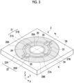
- Fig. 3 is an external perspective view of the MMD 2.
- Fig. 4 is a plan view of the MMD 2 as viewed from the light incident side.
- Fig. 5 is a cross-sectional view taken along the line A-A in Fig. 4 .
- Fig. 6 is a cross-sectional view taken along the line B-B in Fig. 4 .
- the MMD 2 has a mirror portion 20, a first actuator 21, a second actuator 22, a support frame 23, a first support portion 24, a second support portion 25, and a fixed portion 26.
- the MMD 2 is a so-called MEMS device.
- the mirror portion 20 has a reflecting surface 20A for reflecting incident light.
- the reflecting surface 20A is formed of a metal thin film such as gold (Au) and aluminum (Al) provided on one surface of the mirror portion 20.
- the reflecting surface 20A is, for example, circular.
- the first actuator 21 is disposed to surround the mirror portion 20.
- the support frame 23 is disposed to surround the mirror portion 20 and the first actuator 21.
- the second actuator 22 is disposed to surround the mirror portion 20, the first actuator 21, and the support frame 23.
- the support frame 23 is not an essential component of the technology of the present disclosure.
- the first support portion 24 connects the mirror portion 20 and the first actuator 21 on the first axis a 1 , and swingably supports the mirror portion 20 around the first axis a 1 .
- the first axis a 1 is located in a plane including the reflecting surface 20A in a case in which the mirror portion 20 is stationary.
- the first support portion 24 is a torsion bar stretched along the first axis a 1 .
- the first support portion 24 is connected to the support frame 23 on the first axis a 1 .
- the second support portion 25 connects the first actuator 21 and the second actuator 22 on the second axis a 2 , and swingably supports the mirror portion 20 and the first actuator 21 around the second axis a 2 .
- the second axis a 2 is orthogonal to the first axis a 1 in the plane including the reflecting surface 20A in a case in which the mirror portion 20 is stationary.
- the second support portion 25 is connected to the support frame 23 and the fixed portion 26 on the second axis a 2 .
- the fixed portion 26 is connected to the second actuator 22 by the second support portion 25.
- the fixed portion 26 has a rectangular outer shape and surrounds the second actuator 22. Lengths of the fixed portion 26 in the X direction and the Y direction are, for example, about 1 mm to 10 mm, respectively. A thickness of the fixed portion 26 in the Z direction is, for example, about 5 ⁇ m to 0.2 mm.
- the first actuator 21 and the second actuator 22 are piezoelectric actuators each comprising a piezoelectric element.
- the first actuator 21 applies rotational torque around the first axis a 1 to the mirror portion 20.
- the second actuator 22 applies rotational torque around the second axis a 2 to the mirror portion 20 and the first actuator 21. Thereby, the mirror portion 20 swings around the first axis a 1 and the second axis a 2 .
- the first actuator 21 is an annular thin plate member that surrounds the mirror portion 20 in an XY plane.
- the first actuator 21 is composed of a pair of a first movable portion 21A and a second movable portion 21B.
- Each of the first movable portion 21A and the second movable portion 21B is semi-annular.
- the first movable portion 21A and the second movable portion 21B have a shape that is line-symmetrical with respect to the first axis a 1 , and are connected on the first axis a 1 .
- the support frame 23 is an annular thin plate member that surrounds the mirror portion 20 and the first actuator 21 in the XY plane.
- the second actuator 22 is an annular thin plate member that surrounds the mirror portion 20, the first actuator 21, and the support frame 23 in the XY plane.
- the second actuator 22 is composed of a pair of a first movable portion 22A and a second movable portion 22B. Each of the first movable portion 22A and the second movable portion 22B is semi-annular.
- the first movable portion 22A and the second movable portion 22B have a shape that is line-symmetrical with respect to the second axis a 2 , and are connected on the second axis a 2 .
- the first movable portion 21A and the second movable portion 21B are provided with a piezoelectric element 27A and a piezoelectric element 27B, respectively.
- the first movable portion 22A and the second movable portion 22B are provided with a piezoelectric element 28A and a piezoelectric element 28B, respectively.
- a wiring line and an electrode pad for providing the driving signal to the piezoelectric elements 27A, 27B, 28A, and 28B are not shown.
- a plurality of the electrode pads are provided on the fixed portion 26.
- the MMD 2 is formed, for example, by performing an etching treatment on a silicon on insulator (SOI) substrate 30.
- SOI substrate 30 is a substrate in which a silicon oxide layer 32 is provided on a first silicon active layer 31 made of single crystal silicon, and a second silicon active layer 33 made of single crystal silicon is provided on the silicon oxide layer 32.
- the mirror portion 20, the first actuator 21, the second actuator 22, the support frame 23, the first support portion 24, and the second support portion 25 are formed of the second silicon active layer 33 remaining by removing the first silicon active layer 31 and the silicon oxide layer 32 from the SOI substrate 30 by an etching treatment.
- the second silicon active layer 33 functions as an elastic portion having elasticity.
- the fixed portion 26 is formed of three layers of the first silicon active layer 31, the silicon oxide layer 32, and the second silicon active layer 33.
- the piezoelectric elements 27A, 27B, 28A, and 28B have a laminated structure in which a lower electrode 51, a piezoelectric film 52, and an upper electrode 53 are sequentially laminated on the second silicon active layer 33.
- An insulating film is provided on the upper electrode 53, but is not shown.
- the upper electrode 53 and the lower electrode 51 are formed of, for example, gold (Au) or platinum (Pt).
- the piezoelectric film 52 is formed of, for example, lead zirconate titanate (PZT), which is a piezoelectric material.
- PZT lead zirconate titanate
- a driving voltage is applied to the upper electrode 53 from the driving controller 4.
- the lower electrode 51 is connected to the driving controller 4 via the wiring line and the electrode pad, and a reference potential (for example, a ground potential) is applied thereto.
- the piezoelectric film 52 exerts a so-called inverse piezoelectric effect.
- the piezoelectric film 52 exerts an inverse piezoelectric effect by applying a driving voltage from the driving controller 4 to the upper electrode 53, and displaces the first actuator 21 and the second actuator 22.
- Fig. 7 shows a state in which the first actuator 21 is driven by extending one of the piezoelectric films 52 of the first movable portion 21A and the second movable portion 21B and contracting the other piezoelectric film 52.
- the first movable portion 21A and the second movable portion 21B are displaced in opposite directions to each other, whereby the mirror portion 20 rotates around the first axis a 1 .
- Fig. 7 shows an example in which the first actuator 21 is driven in an anti-phase resonance mode in which the displacement direction of the first movable portion 21A and the second movable portion 21B and the rotation direction of the mirror portion 20 are opposite to each other.
- the first movable portion 21A is displaced in the -Z direction and the second movable portion 21B is displaced in the +Z direction, so that the mirror portion 20 rotates in the +Y direction.
- the first actuator 21 may be driven in an in-phase resonance mode in which the displacement direction of the first movable portion 21A and the second movable portion 21B and the rotation direction of the mirror portion 20 are the same direction.
- first deflection angle ⁇ 1 An angle at which a normal line N of the reflecting surface 20A of the mirror portion 20 is inclined in the YZ plane is called a first deflection angle ⁇ 1 .
- the first deflection angle ⁇ 1 takes a positive value
- the first deflection angle ⁇ 1 takes a negative value.
- the first deflection angle ⁇ 1 is controlled by the driving signal (hereinafter, referred to as a first driving signal) provided to the first actuator 21 by the driving controller 4.
- the first driving signal is, for example, a sinusoidal AC voltage.
- the first driving signal includes a driving voltage waveform V 1A (t) applied to the first movable portion 21A and a driving voltage waveform V 1B (t) applied to the second movable portion 21B.
- the driving voltage waveform V 1A (t) and the driving voltage waveform V 1B (t) are in an anti-phase with each other (that is, the phase difference is 180°).
- Fig. 8 shows an example in which the second actuator 22 is driven in an anti-phase resonance mode in which the displacement direction of the first movable portion 22A and the second movable portion 22B and the rotation direction of the mirror portion 20 are opposite to each other.
- the first movable portion 22A is displaced in the -Z direction and the second movable portion 22B is displaced in the +Z direction, so that the mirror portion 20 rotates in the +X direction.
- the second actuator 22 may be driven in an in-phase resonance mode in which the displacement direction of the first movable portion 22A and the second movable portion 22B and the rotation direction of the mirror portion 20 are the same direction.
- An angle at which the normal line N of the reflecting surface 20A of the mirror portion 20 is inclined in the XZ plane is called a second deflection angle ⁇ 2 .
- the second deflection angle ⁇ 2 takes a positive value, and in a case in which it is inclined in the -X direction, the second deflection angle ⁇ 2 takes a negative value.
- the second deflection angle ⁇ 2 is controlled by the driving signal (hereinafter, referred to as a second driving signal) provided to the second actuator 22 by the driving controller 4.
- the second driving signal is, for example, a sinusoidal AC voltage.
- the second driving signal includes a driving voltage waveform V 2A (t) applied to the first movable portion 22A and a driving voltage waveform V 2B (t) applied to the second movable portion 22B.
- the driving voltage waveform V 2A (t) and the driving voltage waveform V 2B (t) are in an anti-phase with each other (that is, the phase difference is 180°).
- Fig. 9 shows an example of a driving signal provided to the first actuator 21 and the second actuator 22.
- A) of Fig. 9 shows the driving voltage waveforms V 1A (t) and V 1B (t) included in the first driving signal.
- B) of Fig. 9 shows the driving voltage waveforms V 2A (t) and V 2B (t) included in the second driving signal.
- V 1A (t) and V 1B (t) are represented as follows, respectively.
- V 1 A t V off1 + V 1 sin 2 ⁇ f d t
- V 1 B t V off1 + V 1 sin 2 ⁇ f d t + ⁇
- V 1 is the amplitude voltage.
- V off1 is the bias voltage.
- f d is the driving frequency.
- t is time.
- the mirror portion 20 swings around the first axis a 1 (see Fig. 7 ).
- V 2A (t) and V 2B (t) are represented as follows, respectively.
- V 2A t V off2 + V 2 sin 2 ⁇ f d t + ⁇
- V 2B t V off2 + V 2 sin 2 ⁇ f d t + ⁇ + ⁇
- V 2 is the amplitude voltage.
- V off2 is the bias voltage.
- f d is the driving frequency.
- t is time.
- ⁇ is the phase difference between the driving voltage waveforms V 1A (t) and V 1B (t) and the driving voltage waveforms V 2A (t) and V 2B (t).
- ⁇ 90° is set in order to cause the mirror portion 20 to perform precession.
- the bias voltages V off1 and V off2 are DC voltages for determining a state where the mirror portion 20 is stationary.
- a plane including the reflecting surface 20A may not be parallel to an upper surface of the fixed portion 26 and may be inclined with respect to the upper surface of the fixed portion 26.
- the mirror portion 20 swings around the second axis a 2 (see Fig. 8 ).
- the first driving signal and the second driving signal have the same driving frequency f d and a phase difference of 90°.
- the meaning of "match” includes not only the meaning of perfect match but also the meaning of substantial match including allowable errors in design and manufacturing.
- the maximum deflection angle ⁇ m1 of the first deflection angle ⁇ 1 is referred to as a first maximum deflection angle ⁇ m1 .
- the maximum deflection angle ⁇ m2 of the second deflection angle ⁇ 2 is referred to as a second maximum deflection angle ⁇ m2 .
- a maximum deflection angle ⁇ m is simply referred to as a maximum deflection angle ⁇ m .
- Fig. 11 shows the precession of the mirror portion 20.
- the precession is a motion in which the normal line N of the reflecting surface 20A of the mirror portion 20 is deflected such that a circle is drawn.
- Fig. 12 schematically shows an example of a relationship between the deflection angle of the mirror portion 20 and the driving frequency f d .
- the mirror portion 20 vibrates around the first axis a 1 and the second axis a 2 at a natural vibration frequency.
- the mirror portion 20 resonates in a case in which the driving frequency f d matches the natural vibration frequency.
- f 1 represents a resonance frequency (hereinafter, referred to as a first resonance frequency) around the first axis a 1 of the mirror portion 20.
- f 2 represents a resonance frequency (hereinafter, referred to as a second resonance frequency) around the second axis a 2 of the mirror portion 20.
- the first resonance frequency f 1 is a resonance frequency in a case in which the mirror portion 20 swings only around the first axis a 1 without swinging around the second axis a 2 .
- the second resonance frequency f 2 is a resonance frequency in a case in which the mirror portion 20 swings only around the second axis a 2 without swinging around the first axis a 1 .
- a plurality of resonance modes exist for the swing of the mirror portion 20 in addition to the phase (in-phase or anti-phase) with the movable portion described above.
- the first resonance frequency f 1 and the second resonance frequency f 2 are in an anti-phase and are resonance frequencies in the lowest order (that is, the lowest frequency) resonance mode.
- the first resonance frequency f 1 and the second resonance frequency f 2 can be set by adjusting an inertial moment, a spring constant, and the like of the components of the MMD 2 in terms of design.
- the crosstalk is caused by the fact that propagation of vibration generated in one of the first actuator 21 and the second actuator 22 to the other excites resonance vibration.
- an influence of the crosstalk is greatly exerted, particularly in a case in which the maximum deflection angle ⁇ m of the mirror portion 20 is small, that is, in a case in which the driving signal is small.
- the first actuator 21 allows the mirror portion 20 to swing around the first axis a 1 and the second actuator 22 allows the first actuator 21 to swing around the second axis a 2 together with the mirror portion 20.
- the first actuator 21 also swings around the second axis a 2 , so that a vibration component around the second axis a 2 propagates to the first axis a 1 , which affects a change in voltage characteristics of the first actuator 21 and the first resonance frequency f 1 .
- the present applicant confirmed that the first resonance frequency f 1 shifts in a case in which the mirror portion 20 swings around the first axis a 1 and around the second axis a 2 simultaneously.
- this shift amount will be denoted by ⁇ f.
- the first resonance frequency f 1 is not matched with the second resonance frequency f 2 .
- a magnitude relationship between the first resonance frequency f 1 and the second resonance frequency f 2 needs to be determined in consideration of the shift amount ⁇ f. This is because the shift amount ⁇ f changes depending on a magnitude of the maximum deflection angle ⁇ m of the mirror portion 20.
- Fig. 13 shows an example of a change in the shift amount ⁇ f with respect to the maximum deflection angle ⁇ m of the mirror portion 20.
- the present applicant measured the shift amount ⁇ f of the first resonance frequency f 1 with respect to the maximum deflection angle ⁇ m in a case in which the surface to be scanned 5 was scanned with the light beam L such that a positive circle is drawn on the surface to be scanned 5 by causing the mirror portion 20 to perform precession.
- a size of the circle scanned on the surface to be scanned 5 is proportional to the maximum deflection angle ⁇ m .
- the shift amount ⁇ f of the first resonance frequency f 1 increased as the maximum deflection angle ⁇ m increased.
- the shift amount ⁇ f was a positive value (that is, ⁇ f > 0).
- the deflection angle can be improved with low power in a case in which the first resonance frequency f 1 and the second resonance frequency f 2 satisfy a relationship of "f 2 ⁇ f 1 " and the driving frequency f d satisfies a relationship of "f d ⁇ f 1 ".
- a radius of a circle scanned on the surface to be scanned 5 by the light beam L (hereinafter, referred to as a scanning radius) is controlled.
- This scanning radius corresponds to the maximum deflection angle ⁇ m of the mirror portion 20.
- the first maximum deflection angle ⁇ m1 depends on the amplitude voltage V 1 of the first driving signal.
- the second maximum deflection angle ⁇ m2 depends on the amplitude voltage V 2 of the second driving signal.
- the maximum deflection angle ⁇ m is 10° or more.
- the amplitude voltage V 1 and the amplitude voltage V 2 are each less than 40 V.
- the measurement results of the maximum deflection angle ⁇ m of the mirror portion 20 and the amplitude voltages V 1 and V 2 are shown below.
- the present applicant measured a relationship between the amplitude voltages V 1 and V 2 with respect to the radius of the circle (scanning radius) in a case in which the surface to be scanned 5 was scanned with the light beam L such that a positive circle is drawn on the surface to be scanned 5 by causing the mirror portion 20 to perform precession.
- the surface to be scanned 5 was provided with gradations at intervals of 1 mm, and the maximum deflection angle ⁇ m was measured based on a measured value of a shape and size of the circle using the gradations.
- Fig. 14 shows a measurement result of the maximum deflection angle ⁇ m in a case where the driving frequency f d is set in a range of f d ⁇ f 1 - ⁇ f.
- f d f 1 - 25 Hz.
- Fig. 15 shows a measurement result of the maximum deflection angle ⁇ m in a case in which the driving frequency f d is set in a range of f 1 - ⁇ f ⁇ f d ⁇ f 2 .
- Fig. 17 shows a measurement result of the maximum deflection angle ⁇ m in a case in which the driving frequency f d is set in a range of f 2 ⁇ f d ⁇ f 1 .
- Fig. 18 shows a measurement result of the maximum deflection angle ⁇ m in a case in which the driving frequency f d is set in a range of f 1 ⁇ f d .
- Fig. 17 it can be seen that ⁇ m1 ⁇ 10° in a case of V 1 >_ 50 V and ⁇ m2 ⁇ 10° in a case of V 2 >_ 32 V.
- the driving frequency f d satisfies the relationship of "f d ⁇ f 1 " in order to improve the deflection angle with low power. Further, it can be seen that it is more preferable that the driving frequency f d satisfies a relationship of "f 1 - ⁇ f ⁇ f d ⁇ f 2 ". That is, it is not preferable that the driving frequency f d is too far from f 1 - ⁇ f and f 2 , but it is preferable that the driving frequency f d is within a range between f 1 - ⁇ f and f 2 .
- An MMD 2A shown in Figs. 19 and 20 has a rib 60 on a back surface side (that is, a side opposite to the light incident side) of the mirror portion 20.
- Fig. 19 is a plan view of the MMD 2A as viewed from the back surface side.
- Fig. 20 is a cross-sectional view taken along the line C-C of Fig. 19 .
- Other configurations of the MMD 2A are the same as those of the MMD 2 according to the above-described embodiment.
- the rib 60 increases the rigidity of the mirror portion 20 to increase the flatness of the reflecting surface 20A formed on the light incident side of the mirror portion 20.
- the rib 60 is formed by patterning the first silicon active layer 31 and the silicon oxide layer 32 by an etching treatment.
- a planar shape of the rib 60 is an elliptical shape in which the center coincides with the center of the mirror portion 20.
- a minor axis is parallel to the first axis a 1 and the major axis is parallel to the second axis a 2 .
- a ratio of the minor diameter D1 to the major diameter D2 a ratio of the first resonance frequency f 1 to the second resonance frequency f 2 can be adjusted to satisfy the relationship of "f 2 ⁇ f 1 ".
- first actuator 21 and the second actuator 22 have an annular shape
- one or both of the first actuator 21 and the second actuator 22 may have a meander structure.
- a processing unit of the driving controller 4 may be configured of one processor, or may be configured of a combination of two or more processors of the same type or different types (for example, a combination of a plurality of field programmable gate arrays (FPGAs) and/or a combination of a CPU and an FPGA).
- FPGAs field programmable gate arrays
Abstract
An optical scanning device includes: a micromirror device including a mirror portion that has a reflecting surface for reflecting incident light, a first actuator that allows the mirror portion to swing around a first axis located in a plane including the reflecting surface in a case in which the mirror portion is stationary, and a second actuator that allows the mirror portion to swing around a second axis orthogonal to the first axis in the plane; and a processor that causes the mirror portion to perform precession by providing a first driving signal and a second driving signal each having the same driving frequency to the first actuator and the second actuator, respectively. In the micromirror device, a relationship of f<sub>2</sub> < f<sub>1</sub> is satisfied in a case in which a resonance frequency around the first axis is denoted by f<sub>1</sub> and a resonance frequency around the second axis is denoted by f<sub>2</sub>, and a relationship of f<sub>d</sub> ≤ f<sub>1</sub> is satisfied in a case in which the driving frequency is denoted by f<sub>d</sub>.
Description
- The technology of the present disclosure relates to an optical scanning device and a method of driving a micromirror device.
- A micromirror device (also referred to as a microscanner) is known as one of micro electro mechanical systems (MEMS) devices manufactured using the silicon (Si) nanofabrication technique. The micromirror device is driven by a driving controller provided in an optical scanning device. By driving a mirror portion of the micromirror device, the driving controller two-dimensionally scans an object with a light beam reflected by the mirror portion.
- An optical scanning method using the micromirror device is superior to an optical scanning method using a polygon mirror in the related art in terms of small size, light weight, and low power consumption. Therefore, application of the micromirror device to a light detection and ranging (LiDAR) device, a scanning beam display, and the like is attracting attention.
- Examples of a drive method of the micromirror device include an electrostatic drive method, an electromagnetic drive method, and a piezoelectric drive method. In the piezoelectric drive method, the device has a small size and has a large scan angle because a device structure and a drive circuit are simple while torque is large. The micromirror device resonates at a natural vibration frequency determined by a mass, structure, and spring constant. By driving the micromirror device at the resonance frequency, a larger scan angle is obtained. The scan angle corresponds to a deflection angle of the mirror portion.
-
WO2018/230065A proposes a piezoelectric biaxial drive type micromirror device that enables precession of a mirror portion. The precession is a motion in which a central axis orthogonal to a reflecting surface of the mirror portion is deflected such that a circle is drawn. In order to cause the mirror portion to perform precession, it is necessary to allow the mirror portion to swing around each of a first axis and a second axis orthogonal to each other at the same frequency. Therefore,WO2018/230065A proposes matching a resonance frequency around the first axis (hereinafter, referred to as a first resonance frequency) with a resonance frequency around the second axis (hereinafter, referred to as a second resonance frequency). - By the precession of the mirror portion, an object to be scanned is scanned with a light beam reflected by the mirror portion such that a circle is drawn. The circular light beam is used, for example, in the LiDAR device.
-
JP2019-144497A - As disclosed in
WO2018/230065A , by matching the first resonance frequency with the second resonance frequency and matching frequencies of driving signals provided to first and second actuators with the first resonance frequency and the second resonance frequency, responsiveness of an operation of the mirror portion to the driving signals is improved. However, in a case in which the first resonance frequency is matched with the second resonance frequency, it is considered that there is an adverse effect that the crosstalk disclosed inJP2019-144497A - The present applicant has confirmed that crosstalk is likely to occur in a micromirror device in which the first actuator allows the mirror portion to swing around the first axis and the second actuator allows the first actuator to swing around the second axis together with the mirror portion. Specifically, the present applicant has confirmed that the first resonance frequency shifts according to a deflection angle around the second axis.
- In order to cause the mirror portion to perform precession, it is necessary to accurately match a deflection angle around the first axis with a deflection angle around the second axis. However, in a case in which the above-mentioned crosstalk occurs, the first resonance frequency shifts according to the deflection angle around the second axis, so that the deflection angle around the first axis is lowered.
- In order to improve the deflection angle, it is conceivable to increase the amplitude voltage of the driving signal. However, in a case in which the amplitude voltage of the driving signal is increased, there is an adverse effect that a drive circuit for driving the micromirror device is increased in size and the power consumption is increased.
- An object of the technology of the present disclosure is to provide an optical scanning device that can improve a deflection angle with low power in a case in which a mirror portion performs precession, and a method of driving a micromirror device.
- In order to achieve the above-described object, an optical scanning device of the present disclosure comprises: a micromirror device including a mirror portion that has a reflecting surface for reflecting incident light, a first actuator that allows the mirror portion to swing around a first axis located in a plane including the reflecting surface in a case in which the mirror portion is stationary, and a second actuator that allows the mirror portion to swing around a second axis orthogonal to the first axis in the plane; and a processor that causes the mirror portion to perform precession by providing a first driving signal and a second driving signal each having the same driving frequency to the first actuator and the second actuator, respectively, in which, in the micromirror device, a relationship of f2 < f1 is satisfied in a case in which a resonance frequency around the first axis is denoted by f1 and a resonance frequency around the second axis is denoted by f2, and a relationship of fd ≤ f1 is satisfied in a case in which the driving frequency is denoted by fd.
- It is preferable that in a case in which the mirror portion is driven around the first axis and the second axis simultaneously, the resonance frequency around the first axis changes by Δf from f1, and that a relationship of f1-Δf < fd is satisfied.
- It is preferable that a relationship of Δf > 0 is satisfied.
- It is preferable that a relationship of f1-Δf < fd < f2 is satisfied.
- It is preferable that the first actuator and the second actuator are piezoelectric actuators each including a piezoelectric element.
- It is preferable that the first actuator is connected to the mirror portion via a first support portion that swingably supports the mirror portion around the first axis, and that the second actuator is connected to the first actuator via a second support portion that swingably supports the first actuator around the second axis.
- It is preferable that each of the first support portion and the second support portion is a torsion bar.
- It is preferable that the optical scanning device further comprises a light source that emits a light beam perpendicularly to the reflecting surface in a case in which the mirror portion is stationary.
- A method of driving a micromirror device of the present disclosure is a method of driving a micromirror device including a mirror portion that has a reflecting surface for reflecting incident light, a first actuator that allows the mirror portion to swing around a first axis located in a plane including the reflecting surface in a case in which the mirror portion is stationary, and a second actuator that allows the mirror portion to swing around a second axis orthogonal to the first axis in the plane. In the micromirror device, a relationship of f2 < f1 is satisfied in a case in which a resonance frequency around the first axis is denoted by f1 and a resonance frequency around the second axis is denoted by f2, and a first driving signal and a second driving signal each having a driving frequency fd satisfying a relationship of fd < f1 are provided to the first actuator and the second actuator, respectively, to cause the mirror portion to perform precession.
- According to the technology of the present disclosure, it is possible to provide an optical scanning device that can improve a deflection angle with low power in a case in which a mirror portion performs precession, and a method of driving a micromirror device.
-
-
Fig. 1 is a schematic view of an optical scanning device. -
Fig. 2 is a block diagram showing an example of a hardware configuration of a driving controller. -
Fig. 3 is an external perspective view of a micromirror device. -
Fig. 4 is a plan view of the micromirror device as viewed from the light incident side. -
Fig. 5 is a cross-sectional view taken along the line A-A ofFig. 4 . -
Fig. 6 is a cross-sectional view taken along the line B-B ofFig. 4 . -
Fig. 7 is a diagram showing an example in which a first actuator is driven in an anti-phase resonance mode. -
Fig. 8 is a diagram showing an example in which a second actuator is driven in an anti-phase resonance mode. -
Fig. 9 is a diagram showing an example of a driving signal provided to the first actuator and the second actuator. -
Fig. 10 is a diagram illustrating a time change of a maximum deflection angle. -
Fig. 11 is a diagram illustrating precession of a mirror portion. -
Fig. 12 is a diagram schematically showing a relationship between a deflection angle and a driving frequency. -
Fig. 13 is a diagram showing an example of a change in a shift amount with respect to a maximum deflection angle. -
Fig. 14 is a diagram showing a measurement result of a maximum deflection angle in a case in which a driving frequency fd is set in a range of fd < f1-Δf. -
Fig. 15 is a diagram showing a measurement result of a maximum deflection angle in a case in which the driving frequency fd is set in a range of f1-Δf < fd < f2. -
Fig. 16 is a diagram showing a measurement result of a maximum deflection angle in a case in which the driving frequency fd is set as fd = f2. -
Fig. 17 is a diagram showing a measurement result of a maximum deflection angle in a case in which the driving frequency fd is set in a range of f2 < fd ≤ f1. -
Fig. 18 is a diagram showing a measurement result of a maximum deflection angle in a case in which the driving frequency fd is set in a range of f1 < fd. -
Fig. 19 is a plan view of a micromirror device having a rib as viewed from a back surface side. -
Fig. 20 is a cross-sectional view taken along the line C-C ofFig. 19 . - An example of an embodiment relating to the technology of the present disclosure will be described with reference to the accompanying drawings.
-
Fig. 1 schematically shows anoptical scanning device 10 according to an embodiment. Theoptical scanning device 10 includes a micromirror device (hereinafter, referred to as micromirror device (MMD)) 2, alight source 3, and a drivingcontroller 4. Theoptical scanning device 10 optically scans a surface to be scanned 5 by reflecting a light beam L emitted from thelight source 3 by theMMD 2 under the control of the drivingcontroller 4. The surface to be scanned 5 is, for example, a screen. - The
MMD 2 is a piezoelectric biaxial drive type micromirror device capable of allowing a mirror portion 20 (seeFig. 3 ) to swing around a first axis a1 and a second axis a2 orthogonal to the first axis a1. Hereinafter, the direction parallel to the first axis a1 is referred to as an X direction, the direction parallel to the second axis a2 is a Y direction, and the direction orthogonal to the first axis a1 and the second axis a2 is referred to as a Z direction. - The
light source 3 is a laser device that emits, for example, laser light as the light beam L. It is preferable that thelight source 3 emits the light beam L perpendicularly to a reflectingsurface 20A (seeFig. 3 ) included in themirror portion 20 in a state where themirror portion 20 of theMMD 2 is stationary. - The driving
controller 4 outputs a driving signal to thelight source 3 and theMMD 2 based on optical scanning information. Thelight source 3 generates the light beam L based on the input driving signal and emits the light beam L to theMMD 2. TheMMD 2 allows themirror portion 20 to swing around the first axis a1 and the second axis a2 based on the input driving signal. - As will be described in detail below, the driving
controller 4 causes themirror portion 20 to perform precession. By the precession of themirror portion 20, the surface to be scanned 5 is scanned with the light beam L reflected by themirror portion 20 such that a circle is drawn on the surface to be scanned 5. The circular light beam L is used, for example, in the LiDAR device. -
Fig. 2 shows an example of a hardware configuration of the drivingcontroller 4. The drivingcontroller 4 has a central processing unit (CPU) 40, a read only memory (ROM) 41, a random access memory (RAM) 42, alight source driver 43, and anMMD driver 44. TheCPU 40 is an arithmetic unit that realizes the entire function of the drivingcontroller 4 by reading out a program and data from a storage device such as the ROM 41 into theRAM 42 and executing processing. TheCPU 40 is an example of a "processor" according to the technology of the present disclosure. - The ROM 41 is a non-volatile storage device and stores a program for the
CPU 40 to execute processing and data such as the optical scanning information described above. TheRAM 42 is a non-volatile storage device that temporarily holds a program and data. - The
light source driver 43 is an electric circuit that outputs a driving signal to thelight source 3 under the control of theCPU 40. In thelight source driver 43, the driving signal is a driving voltage for controlling the irradiation timing and the irradiation intensity of thelight source 3. - The
MMD driver 44 is an electric circuit that outputs a driving signal to theMMD 2 under the control of theCPU 40. In theMMD driver 44, the driving signal is a driving voltage for controlling the timing, cycle, and deflection angle for allowing themirror portion 20 of theMMD 2 to swing. - The
CPU 40 controls thelight source driver 43 and theMMD driver 44 based on the optical scanning information. The optical scanning information is information for indicating how the surface to be scanned 5 is scanned with the light beam L. In the present embodiment, the optical scanning information is information for indicating that the surface to be scanned 5 is scanned with the light beam L such that a circle is drawn on the surface to be scanned 5. For example, in a case in which theoptical scanning device 10 is incorporated in the LiDAR device, the optical scanning information includes a time at which the light beam L for distance measurement is emitted, an irradiation range, and the like. - Next, an example of the
MMD 2 will be described with reference toFigs. 3 to 6 .Fig. 3 is an external perspective view of theMMD 2.Fig. 4 is a plan view of theMMD 2 as viewed from the light incident side.Fig. 5 is a cross-sectional view taken along the line A-A inFig. 4 .Fig. 6 is a cross-sectional view taken along the line B-B inFig. 4 . - As shown in
Figs. 3 and4 , theMMD 2 has amirror portion 20, afirst actuator 21, asecond actuator 22, asupport frame 23, afirst support portion 24, asecond support portion 25, and a fixedportion 26. TheMMD 2 is a so-called MEMS device. - The
mirror portion 20 has a reflectingsurface 20A for reflecting incident light. The reflectingsurface 20A is formed of a metal thin film such as gold (Au) and aluminum (Al) provided on one surface of themirror portion 20. The reflectingsurface 20A is, for example, circular. - The
first actuator 21 is disposed to surround themirror portion 20. Thesupport frame 23 is disposed to surround themirror portion 20 and thefirst actuator 21. Thesecond actuator 22 is disposed to surround themirror portion 20, thefirst actuator 21, and thesupport frame 23. Thesupport frame 23 is not an essential component of the technology of the present disclosure. - The
first support portion 24 connects themirror portion 20 and thefirst actuator 21 on the first axis a1, and swingably supports themirror portion 20 around the first axis a1. The first axis a1 is located in a plane including the reflectingsurface 20A in a case in which themirror portion 20 is stationary. For example, thefirst support portion 24 is a torsion bar stretched along the first axis a1. In addition, thefirst support portion 24 is connected to thesupport frame 23 on the first axis a1. - The
second support portion 25 connects thefirst actuator 21 and thesecond actuator 22 on the second axis a2, and swingably supports themirror portion 20 and thefirst actuator 21 around the second axis a2. The second axis a2 is orthogonal to the first axis a1 in the plane including the reflectingsurface 20A in a case in which themirror portion 20 is stationary. Thesecond support portion 25 is connected to thesupport frame 23 and the fixedportion 26 on the second axis a2. - The fixed
portion 26 is connected to thesecond actuator 22 by thesecond support portion 25. The fixedportion 26 has a rectangular outer shape and surrounds thesecond actuator 22. Lengths of the fixedportion 26 in the X direction and the Y direction are, for example, about 1 mm to 10 mm, respectively. A thickness of the fixedportion 26 in the Z direction is, for example, about 5 µm to 0.2 mm. - The
first actuator 21 and thesecond actuator 22 are piezoelectric actuators each comprising a piezoelectric element. Thefirst actuator 21 applies rotational torque around the first axis a1 to themirror portion 20. Thesecond actuator 22 applies rotational torque around the second axis a2 to themirror portion 20 and thefirst actuator 21. Thereby, themirror portion 20 swings around the first axis a1 and the second axis a2. - The
first actuator 21 is an annular thin plate member that surrounds themirror portion 20 in an XY plane. Thefirst actuator 21 is composed of a pair of a firstmovable portion 21A and a secondmovable portion 21B. Each of the firstmovable portion 21A and the secondmovable portion 21B is semi-annular. The firstmovable portion 21A and the secondmovable portion 21B have a shape that is line-symmetrical with respect to the first axis a1, and are connected on the first axis a1. - The
support frame 23 is an annular thin plate member that surrounds themirror portion 20 and thefirst actuator 21 in the XY plane. - The
second actuator 22 is an annular thin plate member that surrounds themirror portion 20, thefirst actuator 21, and thesupport frame 23 in the XY plane. Thesecond actuator 22 is composed of a pair of a firstmovable portion 22A and a secondmovable portion 22B. Each of the firstmovable portion 22A and the secondmovable portion 22B is semi-annular. The firstmovable portion 22A and the secondmovable portion 22B have a shape that is line-symmetrical with respect to the second axis a2, and are connected on the second axis a2. - In the
first actuator 21, the firstmovable portion 21A and the secondmovable portion 21B are provided with apiezoelectric element 27A and apiezoelectric element 27B, respectively. In addition, in thesecond actuator 22, the firstmovable portion 22A and the secondmovable portion 22B are provided with apiezoelectric element 28A and apiezoelectric element 28B, respectively. - In
Figs. 3 and4 , a wiring line and an electrode pad for providing the driving signal to thepiezoelectric elements portion 26. - As shown in
Figs. 5 and6 , theMMD 2 is formed, for example, by performing an etching treatment on a silicon on insulator (SOI)substrate 30. TheSOI substrate 30 is a substrate in which asilicon oxide layer 32 is provided on a first siliconactive layer 31 made of single crystal silicon, and a second siliconactive layer 33 made of single crystal silicon is provided on thesilicon oxide layer 32. - The
mirror portion 20, thefirst actuator 21, thesecond actuator 22, thesupport frame 23, thefirst support portion 24, and thesecond support portion 25 are formed of the second siliconactive layer 33 remaining by removing the first siliconactive layer 31 and thesilicon oxide layer 32 from theSOI substrate 30 by an etching treatment. The second siliconactive layer 33 functions as an elastic portion having elasticity. The fixedportion 26 is formed of three layers of the first siliconactive layer 31, thesilicon oxide layer 32, and the second siliconactive layer 33. - The
piezoelectric elements lower electrode 51, apiezoelectric film 52, and anupper electrode 53 are sequentially laminated on the second siliconactive layer 33. An insulating film is provided on theupper electrode 53, but is not shown. - The
upper electrode 53 and thelower electrode 51 are formed of, for example, gold (Au) or platinum (Pt). Thepiezoelectric film 52 is formed of, for example, lead zirconate titanate (PZT), which is a piezoelectric material. Theupper electrode 53 and thelower electrode 51 are electrically connected to the drivingcontroller 4 described above via the wiring line and the electrode pad. - A driving voltage is applied to the
upper electrode 53 from the drivingcontroller 4. Thelower electrode 51 is connected to the drivingcontroller 4 via the wiring line and the electrode pad, and a reference potential (for example, a ground potential) is applied thereto. - In a case in which a positive or negative voltage is applied to the
piezoelectric film 52 in the polarization direction, deformation (for example, expansion and contraction) proportional to the applied voltage occurs. That is, thepiezoelectric film 52 exerts a so-called inverse piezoelectric effect. Thepiezoelectric film 52 exerts an inverse piezoelectric effect by applying a driving voltage from the drivingcontroller 4 to theupper electrode 53, and displaces thefirst actuator 21 and thesecond actuator 22. -
Fig. 7 shows a state in which thefirst actuator 21 is driven by extending one of thepiezoelectric films 52 of the firstmovable portion 21A and the secondmovable portion 21B and contracting the otherpiezoelectric film 52. In this way, the firstmovable portion 21A and the secondmovable portion 21B are displaced in opposite directions to each other, whereby themirror portion 20 rotates around the first axis a1. -
Fig. 7 shows an example in which thefirst actuator 21 is driven in an anti-phase resonance mode in which the displacement direction of the firstmovable portion 21A and the secondmovable portion 21B and the rotation direction of themirror portion 20 are opposite to each other. InFig. 7 , the firstmovable portion 21A is displaced in the -Z direction and the secondmovable portion 21B is displaced in the +Z direction, so that themirror portion 20 rotates in the +Y direction. Thefirst actuator 21 may be driven in an in-phase resonance mode in which the displacement direction of the firstmovable portion 21A and the secondmovable portion 21B and the rotation direction of themirror portion 20 are the same direction. - An angle at which a normal line N of the reflecting
surface 20A of themirror portion 20 is inclined in the YZ plane is called a first deflection angle θ1. In a case in which the normal line N of the reflectingsurface 20A is inclined in the +Y direction, the first deflection angle θ1 takes a positive value, and in a case in which it is inclined in the -Y direction, the first deflection angle θ1 takes a negative value. - The first deflection angle θ1 is controlled by the driving signal (hereinafter, referred to as a first driving signal) provided to the
first actuator 21 by the drivingcontroller 4. The first driving signal is, for example, a sinusoidal AC voltage. The first driving signal includes a driving voltage waveform V1A (t) applied to the firstmovable portion 21A and a driving voltage waveform V1B (t) applied to the secondmovable portion 21B. The driving voltage waveform V1A (t) and the driving voltage waveform V1B (t) are in an anti-phase with each other (that is, the phase difference is 180°). -
Fig. 8 shows an example in which thesecond actuator 22 is driven in an anti-phase resonance mode in which the displacement direction of the firstmovable portion 22A and the secondmovable portion 22B and the rotation direction of themirror portion 20 are opposite to each other. InFig. 8 , the firstmovable portion 22A is displaced in the -Z direction and the secondmovable portion 22B is displaced in the +Z direction, so that themirror portion 20 rotates in the +X direction. Thesecond actuator 22 may be driven in an in-phase resonance mode in which the displacement direction of the firstmovable portion 22A and the secondmovable portion 22B and the rotation direction of themirror portion 20 are the same direction. - An angle at which the normal line N of the reflecting
surface 20A of themirror portion 20 is inclined in the XZ plane is called a second deflection angle θ2. In a case in which the normal line N of the reflectingsurface 20A is inclined in the +X direction, the second deflection angle θ2 takes a positive value, and in a case in which it is inclined in the -X direction, the second deflection angle θ2 takes a negative value. - The second deflection angle θ2 is controlled by the driving signal (hereinafter, referred to as a second driving signal) provided to the
second actuator 22 by the drivingcontroller 4. The second driving signal is, for example, a sinusoidal AC voltage. The second driving signal includes a driving voltage waveform V2A (t) applied to the firstmovable portion 22A and a driving voltage waveform V2B (t) applied to the secondmovable portion 22B. The driving voltage waveform V2A (t) and the driving voltage waveform V2B (t) are in an anti-phase with each other (that is, the phase difference is 180°). -
Fig. 9 shows an example of a driving signal provided to thefirst actuator 21 and thesecond actuator 22. (A) ofFig. 9 shows the driving voltage waveforms V1A (t) and V1B (t) included in the first driving signal. (B) ofFig. 9 shows the driving voltage waveforms V2A (t) and V2B (t) included in the second driving signal. - The driving voltage waveforms V1A (t) and V1B (t) are represented as follows, respectively.


- Here, V1 is the amplitude voltage. Voff1 is the bias voltage. fd is the driving frequency. t is time. α is the phase difference between the driving voltage waveforms V1A (t) and V1B (t). In the present embodiment, for example, α = 180°.
- By applying the driving voltage waveforms V1A (t) and V1B (t) to the first
movable portion 21A and the secondmovable portion 21B, themirror portion 20 swings around the first axis a1 (seeFig. 7 ). - The driving voltage waveforms V2A (t) and V2B (t) are represented as follows, respectively.


- Here, V2 is the amplitude voltage. Voff2 is the bias voltage. fd is the driving frequency. t is time. β is the phase difference between the driving voltage waveforms V2A (t) and V2B (t). In the present embodiment, for example, β = 180°. In addition, ϕ is the phase difference between the driving voltage waveforms V1A (t) and V1B (t) and the driving voltage waveforms V2A (t) and V2B (t). In the present embodiment, ϕ = 90° is set in order to cause the
mirror portion 20 to perform precession. - The bias voltages Voff1 and Voff2 are DC voltages for determining a state where the
mirror portion 20 is stationary. In a state where themirror portion 20 is stationary, a plane including the reflectingsurface 20A may not be parallel to an upper surface of the fixedportion 26 and may be inclined with respect to the upper surface of the fixedportion 26. - By applying the driving voltage waveforms V2A (t) and V2B (t) to the first
movable portion 22A and the secondmovable portion 22B, themirror portion 20 swings around the second axis a2 (seeFig. 8 ). - As described above, the first driving signal and the second driving signal have the same driving frequency fd and a phase difference of 90°. In order to cause the
mirror portion 20 to perform precession, as shown inFig. 10 , it is necessary to set the amplitude voltages V1 and V2 appropriately such that the maximum deflection angle θm1 of the first deflection angle θ1 matches the maximum deflection angle θm2 of the second deflection angle θ2. This is because a relationship between the amplitude voltage V1 and the first deflection angle θ1 and a relationship between the amplitude voltage V2 and the second deflection angle θ2 are not the same. In the description of the present specification, the meaning of "match" includes not only the meaning of perfect match but also the meaning of substantial match including allowable errors in design and manufacturing. - Hereinafter, the maximum deflection angle θm1 of the first deflection angle θ1 is referred to as a first maximum deflection angle θm1. The maximum deflection angle θm2 of the second deflection angle θ2 is referred to as a second maximum deflection angle θm2. Further, in a case in which the first maximum deflection angle θm1 and the second maximum deflection angle θm2 are not distinguished, it is simply referred to as a maximum deflection angle θm.
- In order to cause the
mirror portion 20 to perform precession with high accuracy, it is necessary to appropriately set the driving frequency fd.Fig. 11 shows the precession of themirror portion 20. The precession is a motion in which the normal line N of the reflectingsurface 20A of themirror portion 20 is deflected such that a circle is drawn. By irradiating themirror portion 20 performing the precession with the light beam L from thelight source 3, the surface to be scanned 5 can be scanned with the light beam L such that a circle is drawn on the surface to be scanned 5. -
Fig. 12 schematically shows an example of a relationship between the deflection angle of themirror portion 20 and the driving frequency fd. Themirror portion 20 vibrates around the first axis a1 and the second axis a2 at a natural vibration frequency. Themirror portion 20 resonates in a case in which the driving frequency fd matches the natural vibration frequency. - In
Fig. 12 , f1 represents a resonance frequency (hereinafter, referred to as a first resonance frequency) around the first axis a1 of themirror portion 20. f2 represents a resonance frequency (hereinafter, referred to as a second resonance frequency) around the second axis a2 of themirror portion 20. The first resonance frequency f1 is a resonance frequency in a case in which themirror portion 20 swings only around the first axis a1 without swinging around the second axis a2. The second resonance frequency f2 is a resonance frequency in a case in which themirror portion 20 swings only around the second axis a2 without swinging around the first axis a1. - A plurality of resonance modes exist for the swing of the
mirror portion 20 in addition to the phase (in-phase or anti-phase) with the movable portion described above. For example, the first resonance frequency f1 and the second resonance frequency f2 are in an anti-phase and are resonance frequencies in the lowest order (that is, the lowest frequency) resonance mode. - The closer the driving frequency fd is to the first resonance frequency f1, the larger the first deflection angle θ1 is. In addition, the closer the driving frequency fd is to the second resonance frequency f2, the larger the second deflection angle θ2 is. Therefore, in general, by matching the first resonance frequency f1 with the second resonance frequency f2 and matching the driving frequency fd with the first resonance frequency f1 and the second resonance frequency f2, the responsiveness of the deflection angle to the driving signal is improved. The first resonance frequency f1 and the second resonance frequency f2 can be set by adjusting an inertial moment, a spring constant, and the like of the components of the
MMD 2 in terms of design. - However, in a case in which the first resonance frequency f1 is matched with the second resonance frequency f2, it is considered that there is an adverse effect that the crosstalk increases. The crosstalk is caused by the fact that propagation of vibration generated in one of the
first actuator 21 and thesecond actuator 22 to the other excites resonance vibration. In a case in which the first resonance frequency f1 is matched with the second resonance frequency f2, an influence of the crosstalk is greatly exerted, particularly in a case in which the maximum deflection angle θm of themirror portion 20 is small, that is, in a case in which the driving signal is small. - In the
MMD 2 of the present embodiment, thefirst actuator 21 allows themirror portion 20 to swing around the first axis a1 and thesecond actuator 22 allows thefirst actuator 21 to swing around the second axis a2 together with themirror portion 20. In this way, in a case in which themirror portion 20 is allowed to swing around the second axis a2, thefirst actuator 21 also swings around the second axis a2, so that a vibration component around the second axis a2 propagates to the first axis a1, which affects a change in voltage characteristics of thefirst actuator 21 and the first resonance frequency f1. The present applicant confirmed that the first resonance frequency f1 shifts in a case in which themirror portion 20 swings around the first axis a1 and around the second axis a2 simultaneously. Hereinafter, this shift amount will be denoted by Δf. - In order to avoid the crosstalk, it is preferable that the first resonance frequency f1 is not matched with the second resonance frequency f2. In addition, a magnitude relationship between the first resonance frequency f1 and the second resonance frequency f2 needs to be determined in consideration of the shift amount Δf. This is because the shift amount Δf changes depending on a magnitude of the maximum deflection angle θm of the
mirror portion 20. -
Fig. 13 shows an example of a change in the shift amount Δf with respect to the maximum deflection angle θm of themirror portion 20. The present applicant measured the shift amount Δf of the first resonance frequency f1 with respect to the maximum deflection angle θm in a case in which the surface to be scanned 5 was scanned with the light beam L such that a positive circle is drawn on the surface to be scanned 5 by causing themirror portion 20 to perform precession. A size of the circle scanned on the surface to be scanned 5 is proportional to the maximum deflection angle θm. - As shown in
Fig. 13 , it was confirmed that the shift amount Δf of the first resonance frequency f1 increased as the maximum deflection angle θm increased. Here, the shift amount Δf was a positive value (that is, Δf > 0). - The present applicant found that the deflection angle can be improved with low power in a case in which the first resonance frequency f1 and the second resonance frequency f2 satisfy a relationship of "f2 < f1" and the driving frequency fd satisfies a relationship of "fd ≤ f1".
- For example, in a case in which the
optical scanning device 10 is applied to the LiDAR device, a radius of a circle scanned on the surface to be scanned 5 by the light beam L (hereinafter, referred to as a scanning radius) is controlled. This scanning radius corresponds to the maximum deflection angle θm of themirror portion 20. The first maximum deflection angle θm1 depends on the amplitude voltage V1 of the first driving signal. The second maximum deflection angle θm2 depends on the amplitude voltage V2 of the second driving signal. In order to obtain a scanning radius having a sufficient size, it is preferable that the maximum deflection angle θm is 10° or more. In addition, in order to reduce the power consumption, it is preferable that the amplitude voltage V1 and the amplitude voltage V2 are each less than 40 V. - The measurement results of the maximum deflection angle θm of the
mirror portion 20 and the amplitude voltages V1 and V2 are shown below. The present applicant measured the maximum deflection angle θm for each of the following five cases: a case in which the driving frequency fd is set in a range of fd < f1-Δf; a case in which the driving frequency fd is set in a range of f1-Δf < fd < f2; a case in which the driving frequency fd is set in a range of f1 = f2, a case in which the driving frequency fd is set in a range of f2 < fd ≤ f1; and a case where the driving frequency fd is set in a range of f1 < fd. - Specifically, the present applicant measured a relationship between the amplitude voltages V1 and V2 with respect to the radius of the circle (scanning radius) in a case in which the surface to be scanned 5 was scanned with the light beam L such that a positive circle is drawn on the surface to be scanned 5 by causing the
mirror portion 20 to perform precession. The surface to be scanned 5 was provided with gradations at intervals of 1 mm, and the maximum deflection angle θm was measured based on a measured value of a shape and size of the circle using the gradations. TheMMD 2 used in this measurement has f1 = 1237 Hz and f2 = 1230 Hz, and satisfies the relationship of f2 < f1. -
Fig. 14 shows a measurement result of the maximum deflection angle θm in a case where the driving frequency fd is set in a range of fd < f1-Δf. Here, fd = f1 - 25 Hz. InFig. 14 , it can be seen that θm1 >_ 10° in a case of V1 ≥ 33 V and θm2 ≥ 10° in a case of V2 >_ 50 V. -
Fig. 15 shows a measurement result of the maximum deflection angle θm in a case in which the driving frequency fd is set in a range of f1-Δf < fd < f2. InFig. 15 , it can be seen that θm1 >_ 10° in a case of V1 >_ 15 V and θm2 >_ 10° in a case of V2 ≥ 9 V. -
Fig. 16 shows a measurement result of the maximum deflection angle θm in a case in which the driving frequency fd is set as fd = f2. InFig. 16 , it can be seen that θm1 ≥ 10° in a case of V1 >_ 28 V and θm2 >_ 10° in a case of V2 >_ 29 V. -
Fig. 17 shows a measurement result of the maximum deflection angle θm in a case in which the driving frequency fd is set in a range of f2 < fd ≤ f1. InFig. 17 , it can be seen that θm1 >_ 10° in a case of V1 ≥ 40 V and θm2 ≥ 10° in a case of V2 >_ 25 V. -
Fig. 18 shows a measurement result of the maximum deflection angle θm in a case in which the driving frequency fd is set in a range of f1 < fd. InFig. 17 , it can be seen that θm1 ≥ 10° in a case of V1 >_ 50 V and θm2 ≥ 10° in a case of V2 >_ 32 V. - As described above, it can be seen that it is preferable that the driving frequency fd satisfies the relationship of "fd ≤ f1" in order to improve the deflection angle with low power. Further, it can be seen that it is more preferable that the driving frequency fd satisfies a relationship of "f1 - Δf < fd < f2". That is, it is not preferable that the driving frequency fd is too far from f1 - Δf and f2, but it is preferable that the driving frequency fd is within a range between f1 - Δf and f2.
- Next, an example of a method of adjusting a relationship between the first resonance frequency f1 and the second resonance frequency f2 will be described. An
MMD 2A shown inFigs. 19 and20 has arib 60 on a back surface side (that is, a side opposite to the light incident side) of themirror portion 20.Fig. 19 is a plan view of theMMD 2A as viewed from the back surface side.Fig. 20 is a cross-sectional view taken along the line C-C ofFig. 19 . Other configurations of theMMD 2A are the same as those of theMMD 2 according to the above-described embodiment. - The
rib 60 increases the rigidity of themirror portion 20 to increase the flatness of the reflectingsurface 20A formed on the light incident side of themirror portion 20. Therib 60 is formed by patterning the first siliconactive layer 31 and thesilicon oxide layer 32 by an etching treatment. - As shown in
Fig. 19 , in this example, a planar shape of therib 60 is an elliptical shape in which the center coincides with the center of themirror portion 20. In this example, in therib 60, a minor axis is parallel to the first axis a1 and the major axis is parallel to the second axis a2. By changing a length of a minor diameter D1, the moment of inertia around the first axis a1 of themirror portion 20 changes. In addition, by changing a length of a major diameter D2, the moment of inertia around the second axis a2 of themirror portion 20 changes. Therefore, by changing a ratio of the minor diameter D1 to the major diameter D2, a ratio of the first resonance frequency f1 to the second resonance frequency f2 can be adjusted to satisfy the relationship of "f2 < f1". - The configurations of the
MMD 2 and theMMD 2A shown in the above embodiment can be changed as appropriate. For example, in the above embodiment, although thefirst actuator 21 and thesecond actuator 22 have an annular shape, one or both of thefirst actuator 21 and thesecond actuator 22 may have a meander structure. In addition, it is possible to use a support member having a configuration other than a torsion bar as thefirst support portion 24 and thesecond support portion 25. - The hardware configuration of the driving
controller 4 can be variously modified. A processing unit of the drivingcontroller 4 may be configured of one processor, or may be configured of a combination of two or more processors of the same type or different types (for example, a combination of a plurality of field programmable gate arrays (FPGAs) and/or a combination of a CPU and an FPGA). - All documents, patent applications, and technical standards mentioned in this specification are incorporated herein by reference to the same extent as in a case in which each document, each patent application, and each technical standard are specifically and individually described by being incorporated by reference.
Claims (9)
- An optical scanning device comprising:a micromirror device including a mirror portion that has a reflecting surface for reflecting incident light, a first actuator that allows the mirror portion to swing around a first axis located in a plane including the reflecting surface in a case in which the mirror portion is stationary, and a second actuator that allows the mirror portion to swing around a second axis orthogonal to the first axis in the plane; anda processor that causes the mirror portion to perform precession by providing a first driving signal and a second driving signal each having the same driving frequency to the first actuator and the second actuator, respectively,wherein, in the micromirror device,a relationship of f2 < f1 is satisfied in a case in which a resonance frequency around the first axis is denoted by f1 and a resonance frequency around the second axis is denoted by f2, anda relationship of fd ≤ f1 is satisfied in a case in which the driving frequency is denoted by fd.
- The optical scanning device according to claim 1,wherein, in a case in which the mirror portion is driven around the first axis and the second axis simultaneously, the resonance frequency around the first axis changes by Δf from f1, anda relationship of f1-Δf < fd is satisfied.
- The optical scanning device according to claim 2,
wherein a relationship of Δf > 0 is satisfied. - The optical scanning device according to claim 3,
wherein a relationship of f1-Δf < fd < f2 is satisfied. - The optical scanning device according to any one of claims 1 to 4,
wherein the first actuator and the second actuator are piezoelectric actuators each including a piezoelectric element. - The optical scanning device according to any one of claims 1 to 5,wherein the first actuator is connected to the mirror portion via a first support portion that swingably supports the mirror portion around the first axis, andthe second actuator is connected to the first actuator via a second support portion that swingably supports the first actuator around the second axis.
- The optical scanning device according to claim 6,
wherein each of the first support portion and the second support portion is a torsion bar. - The optical scanning device according to any one of claims 1 to 7, further comprising:
a light source that emits a light beam perpendicularly to the reflecting surface in a case in which the mirror portion is stationary. - A method of driving a micromirror device including a mirror portion that has a reflecting surface for reflecting incident light, a first actuator that allows the mirror portion to swing around a first axis located in a plane including the reflecting surface in a case in which the mirror portion is stationary, and a second actuator that allows the mirror portion to swing around a second axis orthogonal to the first axis in the plane,
wherein, in the micromirror device,a relationship of f2 < f1 is satisfied in a case in which a resonance frequency around the first axis is denoted by f1 and a resonance frequency around the second axis is denoted by f2, anda first driving signal and a second driving signal each having a driving frequency fd satisfying a relationship of fd < f1 are provided to the first actuator and the second actuator, respectively, to cause the mirror portion to perform precession.
Applications Claiming Priority (2)
| Application Number | Priority Date | Filing Date | Title |
|---|---|---|---|
| JP2021011351 | 2021-01-27 | ||
| PCT/JP2022/002053 WO2022163501A1 (en) | 2021-01-27 | 2022-01-20 | Optical scanning device and method for driving micromirror device |
Publications (1)
| Publication Number | Publication Date |
|---|---|
| EP4286916A1 true EP4286916A1 (en) | 2023-12-06 |
Family
ID=82654660
Family Applications (1)
| Application Number | Title | Priority Date | Filing Date |
|---|---|---|---|
| EP22745722.3A Pending EP4286916A1 (en) | 2021-01-27 | 2022-01-20 | Optical scanning device and method for driving micromirror device |
Country Status (5)
| Country | Link |
|---|---|
| US (1) | US20230350193A1 (en) |
| EP (1) | EP4286916A1 (en) |
| JP (1) | JPWO2022163501A1 (en) |
| CN (1) | CN116745680A (en) |
| WO (1) | WO2022163501A1 (en) |
Family Cites Families (6)
| Publication number | Priority date | Publication date | Assignee | Title |
|---|---|---|---|---|
| JP5414187B2 (en) * | 2008-03-18 | 2014-02-12 | スタンレー電気株式会社 | Optical deflector |
| JP5666955B2 (en) * | 2011-03-24 | 2015-02-12 | スタンレー電気株式会社 | Optical deflector |
| KR101916939B1 (en) * | 2017-03-29 | 2018-11-08 | 광주과학기술원 | A micro scanner, and fabrication method for the micro scanner |
| CN110892306B (en) | 2017-06-13 | 2022-02-22 | 三菱电机株式会社 | Optical scanning device and method for adjusting optical scanning device |
| JP7132481B2 (en) | 2018-02-23 | 2022-09-07 | ミツミ電機株式会社 | Actuator and optical scanner |
| CN112912784B (en) * | 2018-10-25 | 2022-11-11 | 富士胶片株式会社 | Micromirror device and driving method of micromirror device |
-
2022
- 2022-01-20 JP JP2022578308A patent/JPWO2022163501A1/ja active Pending
- 2022-01-20 WO PCT/JP2022/002053 patent/WO2022163501A1/en active Application Filing
- 2022-01-20 CN CN202280011413.2A patent/CN116745680A/en active Pending
- 2022-01-20 EP EP22745722.3A patent/EP4286916A1/en active Pending
-
2023
- 2023-07-07 US US18/348,568 patent/US20230350193A1/en active Pending
Also Published As
| Publication number | Publication date |
|---|---|
| JPWO2022163501A1 (en) | 2022-08-04 |
| CN116745680A (en) | 2023-09-12 |
| US20230350193A1 (en) | 2023-11-02 |
| WO2022163501A1 (en) | 2022-08-04 |
Similar Documents
| Publication | Publication Date | Title |
|---|---|---|
| US8422109B2 (en) | Optical reflection element | |
| JP4092283B2 (en) | Two-dimensional optical scanner and optical device | |
| JP2005128147A (en) | Optical deflector and optical apparatus using the same | |
| US20230194855A1 (en) | Micromirror device and optical scanning device | |
| JPWO2019176204A1 (en) | Optical scanning device and its control method | |
| US20230139572A1 (en) | Optical scanning device and method of driving micromirror device | |
| EP4148481A1 (en) | Micromirror device and optical scanning device | |
| EP4148482B1 (en) | Micromirror device and optical scanning device | |
| US20230185081A1 (en) | Micromirror device and optical scanning device | |
| EP4286916A1 (en) | Optical scanning device and method for driving micromirror device | |
| US20220404615A1 (en) | Optical scanning device and control method thereof | |
| JP4973064B2 (en) | Actuator, projector, optical device, optical scanner, and image forming apparatus | |
| EP4209822A1 (en) | Optical scanning device and control method thereof | |
| WO2024080078A1 (en) | Optical scanning device | |
| WO2024070417A1 (en) | Micromirror device and optical scanning apparatus | |
| EP4075183A1 (en) | Micromirror device and optical scanning device | |
| WO2023053840A1 (en) | Optical scanning device | |
| JP4446345B2 (en) | Optical deflection element, optical deflector, optical scanning device, and image forming apparatus | |
| CN116804794A (en) | Micro mirror device and optical scanning device |
Legal Events
| Date | Code | Title | Description |
|---|---|---|---|
| STAA | Information on the status of an ep patent application or granted ep patent |
Free format text: STATUS: THE INTERNATIONAL PUBLICATION HAS BEEN MADE |
|
| PUAI | Public reference made under article 153(3) epc to a published international application that has entered the european phase |
Free format text: ORIGINAL CODE: 0009012 |
|
| STAA | Information on the status of an ep patent application or granted ep patent |
Free format text: STATUS: REQUEST FOR EXAMINATION WAS MADE |
|
| 17P | Request for examination filed |
Effective date: 20230714 |
|
| AK | Designated contracting states |
Kind code of ref document: A1 Designated state(s): AL AT BE BG CH CY CZ DE DK EE ES FI FR GB GR HR HU IE IS IT LI LT LU LV MC MK MT NL NO PL PT RO RS SE SI SK SM TR |