JP2005292628A - Optical scanning device and image forming apparatus - Google Patents
Optical scanning device and image forming apparatus Download PDFInfo
- Publication number
- JP2005292628A JP2005292628A JP2004110000A JP2004110000A JP2005292628A JP 2005292628 A JP2005292628 A JP 2005292628A JP 2004110000 A JP2004110000 A JP 2004110000A JP 2004110000 A JP2004110000 A JP 2004110000A JP 2005292628 A JP2005292628 A JP 2005292628A
- Authority
- JP
- Japan
- Prior art keywords
- optical scanning
- light
- scanning
- module
- unit
- Prior art date
- Legal status (The legal status is an assumption and is not a legal conclusion. Google has not performed a legal analysis and makes no representation as to the accuracy of the status listed.)
- Pending
Links
Images


Landscapes
- Facsimile Scanning Arrangements (AREA)
- Laser Beam Printer (AREA)
- Mechanical Optical Scanning Systems (AREA)
- Exposure Or Original Feeding In Electrophotography (AREA)
- Control Or Security For Electrophotography (AREA)
- Facsimile Heads (AREA)
Abstract
Description
本発明は、光走査装置、それを用いた画像形成装置に関する。 The present invention relates to an optical scanning device and an image forming apparatus using the same.
従来の光走査装置において、光ビームを走査する光偏向器としてポリゴンミラーが多く用いられている。ポリゴンミラーは高速に回転して光ビームを走査するが、ポリゴンミラーを用いた画像形成では、より高い解像度の画像及び高速の画像形成を達成するには、ポリゴンミラーをさらに高速に回転させる必要がある。 In conventional optical scanning devices, a polygon mirror is often used as an optical deflector that scans a light beam. The polygon mirror rotates at high speed and scans the light beam. However, in the image formation using the polygon mirror, it is necessary to rotate the polygon mirror at higher speed in order to achieve a higher resolution image and higher speed image formation. is there.
しかし、ミラーの高速回転を達成するには、軸受けの耐久性を向上し、発熱、騒音の対策を行う必要がある課題を解決しなければ成らない、したがって、ミラーが形成された回転体を使用した高速走査には限界がある。 However, in order to achieve high-speed rotation of the mirror, it is necessary to improve the durability of the bearing and solve the problems that need countermeasures against heat generation and noise, so use a rotating body with a mirror formed There is a limit to the high speed scanning.
一方、近年光ビームを走査する光走査装置は、シリコンマイクロマシニング技術を利用した微小ミラーを揺動させる構成の物が提案されている。この様なマイクロミラーディバイスはその駆動方式から大別して、電磁駆動方式、静電駆動方式が提案されている。 On the other hand, in recent years, an optical scanning device that scans a light beam has been proposed with a configuration that swings a micromirror using silicon micromachining technology. Such micromirror devices are roughly classified from their driving methods, and an electromagnetic driving method and an electrostatic driving method have been proposed.
また、特許文献1では磁界発生手段を用いた方法が提案されている。特許文献2では静電誘導発生手段を用いた方法が提案されている。
このような従来の提案ではマイクロミラー可動部の駆動方式として、磁界発生手段を用いた駆動方式が用いられ、静電誘導発生手段を用いた駆動方式では駆動電圧を正弦波交流信号として定常的に印加して駆動する方式となっている。 In such a conventional proposal, a driving method using magnetic field generating means is used as a driving method of the micromirror moving part, and in the driving method using electrostatic induction generating means, the driving voltage is steadily converted into a sinusoidal AC signal. It is a method of driving by applying.
静電誘導発生手段を用いた代表的な例として特許文献3で開示された静電引力によってミラーを揺動させる光走査装置を示す事が出来る。
As a typical example using the electrostatic induction generating means, an optical scanning device that swings a mirror by electrostatic attraction disclosed in
ところで、上述したような揺動型ミラーの振れ角は一般的に10°以下程度であり、ポリゴンミラーによる光ビームの振れ角40°程度まで走査角を得るのは困難とされている。この為、揺動型ミラーを用いた光走査装置を用いた画像形成には、走査幅を確保する為に光路長を長く取る必要があり、光走査装置のサイズが大きくなってしまう欠点が有った。 Incidentally, the swing angle of the oscillating mirror as described above is generally about 10 ° or less, and it is difficult to obtain a scanning angle up to about 40 ° of the light beam by the polygon mirror. For this reason, in the image formation using the optical scanning device using the oscillating mirror, it is necessary to increase the optical path length in order to secure the scanning width, and there is a disadvantage that the size of the optical scanning device increases. It was.
前記揺動型ミラーを用いた光走査装置の利点である小型化、高速、省電力を生かして、ポリゴンミラーと同等の画像形成の記録幅を確保する為に、前記揺動型ミラーを用いた光走査装置を複数個隣接して配置して画像形成を実現する方法が提案されている。
しかしながら、各々独立して光走査装置を隣接して配置して画像形成を行う場合、各光走査装置の光走査の位相、及び走査周波数が合っていないと、記録開始のタイミングの違いによる開始位置の位置ずれや、走査周期の不一致による主走査方向の記録幅の変動、或は、副走査ラインピッチの誤差が累積され、隣接する走査線の継ぎ目がずれる恐れがある。 However, when forming an image by arranging optical scanning devices adjacent to each other independently, if the optical scanning phase and scanning frequency of each optical scanning device do not match, the start position due to the difference in recording start timing There is a possibility that a recording width variation in the main scanning direction due to a positional deviation of the scanning lines or a mismatch in scanning cycles, or an error in the sub-scanning line pitch is accumulated, and a seam between adjacent scanning lines is shifted.
本発明はこのような問題点に鑑み、隣接する走査線の継ぎ目を正確に合わせる事を可能とする光走査装置、それを用いた画像形成装置を提供することを目的とする。 SUMMARY An advantage of some aspects of the invention is that it provides an optical scanning device that can accurately match a seam between adjacent scanning lines, and an image forming apparatus using the optical scanning device.
上記課題を解決するために、本発明は、光ビームを発する光走査モジュールと、前記光走査モジュールからの光ビームを検知し、光検知信号を出力する光検知モジュールとを有し、前記光走査モジュールを主走査方向に走査ラインが一直線になるように複数器配列したことを特徴とする。 In order to solve the above-described problems, the present invention includes an optical scanning module that emits a light beam, and a light detection module that detects a light beam from the optical scanning module and outputs a light detection signal. A plurality of modules are arranged so that the scanning lines are aligned in the main scanning direction.
また、上記課題を解決するために、本発明は、前記光検知モジュールは、光ビームを発する光源手段と、前記光ビームを偏向走査する偏向ミラーと、前記偏向ミラーを揺動する偏向ミラー駆動手段とを有することを特徴とする。 In order to solve the above-described problems, the present invention provides the light detection module comprising: a light source unit that emits a light beam; a deflection mirror that deflects and scans the light beam; and a deflection mirror drive unit that swings the deflection mirror. It is characterized by having.
また、上記課題を解決するために、本発明は、前記光源手段は、複数の光ビームを発し、該複数ビームの一つは前記光検知モジュール面を走査するビームであり、他のビームは画像信号により独立に変調されるとともに、像担保体の被走査面上に光書込みを行う光ビームであることを特徴とする。 In order to solve the above-mentioned problems, according to the present invention, the light source means emits a plurality of light beams, one of the plurality of beams is a beam that scans the surface of the light detection module, and the other beam is an image. It is a light beam that is modulated independently by a signal and that performs optical writing on the surface to be scanned of the image security body.
また、上記課題を解決するために、本発明は、前記光検知モジュールは、等間隔で配列され光検知部材を含み、前記光検知部材により、光ビームが所定の位置を通過したことを検出して位置検知信号を出力するとともに、光書出し位置を検出して同期検知信号を出力することを特徴とする。 In order to solve the above-described problem, the present invention provides that the light detection module includes light detection members arranged at equal intervals, and the light detection member detects that a light beam has passed a predetermined position. And outputting a position detection signal, detecting a light writing position, and outputting a synchronization detection signal.
また、上記課題を解決するために、本発明は、前記光検知モジュールは、各光走査モジュール毎に独立して、前記位置検知信号及び前記同期検知信号を出力することを特徴とする。 In order to solve the above problem, the present invention is characterized in that the light detection module outputs the position detection signal and the synchronization detection signal independently for each light scanning module.
また、上記課題を解決するために、本発明は、前記光検知モジュールは、隣合う光走査モジュールの走査領域が互い重複することを可能としたことを特徴とする。 In order to solve the above problems, the present invention is characterized in that the light detection module enables the scanning regions of adjacent optical scanning modules to overlap each other.
また、上記課題を解決するために、本発明は、前記光検知部材間での走査時間を測定する測定手段と、前記各走査モジュールの各走査時間と予め設定された基準走査時間を比較して、上記偏向ミラーの揺動周期を調整する調整量を設定する調整量設定手段と、前記調整量設定手段が設定した調整量に基づいて前記偏向ミラーの揺動周期を調整する調整手段とを有することを特徴とする。 In order to solve the above-mentioned problem, the present invention compares measurement means for measuring a scanning time between the light detection members with each scanning time of each scanning module and a preset reference scanning time. Adjustment amount setting means for setting an adjustment amount for adjusting the swing period of the deflection mirror; and adjustment means for adjusting the swing period of the deflection mirror based on the adjustment amount set by the adjustment amount setting means. It is characterized by that.
また、上記課題を解決するために、本発明は、前記測定手段、調整量設定手段、調整手段は各光走査モジュールに備えられていることを特徴とする。 In order to solve the above problems, the present invention is characterized in that each of the optical scanning modules includes the measurement unit, the adjustment amount setting unit, and the adjustment unit.
また、上記課題を解決するために、本発明は、前記全ての偏向ミラー駆動手段の揺動力を定める設定量を、一つの光走査モジュールの光走査に基き定められた設定量である基準設定量とすることを特徴とする。 In order to solve the above-described problem, the present invention provides a reference set amount that is a set amount that is determined based on optical scanning of one optical scanning module. It is characterized by.
また、上記課題を解決するために、本発明は、前記偏向ミラー駆動手段の設定量を、前記基準設定量に基づき補正された補正設定量とすることを特徴とする。 In order to solve the above problem, the present invention is characterized in that the set amount of the deflection mirror driving means is a corrected set amount corrected based on the reference set amount.
また、上記課題を解決するために、本発明は、前記基準設定量を定める光走査モジュールは、主走査領域における走査が開始される位置に配置された光走査モジュールであることを特徴とする。 In order to solve the above problems, the present invention is characterized in that the optical scanning module for determining the reference set amount is an optical scanning module arranged at a position where scanning in the main scanning region is started.
また、上記課題を解決するために、本発明は、前記調整手段が調整する調整量を記憶する記憶手段を有し、前記調整手段は、前記調整量を前記記憶手段に記憶した後、該記憶手段に記憶した調整量に基づいて前記調整処理を実行することを特徴とする。 In order to solve the above problem, the present invention includes a storage unit that stores an adjustment amount adjusted by the adjustment unit, and the adjustment unit stores the adjustment amount in the storage unit and then stores the adjustment amount. The adjustment processing is executed based on the adjustment amount stored in the means.
また、上記課題を解決するために、本発明は、前記偏向ミラーを配設した可動部材と、前記可動部材を揺動可能に支持する支持部材とを有し、前記偏向ミラー駆動手段は、前記可動部材の持つ固有振動数に共振する共振周波数を除いた周波数領域で前記可動部材を揺動することを特徴とする。 In order to solve the above-mentioned problem, the present invention includes a movable member provided with the deflection mirror, and a support member that supports the movable member in a swingable manner. The movable member is oscillated in a frequency range excluding a resonance frequency that resonates with a natural frequency of the movable member.
また、上記課題を解決するために、本発明は、光導電性の像担保体を帯電し、該像担保体に静電潜像の書込みを行い、形成された静電潜像を現像して可視化し、この可視像を記録材に転写し、定着する方式の画像形成装置において、前記像担保体への静電潜像の書込みに、請求項1から13のいずれか1項に記載の光走査装置を用いたことを特徴とする。
In order to solve the above-mentioned problems, the present invention charges a photoconductive image-backing body, writes an electrostatic latent image on the image-backing body, and develops the formed electrostatic latent image. The image forming apparatus of a system that visualizes, transfers the visible image to a recording material, and fixes the image, and writes an electrostatic latent image on the image collateral body, according to any one of
本発明は以上説明したように、隣接する走査線の継ぎ目を正確に合わせる事を可能とする光走査装置、それを用いた画像形成装置を提供することができる。 As described above, the present invention can provide an optical scanning device that can accurately match the seams between adjacent scanning lines, and an image forming apparatus using the same.
以下、図面を参照し、本発明の実施形態について説明する。 Hereinafter, embodiments of the present invention will be described with reference to the drawings.
まず、図1を用いて本発明の実施の形態に係る光走査モジュールの概略を説明する。図1に示される光走査モジュール203は、偏向ミラー40と、光源手段に対応する複数レーザー光源200と、光ビームa201と、光ビームb202と、fθレンズ207、208とを有する。
First, an outline of an optical scanning module according to an embodiment of the present invention will be described with reference to FIG. The
図1に於いて複数レーザー光源200から出射された光ビームは、偏向ミラー40により任意の偏向領域を光走査するようになっている。この偏向ミラー40の動作について図2を用いて説明する。
In FIG. 1, light beams emitted from a plurality of
図2は、一般的な偏向ミラーの正面と上面から見た図である。図2に示される偏向ミラーは、支持基板101と、ミラー102と、トーションバー103と、パッド104,108と、ミラー電極部105と、絶縁体106と、固定電極107とで構成される。
FIG. 2 is a view of a general deflection mirror as viewed from the front and top. The deflection mirror shown in FIG. 2 includes a
支持基板101に設けられた凹部にミラー102が配置され、このミラーは一体的に設けられたトーションバー103を介して支持基板101に支持される。ミラー102はトーションバー103の捩じり作用により、その両側がミラーの平面に対して垂直方向に揺動可能としている。
A
トーションバー103は導電性部材で構成され、その両端は支持基板101に設けられたパッド104に電気接続されている。さらに、支持基板101の凹部の両側には絶縁体106を介して固定電極107が支持されている。
The
固定電極107は、ミラー102の両側にあるミラー電極部105との位置関係を、ミラー電極部105の初期位置よりも揺動方向に沿って高い位置に配置する構成となっており、ミラー電極部105の初期位置においてミラー電極部105と固定電極部107とは高低差を持って配置したものとなっている。
The
この装置は、固定電極107のパッド108とトーションバー103が接続されたパッド104との間に高電圧を印加し、固定電極107とミラー102との間に静電力を発生させ、その静電引力によってミラー102の一方の側面を固定電極107側に吸引する。
This apparatus applies a high voltage between the
この吸引動作によってトーションバー103を捩じり変形させながらミラー102をミラーの平面に対して垂直方向に揺動させる。この揺動動作の直後に固定電極107への弾圧印加を解除すると、トーションバー103の捩じり復元力によってミラーは逆方向に揺動される。
By this suction operation, the
この電圧印加と停止を繰り返すことにより、ミラー102を揺動させることが出来、光源からの光をミラー102で反射させることで、光を偏向、走査が可能となる。
By repeating this voltage application and stop, the
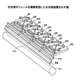
次に、図3を用いて光走査装置の概要について説明する。光走査装置は、複数の光走査モジュール203が像担保体である感光体の長軸方向に隣接して配置される、この図では単一感光体に対して4器の光走査モジュール203が配設されている。各光走査モジュール203は感光体面上を分割して任意の範囲を光走査可能である。
Next, an outline of the optical scanning device will be described with reference to FIG. In the optical scanning device, a plurality of
この光走査装置では、上述したように、複数レーザー光源200から出射された光ビームは、偏向ミラー40により偏向され、感光体の長軸方向である主走査方向に走査される。なお、複数レーザー光源200は、本実施の形態において、複数の光ビームであり、2本光ビームを用いている。
In this optical scanning device, as described above, the light beams emitted from the plurality of laser
2本の光ビームのうちの一本の走査光路上には、等角走査を等速走査への変換用fθレンズ207,208、光路変更ミラー209が配設され、感光体面上211に微小レーザービームスポット212を結像する。他方のビームの走査光路上には光検知モジュール216が配設され、偏向ミラー40により偏向されたビームが光検知モジュール216の長軸方向に走査される。
On one scanning optical path of the two light beams,
このように、本実施の形態における光走査装置では、単一光検知モジュール216に対して配設された四つの光走査モジュール203から偏向された光ビームは光検知モジュール216面上を分割して任意の範囲を光走査可能となっている。
Thus, in the optical scanning device according to the present embodiment, the light beams deflected from the four
また、光検知モジュール216は光検知部材217が等間隔で配置され、光を検知する光量に対応した光電流を発生する。隣接する光ビームが同時に光検知部材を走査した時光量は通常の量より多い光量を受け、光電流もそれに見合って多くなる。
In the
このときの重複検知信号について説明する。図4は複数の光走査モジュールが隣接配設された光走査装置を示しており、光ビーム走査領域が隣接する境界部で重複している例が示されている。 The overlap detection signal at this time will be described. FIG. 4 shows an optical scanning device in which a plurality of optical scanning modules are arranged adjacent to each other, and shows an example in which light beam scanning regions overlap at adjacent boundary portions.
図4において、左側から2器の隣接する光走査モジュールの光検知モジュール216面上での走査領域は、それぞれ左から、WA,WBであり、走査領域における重複領域はWOABである。LA、LBは、各光走査モジュールの揺動振幅である。LOABは、揺動振幅で重複する領域である。
In FIG. 4, the scanning areas on the surface of the
光検知モジュール216を拡大したものを、図5を用いて説明する。図5には、さらに、検知信号例C、重複検知信号例Dも示している。また、図5には、光ビームが光検知モジュールを光走査した時の光検知信号が図示されている。また、光検知モジュール216内の光検知部材217を拡大したものも図示されている。
An enlarged view of the
この図5において、WA、WB、WC、WDは、図4と同様に、4器の光走査モジュールが光走査する領域を示している。また、WOA、WOB、WOCも同様に、2つの光走査モジュールが光走査する重複領域である。また、Pa*は、領域WAで検地された信号を表し、ta*は、領域WAにおける検知信号間の走査時間を表している。Pb*、tb*も同様である。Pab*は、領域WOAで検知された重複信号である。 In FIG. 5, WA, WB, WC, and WD indicate areas in which four optical scanning modules perform optical scanning, as in FIG. Similarly, WOA, WOB, and WOC are overlapping regions where two optical scanning modules perform optical scanning. Pa * represents a signal detected in the area WA, and ta * represents a scanning time between detection signals in the area WA. The same applies to Pb * and tb *. Pab * is a duplicate signal detected in the area WOA.
図5では、光検知部材217が一定間隔で配置され、隣接する互いの重複範囲WOABには、光検知部材217が3個配置されている。
In FIG. 5, the
走査領域WAで走査することによる検知信号はPan-2,Pan-1,Panであり、走査領域WBで走査することによる検知信号はPb1、Pb2、Pb3である。 Detection signals obtained by scanning in the scanning area WA are Pan-2, Pan-1, Pan, and detection signals obtained by scanning in the scanning area WB are Pb1, Pb2, and Pb3.
このとき、走査領域WAでの走査時間Pan-2〜Pan-1の時間△ta1、Pan-1〜Panの時間△ta2とし、走査領域WBでの走査時間Pb1〜Pb2の時間△tb1、Pb2〜Pb3の時間△tb2とする。 At this time, time Δta1 of scanning time Pan-2 to Pan-1 and time Δta2 of Pan-1 to Pan-1 in scanning area WA, and time Δtb1, Pb2 of scanning time Pb1 to Pb2 in scanning area WB Let Pb3 be the time Δtb2.
そして、走査時間△ta1と△tb1の比較と、走査時間△ta2と△tb2の比較を行うことにより、走査速度の差分及びお互いの位相を知る事が出来る。この差分及び位相が隣接する光走査モジュールの継ぎ目の調整に用いる事により、選り正確に調整が可能となる。 Then, by comparing the scanning times Δta1 and Δtb1 and comparing the scanning times Δta2 and Δtb2, the difference in scanning speed and the phase of each other can be known. By using this difference and phase for adjusting the joints of adjacent optical scanning modules, selection and adjustment can be made accurately.
次に、光走査モジュール203が光検知モジュール216を光走査する時の信号発生の概略を、図6を用いて説明する。
Next, an outline of signal generation when the
図6のグラフAは、偏向ミラーの振幅を示すものである。このように、偏向ミラーが位置検知センサL1の位置から位置検知センサLnの位置の間隔の振幅で揺動しているとすると、振幅間に配設された光検知部材217で光を受光すると、光検知部材の位置に対応した信号を発生する。
Graph A in FIG. 6 shows the amplitude of the deflection mirror. As described above, when the deflection mirror swings with the amplitude of the interval between the position detection sensor L1 and the position detection sensor Ln, when the
このとき、光検知部材の位置をそれぞれL1, L2, L3..... Lnとすると、図6のグラフBに示す様、位置検知信号P1,P2,P3....Pnが出力される。また、図6の例ではL1〜Lnの範囲で揺動しているので、グラフCに示されるように、L1を、揺動周期Taを計測する同期基準信号とする。また、グラフDに示されるように、L1は、偏向ミラーを揺動する揺動力を与える駆動信号印加タイミングを調整する信号としても用いられる。 At this time, assuming that the positions of the light detection members are L1, L2, L3,... Ln, position detection signals P1, P2, P3,. . Further, in the example of FIG. 6, since the rocking is in the range of L1 to Ln, as shown in the graph C, L1 is set as a synchronization reference signal for measuring the rocking cycle Ta. Further, as shown in the graph D, L1 is also used as a signal for adjusting the drive signal application timing for applying a swinging force that swings the deflection mirror.
揺動振幅が検知位置L1〜Lnの幅の場合、この揺動振幅は揺動条件により変動する場合がある。例えば揺動振幅が検知位置L2〜Ln-1の間であった場合、検知位置L2で検知された同期検知信号が同期基準信号と見なされ、この信号を基準にして揺動周期の計測、また、偏向ミラーを揺動する揺動力を与える駆動信号印加タイミングを調整する信号としても用いることが出来る。 When the swing amplitude is the width of the detection positions L1 to Ln, the swing amplitude may vary depending on the swing condition. For example, when the swing amplitude is between the detection positions L2 to Ln-1, the synchronization detection signal detected at the detection position L2 is regarded as a synchronization reference signal, and the swing cycle is measured based on this signal. Also, it can be used as a signal for adjusting the drive signal application timing for applying a swinging force to swing the deflection mirror.
この様に複数の光検知部材を一定間隔で配置することにより、揺動振幅が変動(小さくなっても)しても、偏向ミラーの揺動軌跡を検知出来る。 By arranging a plurality of light detection members at regular intervals in this way, the swing locus of the deflection mirror can be detected even if the swing amplitude varies (even if it becomes smaller).
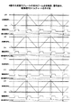
以上説明した図6の光走査モジュールと光検知モジュールの関係を述べたが、光走査モジュールを複数個配設して用いる構成での軌跡について図7で示している。 The relationship between the optical scanning module and the optical detection module in FIG. 6 described above has been described. FIG. 7 shows the trajectory in a configuration in which a plurality of optical scanning modules are arranged and used.
図7では、光走査装置に設けられた4器の光走査モジュールをそれぞれ光走査モジュールA,B,C,Dとおき、それらの軌跡が描かれている。これらの軌跡は、各光走査モジュールA,B,C,Dの揺動振幅が、それぞれLA1〜LAn、LB1〜LBn、LC1〜LCn、LD1〜LDnであり、揺動周期はそれぞれTA,TB,TC,TDであるので、これら振幅と周期である揺動軌跡となっている。 In FIG. 7, four optical scanning modules provided in the optical scanning device are respectively set as optical scanning modules A, B, C, and D, and their trajectories are drawn. In these trajectories, the oscillation amplitudes of the optical scanning modules A, B, C, and D are LA1 to LAn, LB1 to LBn, LC1 to LCn, and LD1 to LDn, respectively, and the oscillation periods are TA, TB, Since these are TC and TD, the swing locus is the amplitude and the period.
4器の光走査モジュールより構成された光走査装置を画像形成行う光書込み装置として用いる場合、4器の光走査モジュールの揺動軌跡の揺動周期、揺動振幅が同一でないと形成される画像品質が劣化する事が懸念される。 When an optical scanning device composed of four optical scanning modules is used as an optical writing device for forming an image, an image formed when the oscillation period and oscillation amplitude of the oscillation trajectories of the four optical scanning modules are not the same. There is concern that the quality will deteriorate.
このような揺動軌跡が異なる場合について、図8を用いて説明する。図8は、走査周期A軌跡と走査周期B軌跡の走査周期が異なる例を示している。図8において、X軸と平行な直線は、光検知位置を示している。また、PA2〜PAn-1、PB2〜PBn-1は、走査周期A軌跡と走査周期B軌跡でのL2〜Lnで検知した信号を示しており、TA、TBはそれぞれ周期の周期である。 A case where the swing trajectories are different will be described with reference to FIG. FIG. 8 shows an example in which the scanning cycle of the scanning cycle A and the scanning cycle B is different. In FIG. 8, a straight line parallel to the X-axis indicates the light detection position. PA2 to PAn-1 and PB2 to PBn-1 indicate signals detected from L2 to Ln in the scanning cycle A locus and the scanning cycle B locus, respectively, and TA and TB are cycle periods.
この図8に示されるように、走査周期が異なると、図中検知信号PA2,PB2の検知タイミングが異なり、例えば、それぞれPA、PBを基準同期信号とした場合、画像形成時のタイミング、偏向ミラーの揺動力印加タイミングも異なり、隣接する光走査モジュールの継ぎ目が乱れることになる。 As shown in FIG. 8, when the scanning cycle is different, the detection timings of the detection signals PA2 and PB2 in the drawing are different. For example, when PA and PB are used as the reference synchronization signals, respectively, the timing at the time of image formation, the deflection mirror The swinging force application timings are also different, and the joints between adjacent optical scanning modules are disturbed.
このように、複数の光走査モジュールを用いた場合、各光走査モジュールの揺動周期或は揺動振幅等が偏向ミラーの経時変化、揺動力を与える電圧の変化、温度湿度気圧等の環境の変化により微妙に変動する事が知られている。このような変動は適時調整可能とし常に適正な揺動周期及び揺動振幅の設定値が設定可能であれば良い。その解決法として、主走査方向に配設された光検知モジュールから得られる光検知信号を用いて前記揺動周期及び揺動振幅の設定値が設定可能出来る。 As described above, when a plurality of optical scanning modules are used, the oscillation period or oscillation amplitude of each optical scanning module changes with time in the deflection mirror, the voltage applied to the oscillation force, the temperature, humidity, and atmospheric pressure. It is known to change slightly with changes. It is only necessary that such fluctuations can be adjusted in a timely manner, and an appropriate set value of the oscillation cycle and oscillation amplitude can always be set. As a solution to this, the set values of the oscillation period and oscillation amplitude can be set using a light detection signal obtained from a light detection module arranged in the main scanning direction.
光走査装置(図3参照)では、感光体面上のビームスポットは常に所定位置に結像しなければならない。一般的に隣り合う結像点間の位置誤差は12.5%以下の精度が要求されている。 In the optical scanning device (see FIG. 3), the beam spot on the surface of the photosensitive member must always form an image at a predetermined position. In general, the positional error between adjacent imaging points is required to have an accuracy of 12.5% or less.
このような書き込み装置に用いる光走査装置での、走査位置精度維持の方法について、先ほど説明した図6を用いて説明する。偏向ミラーに因る揺動軌跡が理想波形を描いた場合、揺動軌跡波形は図6のグラフAに示される単振動波形を示す。また、感光体面上にビームスポットを形成する範囲は感光体面上の長軸方向走査領域である。 A method of maintaining the scanning position accuracy in the optical scanning device used for such a writing device will be described with reference to FIG. When the swing trajectory caused by the deflecting mirror draws an ideal waveform, the swing trajectory waveform shows a simple vibration waveform shown in graph A of FIG. Further, the range in which the beam spot is formed on the photoreceptor surface is the long axis direction scanning region on the photoreceptor surface.
この感光体と並行に光検知モジュールが配設され、4器配列された各光走査モジュールの偏向ミラーで偏向された光ビームを検知する光検知モジュールが配され、これらで検知された信号P1〜Pnが得られる。 A photodetection module is arranged in parallel with the photoconductor, and a photodetection module for detecting the light beam deflected by the deflection mirror of each of the four optical scanning modules arranged is arranged. Signals P1 to P1 detected by these are detected. Pn is obtained.
信号P1〜Pnから、グラフCに示すような同期基準信号P1が生成される。同期基準信号P1を基準として、他の信号P2〜PnではP1から各信号間の時間が計測される。 A synchronization reference signal P1 as shown in the graph C is generated from the signals P1 to Pn. With respect to the synchronization reference signal P1, the other signals P2 to Pn measure the time between each signal from P1.
上述した図5では、信号Pa1とPa2間の時間Ta1,信号Pa1とPa3間の時間Ta2、.... 信号P1とPn間時間Tanが示されている。この各時間Ta1,Ta2,.....Tanを計測することにより、偏向ミラーに因る揺動軌跡の周期変動を計測する事が出来、計測結果から変動量を求め補正設定量が定まり、補正制御が可能になる。 In FIG. 5 described above, time Ta1 between signals Pa1 and Pa2, time Ta2 between signals Pa1 and Pa3,... Time Tan between signals P1 and Pn are shown. By measuring each time Ta1, Ta2, ... Tan, it is possible to measure the periodic fluctuation of the swinging locus caused by the deflecting mirror, and the amount of fluctuation is obtained from the measurement result, and the correction setting amount is determined. Correction control becomes possible.
このように、走査領域の光ビーム軌跡の計測可能とする感光体面上走査領域の範囲に、光検知部材を配置した構成の光走査装置を提供することができる。 As described above, it is possible to provide an optical scanning device having a configuration in which the light detection member is arranged in the range of the on-photosensitive-surface scanning region where the light beam trajectory of the scanning region can be measured.
次に、複数光走査モジュールの偏向ミラー揺動制御に関して説明する。走査時間を測定する測定手段と、偏向ミラーの揺動周期を調整する調整量を設定する調整量設定手段と、偏向ミラーの揺動周期を調整する調整手段は各モジュールに備えられ、各モジュールは独立して偏向ミラーの揺動周期をコントロールする事が出来る。 Next, the deflection mirror swing control of the multiple light scanning module will be described. Each module includes a measuring means for measuring the scanning time, an adjustment amount setting means for setting an adjustment amount for adjusting the swinging period of the deflecting mirror, and an adjusting means for adjusting the swinging period of the deflecting mirror. The oscillation cycle of the deflecting mirror can be controlled independently.
この例として、図9の光走査装置の制御ブロック図について説明する。図9には、記憶手段に対応するRAM33と、ROM32と、MPU31と、クロック30と、アドレス/データバス34と、駆動信号発生タイミング制御部36と、駆動信号発生器39と、電圧可変部47と、ドライバーアンプ部41と、光ビーム発生タイミング制御部50と、光ビームドライブ部52と、光ビーム発生部51と、複数レーザー光源200と、光検知モジュール216と、感光体211と、センサアンプ部42と、位置信号検出部38と、基準クロック生成部48と、時間計測部49と、同期信号生成部37と、時間差演算回路46とが示されている。
As an example of this, a control block diagram of the optical scanning device in FIG. 9 will be described. In FIG. 9, a RAM 33, a
このうち、駆動信号発生タイミング制御部36と、駆動信号発生器39と、電圧可変手段47と、ドライバーアンプ部41から構成される駆動部が、偏向ミラー40を揺動可能とし、其々の光走査モジュールに配設されている。この駆動部は、偏向ミラー駆動手段に対応する。
Among these, the drive unit composed of the drive signal generation timing control unit 36, the
光検知モジュールの光検知部材に対応した複数のセンサアンプ部42、位置検知信号生成部38、同期基準信号生成部37、時間差演算回路部46は検知手段であり、この検知手段により、信号検知部からの信号が検知及び格納される。
The plurality of
駆動部はMPU31からの制御指示に従い、電圧可変部47では電極に印加する電圧を設定し、デジタルデータ格納部36には電極に印可する信号の駆動周波数に関するデータが格納させ、駆動信号生成器39ではデジタルデータ格納部36に格納されたデータに対応した駆動周波数を生成する。
In accordance with a control instruction from the
駆動信号生成器39で生成された信号はドライバーアンプ部41に接続されている。ドライバーアンプ部41では信号印加電圧が電圧可変部47により任意に可変可能となっている。ドライバーアンプ部41の出力は偏向ミラーに配設された端子に接続され各電極に信号を与える。
The signal generated by the
検知手段では、センサアンプ部42が光検知モジュール216の信号検知部から取り出した信号を増幅し、位置検知信号生成部38が位置検知信号を生成し、その位置検知信号から同期基準信号生成部37が同期基準信号を生成する。
In the detection means, the
また基準クロック生成部48は同期基準信号に同期したクロックを生成し、各同期基準信号間の時間を計測するために利用される。
The
光ビーム発生部は、光ビーム発生タイミング制御部50と、光ビーム発生部51と、光ビームドライブ部52から構成される。光ビーム発生部は、感光体面上への光ビーム走査制御、及び光検知モジュールへの光ビーム走査制御を行う。
The light beam generation unit includes a light beam generation
RAM33は調整手段が調整する調整量を記憶可能としている、一度調整量をRAM33に記憶した後は、記憶した調整量に基づいて調整処理を実行することにより、毎時調整量を算出する手順が省略可能となり、より早い調整処理時間で実行可能となる。 The RAM 33 can store the adjustment amount adjusted by the adjustment means. Once the adjustment amount is stored in the RAM 33, the adjustment process is executed based on the stored adjustment amount, thereby omitting the procedure for calculating the hourly adjustment amount. This becomes possible and can be executed with a faster adjustment processing time.
以上説明した構成で、複数の光走査モジュールは感光体面上に画像を形成するには、お互いに揺動周期、位相が同一で有る事が要求される。先ほど説明した図7に示されるように、全て同一の揺動軌跡で揺動する必要がある。 With the configuration described above, a plurality of optical scanning modules are required to have the same oscillation cycle and phase in order to form an image on the surface of the photoreceptor. As shown in FIG. 7 described above, it is necessary to swing all along the same swinging locus.
各光走査モジュールを同一揺動軌跡で揺動させるために、例えば起動開始時などの所定のタイミングを定めた場合、そのタイミングで先ず任意の一つの光走査モジュールを揺動動作させ、その後他の残りを順次揺動させる手順とする。 In order to swing each optical scanning module with the same swinging locus, for example, when a predetermined timing such as at the start of activation is determined, any one optical scanning module is first swung at that timing, and then the other scanning modules are The procedure is to swing the rest sequentially.
この方法から、任意の1つの光走査モジュールの光走査揺動軌跡から得られた設定量を基準設定量とし、この基準設定量を基に全ての駆動部に可動ミラー揺動力を与えることとする事により、各々独立して各光走査モジュールに毎時同一揺動設定量を与える方法に比べ、揺動時の環境条件に沿った設定量を毎回調整する事が出来る為、起動開始時の起動手順が簡便に行える。 From this method, the set amount obtained from the optical scanning swing locus of any one optical scanning module is used as the reference set amount, and the movable mirror swing force is applied to all the drive units based on this reference set amount. As a result, it is possible to adjust the set amount according to the environmental conditions at the time of oscillation compared to the method in which each optical scanning module is independently given the same oscillation setting amount every hour. Can be done easily.
さらに、先ほどの起動開始時の起動手順において、任意の1つの光走査モジュールの光走査に起因する設定量を基準設定量とする光走査モジュールを、主走査領域の開始位置に配置される光走査モジュールとすることにより、光走査方向の上流から下流に向けて順次設定可能とする事となり、起動開始時の起動手順がより簡便に行える。 Further, in the startup procedure at the start of startup, the optical scanning module in which the optical scanning module with the set amount resulting from the optical scanning of any one optical scanning module as the reference set amount is arranged at the start position of the main scanning region. By using a module, it is possible to sequentially set from upstream to downstream in the optical scanning direction, and the startup procedure at the start of startup can be performed more easily.
さらに、任意の1つの光走査モジュールの光走査に起因する設定量を基準設定量とし、他の各光走査モジュールでの走査による設定量は、前記基準設定量との比較量となし、基準設定量と各々比較量との差分を補正する補正設定量として各々の駆動部に可動ミラー揺動力を与えることにより各光走査モジュール間の微妙な揺動周期の調整が可能となる。 Further, the set amount resulting from the optical scanning of any one optical scanning module is used as the reference set amount, and the set amount by scanning in each of the other optical scanning modules is the comparison amount with the reference set amount, the reference set amount By applying a movable mirror swinging force to each drive unit as a correction set amount for correcting the difference between the amount and each comparison amount, it is possible to finely adjust the swing cycle between the optical scanning modules.
次に、図10を用いて偏向ミラーについて説明する。偏向ミラーはシリコンマイクロマシニング技術を用いて形成されている。 Next, the deflection mirror will be described with reference to FIG. The deflection mirror is formed using silicon micromachining technology.
この偏向ミラーは、シリコン基板1と、支持部材2と、固定電極3と、可動部材配設電極4と、ミラー部9と、可動部材10とで構成される。
The deflecting mirror includes a
シリコン基板1は、矩形の単層厚板で形成される。可動部材10は、可動部材配設電極4とミラー部9が形成されている。可動部材配設電極4に対向して固定電極3と可動部材10に一体的に両側に突出形成された支持部材2は、両端でシリコン基板に固定されている。これにより、前記可動部材10は支持部材2の捩じりにより、ミラー部9の平面方向と垂直な方向に揺動可能となる。
The
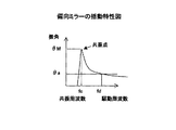
このように、偏向ミラーを配設した可動部材と、前記可動部材を揺動可能に支持する支持部材とを有し、可動部材を揺動可能とする光走査装置において、通常駆動周波数は、可動部材の持つ固有振動数に共振する共振周波数とする事が多い。 As described above, in the optical scanning device having the movable member provided with the deflection mirror and the support member that supports the movable member so as to be swingable, the normal drive frequency is movable. In many cases, the resonance frequency resonates with the natural frequency of the member.
これは、共振周波数点では可動部材の揺動角が最大になる為である。図11は、偏向ミラーの揺動特性図である。この図11の揺動特性図において、可動部材の持つ固有振動数に共振する共振周波数領域は狭く、Q値が高い駆動物体となっている。従来はQ値が高い為光ビームの偏向角を正確に検知する為、高精度のセンサを多数設置する必要があったり、検知回路が複雑になり製造コストも増大する問題があった。 This is because the swing angle of the movable member is maximized at the resonance frequency point. FIG. 11 is a swing characteristic diagram of the deflection mirror. In the oscillation characteristic diagram of FIG. 11, the resonance frequency region resonating with the natural frequency of the movable member is narrow, and the driving object has a high Q value. Conventionally, since the Q value is high, in order to accurately detect the deflection angle of the light beam, it is necessary to install a large number of high-precision sensors, and the detection circuit becomes complicated and the manufacturing cost increases.
本実施の形態で用いる駆動周波数は図11において共振周波数から外れた周波数を用いて可動部材を駆動する方式である。このようにQ値が低い周波数を用いる事により、周波数が変動対するミラー揺動角の変動が少ない、即ちミラー駆動周波数を変化させてもミラー揺動角の変動が少なくなる。 The drive frequency used in the present embodiment is a method of driving the movable member using a frequency deviating from the resonance frequency in FIG. By using a frequency having a low Q factor in this way, the fluctuation of the mirror swing angle with respect to the fluctuation of the frequency is small, that is, the fluctuation of the mirror swing angle is reduced even if the mirror drive frequency is changed.
従ってミラー揺動特性のジター等の発生を減少させるコントロールが容易になり、また複数ミラーを用いた場合複数ミラーでの駆動周波数を一致し易い。また、駆動パルスを印加するためのミラーの揺動位置を検知する方法も簡便化可能となる。 Therefore, it becomes easy to control to reduce the occurrence of jitter of the mirror swing characteristic, and when a plurality of mirrors are used, the driving frequencies of the plurality of mirrors are easily matched. Further, it is possible to simplify the method for detecting the swing position of the mirror for applying the drive pulse.
次に、図12を用いて、上述した書き込み手段を用いた画像形成装置について説明する。図12には、帯電部304と、光書き込み部303と、現像部302と、転写部309と、感光体305と、クリーニング部306と、定着部307と、用紙搬送部308と、用紙収納部300と、給紙部301と、ローラ310と、レジスト部311とが示されている。
Next, an image forming apparatus using the above-described writing unit will be described with reference to FIG. In FIG. 12, the charging
この画像形成装置には、感光体305の廻りに帯電部304と、光書き込み部303と、現像部302と、転写部309と、クリーニング部306とが配される。図示されていない画像形成装置制御部により画像形成の開始を指示されると、感光体305は時計方向に回転して、光書き込み部303は、偏向ミラーを駆動し同期信号を生成し、帯電部304により感光体を帯電する。そして、光書き込み部303にて図示していない外部入力装置から入力された画像データに対応した潜像が形成され、現像部302にて像可視化剤により可視化像を得る。
In this image forming apparatus, a charging
用紙収納部300に収納された用紙は、給紙部301により給紙され、レジスト部311により用紙搬送タイミングと書き込みタイミングを合わせ所定の位置に像可視化剤による顕在像を転写部309にて転写可能とする。
The paper stored in the
用紙に転写された像可視化剤による顕在像は定着部307で定着され、入力された画像データが用紙上に可視化固定される。光書込み部303は、今まで説明した光走査装置を搭載している。
The actual image transferred by the image visualization agent transferred to the paper is fixed by the fixing
光走査装置は外部入力装置から画像データが入力されないアイドル状態で適時光走査装置の偏向ミラーの揺動動作状態を調査できる。図示されていない手段で偏向ミラーを、位置検知信号を検知する光ビーム走査である位置検知光ビーム走査モードに設定する。光ビームを発生し位置検知部材を走査させ、位置検知信号P1〜Pnを得、これらを基に、同期基準信号Pa1,Pb1,Pc1,Pd1,基準クロック、各位置検知信号間の時間等をデータ信号処理部で演算しRAMに格納する。 The optical scanning device can investigate the oscillating operation state of the deflection mirror of the optical scanning device in a timely manner in an idle state where no image data is input from the external input device. The deflection mirror is set to a position detection light beam scanning mode which is a light beam scanning for detecting a position detection signal by means not shown. Light beam is generated and the position detection member is scanned to obtain position detection signals P1 to Pn. Based on these signals, synchronization reference signals Pa1, Pb1, Pc1, Pd1, reference clock, time between each position detection signal, etc. It is calculated by the signal processing unit and stored in the RAM.
次に揺動軌跡の理想波形から算出された予め記憶部に記憶されている上記、位置検知信号P1〜Pn、同期基準信号Pa1,Pb1,Pc1,Pd1,基準クロック、各位置検知信号間の時間、等の標準値と前記計測により得られた値とを比較演算し、標準値との差分求める。その差分を元に周期を演算しRAMに記憶する。 Next, the position detection signals P1 to Pn, the synchronization reference signals Pa1, Pb1, Pc1, Pd1, the reference clock, and the time between the position detection signals stored in advance in the storage unit calculated from the ideal waveform of the swing locus. , Etc. and the value obtained by the measurement are compared, and a difference from the standard value is obtained. The period is calculated based on the difference and stored in the RAM.
次に、外部入力装置から画像データが入力され感光体面上にビームスポットを形成するモードについて述べる。外部からの画像データ入力を受けて、データ信号処理部は画像データに対応したビームスポットを感光体面上に形成する。 Next, a mode in which image data is input from an external input device and a beam spot is formed on the surface of the photoreceptor will be described. Upon receiving image data input from the outside, the data signal processing unit forms a beam spot corresponding to the image data on the photosensitive member surface.
先ず始めに、図示されていない手段で偏向ミラーを、感光体面上を光ビーム走査する感光対面上光ビーム走査モードに設定する。次に偏向ミラーを揺動駆動し、一ライン毎感光体面上にビームスポットを形成していく。 First, the deflection mirror is set to a light beam scanning mode on the photosensitive surface that scans the surface of the photosensitive member by means not shown. Next, the deflection mirror is driven to swing, and a beam spot is formed on the surface of the photoreceptor for each line.
光ビームは光検知モジュール(図3参照)で得られる信号を検知感光体面上へのビームスポット形成の基準位置とする。光検知モジュールの走査タイミングは、外部からの画像データが入力していない状態や、記録用紙への印刷ジョブのジョブ間で行う場合である。光検知モジュールは、複数の光ビームを同時に発光可能な事より、位置検知信号を検知する光ビーム走査である位置検知光ビーム走査モードと感光体面上にビームスポットを形成するモードを同時に行うことが出来、偏向ミラー揺動軌跡の情報が逐次入手でき、より精度の良い制御が可能となる。 For the light beam, a signal obtained by the light detection module (see FIG. 3) is used as a reference position for forming a beam spot on the detection photoconductor surface. The scanning timing of the light detection module is in a state where image data from the outside is not input, or when it is performed between jobs of a print job on a recording sheet. Since the light detection module can emit a plurality of light beams at the same time, it can simultaneously perform a position detection light beam scanning mode that is a light beam scanning for detecting a position detection signal and a mode for forming a beam spot on the surface of the photosensitive member. The deflection mirror swing trajectory information can be obtained sequentially, and more accurate control is possible.
以上説明したように本実施の形態では、複数配置された光走査モジュールの揺動軌跡の周波数、位相を計測する事が出来、各複数光走査モジュールの周波数、位相を管理可能とし、各光走査モジュール間の継ぎ目のずれを減少する事が可能となる。 As described above, in the present embodiment, the frequency and phase of the oscillation trajectory of a plurality of optical scanning modules can be measured, and the frequency and phase of each of the plurality of optical scanning modules can be managed. It is possible to reduce the seam shift between modules.
また、本実施の形態では、光走査モジュールの揺動幅(振幅)が変動して任意の振幅時の揺動周期が計測可能である。そして同様に振幅が変動しても任意の位置を光書出し位置の同期検知手段として計測可能とする事により継ぎ目のずれ少ない制御が可能になる。 Further, in this embodiment, the oscillation width (amplitude) of the optical scanning module varies, and the oscillation cycle at an arbitrary amplitude can be measured. Similarly, even if the amplitude fluctuates, it is possible to perform control with less seam deviation by making it possible to measure an arbitrary position as the optical writing position synchronization detecting means.
さらに、本実施の形態では、必要とされる任意の光走査モジュールの揺動周期及び、光書出し位置の計測可能とする事により光走査モジュールの加減時の制御が容易になる。 Furthermore, in the present embodiment, it becomes possible to easily control the optical scanning module when adjusting the optical scanning module by making it possible to measure the required oscillation period of the optical scanning module and the optical writing position.
また、本実施の形態では、隣接する光走査モジュールの揺動周期及び、光書出し位置の計測値を直接比較する事が出来、より正確に隣接する光走査モジュール間の調整が可能となる。 In this embodiment, the oscillation period of adjacent optical scanning modules and the measured value of the optical writing position can be directly compared, and adjustment between adjacent optical scanning modules can be performed more accurately.
また、本実施の形態では、光検知モジュールから得られた位置検知信号間を通過する時間を計測出来、さらに位置検知信号間を通過する基準時間を設定しておく事に居り、基準時間との比較が可能となり、基準時間に対する差異を求める事ができる。また、差異に基づき差異を調整する様調整量を設定する調整量設定手段に調整され、揺動周期調整手段より、偏向ミラーの揺動周期を調整し、各光走査モジュールの光走査周期を同一にする事が出来る。 Further, in this embodiment, it is possible to measure the time passing between the position detection signals obtained from the light detection module, and further to set a reference time for passing between the position detection signals. Comparison is possible, and the difference with respect to the reference time can be obtained. Further, the adjustment amount is set by an adjustment amount setting means for setting an adjustment amount so as to adjust the difference based on the difference, and the swing period of the deflection mirror is adjusted by the swing period adjustment means so that the optical scanning period of each optical scanning module is the same. Can be made.
さらに、本実施の形態では、複数光走査装置の配置数の増減に伴っても各光走査モジュール単独で各処理を行う事が出来、光走査装置の構成が簡単になる。 Furthermore, in this embodiment, each process can be performed by each optical scanning module independently even when the number of arrangements of the plurality of optical scanning devices is increased or decreased, and the configuration of the optical scanning device is simplified.
また、本実施の形態では、1つの光走査モジュールの光走査揺動軌跡から得られた設定量を基準設定量とし、この設定量を基に全ての偏向ミラー駆動手段に偏向ミラー揺動力を与えることとする事により、各々独立して各光走査モジュールに毎時同一揺動設定量を与える方法に比し、揺動時の環境条件に沿った設定量を毎回調整する事が出来る為、起動開始時の起動手順が簡便に行える。 In this embodiment, the set amount obtained from the optical scanning swing locus of one optical scanning module is used as a reference set amount, and the deflection mirror swinging force is applied to all the deflecting mirror driving means based on this set amount. By doing so, it is possible to adjust the set amount according to the environmental conditions at the time of swinging, compared to the method of giving the same swinging set amount per hour to each optical scanning module independently, so start-up is started. The starting procedure at the time can be done easily.
さらに、本実施の形態では、基準設定量を定める光走査モジュールは主走査領域の開始位置に配置される光走査モジュールとすることにより、光走査方向の上流から下流に向けて順次設定可能とする事により、起動開始時の起動手順がより簡便に行える。 Furthermore, in this embodiment, the optical scanning module that determines the reference set amount is an optical scanning module that is arranged at the start position of the main scanning region, so that it can be set sequentially from upstream to downstream in the optical scanning direction. As a result, the startup procedure at the start of startup can be performed more easily.
さらに、本実施の形態では、モジュール走査による設定量を、基準設定量と各々比較量との差分を補正する補正設定量として各々の偏向ミラー駆動手段に偏向ミラー揺動力を与えることにより各光走査モジュール間の微妙な揺動周期の調整が可能となる。 Furthermore, in this embodiment, each optical scanning is performed by applying a deflection mirror swinging force to each deflecting mirror driving means as a set amount for correcting the difference between the reference set amount and each comparison amount. It is possible to finely adjust the oscillation cycle between modules.
また、本実施の形態では、調整量をRAMに記憶した後は、記憶した調整量に基づいて上記調整処理を実行することに因り、毎時調整量を算出する手順が省略可能となりより早い調整処理時間で実行可能となる。 Further, in the present embodiment, after the adjustment amount is stored in the RAM, the procedure for calculating the hourly adjustment amount can be omitted because the adjustment processing is executed based on the stored adjustment amount, and the faster adjustment processing It can be executed in time.
また、本実施の形態では、所望する偏向ミラーの揺動角度を、可動部材の持つ固有振動数に共振する共振周波数を除いた周波数領域で実現することより、経時変化、温度変化に強い、或は変動を容易に修正可能とする駆動制御方式が選択でき、より安定した光走査装置が提供できる。 Further, in the present embodiment, by realizing the desired swing angle of the deflecting mirror in the frequency region excluding the resonance frequency that resonates with the natural frequency of the movable member, it is resistant to changes with time and temperature, or Can select a drive control system that can easily correct fluctuations, and can provide a more stable optical scanning device.
さらに、本実施の形態では、上述した光走査装置を画像形成装置に用いることにより、従来のポリゴンミラーを用いた光走査装置で画像形成する画像形成装置より、走査幅の広い、高速な画像形成装置となる。 Furthermore, in the present embodiment, by using the above-described optical scanning device for an image forming apparatus, a high-speed image formation with a wider scanning width than an image forming apparatus that forms an image with a conventional optical scanning apparatus using a polygon mirror. It becomes a device.
1 シリコン基板
2 支持部材
3 固定電極
4 可動部材配設電極
9 ミラー部
10 可動部材
30 クロック
31 MPU
32 ROM
33 RAM
34 アドレス/データバス
36 駆動信号発生タイミング制御
37 同期基準信号
38 位置検知信号生成部
39 駆動信号生成器
40 偏向ミラー
41 ドライバーアンプ部
42 センサアンプ部
44 光ビーム発生部
50 光ビーム発生タイミング制御
51 光ビーム発生部
52 光ビームドライブ部
101 基板
102 ミラー
103 トーションバー
104、108 パッド
105 ミラー電極部
106 絶縁体
107 固定電極
200 複数レーザー光源
201 光ビームa
202 光ビームb
203 光走査モジュール
207、208 fθレンズ
209 折り返しミラー
211 感光体
212 結像スポット列
216 光検知モジュール
217 光検知部材
300 用紙収納部
301 用紙給紙部
302 現像部
303 複数ビーム書き込み部
304 帯電部
305 感光体
306 クリーニング部
307 定着部
308 用紙搬送部
DESCRIPTION OF
32 ROM
33 RAM
34 Address / Data Bus 36 Drive Signal
202 Light beam b
203
Claims (14)
前記光走査モジュールからの光ビームを検知し、光検知信号を出力する光検知モジュールとを有し、
前記光走査モジュールを主走査方向に走査ラインが一直線になるように複数器配列したことを特徴とする光走査装置。 An optical scanning module for emitting a light beam;
A light detection module that detects a light beam from the light scanning module and outputs a light detection signal;
An optical scanning apparatus comprising a plurality of the optical scanning modules arranged so that scanning lines are aligned in the main scanning direction.
光ビームを発する光源手段と、
前記光ビームを偏向走査する偏向ミラーと、
前記偏向ミラーを揺動する偏向ミラー駆動手段と
を有することを特徴とする請求項1に記載の光走査装置。 The light detection module includes:
Light source means for emitting a light beam;
A deflection mirror that deflects and scans the light beam;
The optical scanning device according to claim 1, further comprising: a deflecting mirror driving unit that swings the deflecting mirror.
複数の光ビームを発し、該複数ビームの一つは前記光検知モジュール面を走査するビームであり、
他のビームは画像信号により独立に変調されるとともに、像担保体の被走査面上に光書込みを行う光ビームであることを特徴とする請求項2記載の光走査装置。 The light source means includes
Emitting a plurality of light beams, one of the plurality of beams is a beam scanning the surface of the light detection module;
3. The optical scanning device according to claim 2, wherein the other beam is a light beam that is independently modulated by an image signal and that performs optical writing on a surface to be scanned of the image security body.
等間隔で配列され光検知部材を含み、
前記光検知部材により、光ビームが所定の位置を通過したことを検出して位置検知信号を出力するとともに、光書出し位置を検出して同期検知信号を出力することを特徴とする請求項2または3に記載の光走査装置。 The light detection module includes:
Including light detection members arranged at equal intervals,
3. The light detection member detects that a light beam has passed a predetermined position and outputs a position detection signal, and detects a light writing position and outputs a synchronization detection signal. 4. The optical scanning device according to 3.
各光走査モジュール毎に独立して、前記位置検知信号及び前記同期検知信号を出力することを特徴とする請求項4記載の光走査装置。 The light detection module includes:
5. The optical scanning device according to claim 4, wherein the position detection signal and the synchronization detection signal are output independently for each optical scanning module.
隣合う光走査モジュールの走査領域が互い重複することを可能としたことを特徴とする請求項4または5に記載の光走査装置。 The light detection module includes:
6. The optical scanning device according to claim 4, wherein scanning regions of adjacent optical scanning modules can overlap each other.
前記各走査モジュールの各走査時間と予め設定された基準走査時間を比較して、上記偏向ミラーの揺動周期を調整する調整量を設定する調整量設定手段と、
前記調整量設定手段が設定した調整量に基づいて前記偏向ミラーの揺動周期を調整する調整手段と
を有することを特徴とする請求項2に記載の光走査装置。 Measuring means for measuring a scanning time between the light detection members;
An adjustment amount setting means for setting an adjustment amount for adjusting the oscillation period of the deflection mirror by comparing each scanning time of each scanning module with a preset reference scanning time;
The optical scanning apparatus according to claim 2, further comprising: an adjusting unit that adjusts a swing period of the deflection mirror based on an adjustment amount set by the adjustment amount setting unit.
前記調整手段は、前記調整量を前記記憶手段に記憶した後、該記憶手段に記憶した調整量に基づいて前記調整処理を実行することを特徴とする請求項7から11のいずれか1項に記載の光走査装置。 Storage means for storing an adjustment amount to be adjusted by the adjustment means;
The said adjustment means stores the said adjustment amount in the said memory | storage means, Then, the said adjustment process is performed based on the adjustment amount memorize | stored in this memory | storage means. The optical scanning device described.
前記可動部材を揺動可能に支持する支持部材とを有し、
前記偏向ミラー駆動手段は、前記可動部材の持つ固有振動数に共振する共振周波数を除いた周波数領域で前記可動部材を揺動することを特徴とする請求項2から12のいずれか1項に記載の光走査装置。 A movable member provided with the deflection mirror;
A support member for swingably supporting the movable member;
13. The deflecting mirror driving unit swings the movable member in a frequency range excluding a resonance frequency that resonates with a natural frequency of the movable member. Optical scanning device.
前記像担保体への静電潜像の書込みに、請求項1から13のいずれか1項に記載の光走査装置を用いたことを特徴とする画像形成装置。 Charging the photoconductive image backing, writing an electrostatic latent image on the image backing, developing and visualizing the formed electrostatic latent image, transferring the visible image to a recording material, In an image forming apparatus of a fixing method,
An image forming apparatus using the optical scanning device according to any one of claims 1 to 13 for writing an electrostatic latent image on the image security body.
Priority Applications (1)
| Application Number | Priority Date | Filing Date | Title |
|---|---|---|---|
| JP2004110000A JP2005292628A (en) | 2004-04-02 | 2004-04-02 | Optical scanning device and image forming apparatus |
Applications Claiming Priority (1)
| Application Number | Priority Date | Filing Date | Title |
|---|---|---|---|
| JP2004110000A JP2005292628A (en) | 2004-04-02 | 2004-04-02 | Optical scanning device and image forming apparatus |
Publications (1)
| Publication Number | Publication Date |
|---|---|
| JP2005292628A true JP2005292628A (en) | 2005-10-20 |
Family
ID=35325590
Family Applications (1)
| Application Number | Title | Priority Date | Filing Date |
|---|---|---|---|
| JP2004110000A Pending JP2005292628A (en) | 2004-04-02 | 2004-04-02 | Optical scanning device and image forming apparatus |
Country Status (1)
| Country | Link |
|---|---|
| JP (1) | JP2005292628A (en) |
Cited By (3)
| Publication number | Priority date | Publication date | Assignee | Title |
|---|---|---|---|---|
| JP2007298624A (en) * | 2006-04-28 | 2007-11-15 | Sumitomo Precision Prod Co Ltd | MEMS device |
| JP2008281755A (en) * | 2007-05-10 | 2008-11-20 | Brother Ind Ltd | Optical scanning apparatus and printing apparatus |
| JP2018066969A (en) * | 2016-10-21 | 2018-04-26 | 川崎重工業株式会社 | Light irradiation device and optical reading device |
-
2004
- 2004-04-02 JP JP2004110000A patent/JP2005292628A/en active Pending
Cited By (4)
| Publication number | Priority date | Publication date | Assignee | Title |
|---|---|---|---|---|
| JP2007298624A (en) * | 2006-04-28 | 2007-11-15 | Sumitomo Precision Prod Co Ltd | MEMS device |
| JP2008281755A (en) * | 2007-05-10 | 2008-11-20 | Brother Ind Ltd | Optical scanning apparatus and printing apparatus |
| US7742214B2 (en) | 2007-05-10 | 2010-06-22 | Brother Kogyo Kabushiki Kaisha | Optical scanning device and printing apparatus |
| JP2018066969A (en) * | 2016-10-21 | 2018-04-26 | 川崎重工業株式会社 | Light irradiation device and optical reading device |
Similar Documents
| Publication | Publication Date | Title |
|---|---|---|
| JP5114175B2 (en) | Optical scanning apparatus and color image forming apparatus | |
| JP5078836B2 (en) | Optical scanning apparatus and image forming apparatus | |
| JP5114178B2 (en) | Method for adjusting optical scanning device | |
| US8111276B2 (en) | Optical scanning device and image forming apparatus with a center adjusting mechanism | |
| JP2004074643A (en) | Color shift correction method, optical writing device, and image forming apparatus | |
| US8531499B2 (en) | Optical scanner and image forming apparatus including same | |
| US8159513B2 (en) | Image forming apparatus and control method for same | |
| JP2004037757A (en) | Optical scanning device and image forming apparatus | |
| JP2002096502A (en) | Image forming device | |
| JP4107578B2 (en) | Image forming apparatus | |
| JP4830470B2 (en) | Optical scanning device and image forming apparatus | |
| JP2009034902A (en) | Image forming apparatus, scanning optical apparatus, and control method thereof | |
| JP5353739B2 (en) | Optical scanning apparatus and image forming apparatus | |
| JP2005292628A (en) | Optical scanning device and image forming apparatus | |
| JP4496789B2 (en) | Optical scanning apparatus and image forming apparatus | |
| JPH1155472A (en) | Multicolor image forming device | |
| JP2005195869A (en) | Optical scanning apparatus and image forming apparatus | |
| JP2010160491A (en) | Method of adjusting optical scanner | |
| JP5470347B2 (en) | Optical scanning device and image forming apparatus using the same | |
| JP2008282021A (en) | Optical scanning apparatus and image forming apparatus | |
| JP4572540B2 (en) | Optical scanning apparatus and image forming apparatus | |
| JP2007185786A (en) | Optical scanning apparatus and method for controlling the apparatus | |
| JP2002182139A (en) | Optical scanning device and image forming apparatus | |
| JP2011237666A (en) | Optical scanning device and color image forming apparatus | |
| JP2005250289A (en) | Optical scanning apparatus and image forming apparatus |