JP2005292326A - Liquid crystal element - Google Patents
Liquid crystal element Download PDFInfo
- Publication number
- JP2005292326A JP2005292326A JP2004105100A JP2004105100A JP2005292326A JP 2005292326 A JP2005292326 A JP 2005292326A JP 2004105100 A JP2004105100 A JP 2004105100A JP 2004105100 A JP2004105100 A JP 2004105100A JP 2005292326 A JP2005292326 A JP 2005292326A
- Authority
- JP
- Japan
- Prior art keywords
- liquid crystal
- substrate
- electrode
- crystal element
- substrates
- Prior art date
- Legal status (The legal status is an assumption and is not a legal conclusion. Google has not performed a legal analysis and makes no representation as to the accuracy of the status listed.)
- Pending
Links
- 239000004973 liquid crystal related substance Substances 0.000 title claims abstract description 115
- 239000000758 substrate Substances 0.000 claims abstract description 54
- 229920005989 resin Polymers 0.000 claims abstract description 7
- 239000011347 resin Substances 0.000 claims abstract description 7
- 230000008602 contraction Effects 0.000 claims abstract description 6
- 230000004075 alteration Effects 0.000 claims description 28
- 230000003287 optical effect Effects 0.000 claims description 15
- 230000002093 peripheral effect Effects 0.000 claims description 6
- 230000005684 electric field Effects 0.000 description 7
- 125000006850 spacer group Chemical group 0.000 description 7
- 238000000034 method Methods 0.000 description 5
- 230000000694 effects Effects 0.000 description 4
- 238000002347 injection Methods 0.000 description 4
- 239000007924 injection Substances 0.000 description 4
- 239000003566 sealing material Substances 0.000 description 4
- 230000007423 decrease Effects 0.000 description 3
- 239000004020 conductor Substances 0.000 description 2
- 239000007772 electrode material Substances 0.000 description 2
- 239000011521 glass Substances 0.000 description 2
- 239000000463 material Substances 0.000 description 2
- 238000005192 partition Methods 0.000 description 2
- 206010010071 Coma Diseases 0.000 description 1
- 230000002159 abnormal effect Effects 0.000 description 1
- 230000002411 adverse Effects 0.000 description 1
- 238000005452 bending Methods 0.000 description 1
- 238000007796 conventional method Methods 0.000 description 1
- 238000005520 cutting process Methods 0.000 description 1
- 230000007547 defect Effects 0.000 description 1
- 230000002542 deteriorative effect Effects 0.000 description 1
- 238000009826 distribution Methods 0.000 description 1
- 239000003822 epoxy resin Substances 0.000 description 1
- 239000010419 fine particle Substances 0.000 description 1
- 239000003365 glass fiber Substances 0.000 description 1
- AMGQUBHHOARCQH-UHFFFAOYSA-N indium;oxotin Chemical compound [In].[Sn]=O AMGQUBHHOARCQH-UHFFFAOYSA-N 0.000 description 1
- WABPQHHGFIMREM-UHFFFAOYSA-N lead(0) Chemical compound [Pb] WABPQHHGFIMREM-UHFFFAOYSA-N 0.000 description 1
- 238000004519 manufacturing process Methods 0.000 description 1
- 239000002184 metal Substances 0.000 description 1
- 239000004033 plastic Substances 0.000 description 1
- 229920003023 plastic Polymers 0.000 description 1
- 238000007747 plating Methods 0.000 description 1
- 229920000647 polyepoxide Polymers 0.000 description 1
- 229920000098 polyolefin Polymers 0.000 description 1
- 229920002635 polyurethane Polymers 0.000 description 1
- 239000004814 polyurethane Substances 0.000 description 1
- 229920002050 silicone resin Polymers 0.000 description 1
- 238000003860 storage Methods 0.000 description 1
Images

Landscapes
- Liquid Crystal (AREA)
Abstract
Description
本発明は液晶素子の技術分野に属する。さらに詳しくは、例えば光ディスク装置において、光ピックアップでの記録・再生時に生ずる収差を補正するために用いる液晶収差補正素子など、基板の間に液晶を挟んで構成される各種液晶素子の構造に関する発明である。 The present invention belongs to the technical field of liquid crystal elements. More specifically, for example, in an optical disc apparatus, an invention relating to the structure of various liquid crystal elements configured by sandwiching liquid crystal between substrates, such as a liquid crystal aberration correction element used to correct aberrations occurring during recording / reproduction with an optical pickup. is there.
従来、電極を形成した基板の間に液晶を挟んで構成される様々な液晶素子が知られている。例えば、情報記録媒体としてCD、DVD等の各種光ディスクがあるが、これらの光ディスクは、回転することによる厚さずれや反り等によって収差(集光スポットの歪)を生ずるため、この収差を補正して記録・再生の精度を確保する必要がある。そのため、同心円のリング状に電極を形成した基板で液晶を挟み込んだ液晶収差補正素子が用いられ、これにより光束の中央部と外縁部とで異なる位相制御を行っている。その他、各種の液晶表示素子が一般的に知られている。 2. Description of the Related Art Conventionally, various liquid crystal elements configured by sandwiching liquid crystal between substrates on which electrodes are formed are known. For example, there are various optical discs such as CD and DVD as information recording media. These optical discs cause aberrations (distortion of the condensing spot) due to thickness deviation or warping caused by rotation. Therefore, it is necessary to ensure recording / reproduction accuracy. For this reason, a liquid crystal aberration correction element is used in which liquid crystal is sandwiched between substrates on which electrodes are formed in concentric rings, whereby different phase control is performed at the center and outer edge of the light beam. In addition, various liquid crystal display elements are generally known.
上記の液晶素子は、液晶が温度変化によって熱膨張・熱収縮を生じ、液晶層の厚みが不均一になるという問題があった。その結果、液晶収差補正素子では位相が変化してしまい安定した特性が得られず、また表示素子の場合にも応答性、コントラストの低下を引き起こす恐れがあった。特に、車載用の液晶素子においては、保存温度範囲として−40〜90℃、使用温度範囲として−20〜80℃という広い温度範囲での安定性が要求されており、液晶の熱膨張・熱収縮に対する対策はより重要になっている。 The liquid crystal element has a problem in that the liquid crystal undergoes thermal expansion / contraction due to temperature change, resulting in non-uniform thickness of the liquid crystal layer. As a result, the phase of the liquid crystal aberration correction element changes and stable characteristics cannot be obtained. Also, in the case of a display element, there is a possibility that the response and the contrast are lowered. In particular, in-vehicle liquid crystal elements are required to have stability in a wide temperature range of −40 to 90 ° C. as a storage temperature range and −20 to 80 ° C. as a use temperature range. Countermeasures against are becoming more important.
温度変化に対し液晶層の厚みを一定に保つための従来技術として、プラスチック等の微粒子や微粉砕したガラスファイバ(スペーサー)を液晶層に混合する技術が一般的に知られている。
例えば、(特許文献1)には、対向配置されている2枚の基板の間隙に、硬質スペーサーとエポキシ樹脂等から製造されたスペーサーとが挿入され、後者のスペーサーの加熱硬化により2枚の基板が接着され、該間隙に液晶が封入されてなる液晶表示パネルが開示されている。
しかしながら、上記スペーサーによる技術は、スペーサーの濃度を増加させた場合に、液晶の配向状態に悪影響を与え、素子性能が低下する恐れがあった。また、低温環境下で液晶が収縮したときに、基板がスペーサーの存在のために液晶に追随できず、液晶層と基板との間に気泡を生ずるという問題もあった。
As a conventional technique for keeping the thickness of a liquid crystal layer constant with respect to a temperature change, a technique of mixing fine particles such as plastic or finely pulverized glass fiber (spacer) into a liquid crystal layer is generally known.
For example, in (Patent Document 1), a hard spacer and a spacer manufactured from an epoxy resin or the like are inserted into a gap between two substrates arranged opposite to each other, and the two substrates are heated by the latter spacer. Discloses a liquid crystal display panel in which liquid crystal is sealed in the gap.
However, the above-described technique using the spacer has an adverse effect on the alignment state of the liquid crystal when the concentration of the spacer is increased, and the device performance may be deteriorated. Further, when the liquid crystal contracts in a low temperature environment, the substrate cannot follow the liquid crystal due to the presence of the spacer, and there is a problem that bubbles are generated between the liquid crystal layer and the substrate.
また、液晶層の厚みを一定に保つための別の技術として、(特許文献2)には、2枚のガラス基板を所定間隔を空けて向き合わせ内部空間を形成すると共に、該内部空間を枠型の隔壁で注入口が連設された表示機能部分と排気口が連設された真空部分とに分離し、この隔壁に後で切欠部を形成することで、液晶の注入された表示機能部分と真空排気された真空部分とを連通した液晶パネルが開示されている。
この液晶パネルは、周囲の温度変化に伴う内部圧力変化を、液晶が真空部分へ侵入することによって吸収し、液晶の密度や屈折率が変動するのを回避するものであるが、真空中での処理が必要であり、また加工が複雑であるといった問題点があった。
As another technique for keeping the thickness of the liquid crystal layer constant,
This liquid crystal panel absorbs changes in internal pressure due to ambient temperature changes as the liquid crystal penetrates into the vacuum and avoids fluctuations in the density and refractive index of the liquid crystal. There is a problem that processing is necessary and processing is complicated.
そこで本発明は、上記従来の状況に鑑み、液晶が膨張・収縮したときに、素子性能を低下させることなく液晶層の厚みを一定に保つことのできる新規な液晶素子を提供することを目的とする。 Therefore, in view of the above-described conventional situation, the present invention has an object to provide a novel liquid crystal element capable of keeping the thickness of the liquid crystal layer constant without deteriorating the element performance when the liquid crystal expands and contracts. To do.
上記課題を解決するため、本発明は、請求項1として、電極が形成された複数の基板と、前記複数の基板に挟まれた液晶とを有する液晶素子であって、前記基板には、前記液晶の膨張・収縮に応じて変形する追従部材を備えてなる液晶素子を提供する。
In order to solve the above-described problems, the present invention provides, as
上記構成によれば、追従部材が変形し、その変形した体積分に液晶が出入りすることで、液晶層の厚みが一定に保たれる。 According to the above configuration, the follow-up member is deformed, and the liquid crystal enters and exits the deformed volume so that the thickness of the liquid crystal layer is kept constant.
また、請求項2は、請求項1記載の液晶素子において、基板に、液晶と連通する孔が形成され、前記孔に沿って樹脂からなる鉢形の追従部材が嵌め込まれていることを特徴とする。 According to a second aspect of the present invention, in the liquid crystal element according to the first aspect, a hole communicating with the liquid crystal is formed in the substrate, and a bowl-shaped follower member made of resin is fitted along the hole. .
上記構成によれば、鉢形の追従部材の底面が、膨張・収縮する液晶に押されて変形する。 According to the above configuration, the bottom surface of the bowl-shaped follower member is pushed and deformed by the expanding and contracting liquid crystal.
また、請求項3は、請求項2記載の液晶素子において、鉢形の追従部材は、鉢の内底の周辺部が中心部より薄肉に形成されていることを特徴とする。 According to a third aspect of the present invention, in the liquid crystal element according to the second aspect, the bowl-shaped follower member is characterized in that the peripheral part of the inner bottom of the bowl is formed thinner than the central part.
上記構成によれば、薄肉の部分から折れ曲がることにより鉢の内底が容易に変形し、その変形量が大きくなる。 According to the said structure, the inner bottom of a bowl deform | transforms easily by bending from a thin part, and the deformation amount becomes large.
さらに、請求項4は、請求項1〜3のいずれか記載の液晶素子が、光ピックアップでの記録・再生時に生ずる収差を補正するための液晶収差補正素子であることを特徴とする。 According to a fourth aspect of the present invention, the liquid crystal element according to any one of the first to third aspects is a liquid crystal aberration correction element for correcting an aberration that occurs during recording / reproduction with an optical pickup.
本発明における追従部材を液晶収差補正素子に適用することによって、得られる位相差が温度変化に対して安定し、素子の信頼性が高まる。 By applying the follow-up member in the present invention to the liquid crystal aberration correction element, the obtained phase difference is stabilized against a temperature change, and the reliability of the element is increased.
本発明の液晶素子は、鉢形等の追従部材を備えたため、温度が変化して液晶が膨張・収縮した場合に、追従部材が変形して液晶の体積の増減分を吸収し、液晶層の厚みを常に一定に保つことができる。また、追従部材を基板に設ける加工は比較的容易に行うことができる。
また、本発明の技術を、特に光ピックアップでの収差を補正するための液晶収差補正素子に適用した場合には、得られる収差補正量が安定し、信頼性を大幅に高めることができる。
Since the liquid crystal element of the present invention includes a bowl-shaped tracking member, when the temperature changes and the liquid crystal expands or contracts, the tracking member deforms to absorb the increase or decrease in the volume of the liquid crystal, and the thickness of the liquid crystal layer Can always be kept constant. Moreover, the process which provides a tracking member in a board | substrate can be performed comparatively easily.
In addition, when the technique of the present invention is applied to a liquid crystal aberration correction element for correcting aberrations particularly in an optical pickup, the obtained aberration correction amount is stable, and the reliability can be greatly increased.
以下、本発明を実施するための最良の形態について説明する。
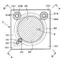
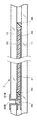
図1〜図5は本発明に係る液晶素子の一例を示したものであり、具体的には、光ディスク層において光ピックアップでの記録・再生時に生ずる収差を補正するための液晶収差補正素子に応用した例である。図1は液晶収差補正素子の平面図、図2は図1のA−A断面図、図3は図1のB−B断面図、図4は図1のS部分の拡大図、そして図5は液晶収差補正素子の電圧印加時の状態を説明した図である。
Hereinafter, the best mode for carrying out the present invention will be described.
FIGS. 1 to 5 show an example of the liquid crystal element according to the present invention. Specifically, the liquid crystal element is applied to a liquid crystal aberration correction element for correcting aberrations occurring during recording / reproduction with an optical pickup in an optical disk layer. This is an example. 1 is a plan view of the liquid crystal aberration correction element, FIG. 2 is a cross-sectional view taken along the line AA in FIG. 1, FIG. 3 is a cross-sectional view taken along the line BB in FIG. These are the figures explaining the state at the time of the voltage application of a liquid-crystal aberration correction element.
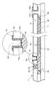
図1〜図3に示すように、液晶収差補正素子1は、セグメント電極20が形成された基板10と、コモン電極21が形成された基板11とで液晶40を挟みこむことにより概略構成されている。なお、図2及び図3では、セグメント電極20、コモン電極21と液晶40との間に一般的に設けられる液晶配向膜、透明絶縁層や、基板10、11上に設けられる反射防止膜等は図示を省略している。また、液晶40はシール材50によって内側に封入されている。また、電極20及び電極21には電圧を印加するためリード線等が接続されている。
As shown in FIGS. 1 to 3, the liquid crystal
そして、この実施形態では、図1及び図2に示すように、基板10に、液晶40と連通する孔60を形成し、その孔60に沿って鉢形の追従部材70を嵌め込んでいる。追従部材70は、孔60に対して接着し固定しても良いし、単に嵌め込んだ状態であっても良い。なお、追従部材70は基板10と基板11とを組み合わせる前に予め嵌め込んだ状態することが好ましい。さらに、追従部材70は別に作製し、それを後から基板10の孔60に嵌め込むこともできるし、あるいは、基板10の孔60に樹脂を流し込み、基板10上において直接に成形・硬化させることもできる。
In this embodiment, as shown in FIGS. 1 and 2, a
追従部材70は、好ましくはシリコーン樹脂、ポリオレフィン、ポリウレタン等の可撓性を有する樹脂材料から構成されている。厚みは、基板10の厚みとの関係で適宜設定されるが、液晶40の圧力で損傷されない程度であれば良く、具体的には50〜500μm程度である。
この追従部材70は、液晶40の膨張・収縮に応じて変形するようになっている。すなわち、環境の温度が上昇して液晶40が膨張し、内圧が大きくなった場合には、追従部材70の内底が持ち上がり、その変位した分に液晶40が流れ込む。また、反対に環境の温度が低下して液晶40が収縮した場合には、それに応じて追従部材70の内底が液晶40側へ変形することになる。したがって、液晶40自体の体積変化に応じて、液晶40が注入されている空間の容積が変化し、その結果、液晶層の厚みを常に一定に保つことができる。
The
The
また、この実施の形態では、図2に示すように、鉢形の追従部材の内底において周辺部70aを中心部70bよりも薄肉に形成している。これにより、液晶40の体積が変化したときに、内底の周辺部70aが他の部位に優先して容易に折れ曲がるので、内底全体が変形する場合に比べると、液晶40の膨張・収縮に対して円滑に追従することができ、変形量も大きくすることができる。
Further, in this embodiment, as shown in FIG. 2, the
なお、基板10、11としてはガラス基板等の透明基板が用いられる。また、セグメント電極20、コモン電極21としては、インジウム−スズ酸化膜を形成したITO等の透明電極が適宜採用される。
As the
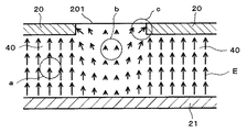
この実施の形態では、図4に示すように、セグメント電極20に対して、電極材の存在しない複数の非電極部位201が穴状に形成されている。そして、複数の非電極部位201は、セグメント電極20上の位置によって大きさ及び配置間隔を連続的に変化させている。なお、非電極部位201は、図1では便宜上少なく描いているが、実際には図4に示すように多数の非電極部位201が微細に形成されている。そして、この実施の形態(1)では、電極20上を同心円状に分けたときの半径方向Rに沿って、非電極部位201の大きさd1が大きい径から一旦小さい径となり再び大きい径となるように、また、配置間隔d2が広い間隔から一旦狭い間隔となり再び広い間隔となるように連続的なパターンを形成している。
In this embodiment, as shown in FIG. 4, a plurality of
セグメント電極20とコモン電極21との間に電圧を印加した場合、非電極部位201の近傍での電界Eの状態は図5に示すようになる。すなわち、セグメント電極20とコモン電極21とが対向している部分aでは、電極に垂直な方向へ強い電界が形成され、非電極部位201の中心部である部分bでは、やはり電極に垂直な方向へ弱い電界が形成される。そして、非電極部位201とセグメント電極20との境界に近い部分cでは、セグメント電極20へ向かって電界が傾いた状態となる。
When a voltage is applied between the
すると、液晶10の誘電異方性が正である場合には、液晶分子が電界Eに沿って配向するため、部分aでは液晶分子が電極に対して垂直に並び、部分bでは電界が弱いため電極に平行な状態のままとなり、部分cでは斜めに配向することになる。すなわち、非電極部位201の内側において液晶が不均一な配向状態となる。このとき、素子を通過する光(異常光)に対する屈折率は、非電極部位201の中心から周辺へ向かって連続的に小さくなる分布を形成するため、非電極部位201の部分においては凸レンズの効果を示すことになる。これにより、通過する光に位相差を与えることができる。
したがって、図4のように、非電極部位201の大きさ及び配置間隔を電極上の位置によって連続的に変化させた場合、それぞれの位置で得られる位相差は異なるため、発生する収差に応じて非電極部位201の配置パターンを適宜設計することで、素子全体として収差をリニアに補正することができる。
Then, when the dielectric anisotropy of the
Therefore, as shown in FIG. 4, when the size and arrangement interval of the
また、この実施の形態では、基板10の厚さ方向に穴30A、30Bが穿たれ、それらの穴にはセグメント電極20、コモン電極21へ接続するための端子31A、31Bがそれぞれ設けられている。基板11側に形成されたコモン電極21については、導通材80を介在させることにより基板10側の端子31Bと接続されている。なお、各端子は、穴の内周面に沿ってNi−Au等の金属をめっきする等して形成される。
図1のように各端子を基板10の面上に配置することにより、基板の側方に端子を集約配置する従来の素子に比べて、素子に偏った力が加わることなく、割れ・カケ等の不良が生じにくくなる。したがって、基板10、11をより薄く(例えば0.2mm)することが可能となり、素子を軽量化することができる。具体的には、従来に比して40%以上(従来の端子から面上配置の端子へ変更した効果が約10%、基板の厚さを0.3mmから0.2mmへ変更した効果が約33%)の軽量化となる。
In this embodiment, holes 30A and 30B are formed in the thickness direction of the
By arranging each terminal on the surface of the
また、この実施の形態では、基板10、11間に液晶40を注入するための注入口32が、基板10の面上に形成されている。注入口32の形状は円形、楕円形等であり、液晶40を注入した後に封止材90により適宜封止される。
特に、図1の例では、端子31A、31B、液晶の注入口32、及び追従部材70の全てが、対向する基板のうちの一方の基板10に配置されているため、生産する際に、個々の素子に切り分ける前の母材の状態で全ての端子等を形成でき、生産効率を向上させることができる。
In this embodiment, an
In particular, in the example of FIG. 1, the terminals 31 </ b> A and 31 </ b> B, the liquid
さらに、図1の例では、穴30A、30B、液晶の注入口32、及び追従部材70を、光束が通過する円形領域(セグメント電極20、コモン電極21が形成された領域)以外の、四角形状に形成された基板10上のコーナー部101付近に形成している。このようにすると、光束が通過しない基板10上の余剰部分を、端子等の位置として有効に利用することができるため、素子をより小型化することができる。また、端子等をコーナー部101に配置することにより、素子の重量バランスを最適化することができる。
Furthermore, in the example of FIG. 1, the holes 30 </ b> A and 30 </ b> B, the liquid
なお、上記実施の形態では、セグメント電極20に電極材の存在しない複数の非電極部位201を形成した場合について説明したが、同心円状に複数のセグメント電極を形成した場合であっても追従部材を同様に適用でき、この場合も、光の球面収差を良好に補正することができる。また、電極の配置パターンは同心円状に限られることなく、例えば、左右に分割した電極から構成することも可能である。この場合は、光ディスクの反り等によって発生するコマ収差を良好に補正することができる。
In the above-described embodiment, the case where a plurality of
また、対向する基板は、上記のように一対とは限らず、それ以上の基板が液晶を挟みつつ積層していても良い。 Further, the opposing substrates are not limited to a pair as described above, and more substrates may be stacked with the liquid crystal sandwiched therebetween.
そして、以上の実施形態では、端子等を基板10の表面に配置した例について説明したが、この他にも、例えば基板11を基板10よりも長く形成し、その長い部分に端子を集約配置した場合等にも上記の追従部材70を無論適用することができる。
And in the above embodiment, although the example which has arrange | positioned the terminal etc. on the surface of the board |
また、本発明の追従部材70は、図2のような鉢形のものに限られず、液晶40の膨張・収縮に応じて変形する形態であれば適宜採用することができる。例えば、基板10に形成した孔60の開口部を樹脂フィルムで覆う場合等を挙げることができる。この場合は、液晶40の体積変化に応じて樹脂フィルムが孔60の開口部より出っ張り、あるいは引き込まれることで液晶層の厚みが一定に保たれることとなる。
Further, the follow-
上述のような液晶収差補正素子1は、例えばレーザ光源、偏光子、1/2波長板、1/4波長板、対物レンズ、受光素子等とともに光ピックアップを構成し、光ディスク装置に組み込んで使用することができる。その際、温度が変化しても液晶層の厚みが一定であるため、高精度の収差補正が可能であり、次世代BD(Blu-ray Disc)や、多層ディスク等の高密度光ディスクにも好適に用いることができる。
The liquid crystal
なお、図1〜図5では、光ディスク装置において、光ピックアップでの記録・再生時に生ずる収差を補正するために用いる液晶収差補正素子の例について説明したが、その他にも、電極が形成された複数の基板で液晶を挟んだ構造からなる液晶素子であれば本発明の追従部材を同様に適用することができる。
具体的には、TFT、STN等の液晶表示素子や、液晶レンズ等が挙げられる。液晶表示素子の基板に孔を形成して追従部材を嵌め込む際には、追従部材が一箇所のみであると画面サイズが大きい場合に効果が小さくなる恐れがあるので、複数箇所に設けることができる。
1 to 5, examples of liquid crystal aberration correction elements used for correcting aberrations occurring during recording / reproduction with an optical pickup in the optical disc apparatus have been described. In addition, a plurality of electrodes on which electrodes are formed are also described. The follow-up member of the present invention can be similarly applied to any liquid crystal element having a structure in which the liquid crystal is sandwiched between the substrates.
Specifically, liquid crystal display elements such as TFT and STN, liquid crystal lenses, and the like can be given. When a hole is formed in the substrate of the liquid crystal display element and the follower member is fitted, if the follower member is only at one place, the effect may be reduced if the screen size is large. it can.
1 液晶収差補正素子
10、11 基板
101 コーナー部
20 セグメント電極
21 コモン電極
201 非電極部位
30A、30B、30C 穴
31A、31B、31C 端子
32 注入口
40 液晶
50 シール材
60 孔
70 追従部材
70a 周辺部
70b 中心部
80 導通材
90 封止材
E 電界
DESCRIPTION OF
Claims (4)
Priority Applications (1)
| Application Number | Priority Date | Filing Date | Title |
|---|---|---|---|
| JP2004105100A JP2005292326A (en) | 2004-03-31 | 2004-03-31 | Liquid crystal element |
Applications Claiming Priority (1)
| Application Number | Priority Date | Filing Date | Title |
|---|---|---|---|
| JP2004105100A JP2005292326A (en) | 2004-03-31 | 2004-03-31 | Liquid crystal element |
Publications (1)
| Publication Number | Publication Date |
|---|---|
| JP2005292326A true JP2005292326A (en) | 2005-10-20 |
Family
ID=35325344
Family Applications (1)
| Application Number | Title | Priority Date | Filing Date |
|---|---|---|---|
| JP2004105100A Pending JP2005292326A (en) | 2004-03-31 | 2004-03-31 | Liquid crystal element |
Country Status (1)
| Country | Link |
|---|---|
| JP (1) | JP2005292326A (en) |
Cited By (1)
| Publication number | Priority date | Publication date | Assignee | Title |
|---|---|---|---|---|
| JPWO2006035482A1 (en) * | 2004-09-27 | 2008-05-15 | 株式会社びにっと | Liquid crystal device having optical zoom function and method of manufacturing the same |
Citations (7)
| Publication number | Priority date | Publication date | Assignee | Title |
|---|---|---|---|---|
| JPH06337428A (en) * | 1993-05-28 | 1994-12-06 | Keibunshiya:Kk | Liquid crystal cell |
| JP2000047225A (en) * | 1998-07-31 | 2000-02-18 | Canon Inc | Liquid crystal display device |
| JP2000193953A (en) * | 1998-12-25 | 2000-07-14 | Ricoh Co Ltd | Liquid crystal element |
| JP2000227601A (en) * | 1998-11-30 | 2000-08-15 | Ricoh Co Ltd | Liquid crystal element |
| JP2002182181A (en) * | 2000-12-15 | 2002-06-26 | Olympus Optical Co Ltd | Liquid crystal lens |
| JP2002244101A (en) * | 2001-02-19 | 2002-08-28 | Sharp Corp | LCD display unit |
| JP2003045065A (en) * | 2001-07-30 | 2003-02-14 | Asahi Glass Co Ltd | Liquid crystal sealing element and optical head device |
-
2004
- 2004-03-31 JP JP2004105100A patent/JP2005292326A/en active Pending
Patent Citations (7)
| Publication number | Priority date | Publication date | Assignee | Title |
|---|---|---|---|---|
| JPH06337428A (en) * | 1993-05-28 | 1994-12-06 | Keibunshiya:Kk | Liquid crystal cell |
| JP2000047225A (en) * | 1998-07-31 | 2000-02-18 | Canon Inc | Liquid crystal display device |
| JP2000227601A (en) * | 1998-11-30 | 2000-08-15 | Ricoh Co Ltd | Liquid crystal element |
| JP2000193953A (en) * | 1998-12-25 | 2000-07-14 | Ricoh Co Ltd | Liquid crystal element |
| JP2002182181A (en) * | 2000-12-15 | 2002-06-26 | Olympus Optical Co Ltd | Liquid crystal lens |
| JP2002244101A (en) * | 2001-02-19 | 2002-08-28 | Sharp Corp | LCD display unit |
| JP2003045065A (en) * | 2001-07-30 | 2003-02-14 | Asahi Glass Co Ltd | Liquid crystal sealing element and optical head device |
Cited By (1)
| Publication number | Priority date | Publication date | Assignee | Title |
|---|---|---|---|---|
| JPWO2006035482A1 (en) * | 2004-09-27 | 2008-05-15 | 株式会社びにっと | Liquid crystal device having optical zoom function and method of manufacturing the same |
Similar Documents
| Publication | Publication Date | Title |
|---|---|---|
| US7710536B2 (en) | Liquid crystal diffraction lens element and optical head device | |
| EP1742099A1 (en) | Liquid crystal lens element and optical head | |
| JP4552556B2 (en) | Liquid crystal lens element and optical head device | |
| CN102804048B (en) | Multilayer structure liquid crystal optical element and manufacturing method thereof | |
| CN100409032C (en) | Double liquid crystal aberration correction element and manufacturing method thereof | |
| JP2005292326A (en) | Liquid crystal element | |
| KR100761951B1 (en) | Liquid crystal aberration correcting element, and production method therefore | |
| JP2011175104A (en) | Liquid crystal optical element having multilayer structure, and method for manufacturing liquid crystal lens | |
| CN101251657B (en) | Liquid crystal optical device and method for producing the same | |
| JP2009181142A (en) | Liquid crystal aberration correction element | |
| JP2011164427A (en) | Multilayered liquid crystal optical element and liquid crystal lens using the same | |
| CN100454412C (en) | Optical pickup device | |
| CN100394257C (en) | Liquid crystal aberration correction element | |
| JP2008176848A (en) | Liquid crystal element and optical head device | |
| JP4882737B2 (en) | Liquid crystal element and optical head device | |
| JP4379062B2 (en) | Optical device | |
| JP2003270656A (en) | Liquid crystal optical element | |
| JP4696883B2 (en) | Phase correction element and optical head device | |
| JP2002174804A (en) | Small-sized liquid crystal element | |
| JP2011150076A (en) | Liquid crystal optical element and method for manufacturing liquid crystal optical element | |
| JP2007248986A (en) | Liquid crystal aberration correction element and manufacturing method thereof | |
| JP2006058713A (en) | Liquid crystal optical element and optical head device | |
| JP4912997B2 (en) | Liquid crystal optical element and optical pickup device | |
| JP2006251431A (en) | Liquid crystal optical element and its manufacturing method | |
| JP2009186732A (en) | Liquid crystal optical element, method for manufacturing the same and optical head device |
Legal Events
| Date | Code | Title | Description |
|---|---|---|---|
| A621 | Written request for application examination |
Effective date: 20070228 Free format text: JAPANESE INTERMEDIATE CODE: A621 |
|
| A977 | Report on retrieval |
Free format text: JAPANESE INTERMEDIATE CODE: A971007 Effective date: 20091124 |
|
| A131 | Notification of reasons for refusal |
Effective date: 20091208 Free format text: JAPANESE INTERMEDIATE CODE: A131 |
|
| A02 | Decision of refusal |
Free format text: JAPANESE INTERMEDIATE CODE: A02 Effective date: 20100406 |